EP2800355B1 - Bildgebungsvorrichtung, verfahren zur steuerung der bildgebungsvorrichtung und steuerprogramm - Google Patents
Bildgebungsvorrichtung, verfahren zur steuerung der bildgebungsvorrichtung und steuerprogramm Download PDFInfo
- Publication number
- EP2800355B1 EP2800355B1 EP12863577.8A EP12863577A EP2800355B1 EP 2800355 B1 EP2800355 B1 EP 2800355B1 EP 12863577 A EP12863577 A EP 12863577A EP 2800355 B1 EP2800355 B1 EP 2800355B1
- Authority
- EP
- European Patent Office
- Prior art keywords
- pixels
- filter
- horizontal direction
- array
- vertical direction
- Prior art date
- Legal status (The legal status is an assumption and is not a legal conclusion. Google has not performed a legal analysis and makes no representation as to the accuracy of the status listed.)
- Not-in-force
Links
Images


Classifications
-
- H—ELECTRICITY
- H04—ELECTRIC COMMUNICATION TECHNIQUE
- H04N—PICTORIAL COMMUNICATION, e.g. TELEVISION
- H04N9/00—Details of colour television systems
- H04N9/01—Circuitry for demodulating colour component signals modulated spatially by colour striped filters by phase separation
-
- H—ELECTRICITY
- H04—ELECTRIC COMMUNICATION TECHNIQUE
- H04N—PICTORIAL COMMUNICATION, e.g. TELEVISION
- H04N25/00—Circuitry of solid-state image sensors [SSIS]; Control thereof
- H04N25/50—Control of the SSIS exposure
- H04N25/53—Control of the integration time
- H04N25/531—Control of the integration time by controlling rolling shutters in CMOS SSIS
-
- H—ELECTRICITY
- H04—ELECTRIC COMMUNICATION TECHNIQUE
- H04N—PICTORIAL COMMUNICATION, e.g. TELEVISION
- H04N23/00—Cameras or camera modules comprising electronic image sensors; Control thereof
- H04N23/80—Camera processing pipelines; Components thereof
- H04N23/84—Camera processing pipelines; Components thereof for processing colour signals
- H04N23/843—Demosaicing, e.g. interpolating colour pixel values
-
- H—ELECTRICITY
- H04—ELECTRIC COMMUNICATION TECHNIQUE
- H04N—PICTORIAL COMMUNICATION, e.g. TELEVISION
- H04N25/00—Circuitry of solid-state image sensors [SSIS]; Control thereof
- H04N25/10—Circuitry of solid-state image sensors [SSIS]; Control thereof for transforming different wavelengths into image signals
- H04N25/11—Arrangement of colour filter arrays [CFA]; Filter mosaics
- H04N25/13—Arrangement of colour filter arrays [CFA]; Filter mosaics characterised by the spectral characteristics of the filter elements
- H04N25/134—Arrangement of colour filter arrays [CFA]; Filter mosaics characterised by the spectral characteristics of the filter elements based on three different wavelength filter elements
-
- H—ELECTRICITY
- H04—ELECTRIC COMMUNICATION TECHNIQUE
- H04N—PICTORIAL COMMUNICATION, e.g. TELEVISION
- H04N25/00—Circuitry of solid-state image sensors [SSIS]; Control thereof
- H04N25/40—Extracting pixel data from image sensors by controlling scanning circuits, e.g. by modifying the number of pixels sampled or to be sampled
- H04N25/44—Extracting pixel data from image sensors by controlling scanning circuits, e.g. by modifying the number of pixels sampled or to be sampled by partially reading an SSIS array
- H04N25/447—Extracting pixel data from image sensors by controlling scanning circuits, e.g. by modifying the number of pixels sampled or to be sampled by partially reading an SSIS array by preserving the colour pattern with or without loss of information
-
- H—ELECTRICITY
- H04—ELECTRIC COMMUNICATION TECHNIQUE
- H04N—PICTORIAL COMMUNICATION, e.g. TELEVISION
- H04N25/00—Circuitry of solid-state image sensors [SSIS]; Control thereof
- H04N25/70—SSIS architectures; Circuits associated therewith
- H04N25/76—Addressed sensors, e.g. MOS or CMOS sensors
- H04N25/77—Pixel circuitry, e.g. memories, A/D converters, pixel amplifiers, shared circuits or shared components
- H04N25/778—Pixel circuitry, e.g. memories, A/D converters, pixel amplifiers, shared circuits or shared components comprising amplifiers shared between a plurality of pixels, i.e. at least one part of the amplifier must be on the sensor array itself
-
- H—ELECTRICITY
- H04—ELECTRIC COMMUNICATION TECHNIQUE
- H04N—PICTORIAL COMMUNICATION, e.g. TELEVISION
- H04N3/00—Scanning details of television systems; Combination thereof with generation of supply voltages
- H04N3/10—Scanning details of television systems; Combination thereof with generation of supply voltages by means not exclusively optical-mechanical
- H04N3/14—Scanning details of television systems; Combination thereof with generation of supply voltages by means not exclusively optical-mechanical by means of electrically scanned solid-state devices
- H04N3/15—Scanning details of television systems; Combination thereof with generation of supply voltages by means not exclusively optical-mechanical by means of electrically scanned solid-state devices for picture signal generation
- H04N3/1506—Scanning details of television systems; Combination thereof with generation of supply voltages by means not exclusively optical-mechanical by means of electrically scanned solid-state devices for picture signal generation with addressing of the image-sensor elements
- H04N3/1512—Scanning details of television systems; Combination thereof with generation of supply voltages by means not exclusively optical-mechanical by means of electrically scanned solid-state devices for picture signal generation with addressing of the image-sensor elements for MOS image-sensors, e.g. MOS-CCD
-
- H—ELECTRICITY
- H04—ELECTRIC COMMUNICATION TECHNIQUE
- H04N—PICTORIAL COMMUNICATION, e.g. TELEVISION
- H04N9/00—Details of colour television systems
- H04N9/03—Circuitry for demodulating colour component signals modulated spatially by colour striped filters by frequency separation
-
- H—ELECTRICITY
- H04—ELECTRIC COMMUNICATION TECHNIQUE
- H04N—PICTORIAL COMMUNICATION, e.g. TELEVISION
- H04N9/00—Details of colour television systems
- H04N9/64—Circuits for processing colour signals
- H04N9/648—Video amplifiers
-
- H—ELECTRICITY
- H04—ELECTRIC COMMUNICATION TECHNIQUE
- H04N—PICTORIAL COMMUNICATION, e.g. TELEVISION
- H04N2209/00—Details of colour television systems
- H04N2209/04—Picture signal generators
- H04N2209/041—Picture signal generators using solid-state devices
- H04N2209/042—Picture signal generators using solid-state devices having a single pick-up sensor
- H04N2209/045—Picture signal generators using solid-state devices having a single pick-up sensor using mosaic colour filter
Definitions
- the present invention relates to an imaging apparatus, and a control method and a control program for an imaging apparatus, and in particular to an imaging apparatus equipped with a color image pickup device, and a control method and control program for an imaging apparatus of the same.
- a primary color Bayer array (see, for example, Patent Documents 1 to 3), this being a color array widely employed in color image pickup devices, has red (R) and blue (B) placed in sequential lines of a chessboard pattern of green (G) pixels, green being the color to which the human eye is most sensitive and that contributes most to obtaining a brightness signal.
- the imaging device includes first green pixels and second green pixels adjacent to the respective first green pixels in a first direction, which is the direction, which is the direction in which electric charge accumulated in the pixels is read, wherein the dimension of the first and second green pixels in a second direction perpendicular to the first direction is twice the dimension of the first and second green pixels in the first direction.
- Patent Document 5 there is generally described a solid-state image pickup device, in which two rows and two columns are made a unit, describing a general thinning-out read method in relation to a modification of clock frequency.
- Patent Document 6 describes a solid-state image pickup device that enables vertical compression.
- Patent Document 7 describes color pixel arrays having common color filters for multiple adjacent pixels.
- Patent Document 8 describes a single sensor color camera with user selectable image record size.
- Patent Document 9 describes a low resolution verifier for a still video image.
- CMOS Complementary Metal Oxide Semiconductor
- a switch is provided to each photodiode, and, in cases in which charges are swept using a so-called “rolling shutter method", such as in video image capture, a shutter pulse is applied sequentially to each of every scan line, every plural pixels on each scan line, every single pixel, thereby performing sweeping of the charges accumulated in the photodiodes.
- reset is not performed all at once for all the pixels within a single screen, and reset, exposure start, and image capture signal reading is executed sequentially for each of every scan line, for every plural pixels on a scan line, or every single pixel on a scan line.
- reset, exposure, and reading are, for example, repeated for every scan line.
- the basic array pattern in order to obtain pixel signals for R, G, B, the minimum cycle for thinned reading in order to read lines configured from G pixels and R pixels, alternating with lines configured from G pixels and B pixels, is a vertical direction 1/3 thinning in which one line's worth of image data is read from every three lines. In such cases, plural line images are not read from within each common pixel, and the issues such as those described above do not arise.
- the basic array pattern is 3 ⁇ 3 or larger, it is normally preferable to match the size that is common for amplifiers etc. to the size of the basic array pattern for the following reason.
- a conceivable option is to pre-store the number (NK ⁇ KL) of correction coefficients, this corresponding to the lowest common multiple between the repetition cycle (N ⁇ M) of the basic array pattern and the repetition cycle (K ⁇ L) of the common amplifier structure, and then to select an appropriate correction coefficient for each pixel from these correction coefficients, and multiply the signal amount of each pixel by the selected correction coefficient.
- the color filter has a Bayer array of 2 ⁇ 2 and the amplifier sharing structure is also a four pixel square array of 2 ⁇ 2
- the number (NK ⁇ ML) of the correction coefficients becomes extremely large, increasing the correction processing time and the circuit scale. It is thereby preferable that the size of the common structure of the amplifier and the size of the basic array pattern match in order to lower the number of the correction coefficients.
- the color filter array is different from the Bayer array, thus it is sometimes possible to acquire pixel signals for R, G, and B even when reading the line image data using 1/2 thinning in the vertical direction.
- a hitherto normally preferred image pickup device in which the size of the common structure of the amplifier and the size of the basic array pattern match as described above, in cases in which the line image data is read by vertical direction 1/2 thinning in order to obtain the desired resolution, this results in plural line image data being read from within each common pixel, with the above issue arising of a large difference in exposure timing occurring.
- the present invention addresses the above issue, and an object thereof is to provide an imaging apparatus, and a control method and a control program for an imaging apparatus, that are capable of preventing a large difference from arising in exposure timing in cases in which plural pixels have a common amplifier, even when image data is read by thinning.
- an imaging apparatus of the present invention includes the features of claim 1.
- a control method for an imaging apparatus of the present invention includes the features of claim 5 .
- a control program of the present invention includes the features of claim 6.
- the advantageous effect is exhibited of enabling prevention of a large difference from arising in exposure timing in cases in which plural pixels have a common amplifier, even when image data is read by thinning.
- Fig. 1 is a schematic block diagram illustrating an imaging apparatus 10 according to the present exemplary embodiment.
- the imaging apparatus 10 is configured including an optical system 12, an image pickup device 14, an image capture processing section 16, an image processing section 20, a drive section 22, and a controller 24.
- the optical system 12 is configured including, for example, a lens set configured from plural optical lenses, an aperture adjustment mechanism, a zoom mechanism, and an automatic focusing mechanism.
- the image pickup device 14 is what is referred to as a 1-chip image pickup device configured by an image pickup device, for example a MOS type image sensor such as a Complementary Metal Oxide Semiconductor (CMOS), containing plural photoelectric conversion elements arrayed in the horizontal direction and vertical direction, with a color filter disposed above the image pickup device.
- CMOS Complementary Metal Oxide Semiconductor
- Fig. 2 illustrates a portion of a color filter according to the present exemplary embodiment.
- One out of 3 primary color filters, red (R), green (G) and blue (B), is placed over each of the pixels.
- the color filter of the first exemplary embodiment includes the following features (1) to (6).
- the color filter array has a repeatedly disposed basic array pattern of a predetermined pattern of (N ⁇ M) pixels (wherein N, M are integers of 3 or more) in the vertical direction and the horizontal direction of the 3 primary color filters red (R), green (G) and blue (B), wherein the green (G) filter, and at least one color filter out of the red (R) or the blue (B), are each placed in the vertical direction and the horizontal direction.
- the color filter is arrayed such that the respective filters of each color R, G, B (the R filters, G filters, B filters) have a specific periodicity.
- R filters, G filters and B filters with a specific periodicity enables processing to be performed in a repeating pattern during, for example, synchronization processing (also referred to as demosaic processing, the same applies below) of R, G, B signals read from the color image pickup device.
- synchronization processing also referred to as demosaic processing, the same applies below
- the color filter array illustrated in Fig. 2 has the G filter, that corresponds to the color contributing the most to obtaining a brightness signal (the color G in the present exemplary embodiment) placed in each line in the color filter array in the vertical direction that is the first direction, the horizontal direction that is the second direction, and third directions in the color filter plane that intersect with the first direction and the second direction, namely diagonal directions (NE, NW) (third directions).
- NE means a diagonal direction toward the top right
- NW means a diagonal direction toward the bottom right.
- the diagonal top right direction and the diagonal bottom right direction are each directions at 45° with respect to the horizontal direction.
- these are the directions of the pair of diagonals of a rectangle, and their angle varies according to the lengths of the long sides and the short sides.
- each of the R filter and the B filter is disposed in each line in the basic array pattern P in the vertical direction and horizontal direction of the color filter array.
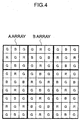
- Fig. 3 illustrates a state in which the basic array pattern P illustrated in Fig. 2 has been divided into 4 sets of 3 ⁇ 3 pixels.
- the basic array pattern P may be perceived as an A array of the 3 ⁇ 3 pixels surrounded by the solid line frame, and a B array of the 3 ⁇ 3 pixels surrounded by the broken line frame, arrayed so as to be alternately disposed along the horizontal and vertical directions.
- the G filters that are the brightness system pixels are placed at the 4 corners and at the center, thereby being placed over both diagonal lines.
- R filters are placed on both sides of the central G filter in the horizontal direction
- B filters are placed on both sides of the central G filter in the vertical direction
- R filters are placed on both sides of the central G filter in the vertical direction.
- the A array and the B array have reverse positional relationships for the R filters and the B filters, but have similar placement otherwise.
- the 4 corner G filters in the A array and the B array form square array G filters corresponding to 2 ⁇ 2 pixels.
- the color filter array (basic array pattern P) illustrated in Fig. 2 includes square arrays corresponding to 2 ⁇ 2 pixels configured by G filters.
- a 5 ⁇ 5 pixel local region centered on an A array is extracted from a mosaic image output from the image pickup device 14, the 2 ⁇ 2 pixels of G pixels at the 4 corners in the local region are disposed as illustrated in Fig. 5 .
- the vertical direction difference absolute value of the pixel values of these G pixels is (
- the difference absolute value in the horizontal direction is (
- the difference absolute value in the diagonal direction towards the top right is
- the difference absolute value in the diagonal direction towards the top left is
- the correlation (correlation direction) can then be determined as the direction with the smallest difference absolute value out of these four correlation absolute values.
- a 5 ⁇ 5 pixel local region is extracted from a mosaic image such that the 3 ⁇ 3 pixel A array is positioned at its center, there are 2 ⁇ 2 pixels of G pixels placed at the 4 corners thereof. Consequently, when the 3 ⁇ 3 pixels of the A array inside the above local region are pixels subject to synchronization processing, the sums (or the average values) of the correlation absolute values of the 4 corners are derived separately for each direction, and the direction having the smallest value out of the sums (or the average values) of the correlation absolute values for each direction is determined as the brightness correlation direction of the pixels subject to synchronization processing.
- the determined correlation direction may be employed when performing synchronization processing or the like.
- the basic array pattern P configuring the color filter array illustrated in Fig. 2 has point symmetry about the center of the basic array pattern (the center of the 4 G filters).
- each of the A array and the B array inside the basic array pattern also respectively have point symmetry about the central G filters, and also have top-bottom and left-right symmetry (line symmetry).
- This symmetry enables the circuit scale of a processing circuit at a later stage to be made smaller, and to be simplified.
- the size of the basic array pattern P that configures the color filter array illustrated in Fig. 2 is (N ⁇ M) pixels (wherein N, M are integers of 3 or more).
- the size of common pixels that are plural pixels that are common to a single amplifier is (K ⁇ L) pixels (wherein K. L are integers of 2 or more).
- the size of the basic array pattern P is greater than the size of the common pixels. Namely. N > K, and M > L is satisfied.
- the image pickup device 14 is, as described above, configured by a CMOS image sensor.
- Fig. 6 illustrates a schematic configuration of the image pickup device 14 configured by the CMOS image sensor.
- the image pickup device 14 is configured including a pixel array 30, a vertical drive scanning circuit 32, a column signal processing circuit 34. a horizontal drive scanning circuit 36, a signal line 38, and an amplifier 40, formed on a semiconductor substrate.
- the pixel array 30 includes plural pixels arrayed in a two dimensional pattern in the horizontal direction and the vertical direction.
- the vertical drive scanning circuit 32 selects and drives a collection of plural pixels on a scan line that runs along the horizontal direction. Note that it is also possible to select and drive pixels on a scan line one-by-one.
- the column signal processing circuit 34 is configured by plural signal processing circuits, not illustrated in the drawings. These signal processing circuits are provided one for each of the common pixels in the horizontal direction. Each of the signal processing circuits is configured including an analogue-to-digital converter (ADC) circuit, not illustrated in the drawings. These ADC circuits convert image capture signals into respective digital signals according to the pixel values of each of the pixels.
- ADC analogue-to-digital converter
- the horizontal drive scanning circuit 36 is configured by switches, not illustrated in the drawings, that are respectively connected to each of the plural signal processing circuits contained in the column signal processing circuit 34, and by a control circuit that performs ON/OFF control of the switches. By switching the switches ON, the image capture signals processed in the signal processing circuits are output to the signal line 38, and the image capture signals are output to the outside of the image pickup device 14 through the amplifier 40.
- the vertical drive scanning circuit 32, the column signal processing circuit 34, and the horizontal drive scanning circuit 36 are controlled by the drive section 22.
- K ⁇ L pixels (wherein K, L are integers of 2 or more) in the vertical direction and the horizontal direction configure common pixels, and the pixel array 30 is provided with an amplifier for each of the common pixels to amplify the image capture signals of each common pixel.
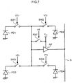
- Fig. 7 illustrates a configuration in which 2 ⁇ 2 pixels in the vertical direction and the horizontal direction, a total of 4 pixels, are configured as common pixels, and these 4 pixels are amplified by the same amplifier.
- cathodes of the photodiodes PD1 to PD4 that serve as pixels are each connected to one end of respective switches SW1 to SW4, each configured by, for example, a MOS transistor.
- the other ends of the switches SW1 to SW4 are connected to input terminals of a reset switch RST and an amplifier AP.
- the output terminal of the amplifier AP is connected to a signal line S.
- the signal line S is connected to the signal processing circuit of the column signal processing circuit 34, not illustrated in the drawings.
- the switches SW1 to SW4 are respectively input with charge transfer control signals VT1 to VT4 from the vertical drive scanning circuit 32.
- the vertical drive scanning circuit 32 switches ON the switches from which it is desired to read charges, such that charges accumulated on the photodiodes connected to the switches are amplified by the amplifier AP and output to the signal line S.
- configuration is made with one amplifier AP connected to each 2 ⁇ 2 pixels, as illustrated in Fig. 7 , thereby enabling a reduction in the number of switches, and enabling a higher degree of miniaturization.
- charge sweeping is performed by what is referred to as a rolling shutter method, in which charges accumulated in the photodiodes are swept by sequentially applying a shutter pulse to each of every scan line, every plural pixels on each scan line, or every single pixel.
- reset is not performed all at once for all the pixels within a single screen, and reset, exposure start, and image capture signal reading is executed sequentially for each of every scan line, every plural pixels on a scan line, or every single pixel.
- Fig. 9 For example, consider a case, such as illustrated in Fig. 9 , in which there are common pixels each of 3 ⁇ 3 pixels (illustrated by the bold lines in Fig. 9 ), and line image data is read at vertical direction 1/2 thinning, and horizontal direction 1/2 thinning.
- Fig. 9 taking positions in the vertical direction as rows, and positions in the horizontal direction as columns, each of the pixels within each common pixel is numbered respectively as a pixel 1 to 9, and pixel data is read for each pixel in every second row for vertical direction 1/2 thinning.
- pixel data is read for each pixel in every second column for horizontal direction 1/2 thinning. Pixel values are accordingly read for the pixels that are shaded in Fig. 9 .
- the pixel 1 in the first row and the first column, the pixel 3 in the first row and third column, the pixel 7 in the third row and the first column, and the pixel 9 in the third row and the third column are pixels within a common pixel of 3 ⁇ 3 pixels. Since a single amplifier is common to each common pixel, it is not possible to read the pixel data of these 4 individual pixels all at once.
- a first scan scanning, that is to say reset (R), exposure (1_exposure) and reading (acquisition), is performed for the pixels 1 that, out of the respective pixels 1 in the first row, are positioned to be read in horizontal direction 1/2 thinning, so as to scan the pixel 1 in the first row and the first column, the pixel 1 in the first row and the seventh column, the pixel 1 in the first row and the thirteenth column, and so on.
- the next scan is started. Namely, reset (R), exposure (2_exposure) and reading (acquisition) are performed for the pixels 2 that, out of the respective pixels 2 in the first row, are positioned to be read in horizontal direction 1/2 thinning, so as to scan the pixel 2 in the first row and the fifth column, the pixel 2 in the first row and the eleventh column, the pixel 2 in the first row and the seventeenth column, and so on.
- reset (R), exposure (3_exposure) and reading (acquisition) are performed for the pixels 3 that, out of the respective pixels 3 in the first row, are positioned to be read in horizontal direction 1/2 thinning, so as to scan the pixel 3 in the first row and the third column, the pixel 3 in the first row and the ninth column, the pixel 3 in the first row and the fifteenth column, and so on.
- scanning is performed 3 times each for the third row and the fifth row, similarly to for the first row. Accordingly, for common pixels of 3 ⁇ 3 pixels, when reading of pixels data of for each pixel is performed by 1/2 thinning in the vertical direction and the horizontal direction, scanning needs to be performed 3 times for each row, since the plural pixels in both the vertical direction and the horizontal direction within each of the common pixels need to be read. Since there are different exposure timings even for pixels within the same row, when, for example, attempting to capture a video image of a fast moving subject the precision of interpolation processing, such as synchronization processing, deteriorates due to variation in signal amount within pixel units, sometimes giving rise to false color.
- the placement of pixels after thinning is the placement illustrated in Fig. 11 .
- the pixels 1, 3, 5, 7, 9 at the 4 corners within the same common pixel are each G pixels, and each has a different respective exposure timing. Therefore, since in particular the pixels 1, 3, 7, 9 indicated in the broken line regions are placed as 2 ⁇ 2 pixels adjacent to one another, this exacerbates the undesirable effects caused by steps in signal amounts due to different exposure timings.
- the image pickup device 14 is driven so as to read line image data of lines running along the horizontal direction at a cycle of K pixels or greater in the vertical direction.
- line image data running along the horizontal direction is read at a cycle of 2 line cycles or greater in the vertical direction. Accordingly, there is not plural line image data running along the horizontal direction read from within each of the common pixels in the vertical direction, enabling large differences in exposure timing to be prevented from occurring.
- pixel data is not read from plural pixels within each of the common pixels in the horizontal direction, enabling large differences in exposure timing to be prevented.
- the image capture processing section 16 performs predetermined processing such as amplification processing, correlation double sampling processing, or A/D conversion processing on image capture signals output from the image pickup device 14, and then outputs as image data to the image processing section 20.
- predetermined processing such as amplification processing, correlation double sampling processing, or A/D conversion processing
- the image processing section 20 subjects the image data output from the image capture processing section 16 to what is referred to as synchronization processing. Namely, for all the pixels, interpolation is performed of image data for colors other than the corresponding respective color from pixel data of peripheral pixels, so as to generate R, G, B image data for all pixels. Then, what is referred to as YC conversion processing is performed to the generated R, G, B image data, to generate brightness data Y and color difference data Cr, Cb. Resizing processing is then performed to re-size these signals to a size according to the image capture mode.
- the drive section 22 performs for example driving to read image capture signals from the image pickup device 14 according to instruction from the controller 24.
- the controller 24 performs overall control of the drive section 22, the image processing section 20 and so on according to such factors as the image capture mode. Although discussed in detail later, put briefly, the controller 24 instructs the drive section 22 to read image capture signals with a reading method corresponding to the image capture mode, and instructs the image processing section 20 to perform image processing corresponding to the image capture mode.
- the controller 24 instructs the drive section 22 so as to thin with a thinning method according to the instructed image capture mode and to read the image capture signals.
- image capture modes include a still image mode in which a still image is captured, and video modes including an HD video mode that thins a captured image and generates High Definition (HD) video data at a comparatively high resolution and records this on a recording medium such as a memory card, not illustrated in the drawings, and a through video mode (live view mode) in which a captured image is thinned and a through video (live view image) of comparatively low resolution is output to a display section, not illustrated in the drawings, however there is no limitation of the types of image capture modes thereto.
- HD High Definition
- the processing illustrated in Fig. 12 is executed when instruction has been given to execute imaging according to an image capture mode.
- the following explanation describes a case in which line image data is read at a predetermined cycle in the vertical direction, namely a case in which reading is performed in which lines other than lines of the predetermined cycle in the vertical direction are thinned (left out).
- the line image data in this case is a collection of pixel data of pixels in a row running along the horizontal direction.
- the drive section 22 is instructed to read image data using a thinning method corresponding to the image capture mode.
- the image pickup device 14 is driven so as to read line image data from lines running along the horizontal direction at a cycle of 2 lines or greater in the vertical direction, and also only pixels that are at a cycle of 2 pixels or greater in the horizontal direction are read out of all of the pixels in the lines running along the horizontal direction.
- the controller 24 instructs the drive section 22 to read at 1/2 thinning in both the vertical direction and the horizontal direction (in the present exemplary embodiment, the drive section 22 and the controller 24 correspond to line image data generation means).
- pixel data is read from the pixels that are shaded in Fig. 13 . Namely, pixel data is read at a 2 pixel cycle in the vertical direction and the horizontal direction.
- each of the pixels within each common pixel of 2 ⁇ 2 pixels is numbered respectively as a pixel 1 to 4, and in the first scan, scanning is performed for all of the pixels 1 in the first row are read, so as to scan the pixel 1 in the first row and the first column, the pixel 1 in the first row and the third column, the pixel 1 in the first row and the fifth column, and so on.
- reset (R), exposure (1_exposure), and reading (acquisition) are performed for all of the pixels 1 in the first row.
- the next scan is started. Namely, reset (R), exposure (2_exposure), and reading (acquisition) are performed for all of the pixels 1 in the third row, so as to scan the pixel 1 in the third row and the first column, the pixel 1 in the third row and the third column, the pixel 1 in the third row and the fifth column, and so on.
- the next scan is started. Namely, reset (R), exposure (3_exposure), and reading (acquisition) are performed for all of the pixels 1 in the fifth row, so as to scan the pixel 1 in the fifth row and the first column, the pixel 1 in the fifth row and the third column, the pixel 1 in the fifth row and the fifth column, and so on.
- scanning is performed 1 time each for the fifth row, the seventh row, the ninth row and so on, similarly to for the first row. Accordingly, for each common pixel of 2 ⁇ 2 pixels, 1 time of scanning per row is sufficient due to reading at a cycle of both the vertical direction number and the horizontal direction number of pixels in each of the common pixels or greater, even when reading pixel data of each of the pixels using 1/2 thinning in both the vertical direction and the horizontal direction.
- the image processing section 20 is instructed to execute image processing (such as synchronization processing, YC conversion processing, resizing processing) on the thinned and read image data according to the image capture mode (in the present exemplary embodiment, the image processing section 20 and the controller 24 correspond to image data generation means).
- image processing such as synchronization processing, YC conversion processing, resizing processing
- controller 24 and the image processing section 20 may be configured with a computer that includes for example a CPU, ROM, RAM and non-volatile ROM.
- a processing program for the above processing may, for example, be pre-stored on the non-volatile ROM, and then executed by reading into the CPU.
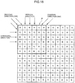
- Fig. 18 illustrates a color filter according to the present exemplary embodiment.
- the color filter according to the present exemplary embodiment includes a basic array pattern P (the pattern indicated by the bold frame) formed from a square array pattern corresponding to 6 ⁇ 6 pixels, with the basic array pattern P disposed so as to repeat in both the horizontal direction and the vertical direction.
- the color filter is arrayed such that the respective filters of each color R. G, B (the R filters. G filters. B filters) have a specific periodicity.
- the G filter is placed in each line of the color filter array in both the vertical direction and horizontal direction.
- one or more respectively of the R filter and the B filter is placed in the basic array pattern P in each of the lines of the color filter array in both the vertical direction and horizontal direction.
- Fig. 19 illustrates a state in which the basic array pattern P illustrated in Fig. 18 has been divided into 4 sets of 3 ⁇ 3 pixels.
- the basic array pattern P illustrated in Fig. 19 may be perceived an A array of the 3 ⁇ 3 pixels surrounded by the solid line frame, and a B array of the 3 ⁇ 3 pixels surrounded by the broken line frame, arrayed so as to be alternately disposed along the horizontal and vertical directions.
- the R filter is placed at the center, and the B filters are placed at the 4 corners, and G filters are placed on both sides of the central R filter at the top and bottom, and left and right.
- the B filter is placed at the center, and the R filters are placed at the 4 corners, and G filters are placed on both sides of the central B filter at the top and bottom, and left and right.
- the A array and the B array have reverse positional relationships for the R filters and the B filters, but have similar placement otherwise.
- the color filter of the second exemplary embodiment may be perceived as the A array and the B array, alternately disposed in the vertical direction and the horizontal direction.
- a 5 ⁇ 5 pixel local region (a region illustrated by a bold line frame) centered on an A array is extracted from a mosaic image output from the image pickup device 14.
- the 8 individual G pixels within this local region are placed in a cross shape, as illustrated in Fig. 20B .
- the G pixels therein are denoted, in sequence from left to right, G1, G2, G3. G4. and in sequence from top to bottom, G5.
- the pixels G1, G2, and the pixels G2, G3 are in adjacent contact with each other in the horizontal direction
- the pixels G3, G4 and the pixels G7, G8 are in adjacent contact with each other in the vertical direction
- the pixels G6, G3 and the pixels G2, G7 are in adjacent contact with each other in the diagonal direction toward the top left
- the pixels G6, G2 and the pixels G3, G7 are in adjacent contact with each other in the diagonal direction toward the top right.
- the sum of the difference absolute values in the horizontal direction is
- the sum of the difference absolute values in the vertical direction is
- the sum of the difference absolute values in the diagonal direction towards the top right is
- the sum of the difference absolute values in the diagonal direction towards the top left is
- the correlation can then be determined as the direction with the smallest difference absolute value out of these four correlation absolute values. Note that the determined correlation direction can be employed during the performance of processing such as synchronization processing.
- the basic array pattern P that configures the color filter illustrated in Fig. 18 has point symmetry about the center of the basic array pattern P.
- the A array and the B array within the basic array pattern each have point symmetry about a central R filter, or B filter, and are top-bottom and left-right symmetrical (have line symmetry).
- the size of the basic array pattern P that configures the color filter array illustrated in Fig. 18 is (N ⁇ M) pixels (wherein N, M are integers of 3 or more), which is greater than the common pixel size of (K ⁇ L) pixels (wherein K, L are integers of 2 or more). Namely. N > K, and M > L is satisfied.
- the color filter according to the second exemplary embodiment accordingly has the same features to the features (1), and (3) to (6) of the color filter according to the first exemplary embodiment.
- Features (2), (3) incorporate the feature that 1 or more of each of the G filter, the R filter, and the B filter is placed in each of the lines in the vertical direction and horizontal direction of the color filter array within the basic array pattern P.
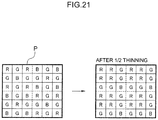
- the image after thinning is the image as illustrated in Fig. 21 .
- color filter array is not limited to those described in each of the exemplary embodiments, and the present invention may also be applied to an imaging apparatus having an image pickup device with the following color filter array.
- a color filter array having the above features (1), (2), (3) and (6) there is, for example, a color filter in which the basic array pattern P is a 3 ⁇ 3 pixel color filter as illustrated in Fig. 22 .
- This color filter array is configured by a repeating basic pattern with the G filters placed at the center and the 4 corners out of the 3 ⁇ 3 pixels, and the same number each of R and B placed on the remaining 4 pixels.
- An image from 1/2 thinning in both the vertical direction and horizontal direction is an image such as the one illustrated in Fig. 22 .
- pixel signals in all pixels' worth of pixels may be read and temporarily stored, in memory such as RAM, and then image data generated by selectively using the pixel data of pixels that are at 2 pixel cycles in the vertical direction and the horizontal direction (in this embodiment, the image capture processing section 16 or the image processing section 20 corresponds to the line image data generation means).
Landscapes
- Engineering & Computer Science (AREA)
- Multimedia (AREA)
- Signal Processing (AREA)
- Physics & Mathematics (AREA)
- Spectroscopy & Molecular Physics (AREA)
- Color Television Image Signal Generators (AREA)
- Optical Filters (AREA)
- Transforming Light Signals Into Electric Signals (AREA)
Claims (6)
- Bildgebungsvorrichtung, umfassend:eine Bildaufnahmevorrichtung (14), die eine Vielzahl von fotoelektrischen Umwandlungselementen, die in einer vertikalen Richtung und in einer horizontalen Richtung angeordnet sind, umfasst;ein Verstärkungsmittel (AP), das einen Verstärker (AP) für jedes der gemeinsamen Pixel umfasst, wobei jedes gemeinsame Pixel K x L Pixel, also K Pixel in vertikaler Richtung und L Pixel in horizontaler Richtung, aufweist, wobei K, L ganze Zahlen im Wert von 2 oder mehr sind, und ein Bilderfassungssignal für jedes der gemeinsamen Pixel verstärkt;einen Farbfilter, der oberhalb einer Vielzahl von Pixeln vorgesehen ist, die durch die Vielzahl von fotoelektrischen Umwandlungselementen konfiguriert sind,wobei der Farbfilter eine wiederholt angeordnete Grundanordnungsstruktur (P) besitzt, die einen ersten Filter, der einer ersten Farbe entspricht, die am meisten zum Erhalten eines Helligkeitssignals beiträgt, und zweite Filter, die jeweils 2 oder mehr zweiten Farben entsprechen, die nicht die erste Farbe sind, aufweist, die in einer vorbestimmten Struktur von N x M Pixeln, also N Pixeln in der vertikalen Richtung und M Pixeln in der horizontalen Richtung, platziert sind, wobei N > K und M > L ist,wobei die Grundanordnungsstruktur (P) so angeordnet ist, dass sie sich in einer vertikalen Richtung wiederholt und dass sie sich in einer horizontalen Richtung wiederholt,ein Linienbilddatenerzeugungsmittel, das Linienbilddaten erzeugt, indem esLadungsdurchsuchung unter Verwendung eines Rollladenverfahrens durchführt, bei dem in den fotoelektrischen Umwandlungselementen angesammelte Ladungen durch aufeinanderfolgendes Anlegen von Rollladenimpulsen an die Bildaufnahmevorrichtung (14) nacheinander an jedes Pixel oder an jede Abtastlinie, die in der horizontalen Richtung verläuft, oder an jede Vielzahl von Pixeln auf einer Abtastlinie, die in der horizontalen Richtung verläuft, durchsucht werden,Linienbilddaten von Linien, die in der horizontalen Richtung in einem Zyklus von K Pixeln in der vertikalen Richtung verlaufen, liest und Pixel auf den gelesenen Linien, die in der horizontalen Richtung in einem Zyklus von L Pixeln verlaufen, ausliest,ein Bilddatenerzeugungsmittel (20), das Bilddaten basierend auf den Linienbilddaten erzeugt;wobeider Farbfilter einen R-Filter, einen G-Filter und einen B-Filter aufweist, die den Farben Rot (R), Grün (G) bzw. Blau (B) entsprechen; unddadurch gekennzeichnet, dassder Farbfilter durch eine erste Anordnung und eine zweite Anordnung konfiguriert ist, die abwechselnd in der vertikalen Richtung und der horizontalen Richtung angeordnet sind, wobei die vertikale Anordnung 3 x 3 Pixeln entspricht, wobei der G-Filter in der Mitte und an den 4 Ecken platziert ist, der B-Filter oberhalb und unterhalb des zentralen G-Filters platziert ist und der R-Filter links und rechts von dem zentralen G-Filter platziert ist, und die zweite Anordnung 3 x 3 Pixeln entspricht, wobei der G-Filter in der Mitte und an den 4 Ecken platziert ist, der R-Filter oberhalb und unterhalb des zentralen G-Filters platziert ist und der B-Filter links und rechts von dem zentralen G-Filter platziert ist; oderder Farbfilter durch eine erste Anordnung und eine zweite Anordnung konfiguriert ist, die abwechselnd in der vertikalen Richtung und der horizontalen Richtung angeordnet sind, wobei die erste Anordnung 3 x 3 Pixeln entspricht, wobei der R-Filter in der Mitte platziert ist, der B-Filter an den 4 Ecken platziert ist und der G-Filter oberhalb und unterhalb des zentralen R-Filters sowie links und rechts davon platziert ist, und die zweite Anordnung 3 x 3 Pixeln entspricht, wobei der B-Filter in der Mitte platziert ist, der R-Filter an den 4 Ecken platziert ist und der G-Filter oberhalb und unterhalb des zentralen B-Filters sowie links und rechts davon platziert ist.
- Bildgebungsvorrichtung nach Anspruch 1, wobei:einer oder mehrere des ersten Filters in jeder Linie in dem Farbfilter in der vertikalen Richtung, der horizontalen Richtung und weiteren Richtungen platziert ist, die sich mit der vertikalen Richtung und der horizontalen Richtung schneiden; unddie zweiten Filter, die jeweils jeder Farbe der zweiten Farben entsprechen, so platziert sind, dass 1 oder mehrere von jedem in jeder Linie in der Grundanordnungsstruktur in der vertikalen Richtung und in der horizontalen Richtung vorkommen.
- Bildgebungsvorrichtung nach Anspruch 1 oder 2, wobei:der Farbfilter eine quadratische Anordnung, die 2 × 2 Pixeln entspricht, aufweist, die aus dem ersten Filter konfiguriert ist.
- Bildgebungsvorrichtung nach einem der Ansprüche 1 bis 3, wobei:die erste Farbe Grün (G) ist und die zweiten Farben Rot (R) und Blau (B) sind.
- Steuerverfahren für eine Bildgebungsvorrichtung, die eine Bildaufnahmevorrichtung (14) umfasst, wobei die Bildaufnahmevorrichtung umfasst: eine Vielzahl von fotoelektrischen Umwandlungselementen, die in einer vertikalen Richtung und in einer horizontalen Richtung angeordnet sind, ein Verstärkungsmittel (AP), das einen Verstärker (AP) für jedes der gemeinsamen Pixel umfasst, wobei jedes gemeinsame Pixel K x L Pixel, also K Pixel in der vertikalen Richtung und L Pixel in der horizontalen Richtung, aufweist, wobei K, L ganze Zahlen im Wert von 2 oder mehr sind, und ein Bilderfassungssignal für jedes der gemeinsamen Pixel verstärkt, einen Farbfilter, der oberhalb einer Vielzahl von Pixeln vorgesehen ist, die durch die Vielzahl von fotoelektrischen Umwandlungselementen konfiguriert sind, wobei der Farbfilter eine wiederholt angeordnete Grundanordnungsstruktur (P) besitzt, die einen ersten Filter, der einer ersten Farbe entspricht, die am meisten zum Erhalten eines Helligkeitssignals beiträgt, und zweite Filter, die jeweils 2 oder mehr zweiten Farben entsprechen, die nicht die erste Farbe sind, aufweist, die in einer vorbestimmten Struktur von N x M Pixeln, also N Pixeln in der vertikalen Richtung und M Pixeln in der horizontalen Richtung, platziert sind, wobei N > K und M > L ist, wobei die Grundanordnungsstruktur (P) so angeordnet ist, dass sie sich in einer vertikalen Richtung wiederholt und dass sie sich in einer horizontalen Richtung wiederholt,
der Farbfilter einen R-Filter, einen G-Filter und einen B-Filter aufweist, die den Farben Rot (R), Grün (G) bzw. Blau (B) entsprechen; und
der Farbfilter durch eine erste Anordnung und eine zweite Anordnung konfiguriert ist, die abwechselnd in der vertikalen Richtung und der horizontalen Richtung angeordnet sind, wobei die vertikale Anordnung 3 x 3 Pixeln entspricht, wobei der G-Filter in der Mitte und an den 4 Ecken platziert ist, der B-Filter oberhalb und unterhalb des zentralen G-Filters platziert ist und der R-Filter links und rechts von dem zentralen G-Filter platziert ist, und die zweite Anordnung 3 x 3 Pixeln entspricht, wobei der G-Filter in der Mitte und an den 4 Ecken platziert ist, der R-Filter oberhalb und unterhalb des zentralen G-Filters platziert ist und der B-Filter links und rechts von dem zentralen G-Filter platziert ist; oder
der Farbfilter durch eine erste Anordnung und eine zweite Anordnung konfiguriert ist, die abwechselnd in der vertikalen Richtung und der horizontalen Richtung angeordnet sind, wobei die erste Anordnung 3 x 3 Pixeln entspricht, wobei der R-Filter in der Mitte platziert ist, der B-Filter an den 4 Ecken platziert ist und der G-Filter oberhalb und unterhalb des zentralen R-Filters sowie links und rechts davon platziert ist, und die zweite Anordnung 3 x 3 Pixeln entspricht, wobei der B-Filter in der Mitte platziert ist, der R-Filter an den 4 Ecken platziert ist und der G-Filter oberhalb und unterhalb des zentralen B-Filters sowie links und rechts davon platziert ist;
wobei das Steuerverfahren umfasst:Erzeugen von Linienbilddaten durchDurchführen von Ladungsdurchsuchung unter Verwendung eines Rollladenverfahrens, bei dem in den fotoelektrischen Umwandlungselementen angesammelte Ladungen durch aufeinanderfolgendes Anlegen von Rollladenimpulsen an die Bildaufnahmevorrichtung (14) nacheinander an jedes Pixel oder an jede Abtastlinie, die in der horizontalen Richtung verläuft, oder an jede Vielzahl von Pixeln auf einer Abtastlinie, die in der horizontalen Richtung verläuft, durchsucht werden,Lesen von Linienbilddaten von Linien, die in der horizontalen Richtung in einem Zyklus von K Pixeln in der vertikalen Richtung verlaufen, undAuslesen von Pixeln auf den gelesenen Linien, die in der horizontalen Richtung in einem Zyklus von L Pixeln verlaufen, undErzeugen von Bilddaten basierend auf den Linienbilddaten. - Steuerprogramm, das das Ausführen von Verarbeitung in einem Computer verursacht, der eine mit einer Bildaufnahmevorrichtung (14) ausgestattete Bildgebungsvorrichtung steuert, wobei
die Bildaufnahmevorrichtung (14) umfasst: eine Vielzahl von fotoelektrischen Umwandlungselementen, die in einer vertikalen Richtung und in einer horizontalen Richtung angeordnet sind, ein Verstärkungsmittel (AP) für jedes der gemeinsamen Pixel, wobei jedes gemeinsame Pixel K x L Pixel, also K Pixel in der vertikalen Richtung und L Pixel in der horizontalen Richtung, aufweist, wobei K, L ganze Zahlen im Wert von 2 oder mehr sind, und das ein Bilderfassungssignal für jedes der gemeinsamen Pixel verstärkt, einen Farbfilter, der oberhalb einer Vielzahl von Pixeln vorgesehen ist, die durch die Vielzahl von fotoelektrischen Umwandlungselementen konfiguriert sind, wobei der Farbfilter eine wiederholt angeordnete Grundanordnungsstruktur (P) besitzt, die einen ersten Filter, der einer ersten Farbe entspricht, die am meisten zum Erhalten eines Helligkeitssignals beiträgt, und zweite Filter, die jeweils 2 oder mehr zweiten Farben entsprechen, die nicht die erste Farbe sind, aufweist, die in einer vorbestimmten Struktur von N x M Pixeln, also N Pixeln in der vertikalen Richtung und M Pixeln in der horizontalen Richtung, platziert sind, wobei N > K und M > L ist, wobei die Grundanordnungsstruktur (P) so angeordnet ist, dass sie sich in einer vertikalen Richtung wiederholt und dass sie sich in einer horizontalen Richtung wiederholt, und
der Farbfilter durch eine erste Anordnung und eine zweite Anordnung konfiguriert ist, die abwechselnd in der vertikalen Richtung und der horizontalen Richtung angeordnet sind, wobei die vertikale Anordnung 3 x 3 Pixeln entspricht, wobei der G-Filter in der Mitte und an den 4 Ecken platziert ist, der B-Filter oberhalb und unterhalb des zentralen G-Filters platziert ist und der R-Filter links und rechts von dem zentralen G-Filter platziert ist, und die zweite Anordnung 3 x 3 Pixeln entspricht, wobei der G-Filter in der Mitte und an den 4 Ecken platziert ist, der R-Filter oberhalb und unterhalb des zentralen G-Filters platziert ist und der B-Filter links und rechts von dem zentralen G-Filter platziert ist; oder
der Farbfilter durch eine erste Anordnung und eine zweite Anordnung konfiguriert ist, die abwechselnd in der vertikalen Richtung und der horizontalen Richtung angeordnet sind, wobei die erste Anordnung 3 x 3 Pixeln entspricht, wobei der R-Filter in der Mitte platziert ist, der B-Filter an den 4 Ecken platziert ist und der G-Filter oberhalb und unterhalb des zentralen R-Filters sowie links und rechts davon platziert ist, und die zweite Anordnung 3 x 3 Pixeln entspricht, wobei der B-Filter in der Mitte platziert ist, der R-Filter an den 4 Ecken platziert ist und der G-Filter oberhalb und unterhalb des zentralen B-Filters sowie links und rechts davon platziert ist;
wobei die Verarbeitung umfasst:Erzeugen von Linienbilddaten durchDurchführen von Ladungsdurchsuchung unter Verwendung eines Rollladenverfahrens, bei dem in den fotoelektrischen Umwandlungselementen angesammelte Ladungen durch aufeinanderfolgendes Anlegen von Rollladenimpulsen an die Bildaufnahmevorrichtung (14) nacheinander an jedes Pixel oder an jede Abtastlinie, die in der horizontalen Richtung verläuft, oder an jede Vielzahl von Pixeln auf einer Abtastlinie, die in der horizontalen Richtung verläuft, durchsucht werden,Lesen von Linienbilddaten von Linien, die in der horizontalen Richtung in einem Zyklus von K Pixeln in der vertikalen Richtung verlaufen, undAuslesen von Pixeln auf den gelesenen Linien, die in der horizontalen Richtung in einem Zyklus von L Pixeln verlaufen, undErzeugen von Bilddaten basierend auf den Linienbilddaten.
Applications Claiming Priority (2)
| Application Number | Priority Date | Filing Date | Title |
|---|---|---|---|
| JP2011286688 | 2011-12-27 | ||
| PCT/JP2012/083973 WO2013100093A1 (ja) | 2011-12-27 | 2012-12-27 | 撮像装置、撮像装置の制御方法、及び制御プログラム |
Publications (3)
| Publication Number | Publication Date |
|---|---|
| EP2800355A1 EP2800355A1 (de) | 2014-11-05 |
| EP2800355A4 EP2800355A4 (de) | 2015-08-12 |
| EP2800355B1 true EP2800355B1 (de) | 2017-12-20 |
Family
ID=48697572
Family Applications (1)
| Application Number | Title | Priority Date | Filing Date |
|---|---|---|---|
| EP12863577.8A Not-in-force EP2800355B1 (de) | 2011-12-27 | 2012-12-27 | Bildgebungsvorrichtung, verfahren zur steuerung der bildgebungsvorrichtung und steuerprogramm |
Country Status (5)
| Country | Link |
|---|---|
| US (1) | US8964087B2 (de) |
| EP (1) | EP2800355B1 (de) |
| JP (1) | JP5607265B2 (de) |
| CN (1) | CN104025566B (de) |
| WO (1) | WO2013100093A1 (de) |
Families Citing this family (4)
| Publication number | Priority date | Publication date | Assignee | Title |
|---|---|---|---|---|
| CN104429061B (zh) * | 2012-07-06 | 2016-04-13 | 富士胶片株式会社 | 彩色摄像元件和摄像装置 |
| JP2015201724A (ja) * | 2014-04-07 | 2015-11-12 | キヤノン株式会社 | 画像処理装置および画像処理方法 |
| US10151862B2 (en) | 2016-04-27 | 2018-12-11 | Visera Technologies Company Limited | Color filter array having low density of blue color |
| CN116863869B (zh) * | 2023-09-04 | 2023-12-12 | 长春希达电子技术有限公司 | 一种亚像素的排布结构及其控制方法 |
Family Cites Families (28)
| Publication number | Priority date | Publication date | Assignee | Title |
|---|---|---|---|---|
| US4876590A (en) * | 1988-06-17 | 1989-10-24 | Eastman Kodak Company | Low resolution verifier for a still video image |
| US5493335A (en) * | 1993-06-30 | 1996-02-20 | Eastman Kodak Company | Single sensor color camera with user selectable image record size |
| JPH0823543A (ja) | 1994-07-07 | 1996-01-23 | Canon Inc | 撮像装置 |
| JPH0823542A (ja) | 1994-07-11 | 1996-01-23 | Canon Inc | 撮像装置 |
| EP0930789B1 (de) | 1998-01-20 | 2005-03-23 | Hewlett-Packard Company, A Delaware Corporation | Farbbildaufnahmegerät |
| JP4098438B2 (ja) | 1999-04-15 | 2008-06-11 | オリンパス株式会社 | カラー撮像素子及びカラー撮像装置 |
| JP4487351B2 (ja) * | 1999-07-15 | 2010-06-23 | ソニー株式会社 | 固体撮像素子およびその駆動方法並びにカメラシステム |
| JP4518616B2 (ja) * | 2000-04-13 | 2010-08-04 | ソニー株式会社 | 固体撮像装置およびその駆動方法並びにカメラシステム |
| JP2002135793A (ja) | 2000-10-20 | 2002-05-10 | Victor Co Of Japan Ltd | カラー撮像装置 |
| US7847829B2 (en) | 2001-01-09 | 2010-12-07 | Sony Corporation | Image processing apparatus restoring color image signals |
| JP4019417B2 (ja) | 2003-01-14 | 2007-12-12 | ソニー株式会社 | 画像処理装置および方法、記録媒体、並びにプログラム |
| JP2004266369A (ja) | 2003-02-21 | 2004-09-24 | Sony Corp | 固体撮像装置およびその駆動方法 |
| JP4385282B2 (ja) | 2003-10-31 | 2009-12-16 | ソニー株式会社 | 画像処理装置および画像処理方法 |
| JP3960965B2 (ja) | 2003-12-08 | 2007-08-15 | オリンパス株式会社 | 画像補間装置及び画像補間方法 |
| US7821553B2 (en) | 2005-12-30 | 2010-10-26 | International Business Machines Corporation | Pixel array, imaging sensor including the pixel array and digital camera including the imaging sensor |
| JP4662883B2 (ja) | 2006-05-15 | 2011-03-30 | 富士フイルム株式会社 | 二次元カラー固体撮像素子 |
| DE102006038646B4 (de) * | 2006-08-17 | 2011-03-24 | Baumer Optronic Gmbh | Bildverarbeitungsvorrichtung für Farb-Bilddaten |
| WO2008067472A2 (en) * | 2006-11-29 | 2008-06-05 | President And Fellows Of Harvard College | A new spatio-spectral sampling paradigm for imaging and a novel color filter array design |
| US7769230B2 (en) | 2006-11-30 | 2010-08-03 | Eastman Kodak Company | Producing low resolution images |
| US7701496B2 (en) | 2006-12-22 | 2010-04-20 | Xerox Corporation | Color filter pattern for color filter arrays including a demosaicking algorithm |
| US7745779B2 (en) * | 2008-02-08 | 2010-06-29 | Aptina Imaging Corporation | Color pixel arrays having common color filters for multiple adjacent pixels for use in CMOS imagers |
| EP4336447A1 (de) | 2008-05-20 | 2024-03-13 | FotoNation Limited | Aufnahme und verarbeitung von bildern mittels monolithischer kamera anordnung mit heterogenem bildwandler |
| JP5149143B2 (ja) | 2008-12-24 | 2013-02-20 | シャープ株式会社 | 固体撮像素子およびその製造方法、電子情報機器 |
| JP5400406B2 (ja) * | 2009-02-06 | 2014-01-29 | キヤノン株式会社 | 撮像装置 |
| JP5375359B2 (ja) * | 2009-06-22 | 2013-12-25 | ソニー株式会社 | 撮像素子、電荷読み出し方法、撮像装置 |
| US20110009041A1 (en) | 2009-07-07 | 2011-01-13 | Ross Industries, Inc. | Food conditioner |
| JP5471117B2 (ja) * | 2009-07-24 | 2014-04-16 | ソニー株式会社 | 固体撮像装置とその製造方法並びにカメラ |
| JP4881987B2 (ja) | 2009-10-06 | 2012-02-22 | キヤノン株式会社 | 固体撮像装置および撮像装置 |
-
2012
- 2012-12-27 WO PCT/JP2012/083973 patent/WO2013100093A1/ja active Application Filing
- 2012-12-27 EP EP12863577.8A patent/EP2800355B1/de not_active Not-in-force
- 2012-12-27 JP JP2013551839A patent/JP5607265B2/ja not_active Expired - Fee Related
- 2012-12-27 CN CN201280065347.3A patent/CN104025566B/zh not_active Expired - Fee Related
-
2014
- 2014-06-26 US US14/315,456 patent/US8964087B2/en not_active Expired - Fee Related
Non-Patent Citations (1)
| Title |
|---|
| None * |
Also Published As
| Publication number | Publication date |
|---|---|
| JP5607265B2 (ja) | 2014-10-15 |
| CN104025566A (zh) | 2014-09-03 |
| EP2800355A1 (de) | 2014-11-05 |
| WO2013100093A1 (ja) | 2013-07-04 |
| US20140327797A1 (en) | 2014-11-06 |
| EP2800355A4 (de) | 2015-08-12 |
| JPWO2013100093A1 (ja) | 2015-05-11 |
| US8964087B2 (en) | 2015-02-24 |
| CN104025566B (zh) | 2015-10-14 |
Similar Documents
| Publication | Publication Date | Title |
|---|---|---|
| US8730545B2 (en) | Color imaging element, imaging device, and storage medium storing a control program for imaging device | |
| JP4609092B2 (ja) | 物理情報取得方法および物理情報取得装置 | |
| EP2685725B1 (de) | Bildgebungsvorrichtung und bildgebungsprogramm | |
| US8736743B2 (en) | Color imaging element, imaging device, and storage medium storing a control program for imaging device | |
| US20220328543A1 (en) | Image sensor, focus adjustment device, and imaging device | |
| US8842214B2 (en) | Color imaging element, imaging device, and storage medium storing an imaging program | |
| US8723992B2 (en) | Color imaging element, imaging device, and storage medium storing an imaging program | |
| US20110193983A1 (en) | Solid-state image sensor, driving method thereof, and imaging apparatus | |
| US8830384B2 (en) | Imaging device and imaging method | |
| US8964087B2 (en) | Imaging device, method for controlling imaging device, and storage medium storing a control program | |
| US8723993B2 (en) | Imaging device and storage medium storing an imaging program | |
| EP2800376B1 (de) | Bildgebungsvorrichtung, verfahren zur steuerung der bildgebungsvorrichtung und steuerprogramm | |
| US20140320710A1 (en) | Imaging device, method for controlling imaging device, and storage medium storing a control program | |
| US11716554B2 (en) | Solid-state imaging device and method for driving the same, and electronic apparatus | |
| US9113027B2 (en) | Imaging device, method for controlling imaging device, and storage medium storing a control program | |
| US8958000B2 (en) | Imaging device, method for controlling imaging device, and storage medium storing a control program | |
| JP5629568B2 (ja) | 撮像装置及びその画素加算方法 | |
| JP2003153090A (ja) | X−y走査型撮像素子及びこれを備えた撮像装置 | |
| JP5256084B2 (ja) | 撮像装置及び撮像装置の駆動方法 |
Legal Events
| Date | Code | Title | Description |
|---|---|---|---|
| PUAI | Public reference made under article 153(3) epc to a published international application that has entered the european phase |
Free format text: ORIGINAL CODE: 0009012 |
|
| 17P | Request for examination filed |
Effective date: 20140627 |
|
| AK | Designated contracting states |
Kind code of ref document: A1 Designated state(s): AL AT BE BG CH CY CZ DE DK EE ES FI FR GB GR HR HU IE IS IT LI LT LU LV MC MK MT NL NO PL PT RO RS SE SI SK SM TR |
|
| DAX | Request for extension of the european patent (deleted) | ||
| RA4 | Supplementary search report drawn up and despatched (corrected) |
Effective date: 20150714 |
|
| RIC1 | Information provided on ipc code assigned before grant |
Ipc: H04N 5/345 20110101AFI20150708BHEP Ipc: H04N 9/07 20060101ALI20150708BHEP |
|
| 17Q | First examination report despatched |
Effective date: 20160425 |
|
| GRAP | Despatch of communication of intention to grant a patent |
Free format text: ORIGINAL CODE: EPIDOSNIGR1 |
|
| INTG | Intention to grant announced |
Effective date: 20170928 |
|
| GRAS | Grant fee paid |
Free format text: ORIGINAL CODE: EPIDOSNIGR3 |
|
| GRAA | (expected) grant |
Free format text: ORIGINAL CODE: 0009210 |
|
| AK | Designated contracting states |
Kind code of ref document: B1 Designated state(s): AL AT BE BG CH CY CZ DE DK EE ES FI FR GB GR HR HU IE IS IT LI LT LU LV MC MK MT NL NO PL PT RO RS SE SI SK SM TR |
|
| REG | Reference to a national code |
Ref country code: GB Ref legal event code: FG4D |
|
| REG | Reference to a national code |
Ref country code: CH Ref legal event code: EP |
|
| REG | Reference to a national code |
Ref country code: IE Ref legal event code: FG4D |
|
| REG | Reference to a national code |
Ref country code: AT Ref legal event code: REF Ref document number: 957364 Country of ref document: AT Kind code of ref document: T Effective date: 20180115 |
|
| REG | Reference to a national code |
Ref country code: DE Ref legal event code: R096 Ref document number: 602012041227 Country of ref document: DE |
|
| REG | Reference to a national code |
Ref country code: NL Ref legal event code: MP Effective date: 20171220 |
|
| PG25 | Lapsed in a contracting state [announced via postgrant information from national office to epo] |
Ref country code: NO Free format text: LAPSE BECAUSE OF FAILURE TO SUBMIT A TRANSLATION OF THE DESCRIPTION OR TO PAY THE FEE WITHIN THE PRESCRIBED TIME-LIMIT Effective date: 20180320 Ref country code: LT Free format text: LAPSE BECAUSE OF FAILURE TO SUBMIT A TRANSLATION OF THE DESCRIPTION OR TO PAY THE FEE WITHIN THE PRESCRIBED TIME-LIMIT Effective date: 20171220 Ref country code: FI Free format text: LAPSE BECAUSE OF FAILURE TO SUBMIT A TRANSLATION OF THE DESCRIPTION OR TO PAY THE FEE WITHIN THE PRESCRIBED TIME-LIMIT Effective date: 20171220 Ref country code: SE Free format text: LAPSE BECAUSE OF FAILURE TO SUBMIT A TRANSLATION OF THE DESCRIPTION OR TO PAY THE FEE WITHIN THE PRESCRIBED TIME-LIMIT Effective date: 20171220 |
|
| REG | Reference to a national code |
Ref country code: LT Ref legal event code: MG4D |
|
| REG | Reference to a national code |
Ref country code: AT Ref legal event code: MK05 Ref document number: 957364 Country of ref document: AT Kind code of ref document: T Effective date: 20171220 |
|
| PG25 | Lapsed in a contracting state [announced via postgrant information from national office to epo] |
Ref country code: BG Free format text: LAPSE BECAUSE OF FAILURE TO SUBMIT A TRANSLATION OF THE DESCRIPTION OR TO PAY THE FEE WITHIN THE PRESCRIBED TIME-LIMIT Effective date: 20180320 Ref country code: LV Free format text: LAPSE BECAUSE OF FAILURE TO SUBMIT A TRANSLATION OF THE DESCRIPTION OR TO PAY THE FEE WITHIN THE PRESCRIBED TIME-LIMIT Effective date: 20171220 Ref country code: GR Free format text: LAPSE BECAUSE OF FAILURE TO SUBMIT A TRANSLATION OF THE DESCRIPTION OR TO PAY THE FEE WITHIN THE PRESCRIBED TIME-LIMIT Effective date: 20180321 Ref country code: HR Free format text: LAPSE BECAUSE OF FAILURE TO SUBMIT A TRANSLATION OF THE DESCRIPTION OR TO PAY THE FEE WITHIN THE PRESCRIBED TIME-LIMIT Effective date: 20171220 Ref country code: RS Free format text: LAPSE BECAUSE OF FAILURE TO SUBMIT A TRANSLATION OF THE DESCRIPTION OR TO PAY THE FEE WITHIN THE PRESCRIBED TIME-LIMIT Effective date: 20171220 |
|
| PG25 | Lapsed in a contracting state [announced via postgrant information from national office to epo] |
Ref country code: NL Free format text: LAPSE BECAUSE OF FAILURE TO SUBMIT A TRANSLATION OF THE DESCRIPTION OR TO PAY THE FEE WITHIN THE PRESCRIBED TIME-LIMIT Effective date: 20171220 |
|
| PG25 | Lapsed in a contracting state [announced via postgrant information from national office to epo] |
Ref country code: ES Free format text: LAPSE BECAUSE OF FAILURE TO SUBMIT A TRANSLATION OF THE DESCRIPTION OR TO PAY THE FEE WITHIN THE PRESCRIBED TIME-LIMIT Effective date: 20171220 Ref country code: CZ Free format text: LAPSE BECAUSE OF FAILURE TO SUBMIT A TRANSLATION OF THE DESCRIPTION OR TO PAY THE FEE WITHIN THE PRESCRIBED TIME-LIMIT Effective date: 20171220 Ref country code: CY Free format text: LAPSE BECAUSE OF FAILURE TO SUBMIT A TRANSLATION OF THE DESCRIPTION OR TO PAY THE FEE WITHIN THE PRESCRIBED TIME-LIMIT Effective date: 20171220 Ref country code: EE Free format text: LAPSE BECAUSE OF FAILURE TO SUBMIT A TRANSLATION OF THE DESCRIPTION OR TO PAY THE FEE WITHIN THE PRESCRIBED TIME-LIMIT Effective date: 20171220 Ref country code: SK Free format text: LAPSE BECAUSE OF FAILURE TO SUBMIT A TRANSLATION OF THE DESCRIPTION OR TO PAY THE FEE WITHIN THE PRESCRIBED TIME-LIMIT Effective date: 20171220 |
|
| REG | Reference to a national code |
Ref country code: CH Ref legal event code: PL |
|
| PG25 | Lapsed in a contracting state [announced via postgrant information from national office to epo] |
Ref country code: RO Free format text: LAPSE BECAUSE OF FAILURE TO SUBMIT A TRANSLATION OF THE DESCRIPTION OR TO PAY THE FEE WITHIN THE PRESCRIBED TIME-LIMIT Effective date: 20171220 Ref country code: IT Free format text: LAPSE BECAUSE OF FAILURE TO SUBMIT A TRANSLATION OF THE DESCRIPTION OR TO PAY THE FEE WITHIN THE PRESCRIBED TIME-LIMIT Effective date: 20171220 Ref country code: IS Free format text: LAPSE BECAUSE OF FAILURE TO SUBMIT A TRANSLATION OF THE DESCRIPTION OR TO PAY THE FEE WITHIN THE PRESCRIBED TIME-LIMIT Effective date: 20180420 Ref country code: AT Free format text: LAPSE BECAUSE OF FAILURE TO SUBMIT A TRANSLATION OF THE DESCRIPTION OR TO PAY THE FEE WITHIN THE PRESCRIBED TIME-LIMIT Effective date: 20171220 Ref country code: PL Free format text: LAPSE BECAUSE OF FAILURE TO SUBMIT A TRANSLATION OF THE DESCRIPTION OR TO PAY THE FEE WITHIN THE PRESCRIBED TIME-LIMIT Effective date: 20171220 Ref country code: SM Free format text: LAPSE BECAUSE OF FAILURE TO SUBMIT A TRANSLATION OF THE DESCRIPTION OR TO PAY THE FEE WITHIN THE PRESCRIBED TIME-LIMIT Effective date: 20171220 |
|
| REG | Reference to a national code |
Ref country code: IE Ref legal event code: MM4A |
|
| REG | Reference to a national code |
Ref country code: DE Ref legal event code: R097 Ref document number: 602012041227 Country of ref document: DE |
|
| PG25 | Lapsed in a contracting state [announced via postgrant information from national office to epo] |
Ref country code: MC Free format text: LAPSE BECAUSE OF FAILURE TO SUBMIT A TRANSLATION OF THE DESCRIPTION OR TO PAY THE FEE WITHIN THE PRESCRIBED TIME-LIMIT Effective date: 20171220 Ref country code: MT Free format text: LAPSE BECAUSE OF NON-PAYMENT OF DUE FEES Effective date: 20171227 Ref country code: LU Free format text: LAPSE BECAUSE OF NON-PAYMENT OF DUE FEES Effective date: 20171227 |
|
| REG | Reference to a national code |
Ref country code: BE Ref legal event code: MM Effective date: 20171231 |
|
| PLBE | No opposition filed within time limit |
Free format text: ORIGINAL CODE: 0009261 |
|
| STAA | Information on the status of an ep patent application or granted ep patent |
Free format text: STATUS: NO OPPOSITION FILED WITHIN TIME LIMIT |
|
| PG25 | Lapsed in a contracting state [announced via postgrant information from national office to epo] |
Ref country code: IE Free format text: LAPSE BECAUSE OF NON-PAYMENT OF DUE FEES Effective date: 20171227 |
|
| GBPC | Gb: european patent ceased through non-payment of renewal fee |
Effective date: 20180320 |
|
| 26N | No opposition filed |
Effective date: 20180921 |
|
| PG25 | Lapsed in a contracting state [announced via postgrant information from national office to epo] |
Ref country code: DK Free format text: LAPSE BECAUSE OF FAILURE TO SUBMIT A TRANSLATION OF THE DESCRIPTION OR TO PAY THE FEE WITHIN THE PRESCRIBED TIME-LIMIT Effective date: 20171220 Ref country code: CH Free format text: LAPSE BECAUSE OF NON-PAYMENT OF DUE FEES Effective date: 20171231 Ref country code: BE Free format text: LAPSE BECAUSE OF NON-PAYMENT OF DUE FEES Effective date: 20171231 Ref country code: LI Free format text: LAPSE BECAUSE OF NON-PAYMENT OF DUE FEES Effective date: 20171231 |
|
| REG | Reference to a national code |
Ref country code: FR Ref legal event code: ST Effective date: 20181102 |
|
| PGFP | Annual fee paid to national office [announced via postgrant information from national office to epo] |
Ref country code: DE Payment date: 20181211 Year of fee payment: 7 |
|
| PG25 | Lapsed in a contracting state [announced via postgrant information from national office to epo] |
Ref country code: SI Free format text: LAPSE BECAUSE OF FAILURE TO SUBMIT A TRANSLATION OF THE DESCRIPTION OR TO PAY THE FEE WITHIN THE PRESCRIBED TIME-LIMIT Effective date: 20171220 Ref country code: GB Free format text: LAPSE BECAUSE OF NON-PAYMENT OF DUE FEES Effective date: 20180320 Ref country code: FR Free format text: LAPSE BECAUSE OF NON-PAYMENT OF DUE FEES Effective date: 20180220 |
|
| PG25 | Lapsed in a contracting state [announced via postgrant information from national office to epo] |
Ref country code: HU Free format text: LAPSE BECAUSE OF FAILURE TO SUBMIT A TRANSLATION OF THE DESCRIPTION OR TO PAY THE FEE WITHIN THE PRESCRIBED TIME-LIMIT; INVALID AB INITIO Effective date: 20121227 |
|
| PG25 | Lapsed in a contracting state [announced via postgrant information from national office to epo] |
Ref country code: MK Free format text: LAPSE BECAUSE OF FAILURE TO SUBMIT A TRANSLATION OF THE DESCRIPTION OR TO PAY THE FEE WITHIN THE PRESCRIBED TIME-LIMIT Effective date: 20171220 |
|
| PG25 | Lapsed in a contracting state [announced via postgrant information from national office to epo] |
Ref country code: TR Free format text: LAPSE BECAUSE OF FAILURE TO SUBMIT A TRANSLATION OF THE DESCRIPTION OR TO PAY THE FEE WITHIN THE PRESCRIBED TIME-LIMIT Effective date: 20171220 |
|
| PG25 | Lapsed in a contracting state [announced via postgrant information from national office to epo] |
Ref country code: PT Free format text: LAPSE BECAUSE OF FAILURE TO SUBMIT A TRANSLATION OF THE DESCRIPTION OR TO PAY THE FEE WITHIN THE PRESCRIBED TIME-LIMIT Effective date: 20171220 |
|
| REG | Reference to a national code |
Ref country code: DE Ref legal event code: R119 Ref document number: 602012041227 Country of ref document: DE |
|
| PG25 | Lapsed in a contracting state [announced via postgrant information from national office to epo] |
Ref country code: AL Free format text: LAPSE BECAUSE OF FAILURE TO SUBMIT A TRANSLATION OF THE DESCRIPTION OR TO PAY THE FEE WITHIN THE PRESCRIBED TIME-LIMIT Effective date: 20171220 |
|
| PG25 | Lapsed in a contracting state [announced via postgrant information from national office to epo] |
Ref country code: DE Free format text: LAPSE BECAUSE OF NON-PAYMENT OF DUE FEES Effective date: 20200701 |