EP2789100B1 - Sensorsystem und verfahren zur verringerung der einschwingzeit eines sensorsystems - Google Patents
Sensorsystem und verfahren zur verringerung der einschwingzeit eines sensorsystems Download PDFInfo
- Publication number
- EP2789100B1 EP2789100B1 EP12812893.1A EP12812893A EP2789100B1 EP 2789100 B1 EP2789100 B1 EP 2789100B1 EP 12812893 A EP12812893 A EP 12812893A EP 2789100 B1 EP2789100 B1 EP 2789100B1
- Authority
- EP
- European Patent Office
- Prior art keywords
- sensor
- mode
- capacitive
- sensor system
- signal path
- Prior art date
- Legal status (The legal status is an assumption and is not a legal conclusion. Google has not performed a legal analysis and makes no representation as to the accuracy of the status listed.)
- Active
Links
Images

Classifications
-
- G—PHYSICS
- G01—MEASURING; TESTING
- G01D—MEASURING NOT SPECIALLY ADAPTED FOR A SPECIFIC VARIABLE; ARRANGEMENTS FOR MEASURING TWO OR MORE VARIABLES NOT COVERED IN A SINGLE OTHER SUBCLASS; TARIFF METERING APPARATUS; MEASURING OR TESTING NOT OTHERWISE PROVIDED FOR
- G01D5/00—Mechanical means for transferring the output of a sensing member; Means for converting the output of a sensing member to another variable where the form or nature of the sensing member does not constrain the means for converting; Transducers not specially adapted for a specific variable
- G01D5/12—Mechanical means for transferring the output of a sensing member; Means for converting the output of a sensing member to another variable where the form or nature of the sensing member does not constrain the means for converting; Transducers not specially adapted for a specific variable using electric or magnetic means
- G01D5/14—Mechanical means for transferring the output of a sensing member; Means for converting the output of a sensing member to another variable where the form or nature of the sensing member does not constrain the means for converting; Transducers not specially adapted for a specific variable using electric or magnetic means influencing the magnitude of a current or voltage
- G01D5/24—Mechanical means for transferring the output of a sensing member; Means for converting the output of a sensing member to another variable where the form or nature of the sensing member does not constrain the means for converting; Transducers not specially adapted for a specific variable using electric or magnetic means influencing the magnitude of a current or voltage by varying capacitance
-
- G—PHYSICS
- G01—MEASURING; TESTING
- G01R—MEASURING ELECTRIC VARIABLES; MEASURING MAGNETIC VARIABLES
- G01R27/00—Arrangements for measuring resistance, reactance, impedance, or electric characteristics derived therefrom
- G01R27/02—Measuring real or complex resistance, reactance, impedance, or other two-pole characteristics derived therefrom, e.g. time constant
- G01R27/26—Measuring inductance or capacitance; Measuring quality factor, e.g. by using the resonance method; Measuring loss factor; Measuring dielectric constants ; Measuring impedance or related variables
- G01R27/2605—Measuring capacitance
-
- G—PHYSICS
- G06—COMPUTING; CALCULATING OR COUNTING
- G06F—ELECTRIC DIGITAL DATA PROCESSING
- G06F3/00—Input arrangements for transferring data to be processed into a form capable of being handled by the computer; Output arrangements for transferring data from processing unit to output unit, e.g. interface arrangements
- G06F3/01—Input arrangements or combined input and output arrangements for interaction between user and computer
- G06F3/016—Input arrangements with force or tactile feedback as computer generated output to the user
-
- H—ELECTRICITY
- H03—ELECTRONIC CIRCUITRY
- H03K—PULSE TECHNIQUE
- H03K17/00—Electronic switching or gating, i.e. not by contact-making and –breaking
- H03K17/94—Electronic switching or gating, i.e. not by contact-making and –breaking characterised by the way in which the control signals are generated
- H03K17/945—Proximity switches
- H03K17/955—Proximity switches using a capacitive detector
-
- H—ELECTRICITY
- H03—ELECTRONIC CIRCUITRY
- H03K—PULSE TECHNIQUE
- H03K17/00—Electronic switching or gating, i.e. not by contact-making and –breaking
- H03K17/94—Electronic switching or gating, i.e. not by contact-making and –breaking characterised by the way in which the control signals are generated
- H03K17/96—Touch switches
- H03K17/962—Capacitive touch switches
- H03K17/9622—Capacitive touch switches using a plurality of detectors, e.g. keyboard
Definitions
- the invention relates to a sensor system and a method for reducing a settling time of a sensor system according to the invention.
- the invention further relates to a capacitive sensor device for detecting a contact by an object with a detection surface, which is designed to reduce the settling time of a further capacitive sensor device in a sensor system according to the invention.
- US 20010/0295559 for example discloses a device with proximity detection capability.
- a sensor system comprising a first sensor device and a second capacitive sensor device for detecting a movement of the object relative to a detection surface, wherein the sensor system may be operated in a first mode of operation and in a second mode of operation, wherein the sensor system may be switched over from the first mode of operation into the second mode of operation, wherein the second capacitive sensor device comprises a number of second sensor electrodes, and wherein in the sensor system at least in the second mode of operation at least one signal path connectable with a predetermined fixed electric potential is provided, which is parallel to a parasitic capacitance of the first sensor device.
- the predetermined fixed electric potential at least may comprise one of ground potential, supply voltage, half of the supply voltage (V cc /2), and an electric potential between ground potential and supply voltage.
- At least one terminal of the first sensor device may be coupled with the predetermined electric potential via the electric resistance R BYPASS .
- the first sensor device may comprise a capacitive sensor device for detecting a contact by an object with a detection surface, wherein the first capacitive sensor device comprises a number of first sensor electrodes, wherein in the first mode of operation a contact may be detected, and wherein in the second mode of operation the movement may be detected.
- a switching device which is designed to connect the signal path with the predetermined fixed electric potential in the second mode of operation.
- a method for reducing a settling time of a second capacitive sensor device for detecting a movement of an object relative to a detection surface wherein the second capacitive sensor device is part of a sensor system, which in addition comprises a first sensor device, wherein the sensor system is operated in a first mode of operation or in a second mode of operation, wherein at least in the second mode of operation in the sensor system at least one signal path is connected with a predetermined fixed electric potential, wherein the signal path is parallel to the parasitic capacitance of the first sensor device.
- the signal path may be connected with the predetermined electric potential via an electric resistance R BYPASS .
- the first sensor device may comprise a capacitive sensor device for detecting a contact by an object with a detection surface, wherein the first capacitive sensor device comprises a number of first sensor electrodes, wherein in the first mode of operation a contact is detected, and wherein in the second mode of operation the movement is detected.
- the sensor device may comprise a capacitive sensor device.
- a sensor system 1 which comprises a touch sensor and a movement sensor.
- Fig. 1 For convenience, only one sensor electrode 11 of the touch sensor 10 and only one sensor electrode 21 of the movement sensor 20 are shown in Fig. 1 .
- the touch sensor 10 has a number of sensor electrodes 11 and the movement sensor 20 has a number of sensor electrodes 21.
- the touch sensor 10 and the movement sensor 20 are operated alternately, this is to mean that touch and movement are detected alternately by means of operating the sensor system 1 alternately in a first mode of operation and in a second mode of operation.
- the sensor electrode 21 of the movement sensor 20 measures the overall capacitance to ground, which consists of the capacitance of the object to be detected and an unavoidable parasitic capacitance (basic capacitance).
- the basic capacitance substantially is composed of the capacitance of the sensor electrode 21 of the movement sensor 20, the pin capacitance C PIN of the touch sensor 10 and the capacitance C PATH .
- the basic capacitance is assumed to be constant. In practice this assumption has been confirmed by means of measurements carried out over extended time intervals. However, due to internal effects of semiconductor technology this assumption does not apply directly after the switching actions.
- a small leakage current I Leck always present in the real components leads to the fact that the DC potential at the terminals PIN of the touch sensor 10 varies over time as a result of the charge / discharge of the capacitances present at the terminal.
- the internal capacitance depends on the voltage at the terminal, for example because the structures integrated as a protection against electrostatic discharges have p-n junctions (diodes), which normally are operated in a reverse-biased manner.
- a signal path is provided that is connected with a fixed electric potential 40 and that is parallel to the parasitic capacitance of the touch sensor 10.
- the fixed electric potential 40 is ground GND of the sensor system.
- the fixed electric potential 40 also may be a supply voltage V cc or half of a supply voltage, V cc /2.
- the fixed electric potential 40 also may be formed in another suitable manner and in particular may be between ground GND and supply voltage V cc .
- an electric resistance R BYPASS via which the signal path is connected with the fixed electric potential 40.
- a terminal PIN of the touch sensor 10 may be coupled with the fixed electric potential 40 by means of the signal path.
- the sensor electrode 11 of the touch sensor 10 may be coupled with the fixed electric potential 40. In both cases the coupling with the fixed electric potential 40 is carried out via the electric resistance R BYPASS .
- all the sensor electrodes 11 of the touch sensor 10 may be coupled with the fixed electric potential 40 via the electric resistance R BYPASS .
- the settling time of the movement sensor 20 after the changeover from the first mode of operation into the second mode of operation is reduced because the variation of the potential at the terminals PIN, which is caused by the changeover from the first mode of operation into the second mode of operation, is adapted correspondingly.
- an electric switch 50 is provided in the signal path to separate the signal path from the fixed electric potential 40.
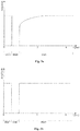
- Fig. 3a shows a signal course of a sensor signal of a movement sensor in a sensor system comprising a movement sensor and a touch sensor, wherein no measures for reducing the settling time of the movement sensor are provided.
- the sensor system is operated in the second mode of operation BM2.
- a switchover from a second mode of operation BM2 into the first mode of operation BM1 is carried out, in which the contacting of a sensor surface by an object is detected.
- a switchover from the first mode of operation BM1 into the second mode of operation BM2 is carried out.
- Fig. 3b shows the course of a signal of a sensor signal of a movement sensor in a sensor system comprising a touch sensor and a movement sensor, wherein the sensor system provides the measures for reducing the settling time of the movement sensor described with relation to Fig. 1 .
- the reduction according to the invention of the settling time of the capacitive movement sensor has the advantage that almost immediately after the switchover into the second mode of operation BM2 a settled sensor signal is present so that already immediately after the switchover of the mode of operation a movement detection may be carried out without additional measures having to be provided, as it would be the case with a signal course according to Fig. 3a , for example.
- the sensor system according to the invention and the method according to the invention for reducing the settling time of the sensor signal of the movement sensor in addition have the advantage that noise in the sensor signal of the movement sensor is reduced significantly.
- a further advantage is that the signal processing is simplified considerably, because an extensive signal processing of the settling and not yet settled signal, respectively, may be forgone, so that more time and more calculating time, respectively, is available for other applications.
- the precision of detection of the movement detection may be improved significantly, because potential inaccuracies in the movement detection are eliminated to the greatest possible extent by means of the reduction of the settling time.
- the sensor system according to the invention may be used in devices, in particular electric handheld devices, which comprise a touch sensitive and approach sensitive input surface, for example a touch panel.
- the electric handheld device may be a mobile cell phone, a cordless telephone, a mobile mini-computer, a tablet PC or the like.
- the touch sensor often only is an integrated circuit IC or a single chip system SoC, in which internal structures may be switched on and off.
- other measures may be provided to suppress the temporal variation of the pin capacitance, for example suitable transistor circuits and transistor devices, respectively.
Claims (15)
- Sensorsystem (1), das eine erste Sensoranordnung (10) mit einer mit mehreren ersten Sensorelektroden (11) verbundenen Berührungssteuerung und eine zweite kapazitive Sensoranordnung (20) aufweist, die eine kapazitive berührungslose Bewegungssteuerung aufweist, die mit einer Vielzahl von zweiten kapazitiven Sensorelektroden (21) verbunden ist, die konfiguriert sind, um eine Bewegung eines Objekts relativ zu einer Detektionsfläche zu erfassen, wobei eine der ersten Sensorelektroden (11) und eine der zweiten kapazitiven Sensorelektroden (21) so angeordnet sind, dass sie einen Abstand voneinander aufweisen, der eine kapazitive Kopplung (CPATH) definiert, wobei das Sensorsystem (1) in einem ersten Betriebsmodus (BM1) unter Verwendung der ersten Sensoranordnung und in einem zweiten Betriebsmodus (BM2) unter Verwendung der zweiten kapazitive Sensoranordnung (20) betrieben werden kann, wobei das Sensorsystem (1) konfiguriert ist, von der ersten Betriebsart in die zweite Betriebsart umgeschaltet zu werden, und wobei, wenn es von der ersten Betriebsart in die zweite Betriebsart umgeschaltet wird, während es sich in der zweiten Betriebsart befindet, die eine der zweiten kapazitiven Sensorelektroden (21) mit einem Sensoreingang der kapazitiven berührungslosen Bewegungssteuerung verbunden ist und die eine der ersten Sensorelektroden (11) mit einem Sensoreingang des Touch-Controllers verbunden ist, wobei die erste Sensoranordnung (10) mindestens einen Signalpfad aufweist, der mit einem vorgegebenen festen elektrischen Potential (40) verbunden ist, das parallel zu einer parasitären Kapazität (CPARA) der ersten Sensoranordnung (10) ist, wobei die parasitäre Kapazität (CPARA) zwischen einem Verbindungsknoten der Steuerung, die mit der einen der ersten Sensorelektroden (11) verbunden ist, und dem vorgegebenen festen elektrischen Potential (40) verbunden ist.
- Sensorsystem nach Anspruch 1, wobei das vorgegebene feste elektrische Potential (40) zumindest eines von Massepotential (GND), Versorgungsspannung (Vcc), der Hälfte der Versorgungsspannung (Vcc / 2) und einem elektrischen Potential zwischen Massepotential (GND) und Versorgungsspannung (Vcc) aufweist.
- Sensorsystem nach Anspruch 1 oder 2, wobei der Signalpfad über einen elektrischen Widerstand RBYPASS mit dem vorgegebenen elektrischen Potential (40) verbunden ist.
- Sensorsystem nach Anspruch 3, wobei mittels des Signalpfads zumindest ein mit dem Verbindungsknoten der ersten Sensoranordnung (10) verbundener Anschluss (PIN) über den elektrischen Widerstand (RBYPASS) mit dem vorgegebenen elektrischen Potential (40) gekoppelt ist.
- Sensorsystem nach einem der vorhergehenden Ansprüche, wobei die erste Sensoranordnung (10) eine kapazitive Sensoranordnung zum Erfassen eines Kontakts durch ein Objekt mit einer Detektionsfläche ist, wobei in der ersten Betriebsart (BM1) ein Kontakt des Objekts mit einer der kapazitiven Sensorelektroden (11) detektiert wird, und wobei in der zweiten Betriebsart (BM2) die Bewegung des Objekts detektiert wird.
- Sensorsystem nach Anspruch 5, wobei mittels des Signalpfads zumindest eine Elektrode (11) der ersten Sensoranordnung (10) über den elektrischen Widerstand (RBYPASS) mit dem vorgegebenen elektrischen Potential (40) gekoppelt ist.
- Sensorsystem nach Anspruch 5, wobei jede Elektrode der Vielzahl von ersten Elektroden (11) in einem jeweiligen Abstand von der zweiten kapazitiven Sensorelektrode (21) angeordnet ist, wobei- zumindest diese ersten Sensorelektroden (11) jeweils über einen elektrischen Widerstand (RBYPASS) mit dem vorgegebenen elektrischen Potential (40) gekoppelt sind, dessen Abstand von der zweiten Sensorelektrode (11) unter einem vorgegebenen Wert liegt.
- Sensorsystem nach einem der vorhergehenden Ansprüche, wobei in dem Signalpfad eine Schalteinrichtung (50) vorgesehen ist, die dazu ausgelegt ist, den Signalpfad in der zweiten Betriebsart (BM2) mit dem vorgegebenen festen elektrischen Potential (40) zu verbinden.
- Verfahren zum Betreiben eines Sensorsystems nach einem der vorhergehenden Ansprüche zum Reduzieren einer Einschwingzeit der zweiten kapazitiven Sensoranordnung (20), wobei das Verfahren aufweist:Betreiben des Sensorsystems (1) in der ersten Betriebsart;Umschalten des Sensorsystems von der ersten Betriebsart in die zweite Betriebsart, wobei der zumindest eine Signalpfad mit dem vorgegebenen festen elektrischen Potential (40) verbunden ist, undBetreiben des Sensorsystems (1) in der zweiten Betriebsart.
- Verfahren nach Anspruch 9, wobei der Signalpfad über einen elektrischen Widerstand (RBYPASS) mit dem vorgegebenen elektrischen Potential (40) verbunden ist.
- Verfahren nach einem der Ansprüche 9 oder 10, wobei der Schritt des Verbindens des zumindest einen Signalpfads durch eine permanente Verbindung über den elektrischen Widerstand (RBYPASS) bereitgestellt wird.
- Verfahren nach einem der Ansprüche 9 oder 10, wobei der Schritt des Verbindens des zumindest einen Signalpfads durch Steuern eines Schalters (50) bereitgestellt wird, der zwischen dem Signalpfad und dem vorgegebenen festen elektrischen Potential (40) angeschlossen ist.
- Verfahren nach einem der vorhergehenden Ansprüche 9 bis 12, wobei in der ersten Betriebsart (BM1) ein Kontakt detektiert wird und in der zweiten Betriebsart (BM2) die Bewegung detektiert wird.
- Verfahren nach Anspruch 13, das aufweist:- Verbinden zumindest eines Anschlusses (PIN) der ersten kapazitiven Sensoranordnung (10) mit dem Verbindungsknoten mit dem vorgegebenen elektrischen Potential (40) über den elektrischen Widerstand (RBYPASS).
- Verfahren nach einem der vorhergehenden Ansprüche 9 bis 14, wobei jede Elektrode der Vielzahl von ersten Elektroden in einem jeweiligen Abstand von dem zweiten kapazitiven Sensor (21) angeordnet ist, wobei das Verfahren weiterhin aufweist:- Koppeln zumindest dieser ersten Sensorelektroden (11) über einen jeweiligen elektrischen Widerstand (RBYPASS) mit dem vorgegebenen elektrischen Potential (40), dessen Abstand von der zweiten Sensorelektrode (11) unter einem vorgegebenen Wert liegt.
Applications Claiming Priority (2)
| Application Number | Priority Date | Filing Date | Title |
|---|---|---|---|
| DE102011056226A DE102011056226A1 (de) | 2011-12-09 | 2011-12-09 | Sensorsystem sowie Verfahren zur Reduktion einer Einschwingzeit eines Sensorsystems |
| PCT/EP2012/074717 WO2013083736A1 (en) | 2011-12-09 | 2012-12-06 | Sensor system and method for reducing a settling time of a sensor system |
Publications (2)
| Publication Number | Publication Date |
|---|---|
| EP2789100A1 EP2789100A1 (de) | 2014-10-15 |
| EP2789100B1 true EP2789100B1 (de) | 2020-03-25 |
Family
ID=47522488
Family Applications (1)
| Application Number | Title | Priority Date | Filing Date |
|---|---|---|---|
| EP12812893.1A Active EP2789100B1 (de) | 2011-12-09 | 2012-12-06 | Sensorsystem und verfahren zur verringerung der einschwingzeit eines sensorsystems |
Country Status (8)
| Country | Link |
|---|---|
| US (1) | US9476924B2 (de) |
| EP (1) | EP2789100B1 (de) |
| JP (1) | JP6035344B2 (de) |
| KR (1) | KR102000218B1 (de) |
| CN (1) | CN103975529B (de) |
| DE (1) | DE102011056226A1 (de) |
| TW (1) | TWI588490B (de) |
| WO (1) | WO2013083736A1 (de) |
Families Citing this family (4)
| Publication number | Priority date | Publication date | Assignee | Title |
|---|---|---|---|---|
| DE102011056226A1 (de) | 2011-12-09 | 2013-06-13 | Ident Technology Ag | Sensorsystem sowie Verfahren zur Reduktion einer Einschwingzeit eines Sensorsystems |
| GB2518871A (en) * | 2013-10-03 | 2015-04-08 | Nokia Technologies Oy | Sensing |
| FR3060734B1 (fr) * | 2016-12-16 | 2019-01-25 | Fogale Nanotech | Dispositif et procede de detection de l'approche et/ou de contact, et de l'appui d'un objet, relativement a une surface de detection |
| FR3060733B1 (fr) * | 2016-12-16 | 2019-01-25 | Fogale Nanotech | Dispositif et procede de detection de l'approche et/ou de contact, et de l'appui d'un objet, relativement a une surface de detection |
Family Cites Families (17)
| Publication number | Priority date | Publication date | Assignee | Title |
|---|---|---|---|---|
| US5543591A (en) | 1992-06-08 | 1996-08-06 | Synaptics, Incorporated | Object position detector with edge motion feature and gesture recognition |
| JP4287130B2 (ja) * | 2002-12-05 | 2009-07-01 | 東京エレクトロン株式会社 | 静電容量検出回路及び静電容量検出方法 |
| JP2004317403A (ja) * | 2003-04-18 | 2004-11-11 | Alps Electric Co Ltd | 面圧分布センサ |
| US7902842B2 (en) | 2005-06-03 | 2011-03-08 | Synaptics Incorporated | Methods and systems for switched charge transfer capacitance measuring using shared components |
| JP2007178420A (ja) * | 2005-11-30 | 2007-07-12 | Denso Corp | 容量式物理量センサおよびその診断方法 |
| US20080202251A1 (en) * | 2007-02-27 | 2008-08-28 | Iee International Electronics & Engineering S.A. | Capacitive pressure sensor |
| US8860683B2 (en) * | 2007-04-05 | 2014-10-14 | Cypress Semiconductor Corporation | Integrated button activation sensing and proximity sensing |
| US7583092B2 (en) | 2007-07-30 | 2009-09-01 | Synaptics Incorporated | Capacitive sensing apparatus that uses a combined guard and sensing electrode |
| US8115499B2 (en) * | 2009-05-22 | 2012-02-14 | Freescale Semiconductor, Inc. | Device with proximity detection capability |
| JP5548270B2 (ja) * | 2009-08-21 | 2014-07-16 | アップル インコーポレイテッド | 容量性感知方法及び装置 |
| CN102597931B (zh) * | 2009-11-09 | 2016-01-27 | 罗姆股份有限公司 | 带触摸传感器的显示器、控制电路和使用它的电子设备 |
| DE102009055143A1 (de) * | 2009-12-22 | 2011-06-30 | BSH Bosch und Siemens Hausgeräte GmbH, 81739 | Berührungsempfindlicher Taster |
| JP2011170616A (ja) | 2010-02-18 | 2011-09-01 | On Semiconductor Trading Ltd | 静電容量型タッチセンサ |
| US8736283B2 (en) | 2010-03-04 | 2014-05-27 | Franklin Sensors Inc. | Advanced obscured feature detector |
| CN102859477B (zh) * | 2010-04-16 | 2016-11-16 | 微晶片科技德国公司 | Tft显示器、oled接口及用于在安置于显示器上游的空间区域中检测边沿的空间位置的方法 |
| US8717331B2 (en) * | 2010-08-24 | 2014-05-06 | Cypress Semiconductor Corporation | Reducing water influence on a touch-sensing device |
| DE102011056226A1 (de) | 2011-12-09 | 2013-06-13 | Ident Technology Ag | Sensorsystem sowie Verfahren zur Reduktion einer Einschwingzeit eines Sensorsystems |
-
2011
- 2011-12-09 DE DE102011056226A patent/DE102011056226A1/de not_active Ceased
-
2012
- 2012-12-06 US US14/363,938 patent/US9476924B2/en active Active
- 2012-12-06 WO PCT/EP2012/074717 patent/WO2013083736A1/en active Application Filing
- 2012-12-06 KR KR1020147019090A patent/KR102000218B1/ko active IP Right Grant
- 2012-12-06 CN CN201280060739.0A patent/CN103975529B/zh not_active Expired - Fee Related
- 2012-12-06 EP EP12812893.1A patent/EP2789100B1/de active Active
- 2012-12-06 JP JP2014545269A patent/JP6035344B2/ja not_active Expired - Fee Related
- 2012-12-07 TW TW101146256A patent/TWI588490B/zh not_active IP Right Cessation
Non-Patent Citations (1)
| Title |
|---|
| None * |
Also Published As
| Publication number | Publication date |
|---|---|
| DE102011056226A1 (de) | 2013-06-13 |
| KR20140109946A (ko) | 2014-09-16 |
| TW201337270A (zh) | 2013-09-16 |
| CN103975529A (zh) | 2014-08-06 |
| TWI588490B (zh) | 2017-06-21 |
| WO2013083736A1 (en) | 2013-06-13 |
| JP2015505081A (ja) | 2015-02-16 |
| JP6035344B2 (ja) | 2016-11-30 |
| US9476924B2 (en) | 2016-10-25 |
| EP2789100A1 (de) | 2014-10-15 |
| CN103975529B (zh) | 2017-09-01 |
| KR102000218B1 (ko) | 2019-07-15 |
| US20150097585A1 (en) | 2015-04-09 |
Similar Documents
| Publication | Publication Date | Title |
|---|---|---|
| US10191588B2 (en) | Coordinate input device and display device with the same | |
| US8339139B2 (en) | System and method for testing a circuit | |
| EP3640779B1 (de) | Schaltung, berührungschip und elektronische vorrichtung zur kapazitätserkennung | |
| US9652104B2 (en) | Capacitance voltage conversion circuit, input apparatus using the same, electronic instrument, and capacitance voltage conversion method | |
| US9678597B2 (en) | Signal processing circuit, signal processing method, position detector, and electronic device for position detection sensor including sensor self-capacitance correction | |
| EP2789100B1 (de) | Sensorsystem und verfahren zur verringerung der einschwingzeit eines sensorsystems | |
| US9041671B2 (en) | Adaptive touch sensor control based on identification of attached accessory | |
| US20160188949A1 (en) | Fingerprint sensing device and fingerprint sensing method thereof | |
| KR20060008984A (ko) | 전기장 물체 감지 시스템, 전자 제품용 제어 회로 및 출력제공 방법 | |
| WO2002063323A3 (en) | Method and apparatus for contactless capacitive testing of integrated circuits | |
| CN110300897A (zh) | 电容检测电路、触控装置和终端设备 | |
| WO2016107910A1 (en) | Capacitive sensor | |
| TW201337279A (zh) | 電容偵測裝置及應用該電容偵測裝置之電容式觸控系統 | |
| JP2020086743A (ja) | タッチ検出回路、入力装置、電子機器 | |
| KR101733740B1 (ko) | 배터리 보호 회로 | |
| WO2008105234A1 (ja) | 静電容量変化検出回路及び半導体装置 | |
| EP2341626B1 (de) | Kommunikationszelle für eine integrierte Schaltung, Chip mit der Kommunikationszelle, elektronisches System mit dem Chip und Prüfvorrichtung | |
| KR101041586B1 (ko) | 터치센서의 커패시턴스 직·간접 적분회로 | |
| US9329736B2 (en) | Capacitive touch panel input device that measures internal resistances for compensation | |
| CN111492580A (zh) | 一种无线接收电路中mos管的过压防护电路 | |
| CN113671232A (zh) | 一种剩余电流检测装置 |
Legal Events
| Date | Code | Title | Description |
|---|---|---|---|
| PUAI | Public reference made under article 153(3) epc to a published international application that has entered the european phase |
Free format text: ORIGINAL CODE: 0009012 |
|
| 17P | Request for examination filed |
Effective date: 20140708 |
|
| AK | Designated contracting states |
Kind code of ref document: A1 Designated state(s): AL AT BE BG CH CY CZ DE DK EE ES FI FR GB GR HR HU IE IS IT LI LT LU LV MC MK MT NL NO PL PT RO RS SE SI SK SM TR |
|
| DAX | Request for extension of the european patent (deleted) | ||
| STAA | Information on the status of an ep patent application or granted ep patent |
Free format text: STATUS: EXAMINATION IS IN PROGRESS |
|
| 17Q | First examination report despatched |
Effective date: 20170714 |
|
| RAP1 | Party data changed (applicant data changed or rights of an application transferred) |
Owner name: MICROCHIP TECHNOLOGY GERMANY GMBH |
|
| GRAP | Despatch of communication of intention to grant a patent |
Free format text: ORIGINAL CODE: EPIDOSNIGR1 |
|
| STAA | Information on the status of an ep patent application or granted ep patent |
Free format text: STATUS: GRANT OF PATENT IS INTENDED |
|
| INTG | Intention to grant announced |
Effective date: 20191025 |
|
| GRAS | Grant fee paid |
Free format text: ORIGINAL CODE: EPIDOSNIGR3 |
|
| GRAA | (expected) grant |
Free format text: ORIGINAL CODE: 0009210 |
|
| STAA | Information on the status of an ep patent application or granted ep patent |
Free format text: STATUS: THE PATENT HAS BEEN GRANTED |
|
| AK | Designated contracting states |
Kind code of ref document: B1 Designated state(s): AL AT BE BG CH CY CZ DE DK EE ES FI FR GB GR HR HU IE IS IT LI LT LU LV MC MK MT NL NO PL PT RO RS SE SI SK SM TR |
|
| REG | Reference to a national code |
Ref country code: GB Ref legal event code: FG4D |
|
| REG | Reference to a national code |
Ref country code: AT Ref legal event code: REF Ref document number: 1249765 Country of ref document: AT Kind code of ref document: T Effective date: 20200415 Ref country code: IE Ref legal event code: FG4D |
|
| REG | Reference to a national code |
Ref country code: DE Ref legal event code: R096 Ref document number: 602012068779 Country of ref document: DE |
|
| PG25 | Lapsed in a contracting state [announced via postgrant information from national office to epo] |
Ref country code: RS Free format text: LAPSE BECAUSE OF FAILURE TO SUBMIT A TRANSLATION OF THE DESCRIPTION OR TO PAY THE FEE WITHIN THE PRESCRIBED TIME-LIMIT Effective date: 20200325 Ref country code: FI Free format text: LAPSE BECAUSE OF FAILURE TO SUBMIT A TRANSLATION OF THE DESCRIPTION OR TO PAY THE FEE WITHIN THE PRESCRIBED TIME-LIMIT Effective date: 20200325 Ref country code: NO Free format text: LAPSE BECAUSE OF FAILURE TO SUBMIT A TRANSLATION OF THE DESCRIPTION OR TO PAY THE FEE WITHIN THE PRESCRIBED TIME-LIMIT Effective date: 20200625 |
|
| PG25 | Lapsed in a contracting state [announced via postgrant information from national office to epo] |
Ref country code: GR Free format text: LAPSE BECAUSE OF FAILURE TO SUBMIT A TRANSLATION OF THE DESCRIPTION OR TO PAY THE FEE WITHIN THE PRESCRIBED TIME-LIMIT Effective date: 20200626 Ref country code: BG Free format text: LAPSE BECAUSE OF FAILURE TO SUBMIT A TRANSLATION OF THE DESCRIPTION OR TO PAY THE FEE WITHIN THE PRESCRIBED TIME-LIMIT Effective date: 20200625 Ref country code: LV Free format text: LAPSE BECAUSE OF FAILURE TO SUBMIT A TRANSLATION OF THE DESCRIPTION OR TO PAY THE FEE WITHIN THE PRESCRIBED TIME-LIMIT Effective date: 20200325 Ref country code: SE Free format text: LAPSE BECAUSE OF FAILURE TO SUBMIT A TRANSLATION OF THE DESCRIPTION OR TO PAY THE FEE WITHIN THE PRESCRIBED TIME-LIMIT Effective date: 20200325 Ref country code: HR Free format text: LAPSE BECAUSE OF FAILURE TO SUBMIT A TRANSLATION OF THE DESCRIPTION OR TO PAY THE FEE WITHIN THE PRESCRIBED TIME-LIMIT Effective date: 20200325 |
|
| REG | Reference to a national code |
Ref country code: NL Ref legal event code: MP Effective date: 20200325 |
|
| REG | Reference to a national code |
Ref country code: LT Ref legal event code: MG4D |
|
| PG25 | Lapsed in a contracting state [announced via postgrant information from national office to epo] |
Ref country code: NL Free format text: LAPSE BECAUSE OF FAILURE TO SUBMIT A TRANSLATION OF THE DESCRIPTION OR TO PAY THE FEE WITHIN THE PRESCRIBED TIME-LIMIT Effective date: 20200325 |
|
| PG25 | Lapsed in a contracting state [announced via postgrant information from national office to epo] |
Ref country code: LT Free format text: LAPSE BECAUSE OF FAILURE TO SUBMIT A TRANSLATION OF THE DESCRIPTION OR TO PAY THE FEE WITHIN THE PRESCRIBED TIME-LIMIT Effective date: 20200325 Ref country code: EE Free format text: LAPSE BECAUSE OF FAILURE TO SUBMIT A TRANSLATION OF THE DESCRIPTION OR TO PAY THE FEE WITHIN THE PRESCRIBED TIME-LIMIT Effective date: 20200325 Ref country code: SM Free format text: LAPSE BECAUSE OF FAILURE TO SUBMIT A TRANSLATION OF THE DESCRIPTION OR TO PAY THE FEE WITHIN THE PRESCRIBED TIME-LIMIT Effective date: 20200325 Ref country code: PT Free format text: LAPSE BECAUSE OF FAILURE TO SUBMIT A TRANSLATION OF THE DESCRIPTION OR TO PAY THE FEE WITHIN THE PRESCRIBED TIME-LIMIT Effective date: 20200818 Ref country code: SK Free format text: LAPSE BECAUSE OF FAILURE TO SUBMIT A TRANSLATION OF THE DESCRIPTION OR TO PAY THE FEE WITHIN THE PRESCRIBED TIME-LIMIT Effective date: 20200325 Ref country code: IS Free format text: LAPSE BECAUSE OF FAILURE TO SUBMIT A TRANSLATION OF THE DESCRIPTION OR TO PAY THE FEE WITHIN THE PRESCRIBED TIME-LIMIT Effective date: 20200725 Ref country code: CZ Free format text: LAPSE BECAUSE OF FAILURE TO SUBMIT A TRANSLATION OF THE DESCRIPTION OR TO PAY THE FEE WITHIN THE PRESCRIBED TIME-LIMIT Effective date: 20200325 Ref country code: RO Free format text: LAPSE BECAUSE OF FAILURE TO SUBMIT A TRANSLATION OF THE DESCRIPTION OR TO PAY THE FEE WITHIN THE PRESCRIBED TIME-LIMIT Effective date: 20200325 |
|
| REG | Reference to a national code |
Ref country code: AT Ref legal event code: MK05 Ref document number: 1249765 Country of ref document: AT Kind code of ref document: T Effective date: 20200325 |
|
| REG | Reference to a national code |
Ref country code: DE Ref legal event code: R097 Ref document number: 602012068779 Country of ref document: DE |
|
| PG25 | Lapsed in a contracting state [announced via postgrant information from national office to epo] |
Ref country code: ES Free format text: LAPSE BECAUSE OF FAILURE TO SUBMIT A TRANSLATION OF THE DESCRIPTION OR TO PAY THE FEE WITHIN THE PRESCRIBED TIME-LIMIT Effective date: 20200325 Ref country code: IT Free format text: LAPSE BECAUSE OF FAILURE TO SUBMIT A TRANSLATION OF THE DESCRIPTION OR TO PAY THE FEE WITHIN THE PRESCRIBED TIME-LIMIT Effective date: 20200325 Ref country code: DK Free format text: LAPSE BECAUSE OF FAILURE TO SUBMIT A TRANSLATION OF THE DESCRIPTION OR TO PAY THE FEE WITHIN THE PRESCRIBED TIME-LIMIT Effective date: 20200325 Ref country code: AT Free format text: LAPSE BECAUSE OF FAILURE TO SUBMIT A TRANSLATION OF THE DESCRIPTION OR TO PAY THE FEE WITHIN THE PRESCRIBED TIME-LIMIT Effective date: 20200325 |
|
| PLBE | No opposition filed within time limit |
Free format text: ORIGINAL CODE: 0009261 |
|
| STAA | Information on the status of an ep patent application or granted ep patent |
Free format text: STATUS: NO OPPOSITION FILED WITHIN TIME LIMIT |
|
| PG25 | Lapsed in a contracting state [announced via postgrant information from national office to epo] |
Ref country code: PL Free format text: LAPSE BECAUSE OF FAILURE TO SUBMIT A TRANSLATION OF THE DESCRIPTION OR TO PAY THE FEE WITHIN THE PRESCRIBED TIME-LIMIT Effective date: 20200325 |
|
| 26N | No opposition filed |
Effective date: 20210112 |
|
| PG25 | Lapsed in a contracting state [announced via postgrant information from national office to epo] |
Ref country code: SI Free format text: LAPSE BECAUSE OF FAILURE TO SUBMIT A TRANSLATION OF THE DESCRIPTION OR TO PAY THE FEE WITHIN THE PRESCRIBED TIME-LIMIT Effective date: 20200325 |
|
| REG | Reference to a national code |
Ref country code: CH Ref legal event code: PL |
|
| GBPC | Gb: european patent ceased through non-payment of renewal fee |
Effective date: 20201206 |
|
| PG25 | Lapsed in a contracting state [announced via postgrant information from national office to epo] |
Ref country code: MC Free format text: LAPSE BECAUSE OF FAILURE TO SUBMIT A TRANSLATION OF THE DESCRIPTION OR TO PAY THE FEE WITHIN THE PRESCRIBED TIME-LIMIT Effective date: 20200325 |
|
| REG | Reference to a national code |
Ref country code: BE Ref legal event code: MM Effective date: 20201231 |
|
| PG25 | Lapsed in a contracting state [announced via postgrant information from national office to epo] |
Ref country code: FR Free format text: LAPSE BECAUSE OF NON-PAYMENT OF DUE FEES Effective date: 20201231 Ref country code: LU Free format text: LAPSE BECAUSE OF NON-PAYMENT OF DUE FEES Effective date: 20201206 Ref country code: IE Free format text: LAPSE BECAUSE OF NON-PAYMENT OF DUE FEES Effective date: 20201206 |
|
| PG25 | Lapsed in a contracting state [announced via postgrant information from national office to epo] |
Ref country code: CH Free format text: LAPSE BECAUSE OF NON-PAYMENT OF DUE FEES Effective date: 20201231 Ref country code: GB Free format text: LAPSE BECAUSE OF NON-PAYMENT OF DUE FEES Effective date: 20201206 Ref country code: LI Free format text: LAPSE BECAUSE OF NON-PAYMENT OF DUE FEES Effective date: 20201231 |
|
| PGFP | Annual fee paid to national office [announced via postgrant information from national office to epo] |
Ref country code: DE Payment date: 20211117 Year of fee payment: 10 |
|
| PG25 | Lapsed in a contracting state [announced via postgrant information from national office to epo] |
Ref country code: TR Free format text: LAPSE BECAUSE OF FAILURE TO SUBMIT A TRANSLATION OF THE DESCRIPTION OR TO PAY THE FEE WITHIN THE PRESCRIBED TIME-LIMIT Effective date: 20200325 Ref country code: MT Free format text: LAPSE BECAUSE OF FAILURE TO SUBMIT A TRANSLATION OF THE DESCRIPTION OR TO PAY THE FEE WITHIN THE PRESCRIBED TIME-LIMIT Effective date: 20200325 Ref country code: CY Free format text: LAPSE BECAUSE OF FAILURE TO SUBMIT A TRANSLATION OF THE DESCRIPTION OR TO PAY THE FEE WITHIN THE PRESCRIBED TIME-LIMIT Effective date: 20200325 |
|
| PG25 | Lapsed in a contracting state [announced via postgrant information from national office to epo] |
Ref country code: MK Free format text: LAPSE BECAUSE OF FAILURE TO SUBMIT A TRANSLATION OF THE DESCRIPTION OR TO PAY THE FEE WITHIN THE PRESCRIBED TIME-LIMIT Effective date: 20200325 Ref country code: AL Free format text: LAPSE BECAUSE OF FAILURE TO SUBMIT A TRANSLATION OF THE DESCRIPTION OR TO PAY THE FEE WITHIN THE PRESCRIBED TIME-LIMIT Effective date: 20200325 |
|
| PG25 | Lapsed in a contracting state [announced via postgrant information from national office to epo] |
Ref country code: BE Free format text: LAPSE BECAUSE OF NON-PAYMENT OF DUE FEES Effective date: 20201231 |
|
| REG | Reference to a national code |
Ref country code: DE Ref legal event code: R119 Ref document number: 602012068779 Country of ref document: DE |
|
| PG25 | Lapsed in a contracting state [announced via postgrant information from national office to epo] |
Ref country code: DE Free format text: LAPSE BECAUSE OF NON-PAYMENT OF DUE FEES Effective date: 20230701 |