EP2789084B1 - Method for operating a power converter module and a device therefor - Google Patents
Method for operating a power converter module and a device therefor Download PDFInfo
- Publication number
- EP2789084B1 EP2789084B1 EP11805667.0A EP11805667A EP2789084B1 EP 2789084 B1 EP2789084 B1 EP 2789084B1 EP 11805667 A EP11805667 A EP 11805667A EP 2789084 B1 EP2789084 B1 EP 2789084B1
- Authority
- EP
- European Patent Office
- Prior art keywords
- output
- power converter
- voltage
- converter module
- circuitry
- Prior art date
- Legal status (The legal status is an assumption and is not a legal conclusion. Google has not performed a legal analysis and makes no representation as to the accuracy of the status listed.)
- Not-in-force
Links
- 238000000034 method Methods 0.000 title claims description 55
- 238000012545 processing Methods 0.000 claims description 31
- 230000003044 adaptive effect Effects 0.000 claims description 16
- 230000004044 response Effects 0.000 claims 1
- 101150090128 PCM1 gene Proteins 0.000 description 50
- 238000010586 diagram Methods 0.000 description 19
- 238000005457 optimization Methods 0.000 description 6
- 238000006243 chemical reaction Methods 0.000 description 4
- 238000012544 monitoring process Methods 0.000 description 4
- 238000004891 communication Methods 0.000 description 3
- 230000007423 decrease Effects 0.000 description 3
- 230000004913 activation Effects 0.000 description 2
- 238000001994 activation Methods 0.000 description 2
- 230000005540 biological transmission Effects 0.000 description 2
- 239000003990 capacitor Substances 0.000 description 2
- 230000003247 decreasing effect Effects 0.000 description 2
- 238000004519 manufacturing process Methods 0.000 description 2
- 238000007599 discharging Methods 0.000 description 1
- 230000000977 initiatory effect Effects 0.000 description 1
- 238000005259 measurement Methods 0.000 description 1
- 230000003442 weekly effect Effects 0.000 description 1
Images


Classifications
-
- H—ELECTRICITY
- H02—GENERATION; CONVERSION OR DISTRIBUTION OF ELECTRIC POWER
- H02M—APPARATUS FOR CONVERSION BETWEEN AC AND AC, BETWEEN AC AND DC, OR BETWEEN DC AND DC, AND FOR USE WITH MAINS OR SIMILAR POWER SUPPLY SYSTEMS; CONVERSION OF DC OR AC INPUT POWER INTO SURGE OUTPUT POWER; CONTROL OR REGULATION THEREOF
- H02M1/00—Details of apparatus for conversion
- H02M1/32—Means for protecting converters other than automatic disconnection
-
- G—PHYSICS
- G05—CONTROLLING; REGULATING
- G05F—SYSTEMS FOR REGULATING ELECTRIC OR MAGNETIC VARIABLES
- G05F1/00—Automatic systems in which deviations of an electric quantity from one or more predetermined values are detected at the output of the system and fed back to a device within the system to restore the detected quantity to its predetermined value or values, i.e. retroactive systems
- G05F1/10—Regulating voltage or current
- G05F1/46—Regulating voltage or current wherein the variable actually regulated by the final control device is DC
- G05F1/56—Regulating voltage or current wherein the variable actually regulated by the final control device is DC using semiconductor devices in series with the load as final control devices
-
- H—ELECTRICITY
- H02—GENERATION; CONVERSION OR DISTRIBUTION OF ELECTRIC POWER
- H02M—APPARATUS FOR CONVERSION BETWEEN AC AND AC, BETWEEN AC AND DC, OR BETWEEN DC AND DC, AND FOR USE WITH MAINS OR SIMILAR POWER SUPPLY SYSTEMS; CONVERSION OF DC OR AC INPUT POWER INTO SURGE OUTPUT POWER; CONTROL OR REGULATION THEREOF
- H02M1/00—Details of apparatus for conversion
- H02M1/0003—Details of control, feedback or regulation circuits
Definitions
- the embodiments described herein relate to a method for operating a power converter module and in particular to a method for operating a power converter module with increased power density.
- a simple switched mode voltage converter comprises an input voltage terminal, an externally controlled switch, an inductor, a capacitor and a diode.
- the basic principle of such a switched mode voltage converter is that by means of the externally controlled switch the charging and discharging of the capacitor and the inductor is controlled and used for the conversion of the input voltage at the input terminal. If the external switch is efficient in terms of switching time and other losses the switched mode voltage converter becomes very efficient. However, some components of the voltage converter usually exhibit some losses, for example the core of the inductor imposes some limitations on the voltage conversion due to magnetic saturation thereof. Also the externally controlled switch that often comprises a MOSFET transistor imposes some limits on the maximum allowed switching voltage and current.
- switched mode voltage converter is a "buck" converter for down conversion of the input voltage.
- Such switched mode voltage converters are efficient and needs a minimum of large passive components compared to the older linear types of voltage regulators.
- Adaptive bus voltage is implemented by having a first controllable power converter that feeds an intermediate bus voltage to a second power converter used for supplying the load with power.
- the first power converter adjusts the intermediate bus voltage to match the load of the system.
- the power converters are not allowed to operate in a more optimum way.
- the intermediate bus voltage is not allowed to be adjusted to such low levels that the actual load of the power converter suggests.
- the power converter is not allowed to operate using the optimum bus voltage.
- Patent document US 2005/190517 A1 discloses a method for operating a power converter module, the power converter module comprising: An input terminal and an output terminal, a voltage converter having an input side operatively connected to the input terminal, and an output side operatively connected to an output circuitry, the output circuitry is further operatively connected to the output terminal, and operable for measuring output parameters at the output terminal of the power converter module, the power converter module further comprising a processing circuitry operatively connected to the voltage converter and to the output circuitry, and operable for controlling the voltage converter, the method comprising transmitting a status signal representing the operating parameters of the output circuitry to the processing circuitry.
- US 2005/190517 A1 discloses to reduce overdimensioning with a thermal model that uses either output parameters OR measured temperature values.
- a first exemplary embodiment provides a method for operating a power converter module.
- the power converter module comprises an input terminal and an output terminal, and a voltage converter having an input side and an output side.
- the input side of the voltage converter is operatively connected to the input terminal of the power converter.
- the output side of the voltage converter is operatively connected to an output circuitry.
- the output circuitry is operable for measuring output parameters at the output terminal of the power converter module.
- the power converter module further comprises a processing circuitry, which is operable for controlling the voltage converter.
- the method comprises a step of transmitting a first status signal representing operating parameters of the voltage converter to the processing circuitry.
- the method also comprises a step of determining whether the status of the voltage converter is acceptable or unacceptable.
- a second status signal is transmitted to the processing circuitry.
- the second status signal represents the operating parameters of the output circuitry.
- the method also comprises determining if the second status signal is above a predetermined threshold value.
- a peak output mode is entered according to the method. The peak output mode involves: determining based on a maximum output voltage if the output voltage at the output terminal is allowed to increase, increasing the output voltage if the output voltage at the output terminal is allowed to increase, and operating the voltage converter at maximum power dissipation as long as the status of the voltage converter is acceptable and the second status signal is above the predetermined threshold value.
- a second exemplary embodiment provides a power converter module.
- the power converter module comprises an input terminal and an output terminal, and a voltage converter having an input side and an output side.
- the input side is operatively connected to the input terminal of the power converter.
- the output side is operatively connected to an output circuitry.
- the output circuitry is operable for measuring output parameters at the output terminal of the power converter module.
- the power converter module further comprises a processing circuitry, which is operable for controlling the voltage converter.
- the voltage converter is configured to transmit a first status signal representing operating parameters of the voltage converter to the processing circuitry.
- the processing circuitry is configured to determine whether the status of the voltage converter is acceptable or unacceptable.
- the output circuitry is configured to transmit a second status signal representing the operating parameters of the output circuitry to the processing circuitry.
- the processing circuitry is further configured to determine if the second status signal is above a predetermined threshold value, and control the power converter module to enter a peak output mode, if the second status signal is above said predetermined threshold value and the status of the voltage converter is acceptable.
- the peak output mode when executed involves determining based on a maximum output voltage if the output voltage at the output terminal is allowed to increase, increasing the output voltage if the output voltage at the output terminal is allowed to increase, and operating the voltage converter at maximum power dissipation as long as the status of the voltage converter is acceptable and the second status signal is above said predetermined threshold value.
- a third exemplary embodiment provides a power converter system that comprises said power converter module, at least one power supply unit having an input side and an output side.
- the input side of the at least one power supply unit is operatively connected to the output terminal of the power converter module.
- the output side of the at least one power supply unit is arranged to provide an output voltage to a load.
- the power converter system also comprises an external unit operatively connected to said power converter module and to said at least one power supply unit.
- An advantage of certain embodiments described herein is that a power converter module can safely operate at or above the maximum rating thereof.
- Another advantage of some embodiments described herein is that adaptive operation of the power converter module can be fully exploited.
- Yet another advantage of some embodiments described herein is that peak output mode allows less safety margins in the operation of the power converter module.
- a further advantage of some embodiments of this disclosure is that remote monitoring of the power converter module is allowed.
- a further advantage of some embodiments of this disclosure is that more power is available without changing the electronics.
- a further advantage of some embodiments of this disclosure is that with adaptive bus voltage some embodiments will reduce power consumption, increase lifetime and lower the cost as well as reducing the size.
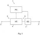
- Fig. 1 is a schematic block diagram of an exemplary power converter module (PCM) commonly designated 1, which comprises an input terminal 2 for connection of input voltage.
- the PCM 1 further comprises a voltage converter (VC) 4 with an input side 5 and an output side 6.
- the VC 4 is operable for converting the input voltage at the input terminal 2 to a different output voltage 3.
- the VC 4 comprises a regular voltage converter, for example a switched mode voltage converter of either "buck" or "boost" type or an AC/DC converter.
- Other types of voltage converters such as isolated converters of flyback, forward, push-pull, fullbridge and halfbridge type are of course also possible to use as VC 4.
- the input side 5 of the VC 4 is operatively connected to the input terminal 2 of the PCM 1 whereas the output side 6 of the VC 4 is operatively connected to an output circuitry (OC) 7.
- the OC 7 is operatively connected to the output terminal 3 and is operable for measuring output parameters at the output terminal 3 of the PCM 1, such output parameters can for example be output voltage and output current at the output terminal 3.
- the PCM 1 further comprises a processing circuitry (PC) 8 operable connected to the VC 4 and the OC 7.
- the PC 8 in this embodiment is operable for controlling the VC 4 and receiving said output parameters from the OC 7.
- the control signal from the PC 8 to the VC 4 preferably a pulse width modulated signal.
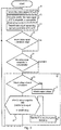
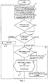
- Fig. 2 is a flow diagram of an exemplary method for operating a power converter according to embodiments of the invention. The method comprises:
- the fourth sub step 18 an additional step of operating the VC 4 at a higher current than the maximum current rating of the VC 4.
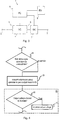
- Fig. 3 is a schematic block diagram of an exemplary PCM 1 comprising an external unit (EU) 9 operatively connected to the PC 8.
- EU 9 can for example be a controller that communicates with the PCM 1 for transmitting and receiving information about operating characteristics of the PCM 1.
- the EU 9 can be connected to the PCM 1 by means of a data bus, such as an I 2 C- or a CAN-bus.
- the hereinbefore described EU 9 comprises means for external communication such as a communication bus operatively connected to an external means for remote monitoring and/or control.
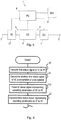
- Fig. 4 is a flow diagram of a method according to an alternative embodiment.
- the method comprises the first step 10 to the sixth step 15 as hereinbefore described with reference to Fig. 2 .
- the method comprises an additional step 21 of transmitting information about operation in peak output mode to the EU 9 in between the fifth step 14 and the sixth step 15.
- certain advantages occur, such as for example a possibility to monitor how many times the PCM 1 enters the peak output mode and/or how long the PCM 1 operated in the peak output mode. Such information can be valuable in order to assess estimated life time, warranty issues etc.
- the PC 8 of the PCM 1 comprises a computer readable memory and is operatively connected to the EU 9.
- This embodiment enables the PCM 1 to store information about the operation in peak output mode in the computer readable memory of the PC 8, wherein the step, as described with reference to Fig. 4 , of transmitting 21 the information about the operation in peak output mode 15 involves transmitting the information stored in the computer readable memory to the external unit 9.
- This embodiment allows, as an example, external polling of the information about the operation in peak output mode. Said polling can for example be performed remotely from the PCM 1 and wireless, thereby allowing an operator to continuously monitor the status of the PCM 1 remotely. Such monitoring can e.g. be useful for assessing estimated lifetime, warranty issues and optimization possibilities.
- the information stored in the computer readable memory can be accessed by the EU 9 at predetermined intervals such as monthly, weekly, daily, or at the time of entering the peak output mode.
- the PC 8 sends a signal to the EU 9 when a predetermined number of activations of peak output mode have been reached. This signal can then be used for initiating service, repair or replacement.
- a variant of the latter example is to have a predetermined time in peak output mode and when this time is lapsed the PC 8 sends a signal to the EU 9.
- Yet another variant is to disable peak output mode after a predetermined number of activations of peak output mode or alternatively after a predetermined time in peak output mode.
- Yet another embodiment of the method, described with reference to Fig. 4 is to store the information about entering peak output mode directly in the EU 9.
- the hereinbefore described EU 9 is operatively removable connected to the PCM 1, and operatively connected to the PCM 1 only during manufacturing and service.
- this programming can for example involve setting allowed output voltage ranges.
- this arrangement allows manual optimization of the operating parameters of the PCM 1.
- Such an optimization might comprise the steps of changing the settings for the output voltage at the output terminal 3.
- the final step in this manual optimization loop is to adjust the settings and execute the loop until a final setting is acquired.
- the EU 9 might not be connected to the PCM 1 during the whole sequence but only for programming and reading said computer readable memory in PC 8.
- a PCM 1 comprising an input circuitry (IC) 21 is disclosed.
- the IC 21 is arranged between the input terminal 2 and the input side 5 of the VC 4.
- the IC 21 is further operatively connected to the PC 8 and operable for transmitting a third status signal representing operating parameters at the input terminal 2 to the PC 8.
- These operating parameters can for example be input voltage and/or input current at the input terminal 2.
- the third status signal enables the PC 8 to compensate for a low input voltage and high input voltage respectively, at the input terminal 2 by means of adjusting the control signal from the PC 8 to the VC 4.
- Such an adjustment can for example be a change of the duty cycle in a pulse width modulated (PWM) control signal.
- PWM pulse width modulated
- This can be of great importance for a PCM 1 with a varying input voltage at the input terminal 2 due to adaptive bus voltage.
- the embodiment described hereinbefore enables an optimum bus voltage at the input terminal 2, due to the fact that a sudden demand for power can be fulfilled by allowing the PCM 1 to enter peak output mode. Thereby, allowing lower bus voltages without jeopardizing the functionality of the PCM 1 by means peak output mode.
- a flow diagram illustrating an embodiment of the method for operating a PCM 1 comprising an IC 21 is disclosed.
- the method comprises the first step 10 to the sixth step 15 as described with reference to Fig. 2 above.
- the method additionally comprises a step 22, between the third step 12 and the fourth step 13, of transmitting the third status signal representing operating parameters of the IC 21 to the PC 8.
- the method comprises controlling the input voltage at the input terminal 2 of the PCM 1 by means of the EU 9.
- the EU 9 can decrease the input voltage, and if the load connected to the output terminal 3 of the PCM 1 suddenly increases the EU 9 can increase the input voltage at the input terminal 2.
- fully adaptive operation is achieved by adding these steps.
- the method as disclosed herein is executed in between the pulses in the control signal from the PC 8 to the VC 4. Thereby, allowing real time control of the PCM 1.
- the control signal from the PC 8 to the VC 4 is a PWM signal
- the method as disclosed is executed in between the pulses of the PWM signal, thereby achieving said real time control of the PCM 1.
- Fig. 7 a flow diagram illustrating an embodiment of the method for operating a power converter comprising, in addition to the aforementioned steps, additional steps of calculating a power reserve based on the operating parameters of the output circuitry.
- the method further comprises transmitting said power reserve to the EU 9.
- This power reserve can be calculated as the difference between the actual power delivered to the load and the maximum power allowed in the peak output mode. Hence, by measuring the output voltage and the output current by means of the OC 7 the power reserve can easily be calculated.
- the calculated power reserve can be transmitted from the EU 9 by means of communication channels or buses, such as I 2 C or CAN-bus.
- a further use of the calculated power reserve is within the area of adaptive operation, wherein the calculated power reserve can be used for assessing how much the bus voltage is allowed to be decreased or increased.
- the calculated power reserve can be of great importance during adaptive operation of the PCM 1 as described hereinbefore. If the load suddenly increases when the output voltage at the output terminal 3 is adjusted to a low value due to a decreased load, the probability of a power shortage of the PCM 1 increases. In such case the time needed to increase the output voltage supplied from the PCM 1 is not sufficient in order to prevent a power shortage. In this case the power reserve can be of great use due to the fact that the instantly available power in the power reserve gives the EU 9 some extra time to increase the output voltage from the PCM 1 and thereby allowing the PCM 1 to operate at a more optimum output voltage.
- Fig. 8 an embodiment of the method for operating a PCM 1 is disclosed as a flow diagram.
- the method comprises an additional step in connection with the fifth step of the method as described hereinbefore with reference to Fig. 2 .
- the additional step is executed if the first status signal is unacceptable and brings the output voltage at the output terminal 3 of the PCM 1 to a safe level such as zero. In practice this means that the load effectively becomes unsupplied with power.
- This safe mode can be useful if the load is short circuited.
- the safe mode can also comprise turning off some functionality in the load and bring the load to an idle condition. Hence, the power reserve makes it possible to safely operate the PCM 1 at the maximum possible level.
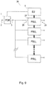
- a schematic block diagram of a power converter system 26 is disclosed.
- the power converter system 26 comprises a PCM 1, at least one power supply unit (PSU) 27, and an EU 9.
- the PSU 27 is in one embodiment a converter of "buck" type.
- the PSU 27 having an input side 28 and an output side 29.
- the input side 28 of the PSU 27 is operatively connected to the output terminal 3 of the PCM 1, and the output side 29 of the at least one PSU 27 is arranged to provide a load with output voltage from the PSU 27.
- Said EU 9 is operable for controlling the output voltage from the PCM 1 as well as monitoring the PCM 1 and the at least one PSU 27.
- the at least one PSU 27 arranged to provide a different output voltage based on signals received from the load.
- loads can for example be a central processing unit that needs different supply voltages based on the operating mode thereof.
- the power converter system 26 disclosed herein is advantageously used in connection with adaptive bus voltage.
- This adaptive bus voltage involves measuring the actual load and based on that measurement adapt the bus voltage at the output terminal 3 of the PCM 1 in order to provide optimum conditions for the PSU 27.
- a power converter system 26 is the range of adaptive output voltages from the PCM 1 adjusted by means of programming the PCM 1 during manufacturing and the EU 9 is only operatively connected during programming.
- a schematic block diagram of a power converter system 30 is disclosed.
- the power converter system 30 comprises a PCM 1, at least one power supply unit (PSU) 27.
- the PSU 27 having an input side 28 and an output side 29.
- the input side 28 of the PSU 27 is operatively connected to the output terminal 3 of the PCM 1, and the output side 29 of the at least one PSU 27 is arranged to provide a load with output voltage from the PSU 27.
- peak output mode be of great importance for adaptive control thereof. This is due to the fact that the recording in computer readable memory of utilization of peak output mode can be used in a feedback loop provided for adaptive optimization of the output voltage at the output terminal 3 of the PCM 1. This adaptive optimization can be performed either automatically or manually by an operator.
Landscapes
- Engineering & Computer Science (AREA)
- Power Engineering (AREA)
- Dc-Dc Converters (AREA)
- Inverter Devices (AREA)
Applications Claiming Priority (1)
| Application Number | Priority Date | Filing Date | Title |
|---|---|---|---|
| PCT/SE2011/051492 WO2013085442A1 (en) | 2011-12-09 | 2011-12-09 | Method for operating a power converter module and a device therefor |
Publications (2)
| Publication Number | Publication Date |
|---|---|
| EP2789084A1 EP2789084A1 (en) | 2014-10-15 |
| EP2789084B1 true EP2789084B1 (en) | 2019-02-20 |
Family
ID=45464071
Family Applications (1)
| Application Number | Title | Priority Date | Filing Date |
|---|---|---|---|
| EP11805667.0A Not-in-force EP2789084B1 (en) | 2011-12-09 | 2011-12-09 | Method for operating a power converter module and a device therefor |
Country Status (5)
| Country | Link |
|---|---|
| US (1) | US9515543B2 (enExample) |
| EP (1) | EP2789084B1 (enExample) |
| CN (1) | CN103959621B (enExample) |
| IN (1) | IN2014DN03188A (enExample) |
| WO (1) | WO2013085442A1 (enExample) |
Cited By (1)
| Publication number | Priority date | Publication date | Assignee | Title |
|---|---|---|---|---|
| KR20190020150A (ko) * | 2017-07-31 | 2019-02-27 | 주식회사 엘지화학 | Dc-dc 전압 컨버터를 벅 동작 모드에서 안전 동작 모드로 전환하는 제어 시스템 |
Families Citing this family (3)
| Publication number | Priority date | Publication date | Assignee | Title |
|---|---|---|---|---|
| US9729077B2 (en) * | 2015-01-16 | 2017-08-08 | Graco Minnesota Inc. | Front end protection power controller |
| TWI774126B (zh) * | 2020-11-18 | 2022-08-11 | 久元電子股份有限公司 | 電源調整電路、可調式電源供應系統及其方法 |
| CN116661543B (zh) * | 2023-07-28 | 2023-10-20 | 常州满旺半导体科技有限公司 | 一种基于低功耗电压源的智能化调节系统及方法 |
Family Cites Families (8)
| Publication number | Priority date | Publication date | Assignee | Title |
|---|---|---|---|---|
| IT1110628B (it) * | 1979-01-30 | 1985-12-23 | Sp El Srl | Circuito per la protezione automatica dei transistori di potenza particolarmente per convertitori a commutazione o simili |
| AT412693B (de) * | 2002-09-20 | 2005-05-25 | Siemens Ag Oesterreich | Verfahren zum steuern des abschaltens bei überlastzuständen eines schaltnetzteils |
| US20060061922A1 (en) * | 2004-09-22 | 2006-03-23 | Cellex Power Products, Inc. | Hybrid power supply system having energy storage device protection circuit |
| US7239119B2 (en) * | 2004-11-05 | 2007-07-03 | Power Integrations, Inc. | Method and apparatus to provide temporary peak power from a switching regulator |
| DE102005043882B4 (de) * | 2005-09-14 | 2014-05-28 | Siemens Aktiengesellschaft | Verfahren zum Betreiben von Schaltnetzteilen |
| DE102010001817A1 (de) * | 2010-02-11 | 2011-08-11 | Robert Bosch GmbH, 70469 | Regelungskonzept mit Grenzwertmanagement für DC/DC-Wandler in einem Energiesystem |
| JP2011193054A (ja) * | 2010-03-11 | 2011-09-29 | Fujitsu Ltd | 電源装置及び電源装置制御方法 |
| TWI458228B (zh) * | 2011-10-26 | 2014-10-21 | Acbel Polytech Inc | Soft start control method and device for power supply |
-
2011
- 2011-12-09 IN IN3188DEN2014 patent/IN2014DN03188A/en unknown
- 2011-12-09 EP EP11805667.0A patent/EP2789084B1/en not_active Not-in-force
- 2011-12-09 WO PCT/SE2011/051492 patent/WO2013085442A1/en not_active Ceased
- 2011-12-09 US US14/357,715 patent/US9515543B2/en not_active Expired - Fee Related
- 2011-12-09 CN CN201180075392.2A patent/CN103959621B/zh not_active Expired - Fee Related
Non-Patent Citations (1)
| Title |
|---|
| None * |
Cited By (1)
| Publication number | Priority date | Publication date | Assignee | Title |
|---|---|---|---|---|
| KR20190020150A (ko) * | 2017-07-31 | 2019-02-27 | 주식회사 엘지화학 | Dc-dc 전압 컨버터를 벅 동작 모드에서 안전 동작 모드로 전환하는 제어 시스템 |
Also Published As
| Publication number | Publication date |
|---|---|
| EP2789084A1 (en) | 2014-10-15 |
| IN2014DN03188A (enExample) | 2015-05-22 |
| WO2013085442A1 (en) | 2013-06-13 |
| CN103959621A (zh) | 2014-07-30 |
| US20140327414A1 (en) | 2014-11-06 |
| CN103959621B (zh) | 2017-09-12 |
| US9515543B2 (en) | 2016-12-06 |
Similar Documents
| Publication | Publication Date | Title |
|---|---|---|
| EP3305022B1 (en) | Led driver and driving method | |
| US20230198261A1 (en) | Power supply system including dc-to-dc converter and control method therefor | |
| US7439720B2 (en) | Constant-peak-current minimum-off-time pulse frequency modulator for switching regulators | |
| US8963425B2 (en) | Power supply device, lamp fitting, and vehicle | |
| EP3244524B1 (en) | Power converter and control method thereof | |
| US7586296B2 (en) | Power supply apparatus | |
| JP5388640B2 (ja) | キャパシタモジュールの均等化制御回路及び均等化制御回路を備えた均等化制御装置 | |
| CA3008730A1 (en) | Emergency lighting system | |
| US20120297104A1 (en) | Controlled intermediate bus architecture optimization | |
| US11271483B2 (en) | Bias power regulator circuit for isolated converters with a wide output voltage range | |
| KR20120066603A (ko) | Dc/dc 컨버터와 그것을 이용한 전원 장치 및 전자 기기 | |
| EP3192327B1 (en) | Led dimmer circuit and method | |
| CN101483383A (zh) | 用于功率转换器的具有可编程反馈电路的切换控制器 | |
| EP2789084B1 (en) | Method for operating a power converter module and a device therefor | |
| CN111106601B (zh) | 直流电压分布系统的控制 | |
| US8710803B2 (en) | Charging current control method and charging system | |
| US7898218B2 (en) | Power supply topologies with PWM frequency control | |
| US11496052B2 (en) | Insulated power supply circuit | |
| JP4321467B2 (ja) | パワースイッチング装置 | |
| JP4379396B2 (ja) | 昇降圧チョッパ式dc−dcコンバータ | |
| US10637359B2 (en) | Power converter controller, power converter, and corresponding methods | |
| WO2012032621A1 (ja) | キャパシタを用いた蓄電装置、その充電制御装置、および、その充電制御方法 | |
| JP2012135116A (ja) | スイッチング電源装置 | |
| JP2019068526A (ja) | コンバータシステム | |
| KR20110072013A (ko) | 양방향 컨버터 제어 방법 |
Legal Events
| Date | Code | Title | Description |
|---|---|---|---|
| PUAI | Public reference made under article 153(3) epc to a published international application that has entered the european phase |
Free format text: ORIGINAL CODE: 0009012 |
|
| 17P | Request for examination filed |
Effective date: 20140702 |
|
| AK | Designated contracting states |
Kind code of ref document: A1 Designated state(s): AL AT BE BG CH CY CZ DE DK EE ES FI FR GB GR HR HU IE IS IT LI LT LU LV MC MK MT NL NO PL PT RO RS SE SI SK SM TR |
|
| DAX | Request for extension of the european patent (deleted) | ||
| STAA | Information on the status of an ep patent application or granted ep patent |
Free format text: STATUS: EXAMINATION IS IN PROGRESS |
|
| 17Q | First examination report despatched |
Effective date: 20170217 |
|
| GRAP | Despatch of communication of intention to grant a patent |
Free format text: ORIGINAL CODE: EPIDOSNIGR1 |
|
| STAA | Information on the status of an ep patent application or granted ep patent |
Free format text: STATUS: GRANT OF PATENT IS INTENDED |
|
| RIC1 | Information provided on ipc code assigned before grant |
Ipc: G05F 1/56 20060101ALI20180919BHEP Ipc: H02M 1/00 20060101ALI20180919BHEP Ipc: H02M 1/32 20070101AFI20180919BHEP |
|
| INTG | Intention to grant announced |
Effective date: 20181018 |
|
| GRAS | Grant fee paid |
Free format text: ORIGINAL CODE: EPIDOSNIGR3 |
|
| GRAA | (expected) grant |
Free format text: ORIGINAL CODE: 0009210 |
|
| STAA | Information on the status of an ep patent application or granted ep patent |
Free format text: STATUS: THE PATENT HAS BEEN GRANTED |
|
| AK | Designated contracting states |
Kind code of ref document: B1 Designated state(s): AL AT BE BG CH CY CZ DE DK EE ES FI FR GB GR HR HU IE IS IT LI LT LU LV MC MK MT NL NO PL PT RO RS SE SI SK SM TR |
|
| REG | Reference to a national code |
Ref country code: GB Ref legal event code: FG4D |
|
| REG | Reference to a national code |
Ref country code: CH Ref legal event code: EP |
|
| REG | Reference to a national code |
Ref country code: DE Ref legal event code: R096 Ref document number: 602011056401 Country of ref document: DE |
|
| REG | Reference to a national code |
Ref country code: AT Ref legal event code: REF Ref document number: 1099478 Country of ref document: AT Kind code of ref document: T Effective date: 20190315 |
|
| REG | Reference to a national code |
Ref country code: IE Ref legal event code: FG4D |
|
| REG | Reference to a national code |
Ref country code: NL Ref legal event code: FP |
|
| REG | Reference to a national code |
Ref country code: LT Ref legal event code: MG4D |
|
| PG25 | Lapsed in a contracting state [announced via postgrant information from national office to epo] |
Ref country code: FI Free format text: LAPSE BECAUSE OF FAILURE TO SUBMIT A TRANSLATION OF THE DESCRIPTION OR TO PAY THE FEE WITHIN THE PRESCRIBED TIME-LIMIT Effective date: 20190220 Ref country code: SE Free format text: LAPSE BECAUSE OF FAILURE TO SUBMIT A TRANSLATION OF THE DESCRIPTION OR TO PAY THE FEE WITHIN THE PRESCRIBED TIME-LIMIT Effective date: 20190220 Ref country code: PT Free format text: LAPSE BECAUSE OF FAILURE TO SUBMIT A TRANSLATION OF THE DESCRIPTION OR TO PAY THE FEE WITHIN THE PRESCRIBED TIME-LIMIT Effective date: 20190620 Ref country code: NO Free format text: LAPSE BECAUSE OF FAILURE TO SUBMIT A TRANSLATION OF THE DESCRIPTION OR TO PAY THE FEE WITHIN THE PRESCRIBED TIME-LIMIT Effective date: 20190520 Ref country code: LT Free format text: LAPSE BECAUSE OF FAILURE TO SUBMIT A TRANSLATION OF THE DESCRIPTION OR TO PAY THE FEE WITHIN THE PRESCRIBED TIME-LIMIT Effective date: 20190220 |
|
| PG25 | Lapsed in a contracting state [announced via postgrant information from national office to epo] |
Ref country code: LV Free format text: LAPSE BECAUSE OF FAILURE TO SUBMIT A TRANSLATION OF THE DESCRIPTION OR TO PAY THE FEE WITHIN THE PRESCRIBED TIME-LIMIT Effective date: 20190220 Ref country code: RS Free format text: LAPSE BECAUSE OF FAILURE TO SUBMIT A TRANSLATION OF THE DESCRIPTION OR TO PAY THE FEE WITHIN THE PRESCRIBED TIME-LIMIT Effective date: 20190220 Ref country code: HR Free format text: LAPSE BECAUSE OF FAILURE TO SUBMIT A TRANSLATION OF THE DESCRIPTION OR TO PAY THE FEE WITHIN THE PRESCRIBED TIME-LIMIT Effective date: 20190220 Ref country code: IS Free format text: LAPSE BECAUSE OF FAILURE TO SUBMIT A TRANSLATION OF THE DESCRIPTION OR TO PAY THE FEE WITHIN THE PRESCRIBED TIME-LIMIT Effective date: 20190620 Ref country code: BG Free format text: LAPSE BECAUSE OF FAILURE TO SUBMIT A TRANSLATION OF THE DESCRIPTION OR TO PAY THE FEE WITHIN THE PRESCRIBED TIME-LIMIT Effective date: 20190520 Ref country code: GR Free format text: LAPSE BECAUSE OF FAILURE TO SUBMIT A TRANSLATION OF THE DESCRIPTION OR TO PAY THE FEE WITHIN THE PRESCRIBED TIME-LIMIT Effective date: 20190521 |
|
| REG | Reference to a national code |
Ref country code: AT Ref legal event code: MK05 Ref document number: 1099478 Country of ref document: AT Kind code of ref document: T Effective date: 20190220 |
|
| PG25 | Lapsed in a contracting state [announced via postgrant information from national office to epo] |
Ref country code: EE Free format text: LAPSE BECAUSE OF FAILURE TO SUBMIT A TRANSLATION OF THE DESCRIPTION OR TO PAY THE FEE WITHIN THE PRESCRIBED TIME-LIMIT Effective date: 20190220 Ref country code: IT Free format text: LAPSE BECAUSE OF FAILURE TO SUBMIT A TRANSLATION OF THE DESCRIPTION OR TO PAY THE FEE WITHIN THE PRESCRIBED TIME-LIMIT Effective date: 20190220 Ref country code: DK Free format text: LAPSE BECAUSE OF FAILURE TO SUBMIT A TRANSLATION OF THE DESCRIPTION OR TO PAY THE FEE WITHIN THE PRESCRIBED TIME-LIMIT Effective date: 20190220 Ref country code: CZ Free format text: LAPSE BECAUSE OF FAILURE TO SUBMIT A TRANSLATION OF THE DESCRIPTION OR TO PAY THE FEE WITHIN THE PRESCRIBED TIME-LIMIT Effective date: 20190220 Ref country code: RO Free format text: LAPSE BECAUSE OF FAILURE TO SUBMIT A TRANSLATION OF THE DESCRIPTION OR TO PAY THE FEE WITHIN THE PRESCRIBED TIME-LIMIT Effective date: 20190220 Ref country code: SK Free format text: LAPSE BECAUSE OF FAILURE TO SUBMIT A TRANSLATION OF THE DESCRIPTION OR TO PAY THE FEE WITHIN THE PRESCRIBED TIME-LIMIT Effective date: 20190220 Ref country code: AL Free format text: LAPSE BECAUSE OF FAILURE TO SUBMIT A TRANSLATION OF THE DESCRIPTION OR TO PAY THE FEE WITHIN THE PRESCRIBED TIME-LIMIT Effective date: 20190220 Ref country code: ES Free format text: LAPSE BECAUSE OF FAILURE TO SUBMIT A TRANSLATION OF THE DESCRIPTION OR TO PAY THE FEE WITHIN THE PRESCRIBED TIME-LIMIT Effective date: 20190220 |
|
| REG | Reference to a national code |
Ref country code: DE Ref legal event code: R097 Ref document number: 602011056401 Country of ref document: DE |
|
| PG25 | Lapsed in a contracting state [announced via postgrant information from national office to epo] |
Ref country code: SM Free format text: LAPSE BECAUSE OF FAILURE TO SUBMIT A TRANSLATION OF THE DESCRIPTION OR TO PAY THE FEE WITHIN THE PRESCRIBED TIME-LIMIT Effective date: 20190220 Ref country code: PL Free format text: LAPSE BECAUSE OF FAILURE TO SUBMIT A TRANSLATION OF THE DESCRIPTION OR TO PAY THE FEE WITHIN THE PRESCRIBED TIME-LIMIT Effective date: 20190220 |
|
| PLBE | No opposition filed within time limit |
Free format text: ORIGINAL CODE: 0009261 |
|
| STAA | Information on the status of an ep patent application or granted ep patent |
Free format text: STATUS: NO OPPOSITION FILED WITHIN TIME LIMIT |
|
| PG25 | Lapsed in a contracting state [announced via postgrant information from national office to epo] |
Ref country code: AT Free format text: LAPSE BECAUSE OF FAILURE TO SUBMIT A TRANSLATION OF THE DESCRIPTION OR TO PAY THE FEE WITHIN THE PRESCRIBED TIME-LIMIT Effective date: 20190220 |
|
| 26N | No opposition filed |
Effective date: 20191121 |
|
| PG25 | Lapsed in a contracting state [announced via postgrant information from national office to epo] |
Ref country code: SI Free format text: LAPSE BECAUSE OF FAILURE TO SUBMIT A TRANSLATION OF THE DESCRIPTION OR TO PAY THE FEE WITHIN THE PRESCRIBED TIME-LIMIT Effective date: 20190220 |
|
| PG25 | Lapsed in a contracting state [announced via postgrant information from national office to epo] |
Ref country code: TR Free format text: LAPSE BECAUSE OF FAILURE TO SUBMIT A TRANSLATION OF THE DESCRIPTION OR TO PAY THE FEE WITHIN THE PRESCRIBED TIME-LIMIT Effective date: 20190220 |
|
| REG | Reference to a national code |
Ref country code: DE Ref legal event code: R119 Ref document number: 602011056401 Country of ref document: DE |
|
| REG | Reference to a national code |
Ref country code: CH Ref legal event code: PL |
|
| REG | Reference to a national code |
Ref country code: NL Ref legal event code: MM Effective date: 20200101 |
|
| REG | Reference to a national code |
Ref country code: BE Ref legal event code: MM Effective date: 20191231 |
|
| PG25 | Lapsed in a contracting state [announced via postgrant information from national office to epo] |
Ref country code: MC Free format text: LAPSE BECAUSE OF FAILURE TO SUBMIT A TRANSLATION OF THE DESCRIPTION OR TO PAY THE FEE WITHIN THE PRESCRIBED TIME-LIMIT Effective date: 20190220 |
|
| GBPC | Gb: european patent ceased through non-payment of renewal fee |
Effective date: 20191209 |
|
| PG25 | Lapsed in a contracting state [announced via postgrant information from national office to epo] |
Ref country code: NL Free format text: LAPSE BECAUSE OF NON-PAYMENT OF DUE FEES Effective date: 20200101 |
|
| PG25 | Lapsed in a contracting state [announced via postgrant information from national office to epo] |
Ref country code: LU Free format text: LAPSE BECAUSE OF NON-PAYMENT OF DUE FEES Effective date: 20191209 Ref country code: DE Free format text: LAPSE BECAUSE OF NON-PAYMENT OF DUE FEES Effective date: 20200701 Ref country code: GB Free format text: LAPSE BECAUSE OF NON-PAYMENT OF DUE FEES Effective date: 20191209 Ref country code: IE Free format text: LAPSE BECAUSE OF NON-PAYMENT OF DUE FEES Effective date: 20191209 Ref country code: FR Free format text: LAPSE BECAUSE OF NON-PAYMENT OF DUE FEES Effective date: 20191231 |
|
| PG25 | Lapsed in a contracting state [announced via postgrant information from national office to epo] |
Ref country code: CH Free format text: LAPSE BECAUSE OF NON-PAYMENT OF DUE FEES Effective date: 20191231 Ref country code: LI Free format text: LAPSE BECAUSE OF NON-PAYMENT OF DUE FEES Effective date: 20191231 Ref country code: BE Free format text: LAPSE BECAUSE OF NON-PAYMENT OF DUE FEES Effective date: 20191231 |
|
| PG25 | Lapsed in a contracting state [announced via postgrant information from national office to epo] |
Ref country code: CY Free format text: LAPSE BECAUSE OF FAILURE TO SUBMIT A TRANSLATION OF THE DESCRIPTION OR TO PAY THE FEE WITHIN THE PRESCRIBED TIME-LIMIT Effective date: 20190220 |
|
| PG25 | Lapsed in a contracting state [announced via postgrant information from national office to epo] |
Ref country code: HU Free format text: LAPSE BECAUSE OF FAILURE TO SUBMIT A TRANSLATION OF THE DESCRIPTION OR TO PAY THE FEE WITHIN THE PRESCRIBED TIME-LIMIT; INVALID AB INITIO Effective date: 20111209 Ref country code: MT Free format text: LAPSE BECAUSE OF FAILURE TO SUBMIT A TRANSLATION OF THE DESCRIPTION OR TO PAY THE FEE WITHIN THE PRESCRIBED TIME-LIMIT Effective date: 20190220 |
|
| PG25 | Lapsed in a contracting state [announced via postgrant information from national office to epo] |
Ref country code: MK Free format text: LAPSE BECAUSE OF FAILURE TO SUBMIT A TRANSLATION OF THE DESCRIPTION OR TO PAY THE FEE WITHIN THE PRESCRIBED TIME-LIMIT Effective date: 20190220 |