EP2782119A1 - Procédé de modification localisée des contraintes dans un substrat du type SOI, en particulier FD SOI, et dispositif correspondant - Google Patents
Procédé de modification localisée des contraintes dans un substrat du type SOI, en particulier FD SOI, et dispositif correspondant Download PDFInfo
- Publication number
- EP2782119A1 EP2782119A1 EP14160802.6A EP14160802A EP2782119A1 EP 2782119 A1 EP2782119 A1 EP 2782119A1 EP 14160802 A EP14160802 A EP 14160802A EP 2782119 A1 EP2782119 A1 EP 2782119A1
- Authority
- EP
- European Patent Office
- Prior art keywords
- silicon
- film
- constrained
- substrate
- zone
- Prior art date
- Legal status (The legal status is an assumption and is not a legal conclusion. Google has not performed a legal analysis and makes no representation as to the accuracy of the status listed.)
- Granted
Links
Images


Classifications
-
- H—ELECTRICITY
- H10—SEMICONDUCTOR DEVICES; ELECTRIC SOLID-STATE DEVICES NOT OTHERWISE PROVIDED FOR
- H10D—INORGANIC ELECTRIC SEMICONDUCTOR DEVICES
- H10D30/00—Field-effect transistors [FET]
- H10D30/60—Insulated-gate field-effect transistors [IGFET]
- H10D30/791—Arrangements for exerting mechanical stress on the crystal lattice of the channel regions
- H10D30/796—Arrangements for exerting mechanical stress on the crystal lattice of the channel regions having memorised stress for introducing strain in the channel regions, e.g. recrystallised polysilicon gates
-
- H—ELECTRICITY
- H10—SEMICONDUCTOR DEVICES; ELECTRIC SOLID-STATE DEVICES NOT OTHERWISE PROVIDED FOR
- H10D—INORGANIC ELECTRIC SEMICONDUCTOR DEVICES
- H10D30/00—Field-effect transistors [FET]
- H10D30/60—Insulated-gate field-effect transistors [IGFET]
- H10D30/637—Lateral IGFETs having no inversion channels, e.g. buried channel lateral IGFETs, normally-on lateral IGFETs or depletion-mode lateral IGFETs
-
- H—ELECTRICITY
- H10—SEMICONDUCTOR DEVICES; ELECTRIC SOLID-STATE DEVICES NOT OTHERWISE PROVIDED FOR
- H10D—INORGANIC ELECTRIC SEMICONDUCTOR DEVICES
- H10D62/00—Semiconductor bodies, or regions thereof, of devices having potential barriers
- H10D62/10—Shapes, relative sizes or dispositions of the regions of the semiconductor bodies; Shapes of the semiconductor bodies
- H10D62/102—Constructional design considerations for preventing surface leakage or controlling electric field concentration
- H10D62/103—Constructional design considerations for preventing surface leakage or controlling electric field concentration for increasing or controlling the breakdown voltage of reverse-biased devices
-
- H—ELECTRICITY
- H10—SEMICONDUCTOR DEVICES; ELECTRIC SOLID-STATE DEVICES NOT OTHERWISE PROVIDED FOR
- H10D—INORGANIC ELECTRIC SEMICONDUCTOR DEVICES
- H10D62/00—Semiconductor bodies, or regions thereof, of devices having potential barriers
- H10D62/10—Shapes, relative sizes or dispositions of the regions of the semiconductor bodies; Shapes of the semiconductor bodies
- H10D62/113—Isolations within a component, i.e. internal isolations
-
- H—ELECTRICITY
- H10—SEMICONDUCTOR DEVICES; ELECTRIC SOLID-STATE DEVICES NOT OTHERWISE PROVIDED FOR
- H10D—INORGANIC ELECTRIC SEMICONDUCTOR DEVICES
- H10D62/00—Semiconductor bodies, or regions thereof, of devices having potential barriers
- H10D62/80—Semiconductor bodies, or regions thereof, of devices having potential barriers characterised by the materials
- H10D62/83—Semiconductor bodies, or regions thereof, of devices having potential barriers characterised by the materials being Group IV materials, e.g. B-doped Si or undoped Ge
-
- H—ELECTRICITY
- H10—SEMICONDUCTOR DEVICES; ELECTRIC SOLID-STATE DEVICES NOT OTHERWISE PROVIDED FOR
- H10D—INORGANIC ELECTRIC SEMICONDUCTOR DEVICES
- H10D62/00—Semiconductor bodies, or regions thereof, of devices having potential barriers
- H10D62/80—Semiconductor bodies, or regions thereof, of devices having potential barriers characterised by the materials
- H10D62/83—Semiconductor bodies, or regions thereof, of devices having potential barriers characterised by the materials being Group IV materials, e.g. B-doped Si or undoped Ge
- H10D62/832—Semiconductor bodies, or regions thereof, of devices having potential barriers characterised by the materials being Group IV materials, e.g. B-doped Si or undoped Ge being Group IV materials comprising two or more elements, e.g. SiGe
-
- H—ELECTRICITY
- H10—SEMICONDUCTOR DEVICES; ELECTRIC SOLID-STATE DEVICES NOT OTHERWISE PROVIDED FOR
- H10D—INORGANIC ELECTRIC SEMICONDUCTOR DEVICES
- H10D84/00—Integrated devices formed in or on semiconductor substrates that comprise only semiconducting layers, e.g. on Si wafers or on GaAs-on-Si wafers
- H10D84/01—Manufacture or treatment
- H10D84/0123—Integrating together multiple components covered by H10D12/00 or H10D30/00, e.g. integrating multiple IGBTs
- H10D84/0126—Integrating together multiple components covered by H10D12/00 or H10D30/00, e.g. integrating multiple IGBTs the components including insulated gates, e.g. IGFETs
- H10D84/0165—Integrating together multiple components covered by H10D12/00 or H10D30/00, e.g. integrating multiple IGBTs the components including insulated gates, e.g. IGFETs the components including complementary IGFETs, e.g. CMOS devices
- H10D84/0167—Manufacturing their channels
-
- H—ELECTRICITY
- H10—SEMICONDUCTOR DEVICES; ELECTRIC SOLID-STATE DEVICES NOT OTHERWISE PROVIDED FOR
- H10D—INORGANIC ELECTRIC SEMICONDUCTOR DEVICES
- H10D84/00—Integrated devices formed in or on semiconductor substrates that comprise only semiconducting layers, e.g. on Si wafers or on GaAs-on-Si wafers
- H10D84/01—Manufacture or treatment
- H10D84/02—Manufacture or treatment characterised by using material-based technologies
- H10D84/03—Manufacture or treatment characterised by using material-based technologies using Group IV technology, e.g. silicon technology or silicon-carbide [SiC] technology
- H10D84/038—Manufacture or treatment characterised by using material-based technologies using Group IV technology, e.g. silicon technology or silicon-carbide [SiC] technology using silicon technology, e.g. SiGe
-
- H—ELECTRICITY
- H10—SEMICONDUCTOR DEVICES; ELECTRIC SOLID-STATE DEVICES NOT OTHERWISE PROVIDED FOR
- H10D—INORGANIC ELECTRIC SEMICONDUCTOR DEVICES
- H10D84/00—Integrated devices formed in or on semiconductor substrates that comprise only semiconducting layers, e.g. on Si wafers or on GaAs-on-Si wafers
- H10D84/80—Integrated devices formed in or on semiconductor substrates that comprise only semiconducting layers, e.g. on Si wafers or on GaAs-on-Si wafers characterised by the integration of at least one component covered by groups H10D12/00 or H10D30/00, e.g. integration of IGFETs
- H10D84/82—Integrated devices formed in or on semiconductor substrates that comprise only semiconducting layers, e.g. on Si wafers or on GaAs-on-Si wafers characterised by the integration of at least one component covered by groups H10D12/00 or H10D30/00, e.g. integration of IGFETs of only field-effect components
- H10D84/83—Integrated devices formed in or on semiconductor substrates that comprise only semiconducting layers, e.g. on Si wafers or on GaAs-on-Si wafers characterised by the integration of at least one component covered by groups H10D12/00 or H10D30/00, e.g. integration of IGFETs of only field-effect components of only insulated-gate FETs [IGFET]
- H10D84/85—Complementary IGFETs, e.g. CMOS
-
- H—ELECTRICITY
- H10—SEMICONDUCTOR DEVICES; ELECTRIC SOLID-STATE DEVICES NOT OTHERWISE PROVIDED FOR
- H10D—INORGANIC ELECTRIC SEMICONDUCTOR DEVICES
- H10D86/00—Integrated devices formed in or on insulating or conducting substrates, e.g. formed in silicon-on-insulator [SOI] substrates or on stainless steel or glass substrates
-
- H—ELECTRICITY
- H10—SEMICONDUCTOR DEVICES; ELECTRIC SOLID-STATE DEVICES NOT OTHERWISE PROVIDED FOR
- H10D—INORGANIC ELECTRIC SEMICONDUCTOR DEVICES
- H10D86/00—Integrated devices formed in or on insulating or conducting substrates, e.g. formed in silicon-on-insulator [SOI] substrates or on stainless steel or glass substrates
- H10D86/01—Manufacture or treatment
-
- H—ELECTRICITY
- H10—SEMICONDUCTOR DEVICES; ELECTRIC SOLID-STATE DEVICES NOT OTHERWISE PROVIDED FOR
- H10D—INORGANIC ELECTRIC SEMICONDUCTOR DEVICES
- H10D86/00—Integrated devices formed in or on insulating or conducting substrates, e.g. formed in silicon-on-insulator [SOI] substrates or on stainless steel or glass substrates
- H10D86/201—Integrated devices formed in or on insulating or conducting substrates, e.g. formed in silicon-on-insulator [SOI] substrates or on stainless steel or glass substrates the substrates comprising an insulating layer on a semiconductor body, e.g. SOI
-
- H—ELECTRICITY
- H10—SEMICONDUCTOR DEVICES; ELECTRIC SOLID-STATE DEVICES NOT OTHERWISE PROVIDED FOR
- H10P—GENERIC PROCESSES OR APPARATUS FOR THE MANUFACTURE OR TREATMENT OF DEVICES COVERED BY CLASS H10
- H10P14/00—Formation of materials, e.g. in the shape of layers or pillars
- H10P14/20—Formation of materials, e.g. in the shape of layers or pillars of semiconductor materials
- H10P14/27—Formation of materials, e.g. in the shape of layers or pillars of semiconductor materials using selective deposition, e.g. simultaneous growth of monocrystalline and non-monocrystalline semiconductor materials
- H10P14/271—Formation of materials, e.g. in the shape of layers or pillars of semiconductor materials using selective deposition, e.g. simultaneous growth of monocrystalline and non-monocrystalline semiconductor materials characterised by the preparation of substrate for selective deposition
-
- H—ELECTRICITY
- H10—SEMICONDUCTOR DEVICES; ELECTRIC SOLID-STATE DEVICES NOT OTHERWISE PROVIDED FOR
- H10P—GENERIC PROCESSES OR APPARATUS FOR THE MANUFACTURE OR TREATMENT OF DEVICES COVERED BY CLASS H10
- H10P14/00—Formation of materials, e.g. in the shape of layers or pillars
- H10P14/20—Formation of materials, e.g. in the shape of layers or pillars of semiconductor materials
- H10P14/29—Formation of materials, e.g. in the shape of layers or pillars of semiconductor materials characterised by the substrates
- H10P14/2901—Materials
- H10P14/2902—Materials being Group IVA materials
- H10P14/2905—Silicon, silicon germanium or germanium
-
- H—ELECTRICITY
- H10—SEMICONDUCTOR DEVICES; ELECTRIC SOLID-STATE DEVICES NOT OTHERWISE PROVIDED FOR
- H10P—GENERIC PROCESSES OR APPARATUS FOR THE MANUFACTURE OR TREATMENT OF DEVICES COVERED BY CLASS H10
- H10P14/00—Formation of materials, e.g. in the shape of layers or pillars
- H10P14/20—Formation of materials, e.g. in the shape of layers or pillars of semiconductor materials
- H10P14/29—Formation of materials, e.g. in the shape of layers or pillars of semiconductor materials characterised by the substrates
- H10P14/2901—Materials
- H10P14/2922—Materials being non-crystalline insulating materials, e.g. glass or polymers
-
- H—ELECTRICITY
- H10—SEMICONDUCTOR DEVICES; ELECTRIC SOLID-STATE DEVICES NOT OTHERWISE PROVIDED FOR
- H10P—GENERIC PROCESSES OR APPARATUS FOR THE MANUFACTURE OR TREATMENT OF DEVICES COVERED BY CLASS H10
- H10P14/00—Formation of materials, e.g. in the shape of layers or pillars
- H10P14/20—Formation of materials, e.g. in the shape of layers or pillars of semiconductor materials
- H10P14/34—Deposited materials, e.g. layers
- H10P14/3402—Deposited materials, e.g. layers characterised by the chemical composition
- H10P14/3404—Deposited materials, e.g. layers characterised by the chemical composition being Group IVA materials
- H10P14/3411—Silicon, silicon germanium or germanium
-
- H—ELECTRICITY
- H10—SEMICONDUCTOR DEVICES; ELECTRIC SOLID-STATE DEVICES NOT OTHERWISE PROVIDED FOR
- H10P—GENERIC PROCESSES OR APPARATUS FOR THE MANUFACTURE OR TREATMENT OF DEVICES COVERED BY CLASS H10
- H10P14/00—Formation of materials, e.g. in the shape of layers or pillars
- H10P14/20—Formation of materials, e.g. in the shape of layers or pillars of semiconductor materials
- H10P14/38—Formation of materials, e.g. in the shape of layers or pillars of semiconductor materials characterised by treatments done after the formation of the materials
- H10P14/3802—Crystallisation or recrystallisation of non-monocrystalline semiconductor materials, e.g. regrowth
-
- H—ELECTRICITY
- H10—SEMICONDUCTOR DEVICES; ELECTRIC SOLID-STATE DEVICES NOT OTHERWISE PROVIDED FOR
- H10P—GENERIC PROCESSES OR APPARATUS FOR THE MANUFACTURE OR TREATMENT OF DEVICES COVERED BY CLASS H10
- H10P90/00—Preparation of wafers not covered by a single main group of this subclass, e.g. wafer reinforcement
- H10P90/19—Preparing inhomogeneous wafers
- H10P90/1904—Preparing vertically inhomogeneous wafers
- H10P90/1906—Preparing SOI wafers
-
- H—ELECTRICITY
- H10—SEMICONDUCTOR DEVICES; ELECTRIC SOLID-STATE DEVICES NOT OTHERWISE PROVIDED FOR
- H10W—GENERIC PACKAGES, INTERCONNECTIONS, CONNECTORS OR OTHER CONSTRUCTIONAL DETAILS OF DEVICES COVERED BY CLASS H10
- H10W10/00—Isolation regions in semiconductor bodies between components of integrated devices
- H10W10/01—Manufacture or treatment
- H10W10/011—Manufacture or treatment of isolation regions comprising dielectric materials
- H10W10/014—Manufacture or treatment of isolation regions comprising dielectric materials using trench refilling with dielectric materials, e.g. shallow trench isolations
-
- H—ELECTRICITY
- H10—SEMICONDUCTOR DEVICES; ELECTRIC SOLID-STATE DEVICES NOT OTHERWISE PROVIDED FOR
- H10W—GENERIC PACKAGES, INTERCONNECTIONS, CONNECTORS OR OTHER CONSTRUCTIONAL DETAILS OF DEVICES COVERED BY CLASS H10
- H10W10/00—Isolation regions in semiconductor bodies between components of integrated devices
- H10W10/01—Manufacture or treatment
- H10W10/061—Manufacture or treatment using SOI processes together with lateral isolation, e.g. combinations of SOI and shallow trench isolations
-
- H—ELECTRICITY
- H10—SEMICONDUCTOR DEVICES; ELECTRIC SOLID-STATE DEVICES NOT OTHERWISE PROVIDED FOR
- H10W—GENERIC PACKAGES, INTERCONNECTIONS, CONNECTORS OR OTHER CONSTRUCTIONAL DETAILS OF DEVICES COVERED BY CLASS H10
- H10W10/00—Isolation regions in semiconductor bodies between components of integrated devices
- H10W10/10—Isolation regions comprising dielectric materials
- H10W10/17—Isolation regions comprising dielectric materials formed using trench refilling with dielectric materials, e.g. shallow trench isolations
-
- H—ELECTRICITY
- H10—SEMICONDUCTOR DEVICES; ELECTRIC SOLID-STATE DEVICES NOT OTHERWISE PROVIDED FOR
- H10W—GENERIC PACKAGES, INTERCONNECTIONS, CONNECTORS OR OTHER CONSTRUCTIONAL DETAILS OF DEVICES COVERED BY CLASS H10
- H10W10/00—Isolation regions in semiconductor bodies between components of integrated devices
- H10W10/10—Isolation regions comprising dielectric materials
- H10W10/181—Semiconductor-on-insulator [SOI] isolation regions, e.g. buried oxide regions of SOI wafers
Definitions
- the invention relates to integrated circuits, and in particular silicon-on-insulator (SOI) substrates, more particularly completely desolated silicon-on-insulator (FD SOI) substrates, partially constrained by view of the co-integration of NMOS and PMOS transistors.
- SOI silicon-on-insulator
- FD SOI completely desolated silicon-on-insulator
- NMOS transistor When an NMOS transistor has a voltage-constrained channel, the carrier mobility increases as well as the current output, which increases its performance. On the other hand, a voltage-constrained channel degrades the performance of a PMOS transistor, in particular with regard to the mobility of the holes, which decreases.
- a method of localized modification of the stresses in a silicon-on-insulator substrate initially stressed in tension comprises an initially voltage-constrained silicon semiconductor film disposed on a so-called buried insulating layer itself disposed on an unstressed silicon support substrate;
- the process comprises forming at least one opening in the initially constrained silicon film and in the underlying buried insulating layer until reaching the unstressed silicon support substrate, a silicon epitaxy in said at least one opening from a silicon support substrate not constrained so as to fill said at least one opening, a localized amorphization of a zone of the silicon film including the said at least one epitaxial zone, a recrystallization of said at least one amorphized zone by solid phase epitaxy from the unstressed portion of silicon located in said at least one opening and in contact with the amorphized zone, in order to obtain in the silicon film constrained at least one localized region of film comprising silicon released in tension.
- the obtaining of the localized area of silicon released in tension is obtained by the combination of a localized amorphization of a zone of the silicon film and a recrystallization of this zone from a seed of silicon which lies below this amorphized zone, and more precisely in the portion of the epitaxially filled opening situated between portions of the buried insulating layer, independently of the crystallographic orientation of said silicon zone and without necessarily changing the crystallographic orientation of said zone.
- FD SOI technology offers properties of low consumption and very low voltage operation. Furthermore, in the silicon support substrate (for example a box), provision is made for the buried control electrode regions, beneath the buried insulating layer (BOX), so that the channels of the MOS transistors made in the semiconductor film. And, these buried electrode regions are polarized via contact wells connecting the boxes to the upper face of the film.
- BOX buried insulating layer
- each opening that will allow the recrystallization of the corresponding amorphized zone corresponds to a well intended to allow contact with a silicon support substrate (box for example).
- a method for producing N-channel type transistor and P-channel type transistor, for example NMOS and PMOS transistors, in a silicon-on-insulator substrate initially constrained comprising a embodiment of the P-channel transistors in said at least one localized area of voltage-released silicon obtained by the method defined above or in the compression-stressed film zone obtained by the method defined above, and an embodiment of the transistors to N channel in the film zone or zones comprising silicon forced into tension.
- a device comprising a silicon-on-insulator substrate, said substrate comprising a semiconductor film disposed on a so-called buried insulating layer itself disposed on an unstressed silicon support substrate, the semi-film conductor comprising at least a first film zone comprising voltage-constrained silicon and at least one second film zone comprising silicon released in tension, said buried insulating layer comprising at least one opening under said at least one second film zone, said opening comprising unstressed silicon.
- the substrate may advantageously be of the totally unsaturated silicon-on-insulator type.
- At least a portion of said at least one second film zone may comprise a silicon-germanium alloy so as to form a portion of film constrained in compression.
- the device may thus comprise at least one NMOS transistor formed in and on said at least one first film zone and at least one PMOS transistor formed in and on said second film zone.
- the reference DIS denotes a device, for example a semiconductor wafer having a lower region, or support substrate, 3 of unstressed silicon.
- This region 3 can be for example a box.
- This region 3 can generally comprise intrinsic silicon, that is to say undoped silicon. This being so, in practice, there is still a low level of dopants, but when this level of dopants is less than 10 15 atoms per cm3, it is nonetheless referred to as intrinsic silicon.
- This lower silicon region 3 is surmounted by a buried insulating layer 2 commonly designated by those skilled in the art under the name of "BOX" Anglo-Saxon.
- This insulating region may for example be formed of silicon dioxide.
- this buried insulating layer there is a semiconductor film 1 formed here of tension-stressed silicon. It can thus be seen here that the film 1 is part of a silicon-on-insulator substrate.
- this film 1 In FD SOI technology, the thickness of this film 1 is of the order of a few nanometers. And, it is in this film 1 that will be realized NMOS and PMOS transistors.
- a hole or an opening 4 is formed in the film 1, typically by a conventional etching operation, which extends into the buried insulating layer 2 to lead to the lower region 3 of unstressed silicon.
- the definition of the location of this zone is conventionally carried out by a mask and the amorphization comprises, in a conventional manner, a bombardment of the corresponding silicon zone by atoms, for example argon or germanium.
- the film 1 consequently comprises a localized amorphized zone 11 which is in contact with the unstressed silicon 31 resulting from the epitaxy 30 and situated between the portions of the insulating layer 2.
- the film 1 also comprises on either side of this amorphized zone 11 a film zone 10 formed of tension-stressed silicon.
- the next step ( figure 5 ) comprises a recrystallization of the amorphized zone 11 by a solid phase epitaxy 50.
- a solid phase epitaxy 50 is known to those skilled in the art under the acronym of "SPER"("Solid Phase Epitaxy Regrowth”).
- Such epitaxy is obtained from the unconstrained silicon seed 31 by heating, typically between 400 and 1000 ° C for a duration that may vary between one minute and one hour depending on the volume of the amorphized zone to be recrystallized.
- Those skilled in the art may for all practical purposes refer, with particular reference to size orders, to the recrystallization rates of the amorphized silicon in the following article: "Substrate-orientation dependence of the epitaxial regrowth rate of Si-implanted amorphous Si", L. Csepregi et al., J. Appl. Phys. 49 (7), pp 3906-3911, July 1978 .
- the film 1 comprises a localized zone 12 of film comprising silicon released in tension, and a film zone 10 comprising silicon constrained in tension.
- the constrained silicon zone 10 of the film 1 intended to receive the NMOS transistor or transistors, is masked with a resin block 6 before proceeding with the localized amorphization of the rest of the film 1.
- An amorphized zone 11 is thus obtained in contact in particular with the unstressed silicon 31.
- one or more NMOS transistors TN are formed in the film zone 10 comprising voltage-constrained silicon, the source S and drain D regions of the transistor or transistors being produced by an epitaxy followed by a dopant implantation, or by an epitaxial semiconductor (for example silicon) doped in situ (for example carbon or phosphorus).
- an epitaxial semiconductor for example silicon
- doped in situ for example carbon or phosphorus
- the PMOS transistor TP or transistors are made in the region of silicon released under voltage stress 12.
- the source S and drain D regions will be produced by dopant implantation, or by a semiconductor epitaxy (for example silicon or silicon germanium) doped in situ (for example boron).
- FIG. 13 to 16 schematically illustrate another implementation of the invention providing this time the realization of a localized area of film constrained in compression.
- a hard mask layer 90 and a resin block 91 are deposited.
- a layer 93 of a germanium silicon alloy Such a step of SiGe epitaxy is conventional and known per se. Then, a condensation step of this germanium silicon is carried out leading to a surface oxidation of the silicon germanium and to a diffusion of the germanium atoms in the underlying silicon layer 12.
- Such a conventional and known condensation step is carried out by heating the epitaxially grown silicon germanium, for example at a temperature of 900 ° C. to 1100 ° C. for a duration of the order of one second to a few minutes.
- the device DIS comprises a layer of silicon dioxide germanium constrained in compression surmounted by a layer of silicon dioxide 94 ( figure 15 ).
- a device comprising in the zone ZS1 a voltage-constrained silicon film 10 in which the NMOS transistor (s) and the constrained silicon-germanium (13) film 13 may be made. which can be achieved the PMOS transistor or transistors.
- a stress-stressed area (in compression) in one direction is constrained in compression (or in tension) in a perpendicular direction.
- An area can not be constrained in tension and compression in the same direction.
Landscapes
- Thin Film Transistor (AREA)
- Chemical & Material Sciences (AREA)
- Crystallography & Structural Chemistry (AREA)
Abstract
Description
- L'invention concerne les circuits intégrés, et notamment les substrats du type silicium sur isolant (SOI : Silicon On Insulator), plus particulièrement les substrats du type silicium sur isolant totalement désertés (FD SOI : Fully Depleted Silicon On Insulator), partiellement contraints en vue de la co-intégration de transistors NMOS et PMOS.
- Lorsqu'un transistor NMOS présente un canal contraint en tension, la mobilité des porteurs augmente de même que le courant débité ce qui augmente ses performances. Par contre, un canal contraint en tension dégrade les performances d'un transistor PMOS notamment au niveau de la mobilité des trous qui diminue.
- Il existe aujourd'hui, dans des technologies dites « substrat massif », des techniques pour contraindre en tension les canaux des transistors NMOS.
- Il existe également des substrats du type SOI dans lesquels le film de silicium, qui repose sur la couche isolante enterrée supportée par un substrat support de silicium, par exemple un caisson, est déjà contraint en tension. Mais, si cela est avantageux pour la réalisation des transistors NMOS, cela présente un inconvénient pour la réalisation des transistors PMOS.
- Selon un mode de mise en oeuvre, il est proposé de modifier de façon locale les contraintes dans un substrat du type SOI initialement contraint en tension de façon à pouvoir y réaliser des transistors PMOS, et ce d'une façon compatible avec des films minces tels que ceux utilisés dans la technologie FD SOI.
- Selon un mode de mise en oeuvre, il est également proposé de rendre contraintes en compression, les parties du film semi-conducteur dans lesquelles seront réalisés les transistors PMOS.
- Selon un mode de mise en oeuvre, il est aussi proposé de relâcher les contraintes d'une zone de silicium initialement contrainte en tension indépendamment de l'orientation cristallographique de ladite zone de silicium.
- Selon un mode de mise en oeuvre il est aussi proposé de former une zone de film semiconducteur contraient en compression de façon à améliorer les performances d'un transistor PMOS réalisé dans une telle zone de film, indépendamment de l'orientation cristallographique du film semiconducteur.
- Selon un aspect, il est proposé un procédé de modification localisé des contraintes dans un substrat du type silicium sur isolant initialement contraint en tension ; un tel substrat comprend un film semi-conducteur de silicium initialement contraint en tension disposé sur une couche isolante dite enterrée elle-même disposée sur un substrat support de silicium non contraint ;
- le procédé comprend
une formation d'au moins une ouverture dans le film de silicium initialement contraint et dans la couche isolante enterrée sous-jacente jusqu'à atteindre le substrat support de silicium non contraint,
une épitaxie de silicium dans ladite au moins une ouverture à partir substrat support de silicium non contraint de façon à combler ladite au moins une ouverture,
une amorphisation localisée d'une zone du film de silicium incluant ladite au moins une zone épitaxiée,
une recristallisation de ladite au moins une zone amorphisée par une épitaxie en phase solide à partir de la partie de silicium non contraint située dans ladite au moins une ouverture et en contact avec la zone amorphisée,
de façon à obtenir dans le film de silicium contraint au moins une zone localisée de film comportant du silicium relâché en tension. - Ainsi, selon cet aspect, l'obtention de la zone localisée de silicium relâché en tension est obtenue par la combinaison d'une amorphisation localisée d'une zone du film de silicium et d'une recristallisation de cette zone à partir d'un germe de silicium qui se situe sous cette zone amorphisée, et plus précisément dans la partie de l'ouverture comblée par épitaxie située entre des portions de la couche isolante enterrée, indépendamment de l'orientation cristallographique de ladite zone de silicium et sans forcément changer l'orientation cristallographique de ladite zone.
- Et, ceci est particulièrement intéressant pour des technologies SOI dans lesquelles le film de silicium peut être relativement fin, et tout particulièrement dans les technologies FD SOI dans lesquelles le film de silicium est particulièrement fin, typiquement de l'ordre de quelques nanomètres. En effet, dans ce cas, l'amorphisation localisée du film conduit à une amorphisation dans toute la profondeur et il est donc à ce moment-là nécessaire d'avoir sous cette zone amorphisée, un germe de silicium au contact de cette zone amorphisée pour permettre la recristallisation par épitaxie en phase solide.
- Une technologie FD SOI offre des propriétés de faible consommation et de fonctionnement à très basse tension d'alimentation. Par ailleurs, dans le substrat support de silicium (un caisson par exemple) il est prévu de disposer des régions d'électrodes de commande enterrées, sous la couche isolante enterrée (BOX) de façon à pouvoir polariser également les canaux des transistors MOS réalisés dans le film semi-conducteur. Et, ces régions d'électrodes enterrées sont polarisées par l'intermédiaire de puits de contact reliant les caissons à la face supérieure du film.
- Et, selon un mode de mise en oeuvre, chaque ouverture qui va permettre la recristallisation de la zone amorphisée correspondante, correspond à un puits destiné à permettre le contact avec substrat support de silicium (caisson par exemple).
- En d'autres termes, on peut avantageusement utiliser, pour définir des emplacements desdites ouvertures, le même masque que celui destiné à définir les emplacements de ces puits de contact. Il en résulte par conséquent une mise en oeuvre simplifiée du procédé.
- Selon un mode de mise en oeuvre, il est en outre particulièrement avantageux de former un alliage de silicium-germanium dans au moins une partie de ladite zone localisée relâchée en tension de façon à former une zone de film contraint en compression. Ceci va permettre d'améliorer encore les performances d'un transistor PMOS qui sera réalisé dans une telle zone de film comprimée.
- Selon un autre aspect, il est également proposé un procédé de réalisation de transistor du type à canal N et de transistor de type à canal P, par exemple des transistors NMOS et PMOS, dans un substrat de type silicium sur isolant initialement contraint, comprenant une réalisation des transistors à canal P dans ladite au moins une zone localisée de silicium relâchée en tension obtenue par le procédé défini ci-avant ou dans la zone de film contrainte en compression obtenue par le procédé défini ci-avant, et une réalisation des transistors à canal N dans la ou les zones de film comportant du silicium contraint en tension.
- Selon un autre aspect, il est proposé un dispositif comprenant un substrat du type silicium sur isolant, ledit substrat comportant un film semi-conducteur disposé sur une couche isolante dite enterrée elle-même disposée sur un substrat support de silicium non contraint, le film semi-conducteur comprenant au moins une première zone de film comportant du silicium contraint en tension et au moins une deuxième zone de film comportant du silicium relâché en tension, ladite couche isolante enterrée comportant au moins une ouverture sous ladite au moins une deuxième zone de film, ladite ouverture comportant du silicium non contraint.
- Le substrat peut être avantageusement du type silicium sur isolant totalement déserté.
- Par ailleurs, selon un mode de réalisation, au moins une partie de ladite au moins une deuxième zone de film peut comprendre un alliage de silicium-germanium de façon à former une partie de film contraint en compression.
- Le dispositif peut ainsi comprendre au moins un transistor NMOS réalisé dans et sur ladite au moins une première zone de film et au moins un transistor PMOS réalisé dans et sur ladite deuxième zone de film.
- D'autres avantages et caractéristiques de l'invention apparaîtront à l'examen de la description détaillée de modes de mise en oeuvre et de réalisation, nullement limitative, et des dessins annexés sur lesquels :
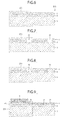
- les
figures 1 à 16 ont trait à différents modes de mise en oeuvre du procédé selon l'invention et de réalisation d'un dispositif selon l'invention. - Sur la
figure 1 , la référence DIS désigne un dispositif, par exemple une plaquette semi-conductrice (wafer) comportant une région inférieure, ou substrat support, 3 de silicium non contraint. Cette région 3 peut être par exemple un caisson. - Cette région 3 peut généralement comprendre du silicium intrinsèque, c'est-à-dire non dopé. Cela étant, en pratique, il existe toujours un faible taux de dopants mais, lorsque ce taux de dopants est inférieur à 1015 atomes par cm3, on parle alors néanmoins de silicium intrinsèque.
- Cette région inférieure 3 de silicium est surmontée par une couche isolante enterrée 2 communément désignée par l'homme du métier sous la dénomination anglo-saxonne de « BOX ». Cette région isolante peut être par exemple formée de dioxyde de silicium.
- Au-dessus de cette couche isolante enterrée, se situe un film semi-conducteur 1 formé ici de silicium contraint en tension. On voit donc ici que le film 1 fait partie d'un substrat du type silicium sur isolant.
- Dans une technologie FD SOI, l'épaisseur de ce film 1 est de l'ordre de quelques nanomètres. Et, c'est dans ce film 1 que vont être réalisés des transistors NMOS et PMOS.
- On va maintenant décrire en se référant plus particulièrement aux
figures 2 à 5 , un mode de mise en oeuvre du procédé permettant de relâcher localement les contraintes en tension dans le film semi-conducteur 1. - A cet égard, comme illustré sur la
figure 2 , on forme dans le film 1 un orifice ou une ouverture 4, typiquement par une opération classique de gravure, qui se prolonge dans la couche isolante enterrée 2 pour déboucher sur la région inférieure 3 de silicium non contraint. - On procède ensuite (
figure 3 ) à une épitaxie classique et connue en soi 30 de silicium de façon à venir combler l'ouverture 4 par du silicium qui est cette fois-ci non contraint car ayant crû depuis la région 3 de silicium non contraint. - On procède ensuite (
figure 4 ) à une amorphisation localisée du film 1 dans une zone contenant au moins une partie de l'ouverture avec le silicium épitaxié, de façon à former une zone amorphisée 11 au contact du silicium épitaxié ayant comblé ladite ouverture. La définition de l'emplacement de cette zone s'effectue de façon classique par un masque et l'amorphisation comprend, de façon classique, un bombardement de la zone de silicium correspondante par des atomes, par exemple de l'argon ou du germanium. - A l'issue de cette amorphisation, le film 1 comporte par conséquent une zone amorphisée localisée 11 qui est en contact avec le silicium non contraint 31 résultant de l'épitaxie 30 et situé entre les portions de couche isolante 2.
- Le film 1 comporte également de part et d'autre de cette zone amorphisée 11 une zone de film 10 formée de silicium contraint en tension.
- L'étape suivante (
figure 5 ) comprend une recristallisation de la zone amorphisée 11 par une épitaxie en phase solide 50. Une telle épitaxie est connue par l'homme du métier sous l'acronyme anglosaxon de « SPER » (« Solide Phase Epitaxy Regrowth »). - Une telle épitaxie est obtenue à partir du germe de silicium non contraint 31 par chauffage, typiquement entre 400 et 1000°C pendant une durée pouvant varier entre une minute et une heure selon le volume de la zone amorphisée à recristalliser. L'homme du métier pourra à toutes fins utiles se référer, en ce qui concerne notamment des ordres de grandeurs des vitesses de recristallisation du silicium amorphisé à l'article suivant : « Substrate-orientation dependence of the epitaxial regrowth rate from Si-implanted amorphous Si », L. Csepregi et al, J. Appl. Phys. 49(7), pp 3906-3911, July 1978 .
- A l'issue de cette recristallisation, le film 1 comporte une zone localisée 12 de film comportant du silicium relâché en tension, et une zone de film 10 comportant du silicium contraint en tension.
- On se réfère maintenant plus particulièrement aux
figures 6 à 12 pour décrire une application de l'invention à la co-intégration de transistors NMOS et de transistors PMOS dans un substrat du type FD SOI. - Plus précisément, comme illustré sur la
figure 6 , on souhaite réaliser les transistors NMOS dans la zone ZS1 du film 1 initialement contraint en tension et les transistors PMOS à l'extérieur de cette zone ZS1. - On procède alors (
figure 7 ) à la réalisation de deux ouvertures ou orifices 41 et 42 dans le film 1 et la couche isolante enterrée 2 débouchant dans la région inférieure de silicium (substrat support) 3, d'une façon analogue à ce qui a été décrit en référence à lafigure 2 . Il convient de noter ici que l'emplacement de ces deux ouvertures correspond aux deux emplacements des futurs puits de contact qui vont permettre de contacter le caisson inférieur 3 à partir de la face avant de façon à venir polariser les électrodes enterrées respectives qui seront formées par implantation sous la couche isolante 2. - On procède ensuite, d'une façon analogue à ce qui a été décrit en référence à la
figure 3 , à une épitaxie de silicium à partir de la région 3 de façon à venir combler les ouvertures 41 et 42 avec du silicium non contraint 31 et 32 (figure 8 ). - Puis, comme illustré sur la
figure 9 , on masque la zone de silicium contraint 10 du film 1, destiné à recevoir le ou les transistors NMOS, avec un bloc de résine 6 avant de procéder à l'amorphisation localisée du reste du film 1. - On obtient donc une zone amorphisée 11 en contact notamment avec le silicium non contraint 31.
- On procède ensuite (
figure 10 ) à une recristallisation de la zone amorphisée 11 à partir notamment du silicium non contraint 31 de façon à former une zone localisée 12 de film comportant du silicium relâché en tension. - On procède ensuite à la réalisation classique de zones d'isolation 7 du type tranchées peu profondes par exemple (en anglais STI), de façon à isoler électriquement les zones de film 10 et 12 et à délimiter les puits de contact 81 et 82 (
figure 11 ) qui vont permettre la polarisation des électrodes enterrées (non représentées ici à des fins de simplification) depuis une face supérieure F1 du film 1. - Comme illustré sur la
figure 12 , un ou plusieurs transistors NMOS TN sont réalisés dans la zone de film 10 comportant du silicium contraint en tension, les régions de source S et de drain D du ou des transistors étant réalisées par une epitaxie suivie d'une implantation de dopants, ou par une épitaxie de semi-conducteur (par exemple Silicium) dopée in-situ (par exemple Carbone ou Phosphore). - Par ailleurs, le ou les transistors PMOS TP sont réalisés dans la zone de silicium relâchée en contrainte de tension 12. De la même façon que pour le NMOS TN, les régions de source S et drain D seront réalisé par implantation de dopants, ou par une épitaxie de semi-conducteur (par exemple Silicium ou Silicium Germanium) dopée in-situ (par exemple Bore).
- Bien entendu si la région 11 de silicium amorphisée est trop longue, il se peut que la recristallisation de cette zone soit incomplète. Dans ce cas on prévoira au préalable plusieurs orifices de « germination», sous cette grande zone amorphisée ce qui va conduire in fine à plusieurs zones 12 séparées par des puits de contact, dans lesquelles seront réalisés les transistors PMOS..
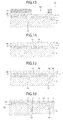
- Les
figures 13 à 16 illustrent schématiquement une autre mise en oeuvre de l'invention prévoyant cette fois-ci la réalisation d'une zone localisée de film contraint en compression. - Plus précisément, sur la structure illustrée sur la
figure 10 , on dépose une couche de masque dur 90 ainsi qu'un bloc de résine 91. - On délimite ensuite par masquage, l'emplacement d'un orifice ou d'une ouverture 92 permettant de dégager la partie de la zone 12 de silicium relâchée en tension dans laquelle vont être réalisés les transistors PMOS.
- On fait croître ensuite (
figure 14 ) une couche 93 d'un alliage de silicium germanium. Une telle étape d'épitaxie de SiGe est classique et connue en soi. Puis, on procède à une étape de condensation de ce silicium germanium conduisant à une oxydation surfacique du silicium germanium et à une diffusion des atomes de germanium dans la couche de silicium sous jacente 12. - Une telle étape de condensation, classique et connue en soi, s'effectue en chauffant le silicium germanium épitaxié par exemple à une température de 900°C à 1100°C pendant une durée de l'ordre de la seconde à quelques minutes.
- A l'issue de cette étape de condensation, le dispositif DIS comporte une couche de silicium germanium contraint en compression surmonté d'une couche de dioxyde de silicium 94 (
figure 15 ). - On procède ensuite (
figure 16 ) à un retrait du masque dur 90 et de la couche de dioxyde de silicium 94 par un nettoyage classique, par exemple à l'aide d'acide fluorhydrique. - Après réalisation des tranchées isolantes 7, on obtient donc un dispositif comportant dans la zone ZS1 un film de silicium contraint en tension 10 dans laquelle va pouvoir être réalisé le ou les transistors NMOS ainsi qu'un film 13 en silicium germanium contraint en compression, dans lequel va pouvoir être réalisé le ou les transistors PMOS.
- Il convient de noter qu'une zone contrainte en tension (resp. en compression) dans une direction est contrainte en compression (resp. en tension) dans une direction perpendiculaire. Une zone ne peut pas être contrainte en tension et en compression suivant la même direction.
Claims (9)
- Procédé de modification localisée des contraintes dans un substrat du type silicium sur isolant initialement contraint en tension comprenant un film semi-conducteur de silicium initialement contraint en tension disposé sur une couche isolante dite enterrée elle-même disposée sur un substrat support de silicium non contraint, le procédé comprenant :une formation d'au moins une ouverture (4) dans le film (1) de silicium initialement contraint et dans la couche isolante enterrée sous-jacente (2) jusqu'à atteindre le substrat (3) de silicium non contraint,une épitaxie (30) de silicium dans ledit au moins une ouverture (4) à partir du substrat support (3) de silicium non contraint de façon à combler ladite au moins une ouverture,une amorphisation localisée d'une zone dudit film de silicium incluant ladite au moins une zone épitaxiée (31), etune recristallisation de ladite au moins une zone amorphisée (11) par une épitaxie en phase solide (50) à partir de la partie de silicium non contraint (31) située dans ledit au moins un orifice et en contact avec la zone amorphisée (11), de façon à obtenir dans le film (1) de silicium contraint au moins une zone localisée de film (12) comportant du silicium relâché en tension.
- Procédé selon la revendication 1, dans lequel le substrat (1) est de type silicium sur isolant totalement déserté initialement contraint en tension.
- Procédé selon la revendication 2, dans lequel ladite ouverture (41) est formée au niveau d'un puits (81) destiné à permettre un contact avec le substrat support de silicium depuis la face supérieure du film (1).
- Procédé selon l'une des revendications précédentes, comprenant en outre une formation d'un alliage de silicium germanium (13) dans au moins une partie de ladite zone localisée relâchée en tension, de façon à former une zone de film contraint en compression (13).
- Procédé de réalisation de transistors du type à canal N et de transistors du type à canal P dans un substrat de type silicium sur isolant initialement contraint comprenant un film semi-conducteur de silicium initialement contraint en tension disposé sur une couche isolante dite enterrée elle-même disposée sur un substrat support de silicium non contraint, le procédé comprenant
une réalisation des transistors à canal P dans ladite au moins une zone localisée de silicium relâché en tension (12) obtenue par le procédé selon l'une des revendications 1 à 3 ou dans la zone de film contrainte en compression (13) obtenue par le procédé selon la revendication 4, et
une réalisation des transistors à canal N dans la ou les zones de film (10) comportant du silicium contraint en tension. - Dispositif comprenant un substrat du type silicium sur isolant comportant un film semi-conducteur (1) disposé sur une couche isolante (2) dite enterrée elle-même disposée sur un substrat support de silicium non contraint (3), le film semi-conducteur comportant au moins une première zone de film (10) comportant du silicium contraint en tension et au moins une deuxième zone de film (12) comportant du silicium relâché en tension, ladite couche isolante enterrée (2) comportant au moins une ouverture sous ladite au moins une deuxième zone de film (12), ladite ouverture comportant du silicium non contraint (31).
- Dispositif selon la revendication 6, dans lequel le substrat (1) est du type silicium sur isolant totalement déserté.
- Dispositif selon la revendication 6 ou 7, dans lequel au moins une partie de ladite au moins une deuxième zone de film comprend un alliage de silicium germanium de façon à former une partie de film contraint en compression (13).
- Dispositif selon l'une des revendications 6 à 8, comprenant au moins un transistor NMOS (TN) disposé dans et sur ladite au moins une première zone de substrat et au moins un transistor PMOS (TP) disposé dans et sur ladite deuxième zone de substrat.
Applications Claiming Priority (1)
| Application Number | Priority Date | Filing Date | Title |
|---|---|---|---|
| FR1352535A FR3003685B1 (fr) | 2013-03-21 | 2013-03-21 | Procede de modification localisee des contraintes dans un substrat du type soi, en particulier fd soi, et dispositif correspondant |
Publications (2)
| Publication Number | Publication Date |
|---|---|
| EP2782119A1 true EP2782119A1 (fr) | 2014-09-24 |
| EP2782119B1 EP2782119B1 (fr) | 2021-03-31 |
Family
ID=48979879
Family Applications (1)
| Application Number | Title | Priority Date | Filing Date |
|---|---|---|---|
| EP14160802.6A Active EP2782119B1 (fr) | 2013-03-21 | 2014-03-20 | Procédé de modification localisée des contraintes dans un substrat du type soi, en particulier fd soi, et dispositif correspondant |
Country Status (3)
| Country | Link |
|---|---|
| US (2) | US9653538B2 (fr) |
| EP (1) | EP2782119B1 (fr) |
| FR (1) | FR3003685B1 (fr) |
Cited By (1)
| Publication number | Priority date | Publication date | Assignee | Title |
|---|---|---|---|---|
| EP3503175A1 (fr) * | 2017-12-22 | 2019-06-26 | Commissariat à l'énergie atomique et aux énergies alternatives | Procede de realisation d'un substrat semi-conducteur comprenant au moins une portion de semi-conducteur contraint en compression |
Families Citing this family (8)
| Publication number | Priority date | Publication date | Assignee | Title |
|---|---|---|---|---|
| US9437680B1 (en) * | 2015-03-31 | 2016-09-06 | International Business Machines Corporation | Silicon-on-insulator substrates having selectively formed strained and relaxed device regions |
| US9627536B2 (en) | 2015-06-25 | 2017-04-18 | International Busines Machines Corporation | Field effect transistors with strained channel features |
| US9559120B2 (en) | 2015-07-02 | 2017-01-31 | International Business Machines Corporation | Porous silicon relaxation medium for dislocation free CMOS devices |
| US9608068B2 (en) | 2015-08-05 | 2017-03-28 | International Business Machines Corporation | Substrate with strained and relaxed silicon regions |
| US11251042B2 (en) * | 2019-10-31 | 2022-02-15 | Taiwan Semiconductor Manufacturing Co., Ltd. | Formation of single crystal semiconductors using planar vapor liquid solid epitaxy |
| FR3109838B1 (fr) | 2020-04-30 | 2022-05-20 | St Microelectronics Crolles 2 Sas | Transistors contraints et mémoire à changement de phase |
| CN113990955B (zh) | 2020-07-27 | 2025-12-16 | 意法半导体股份有限公司 | 具有减小的电压降的碳化硅二极管以及其制造方法 |
| IT202000018130A1 (it) | 2020-07-27 | 2022-01-27 | St Microelectronics Srl | Diodo in carburo di silicio con ridotta caduta di tensione, e relativo procedimento di fabbricazione |
Citations (3)
| Publication number | Priority date | Publication date | Assignee | Title |
|---|---|---|---|---|
| US20050116290A1 (en) * | 2003-12-02 | 2005-06-02 | De Souza Joel P. | Planar substrate with selected semiconductor crystal orientations formed by localized amorphization and recrystallization of stacked template layers |
| US20070281446A1 (en) * | 2006-05-31 | 2007-12-06 | Winstead Brian A | Dual surface SOI by lateral epitaxial overgrowth |
| US20090108301A1 (en) * | 2007-10-30 | 2009-04-30 | International Business Machines Corporation | Hybrid orientation semiconductor structure with reduced boundary defects and method of forming same |
Family Cites Families (13)
| Publication number | Priority date | Publication date | Assignee | Title |
|---|---|---|---|---|
| JP3488730B2 (ja) * | 1993-11-05 | 2004-01-19 | 株式会社ルネサステクノロジ | 半導体集積回路装置 |
| US6760200B2 (en) * | 2000-11-24 | 2004-07-06 | Alps Electric Co., Ltd. | Spin-valve thin-film magnetic element suitable for track narrowing and thin-film magnetic head using the same |
| DE102004060961B4 (de) * | 2004-12-17 | 2010-06-02 | Advanced Micro Devices, Inc., Sunnyvale | Verfahren zur Herstellung eines Hybridhalbleitersubstrats über einer vergrabenen Isolierschicht |
| US7432149B2 (en) * | 2005-06-23 | 2008-10-07 | Taiwan Semiconductor Manufacturing Company, Ltd. | CMOS on SOI substrates with hybrid crystal orientations |
| US7586158B2 (en) * | 2005-07-07 | 2009-09-08 | Infineon Technologies Ag | Piezoelectric stress liner for bulk and SOI |
| JP2007335573A (ja) * | 2006-06-14 | 2007-12-27 | Hitachi Ltd | 半導体装置およびその製造方法 |
| JP5132928B2 (ja) * | 2006-12-25 | 2013-01-30 | パナソニック株式会社 | 半導体装置 |
| US7534674B2 (en) * | 2007-04-19 | 2009-05-19 | Freescale Semiconductor, Inc. | Method of making a semiconductor device with a stressor |
| FR2915318B1 (fr) | 2007-04-20 | 2009-07-17 | St Microelectronics Crolles 2 | Procede de realisation d'un circuit electronique integre a deux portions de couches actives ayant des orientations cristallines differentes |
| US8273617B2 (en) * | 2009-09-30 | 2012-09-25 | Suvolta, Inc. | Electronic devices and systems, and methods for making and using the same |
| FR2975803B1 (fr) * | 2011-05-24 | 2014-01-10 | Commissariat Energie Atomique | Circuit integre realise en soi comprenant des cellules adjacentes de differents types |
| FR2980035B1 (fr) * | 2011-09-08 | 2013-10-04 | Commissariat Energie Atomique | Circuit integre realise en soi comprenant des cellules adjacentes de differents types |
| US9252208B1 (en) * | 2014-07-31 | 2016-02-02 | Stmicroelectronics, Inc. | Uniaxially-strained FD-SOI finFET |
-
2013
- 2013-03-21 FR FR1352535A patent/FR3003685B1/fr active Active
-
2014
- 2014-03-20 US US14/220,542 patent/US9653538B2/en active Active
- 2014-03-20 EP EP14160802.6A patent/EP2782119B1/fr active Active
-
2017
- 2017-04-10 US US15/483,299 patent/US10381478B2/en active Active
Patent Citations (3)
| Publication number | Priority date | Publication date | Assignee | Title |
|---|---|---|---|---|
| US20050116290A1 (en) * | 2003-12-02 | 2005-06-02 | De Souza Joel P. | Planar substrate with selected semiconductor crystal orientations formed by localized amorphization and recrystallization of stacked template layers |
| US20070281446A1 (en) * | 2006-05-31 | 2007-12-06 | Winstead Brian A | Dual surface SOI by lateral epitaxial overgrowth |
| US20090108301A1 (en) * | 2007-10-30 | 2009-04-30 | International Business Machines Corporation | Hybrid orientation semiconductor structure with reduced boundary defects and method of forming same |
Non-Patent Citations (1)
| Title |
|---|
| L. CSEPREGI ET AL.: "Substrate-orientation dependence of the epitaxial regrowth rate from Si-implanted amorphous Si", J. APPL. PHYS., vol. 49, no. 7, July 1978 (1978-07-01), pages 3906 - 3911 |
Cited By (1)
| Publication number | Priority date | Publication date | Assignee | Title |
|---|---|---|---|---|
| EP3503175A1 (fr) * | 2017-12-22 | 2019-06-26 | Commissariat à l'énergie atomique et aux énergies alternatives | Procede de realisation d'un substrat semi-conducteur comprenant au moins une portion de semi-conducteur contraint en compression |
Also Published As
| Publication number | Publication date |
|---|---|
| EP2782119B1 (fr) | 2021-03-31 |
| US9653538B2 (en) | 2017-05-16 |
| US10381478B2 (en) | 2019-08-13 |
| US20150021692A1 (en) | 2015-01-22 |
| FR3003685A1 (fr) | 2014-09-26 |
| US20170213910A1 (en) | 2017-07-27 |
| FR3003685B1 (fr) | 2015-04-17 |
Similar Documents
| Publication | Publication Date | Title |
|---|---|---|
| EP2782119B1 (fr) | Procédé de modification localisée des contraintes dans un substrat du type soi, en particulier fd soi, et dispositif correspondant | |
| EP2887384B1 (fr) | Procédé amélioré de réalisation de blocs semi-conducteurs contraints sur la couche isolante d'un substrat semi-conducteur sur isolant | |
| FR2821483A1 (fr) | Procede de fabrication d'un transistor a grille isolee et a architecture du type substrat sur isolant, et transistor correspondant | |
| EP2975646B1 (fr) | Procede de fabrication d'un transistor dans lequel le niveau de contrainte applique au canal est augmente | |
| EP2840594A2 (fr) | Recristallisation de blocs de source et de drain par le haut | |
| EP2610915A1 (fr) | Transistor et procédé de fabrication d'un transistor | |
| EP3142151B1 (fr) | Procede de realisation d'une structure de canal de transistor en contrainte uni-axiale | |
| FR2979480A1 (fr) | Procede de realisation d'un dispositif a transistors contraints par siliciuration des zones de source et de drain | |
| WO2014037411A1 (fr) | Procédé de réalisation de transistors fet | |
| EP1638149B1 (fr) | Procédé de fabrication d'un transistor à effet de champ à grille isolée à canal à hétérostructure | |
| EP2765599A1 (fr) | Procédé de fabrication d'un transistor | |
| FR3047352A1 (fr) | Procede de fabrication d'un transistor a dopant localise a l'aplomb de la grille | |
| EP1808890A1 (fr) | Procédé de réalisation d'une couche monocristalline sur une couche diélectrique | |
| FR2806833A1 (fr) | Procede de fabrication d'un transistor mos a deux grilles, dont l'une est enterree, et transistor correspondant | |
| EP1788635B1 (fr) | Procédé de réalisation de transistor à double grilles auto-alignées par réduction de motifs de grille | |
| FR2896338A1 (fr) | Procede de realisation d'une couche monocristalline sur une couche dielectrique | |
| EP2562803B1 (fr) | Procédé de réalisation d'un dispositif à transistors contraints à l'aide d'une couche externe, et dispositif | |
| EP3671826B1 (fr) | Procédé amélioré de fabrication d'un circuit intégré comportant un transistor nmos et un transistor pmos | |
| FR2915318A1 (fr) | Procede de realisation d'un circuit electronique integre a deux portions de couches actives ayant des orientations cristallines differentes | |
| FR3036846A1 (fr) | Procede d'isolation locale entre des transistors realises sur un substrat soi, en particulier fdsoi, et circuit integre correspondant | |
| FR3035265A1 (fr) | Procede de fabrication de transistors soi pour une densite d'integration accrue | |
| EP3671836B1 (fr) | Circuit 3d dote d'une isolation mesa pour la zone de plan de masse | |
| FR2827705A1 (fr) | Transistor et procede de fabrication d'un transistor sur un substrat sige/soi | |
| FR2819631A1 (fr) | Procede de fabrication d'un substrat monocristallin, et circuit integre comportant un tel substrat | |
| EP1746643B1 (fr) | Procédé de réalisation d'un transistor MOS. |
Legal Events
| Date | Code | Title | Description |
|---|---|---|---|
| PUAI | Public reference made under article 153(3) epc to a published international application that has entered the european phase |
Free format text: ORIGINAL CODE: 0009012 |
|
| 17P | Request for examination filed |
Effective date: 20140320 |
|
| AK | Designated contracting states |
Kind code of ref document: A1 Designated state(s): AL AT BE BG CH CY CZ DE DK EE ES FI FR GB GR HR HU IE IS IT LI LT LU LV MC MK MT NL NO PL PT RO RS SE SI SK SM TR |
|
| AX | Request for extension of the european patent |
Extension state: BA ME |
|
| R17P | Request for examination filed (corrected) |
Effective date: 20150320 |
|
| STAA | Information on the status of an ep patent application or granted ep patent |
Free format text: STATUS: EXAMINATION IS IN PROGRESS |
|
| 17Q | First examination report despatched |
Effective date: 20190430 |
|
| GRAP | Despatch of communication of intention to grant a patent |
Free format text: ORIGINAL CODE: EPIDOSNIGR1 |
|
| STAA | Information on the status of an ep patent application or granted ep patent |
Free format text: STATUS: GRANT OF PATENT IS INTENDED |
|
| INTG | Intention to grant announced |
Effective date: 20200604 |
|
| GRAJ | Information related to disapproval of communication of intention to grant by the applicant or resumption of examination proceedings by the epo deleted |
Free format text: ORIGINAL CODE: EPIDOSDIGR1 |
|
| STAA | Information on the status of an ep patent application or granted ep patent |
Free format text: STATUS: EXAMINATION IS IN PROGRESS |
|
| INTC | Intention to grant announced (deleted) | ||
| GRAP | Despatch of communication of intention to grant a patent |
Free format text: ORIGINAL CODE: EPIDOSNIGR1 |
|
| STAA | Information on the status of an ep patent application or granted ep patent |
Free format text: STATUS: GRANT OF PATENT IS INTENDED |
|
| INTG | Intention to grant announced |
Effective date: 20201104 |
|
| GRAS | Grant fee paid |
Free format text: ORIGINAL CODE: EPIDOSNIGR3 |
|
| GRAA | (expected) grant |
Free format text: ORIGINAL CODE: 0009210 |
|
| STAA | Information on the status of an ep patent application or granted ep patent |
Free format text: STATUS: THE PATENT HAS BEEN GRANTED |
|
| AK | Designated contracting states |
Kind code of ref document: B1 Designated state(s): AL AT BE BG CH CY CZ DE DK EE ES FI FR GB GR HR HU IE IS IT LI LT LU LV MC MK MT NL NO PL PT RO RS SE SI SK SM TR |
|
| REG | Reference to a national code |
Ref country code: GB Ref legal event code: FG4D Free format text: NOT ENGLISH Ref country code: CH Ref legal event code: EP |
|
| REG | Reference to a national code |
Ref country code: AT Ref legal event code: REF Ref document number: 1377891 Country of ref document: AT Kind code of ref document: T Effective date: 20210415 |
|
| REG | Reference to a national code |
Ref country code: DE Ref legal event code: R096 Ref document number: 602014076101 Country of ref document: DE |
|
| REG | Reference to a national code |
Ref country code: IE Ref legal event code: FG4D Free format text: LANGUAGE OF EP DOCUMENT: FRENCH |
|
| REG | Reference to a national code |
Ref country code: LT Ref legal event code: MG9D |
|
| PG25 | Lapsed in a contracting state [announced via postgrant information from national office to epo] |
Ref country code: NO Free format text: LAPSE BECAUSE OF FAILURE TO SUBMIT A TRANSLATION OF THE DESCRIPTION OR TO PAY THE FEE WITHIN THE PRESCRIBED TIME-LIMIT Effective date: 20210630 Ref country code: BG Free format text: LAPSE BECAUSE OF FAILURE TO SUBMIT A TRANSLATION OF THE DESCRIPTION OR TO PAY THE FEE WITHIN THE PRESCRIBED TIME-LIMIT Effective date: 20210630 Ref country code: HR Free format text: LAPSE BECAUSE OF FAILURE TO SUBMIT A TRANSLATION OF THE DESCRIPTION OR TO PAY THE FEE WITHIN THE PRESCRIBED TIME-LIMIT Effective date: 20210331 Ref country code: FI Free format text: LAPSE BECAUSE OF FAILURE TO SUBMIT A TRANSLATION OF THE DESCRIPTION OR TO PAY THE FEE WITHIN THE PRESCRIBED TIME-LIMIT Effective date: 20210331 |
|
| PG25 | Lapsed in a contracting state [announced via postgrant information from national office to epo] |
Ref country code: RS Free format text: LAPSE BECAUSE OF FAILURE TO SUBMIT A TRANSLATION OF THE DESCRIPTION OR TO PAY THE FEE WITHIN THE PRESCRIBED TIME-LIMIT Effective date: 20210331 Ref country code: LV Free format text: LAPSE BECAUSE OF FAILURE TO SUBMIT A TRANSLATION OF THE DESCRIPTION OR TO PAY THE FEE WITHIN THE PRESCRIBED TIME-LIMIT Effective date: 20210331 Ref country code: SE Free format text: LAPSE BECAUSE OF FAILURE TO SUBMIT A TRANSLATION OF THE DESCRIPTION OR TO PAY THE FEE WITHIN THE PRESCRIBED TIME-LIMIT Effective date: 20210331 |
|
| REG | Reference to a national code |
Ref country code: NL Ref legal event code: MP Effective date: 20210331 |
|
| REG | Reference to a national code |
Ref country code: AT Ref legal event code: MK05 Ref document number: 1377891 Country of ref document: AT Kind code of ref document: T Effective date: 20210331 |
|
| PG25 | Lapsed in a contracting state [announced via postgrant information from national office to epo] |
Ref country code: SM Free format text: LAPSE BECAUSE OF FAILURE TO SUBMIT A TRANSLATION OF THE DESCRIPTION OR TO PAY THE FEE WITHIN THE PRESCRIBED TIME-LIMIT Effective date: 20210331 Ref country code: AT Free format text: LAPSE BECAUSE OF FAILURE TO SUBMIT A TRANSLATION OF THE DESCRIPTION OR TO PAY THE FEE WITHIN THE PRESCRIBED TIME-LIMIT Effective date: 20210331 Ref country code: CZ Free format text: LAPSE BECAUSE OF FAILURE TO SUBMIT A TRANSLATION OF THE DESCRIPTION OR TO PAY THE FEE WITHIN THE PRESCRIBED TIME-LIMIT Effective date: 20210331 Ref country code: EE Free format text: LAPSE BECAUSE OF FAILURE TO SUBMIT A TRANSLATION OF THE DESCRIPTION OR TO PAY THE FEE WITHIN THE PRESCRIBED TIME-LIMIT Effective date: 20210331 Ref country code: LT Free format text: LAPSE BECAUSE OF FAILURE TO SUBMIT A TRANSLATION OF THE DESCRIPTION OR TO PAY THE FEE WITHIN THE PRESCRIBED TIME-LIMIT Effective date: 20210331 Ref country code: NL Free format text: LAPSE BECAUSE OF FAILURE TO SUBMIT A TRANSLATION OF THE DESCRIPTION OR TO PAY THE FEE WITHIN THE PRESCRIBED TIME-LIMIT Effective date: 20210331 |
|
| PG25 | Lapsed in a contracting state [announced via postgrant information from national office to epo] |
Ref country code: IS Free format text: LAPSE BECAUSE OF FAILURE TO SUBMIT A TRANSLATION OF THE DESCRIPTION OR TO PAY THE FEE WITHIN THE PRESCRIBED TIME-LIMIT Effective date: 20210731 Ref country code: PL Free format text: LAPSE BECAUSE OF FAILURE TO SUBMIT A TRANSLATION OF THE DESCRIPTION OR TO PAY THE FEE WITHIN THE PRESCRIBED TIME-LIMIT Effective date: 20210331 Ref country code: PT Free format text: LAPSE BECAUSE OF FAILURE TO SUBMIT A TRANSLATION OF THE DESCRIPTION OR TO PAY THE FEE WITHIN THE PRESCRIBED TIME-LIMIT Effective date: 20210802 Ref country code: ES Free format text: LAPSE BECAUSE OF FAILURE TO SUBMIT A TRANSLATION OF THE DESCRIPTION OR TO PAY THE FEE WITHIN THE PRESCRIBED TIME-LIMIT Effective date: 20210331 Ref country code: RO Free format text: LAPSE BECAUSE OF FAILURE TO SUBMIT A TRANSLATION OF THE DESCRIPTION OR TO PAY THE FEE WITHIN THE PRESCRIBED TIME-LIMIT Effective date: 20210331 Ref country code: SK Free format text: LAPSE BECAUSE OF FAILURE TO SUBMIT A TRANSLATION OF THE DESCRIPTION OR TO PAY THE FEE WITHIN THE PRESCRIBED TIME-LIMIT Effective date: 20210331 |
|
| REG | Reference to a national code |
Ref country code: DE Ref legal event code: R097 Ref document number: 602014076101 Country of ref document: DE |
|
| PG25 | Lapsed in a contracting state [announced via postgrant information from national office to epo] |
Ref country code: DK Free format text: LAPSE BECAUSE OF FAILURE TO SUBMIT A TRANSLATION OF THE DESCRIPTION OR TO PAY THE FEE WITHIN THE PRESCRIBED TIME-LIMIT Effective date: 20210331 Ref country code: AL Free format text: LAPSE BECAUSE OF FAILURE TO SUBMIT A TRANSLATION OF THE DESCRIPTION OR TO PAY THE FEE WITHIN THE PRESCRIBED TIME-LIMIT Effective date: 20210331 |
|
| PLBE | No opposition filed within time limit |
Free format text: ORIGINAL CODE: 0009261 |
|
| STAA | Information on the status of an ep patent application or granted ep patent |
Free format text: STATUS: NO OPPOSITION FILED WITHIN TIME LIMIT |
|
| 26N | No opposition filed |
Effective date: 20220104 |
|
| PG25 | Lapsed in a contracting state [announced via postgrant information from national office to epo] |
Ref country code: IS Free format text: LAPSE BECAUSE OF FAILURE TO SUBMIT A TRANSLATION OF THE DESCRIPTION OR TO PAY THE FEE WITHIN THE PRESCRIBED TIME-LIMIT Effective date: 20210731 |
|
| PG25 | Lapsed in a contracting state [announced via postgrant information from national office to epo] |
Ref country code: MC Free format text: LAPSE BECAUSE OF FAILURE TO SUBMIT A TRANSLATION OF THE DESCRIPTION OR TO PAY THE FEE WITHIN THE PRESCRIBED TIME-LIMIT Effective date: 20210331 |
|
| REG | Reference to a national code |
Ref country code: CH Ref legal event code: PL |
|
| REG | Reference to a national code |
Ref country code: BE Ref legal event code: MM Effective date: 20220331 |
|
| PG25 | Lapsed in a contracting state [announced via postgrant information from national office to epo] |
Ref country code: LU Free format text: LAPSE BECAUSE OF NON-PAYMENT OF DUE FEES Effective date: 20220320 Ref country code: LI Free format text: LAPSE BECAUSE OF NON-PAYMENT OF DUE FEES Effective date: 20220331 Ref country code: IE Free format text: LAPSE BECAUSE OF NON-PAYMENT OF DUE FEES Effective date: 20220320 Ref country code: CH Free format text: LAPSE BECAUSE OF NON-PAYMENT OF DUE FEES Effective date: 20220331 |
|
| PG25 | Lapsed in a contracting state [announced via postgrant information from national office to epo] |
Ref country code: BE Free format text: LAPSE BECAUSE OF NON-PAYMENT OF DUE FEES Effective date: 20220331 |
|
| PG25 | Lapsed in a contracting state [announced via postgrant information from national office to epo] |
Ref country code: HU Free format text: LAPSE BECAUSE OF FAILURE TO SUBMIT A TRANSLATION OF THE DESCRIPTION OR TO PAY THE FEE WITHIN THE PRESCRIBED TIME-LIMIT; INVALID AB INITIO Effective date: 20140320 |
|
| PG25 | Lapsed in a contracting state [announced via postgrant information from national office to epo] |
Ref country code: MK Free format text: LAPSE BECAUSE OF FAILURE TO SUBMIT A TRANSLATION OF THE DESCRIPTION OR TO PAY THE FEE WITHIN THE PRESCRIBED TIME-LIMIT Effective date: 20210331 Ref country code: CY Free format text: LAPSE BECAUSE OF FAILURE TO SUBMIT A TRANSLATION OF THE DESCRIPTION OR TO PAY THE FEE WITHIN THE PRESCRIBED TIME-LIMIT Effective date: 20210331 |
|
| PGFP | Annual fee paid to national office [announced via postgrant information from national office to epo] |
Ref country code: GB Payment date: 20240325 Year of fee payment: 11 |
|
| PGFP | Annual fee paid to national office [announced via postgrant information from national office to epo] |
Ref country code: IT Payment date: 20240312 Year of fee payment: 11 |
|
| PG25 | Lapsed in a contracting state [announced via postgrant information from national office to epo] |
Ref country code: TR Free format text: LAPSE BECAUSE OF FAILURE TO SUBMIT A TRANSLATION OF THE DESCRIPTION OR TO PAY THE FEE WITHIN THE PRESCRIBED TIME-LIMIT Effective date: 20210331 |
|
| PG25 | Lapsed in a contracting state [announced via postgrant information from national office to epo] |
Ref country code: MT Free format text: LAPSE BECAUSE OF FAILURE TO SUBMIT A TRANSLATION OF THE DESCRIPTION OR TO PAY THE FEE WITHIN THE PRESCRIBED TIME-LIMIT Effective date: 20210331 |
|
| PG25 | Lapsed in a contracting state [announced via postgrant information from national office to epo] |
Ref country code: GR Free format text: LAPSE BECAUSE OF NON-PAYMENT OF DUE FEES Effective date: 20210331 |
|
| PG25 | Lapsed in a contracting state [announced via postgrant information from national office to epo] |
Ref country code: GR Free format text: LAPSE BECAUSE OF NON-PAYMENT OF DUE FEES Effective date: 20210331 |
|
| GBPC | Gb: european patent ceased through non-payment of renewal fee |
Effective date: 20250320 |
|
| REG | Reference to a national code |
Ref country code: DE Ref legal event code: R079 Ref document number: 602014076101 Country of ref document: DE Free format text: PREVIOUS MAIN CLASS: H01L0021200000 Ipc: H10P0014200000 |
|
| PG25 | Lapsed in a contracting state [announced via postgrant information from national office to epo] |
Ref country code: GB Free format text: LAPSE BECAUSE OF NON-PAYMENT OF DUE FEES Effective date: 20250320 |
|
| PG25 | Lapsed in a contracting state [announced via postgrant information from national office to epo] |
Ref country code: IT Free format text: LAPSE BECAUSE OF NON-PAYMENT OF DUE FEES Effective date: 20250320 |
|
| PGFP | Annual fee paid to national office [announced via postgrant information from national office to epo] |
Ref country code: DE Payment date: 20260313 Year of fee payment: 13 |
|
| PGFP | Annual fee paid to national office [announced via postgrant information from national office to epo] |
Ref country code: FR Payment date: 20260331 Year of fee payment: 13 |