EP2774263B1 - Redundante zelle-zu-netz-fotovoltaikanlage - Google Patents
Redundante zelle-zu-netz-fotovoltaikanlage Download PDFInfo
- Publication number
- EP2774263B1 EP2774263B1 EP12846494.8A EP12846494A EP2774263B1 EP 2774263 B1 EP2774263 B1 EP 2774263B1 EP 12846494 A EP12846494 A EP 12846494A EP 2774263 B1 EP2774263 B1 EP 2774263B1
- Authority
- EP
- European Patent Office
- Prior art keywords
- module
- photovoltaic
- bus
- converters
- cells
- Prior art date
- Legal status (The legal status is an assumption and is not a legal conclusion. Google has not performed a legal analysis and makes no representation as to the accuracy of the status listed.)
- Active
Links
- 230000003287 optical effect Effects 0.000 claims description 19
- 238000004146 energy storage Methods 0.000 claims description 17
- 238000005259 measurement Methods 0.000 claims description 16
- 230000008878 coupling Effects 0.000 claims description 9
- 238000010168 coupling process Methods 0.000 claims description 9
- 238000005859 coupling reaction Methods 0.000 claims description 9
- 238000005286 illumination Methods 0.000 claims description 6
- 239000000853 adhesive Substances 0.000 claims description 5
- 230000001070 adhesive effect Effects 0.000 claims description 5
- 238000013480 data collection Methods 0.000 claims description 5
- 230000004044 response Effects 0.000 claims description 2
- 239000010410 layer Substances 0.000 description 12
- RYGMFSIKBFXOCR-UHFFFAOYSA-N Copper Chemical compound [Cu] RYGMFSIKBFXOCR-UHFFFAOYSA-N 0.000 description 10
- 229910052802 copper Inorganic materials 0.000 description 10
- 239000010949 copper Substances 0.000 description 10
- 239000000463 material Substances 0.000 description 9
- 238000003860 storage Methods 0.000 description 6
- 239000012790 adhesive layer Substances 0.000 description 5
- 239000004020 conductor Substances 0.000 description 5
- 238000000034 method Methods 0.000 description 5
- -1 but not limited to Substances 0.000 description 4
- 230000008859 change Effects 0.000 description 4
- 230000006870 function Effects 0.000 description 4
- 230000000670 limiting effect Effects 0.000 description 4
- 229920000139 polyethylene terephthalate Polymers 0.000 description 4
- 239000005020 polyethylene terephthalate Substances 0.000 description 4
- ATJFFYVFTNAWJD-UHFFFAOYSA-N Tin Chemical compound [Sn] ATJFFYVFTNAWJD-UHFFFAOYSA-N 0.000 description 3
- 229910052782 aluminium Inorganic materials 0.000 description 3
- XAGFODPZIPBFFR-UHFFFAOYSA-N aluminium Chemical compound [Al] XAGFODPZIPBFFR-UHFFFAOYSA-N 0.000 description 3
- 239000003990 capacitor Substances 0.000 description 3
- 238000005520 cutting process Methods 0.000 description 3
- 230000003247 decreasing effect Effects 0.000 description 3
- 229920000642 polymer Polymers 0.000 description 3
- 238000007789 sealing Methods 0.000 description 3
- 229930040373 Paraformaldehyde Natural products 0.000 description 2
- 239000011324 bead Substances 0.000 description 2
- 238000004891 communication Methods 0.000 description 2
- 230000001143 conditioned effect Effects 0.000 description 2
- 239000000356 contaminant Substances 0.000 description 2
- 230000007423 decrease Effects 0.000 description 2
- 238000010586 diagram Methods 0.000 description 2
- 230000007613 environmental effect Effects 0.000 description 2
- 239000005038 ethylene vinyl acetate Substances 0.000 description 2
- 238000009434 installation Methods 0.000 description 2
- 238000012423 maintenance Methods 0.000 description 2
- 238000004519 manufacturing process Methods 0.000 description 2
- 229910052751 metal Inorganic materials 0.000 description 2
- 239000002184 metal Substances 0.000 description 2
- 229910001092 metal group alloy Inorganic materials 0.000 description 2
- 230000000737 periodic effect Effects 0.000 description 2
- 229920006324 polyoxymethylene Polymers 0.000 description 2
- 229920001296 polysiloxane Polymers 0.000 description 2
- 230000008569 process Effects 0.000 description 2
- 230000005855 radiation Effects 0.000 description 2
- 230000008439 repair process Effects 0.000 description 2
- 230000002441 reversible effect Effects 0.000 description 2
- 239000000565 sealant Substances 0.000 description 2
- 238000012546 transfer Methods 0.000 description 2
- 229920004943 Delrin® Polymers 0.000 description 1
- 229910052790 beryllium Inorganic materials 0.000 description 1
- ATBAMAFKBVZNFJ-UHFFFAOYSA-N beryllium atom Chemical compound [Be] ATBAMAFKBVZNFJ-UHFFFAOYSA-N 0.000 description 1
- DQXBYHZEEUGOBF-UHFFFAOYSA-N but-3-enoic acid;ethene Chemical compound C=C.OC(=O)CC=C DQXBYHZEEUGOBF-UHFFFAOYSA-N 0.000 description 1
- 238000006243 chemical reaction Methods 0.000 description 1
- 238000012790 confirmation Methods 0.000 description 1
- 238000001816 cooling Methods 0.000 description 1
- 230000001186 cumulative effect Effects 0.000 description 1
- 230000001351 cycling effect Effects 0.000 description 1
- 230000009365 direct transmission Effects 0.000 description 1
- 238000009826 distribution Methods 0.000 description 1
- 230000000694 effects Effects 0.000 description 1
- 239000012777 electrically insulating material Substances 0.000 description 1
- 238000005516 engineering process Methods 0.000 description 1
- 230000005669 field effect Effects 0.000 description 1
- 239000011521 glass Substances 0.000 description 1
- 239000011213 glass-filled polymer Substances 0.000 description 1
- 239000004519 grease Substances 0.000 description 1
- 230000003116 impacting effect Effects 0.000 description 1
- 230000006872 improvement Effects 0.000 description 1
- 239000010445 mica Substances 0.000 description 1
- 229910052618 mica group Inorganic materials 0.000 description 1
- 238000012986 modification Methods 0.000 description 1
- 230000004048 modification Effects 0.000 description 1
- 238000012544 monitoring process Methods 0.000 description 1
- 239000004033 plastic Substances 0.000 description 1
- 229920003023 plastic Polymers 0.000 description 1
- 229920001200 poly(ethylene-vinyl acetate) Polymers 0.000 description 1
- 238000012545 processing Methods 0.000 description 1
- 230000001681 protective effect Effects 0.000 description 1
- 230000002829 reductive effect Effects 0.000 description 1
- 238000010079 rubber tapping Methods 0.000 description 1
- 239000004065 semiconductor Substances 0.000 description 1
- 238000005476 soldering Methods 0.000 description 1
- 239000007787 solid Substances 0.000 description 1
- 125000006850 spacer group Chemical group 0.000 description 1
- 230000003068 static effect Effects 0.000 description 1
- 239000003351 stiffener Substances 0.000 description 1
- 239000000126 substance Substances 0.000 description 1
- 239000000758 substrate Substances 0.000 description 1
- 238000011144 upstream manufacturing Methods 0.000 description 1
Images


Classifications
-
- H—ELECTRICITY
- H01—ELECTRIC ELEMENTS
- H01L—SEMICONDUCTOR DEVICES NOT COVERED BY CLASS H10
- H01L31/00—Semiconductor devices sensitive to infrared radiation, light, electromagnetic radiation of shorter wavelength or corpuscular radiation and specially adapted either for the conversion of the energy of such radiation into electrical energy or for the control of electrical energy by such radiation; Processes or apparatus specially adapted for the manufacture or treatment thereof or of parts thereof; Details thereof
- H01L31/02—Details
- H01L31/02016—Circuit arrangements of general character for the devices
- H01L31/02019—Circuit arrangements of general character for the devices for devices characterised by at least one potential jump barrier or surface barrier
- H01L31/02021—Circuit arrangements of general character for the devices for devices characterised by at least one potential jump barrier or surface barrier for solar cells
-
- H—ELECTRICITY
- H01—ELECTRIC ELEMENTS
- H01L—SEMICONDUCTOR DEVICES NOT COVERED BY CLASS H10
- H01L31/00—Semiconductor devices sensitive to infrared radiation, light, electromagnetic radiation of shorter wavelength or corpuscular radiation and specially adapted either for the conversion of the energy of such radiation into electrical energy or for the control of electrical energy by such radiation; Processes or apparatus specially adapted for the manufacture or treatment thereof or of parts thereof; Details thereof
- H01L31/04—Semiconductor devices sensitive to infrared radiation, light, electromagnetic radiation of shorter wavelength or corpuscular radiation and specially adapted either for the conversion of the energy of such radiation into electrical energy or for the control of electrical energy by such radiation; Processes or apparatus specially adapted for the manufacture or treatment thereof or of parts thereof; Details thereof adapted as photovoltaic [PV] conversion devices
- H01L31/042—PV modules or arrays of single PV cells
- H01L31/048—Encapsulation of modules
-
- H—ELECTRICITY
- H01—ELECTRIC ELEMENTS
- H01L—SEMICONDUCTOR DEVICES NOT COVERED BY CLASS H10
- H01L31/00—Semiconductor devices sensitive to infrared radiation, light, electromagnetic radiation of shorter wavelength or corpuscular radiation and specially adapted either for the conversion of the energy of such radiation into electrical energy or for the control of electrical energy by such radiation; Processes or apparatus specially adapted for the manufacture or treatment thereof or of parts thereof; Details thereof
- H01L31/04—Semiconductor devices sensitive to infrared radiation, light, electromagnetic radiation of shorter wavelength or corpuscular radiation and specially adapted either for the conversion of the energy of such radiation into electrical energy or for the control of electrical energy by such radiation; Processes or apparatus specially adapted for the manufacture or treatment thereof or of parts thereof; Details thereof adapted as photovoltaic [PV] conversion devices
- H01L31/042—PV modules or arrays of single PV cells
- H01L31/05—Electrical interconnection means between PV cells inside the PV module, e.g. series connection of PV cells
- H01L31/0504—Electrical interconnection means between PV cells inside the PV module, e.g. series connection of PV cells specially adapted for series or parallel connection of solar cells in a module
-
- H—ELECTRICITY
- H02—GENERATION; CONVERSION OR DISTRIBUTION OF ELECTRIC POWER
- H02S—GENERATION OF ELECTRIC POWER BY CONVERSION OF INFRARED RADIATION, VISIBLE LIGHT OR ULTRAVIOLET LIGHT, e.g. USING PHOTOVOLTAIC [PV] MODULES
- H02S40/00—Components or accessories in combination with PV modules, not provided for in groups H02S10/00 - H02S30/00
- H02S40/30—Electrical components
- H02S40/34—Electrical components comprising specially adapted electrical connection means to be structurally associated with the PV module, e.g. junction boxes
-
- Y—GENERAL TAGGING OF NEW TECHNOLOGICAL DEVELOPMENTS; GENERAL TAGGING OF CROSS-SECTIONAL TECHNOLOGIES SPANNING OVER SEVERAL SECTIONS OF THE IPC; TECHNICAL SUBJECTS COVERED BY FORMER USPC CROSS-REFERENCE ART COLLECTIONS [XRACs] AND DIGESTS
- Y02—TECHNOLOGIES OR APPLICATIONS FOR MITIGATION OR ADAPTATION AGAINST CLIMATE CHANGE
- Y02E—REDUCTION OF GREENHOUSE GAS [GHG] EMISSIONS, RELATED TO ENERGY GENERATION, TRANSMISSION OR DISTRIBUTION
- Y02E10/00—Energy generation through renewable energy sources
- Y02E10/50—Photovoltaic [PV] energy
Landscapes
- Engineering & Computer Science (AREA)
- Microelectronics & Electronic Packaging (AREA)
- Computer Hardware Design (AREA)
- Power Engineering (AREA)
- Physics & Mathematics (AREA)
- Condensed Matter Physics & Semiconductors (AREA)
- Electromagnetism (AREA)
- General Physics & Mathematics (AREA)
- Sustainable Development (AREA)
- Life Sciences & Earth Sciences (AREA)
- Sustainable Energy (AREA)
- Photovoltaic Devices (AREA)
- Inverter Devices (AREA)
- Charge And Discharge Circuits For Batteries Or The Like (AREA)
- Supply And Distribution Of Alternating Current (AREA)
Claims (15)
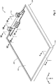
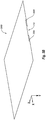
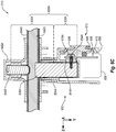
- Photovoltaiksystem (100), umfassend:mehrere Photovoltaikmodule (102, 200), wobei jedes Photovoltaikmodul (102, 200) ein erstes Ende (110, 202) und ein zweites Ende (112, 204) gegenüber dem ersten Ende (110, 202) definiert, wobei jedes Photovoltaikmodul (102, 200) Folgendes umfasst:mehrere Photovoltaikzellen (114, 404), wobei Energie, die durch jede Photovoltaikzelle (114, 404) erzeugt wird, mehrere Pfade durch die mehreren Photovoltaikzellen (114, 404) zum zweiten Ende (112, 204) aufweist; undmehrere Umsetzer (702), die elektrisch mit den mehreren Photovoltaikzellen (114, 404) am zweiten Ende (112, 204) gekoppelt sind, so dass Energie, die durch jede Photovoltaikzelle (114, 404) erzeugt wird, an einem beliebigen der mehreren Umsetzer (702) empfangen werden kann;eine durchgehende Rückwand (206, 206A, 206B), wobei die durchgehende Rückwand (206, 206A, 206B) eine Grundplatte für die mehreren Photovoltaikzellen (114, 404) umfasst;wobei die durchgehende Rückwand (206, 206A, 206B) elektrisch zwischen einer ersten Teilmenge (416) der mehreren Photovoltaikzellen (114, 404) am ersten Ende (110, 202) und einer zweiten Teilmenge (506) der mehreren Photovoltaikzellen (114, 404) am zweiten Ende (112, 204) gekoppelt ist, wobei die durchgehende Rückwand (206, 206A, 206B) dazu konfiguriert ist, einen Modulrückstrom vom zweiten Ende (112, 204) zum ersten Ende (110, 202) zu führen;eine erste Endverbindung (418, 412A) zwischen der durchgehenden Rückwand (206, 206A, 206B) und der ersten Teilmenge (416) der mehreren Photovoltaikzellen (114, 404) am ersten Ende (110, 202);eine zweite Endverbindung (412B, 508) zwischen den mehreren Umsetzern (702) und der zweiten Teilmenge (506) der mehreren Photovoltaikzellen (114, 404) am zweiten Ende (112, 204);eine Schaltungskarte (610), die mechanisch mit dem zweiten Ende (112, 204) gekoppelt ist, wobei die Schaltungskarte (610) die mehreren Umsetzer (702) darauf angeordnet beinhaltet und ferner einen positiven Anschluss (706) und einen negativen Anschluss (708) beinhaltet;einen internen Busstreifen (508), der sich entlang einer Breite des Photovoltaikmoduls (102, 200) erstreckt, wobei der interne Busstreifen (508) mit jeder der Photovoltaikzellen (114, 404) in der zweiten Teilmenge (506) der mehreren Photovoltaikzellen (114, 404) gekoppelt ist; undeinen Modul-Modul-Bus (104), der elektrisch mit jedem der mehreren Photovoltaikmodule (102, 200) gekoppelt ist, wobei der Modul-Modul-Bus (104) einen Ausgang aufweist, wobei Energie, die durch jedes Photovoltaikmodul (102, 200) erzeugt wird, unabhängig von einem jeglichen anderen der mehreren Photovoltaikmodule (102, 200) am Ausgang empfangen werden kann,wobei sich ein oder mehrere Abgriffe (306A, 306B, 308A, 308B) von der durchgehenden Rückwand (206, 206A, 206B) zu einem der Anschlüsse (706, 708) der Schaltungskarte (610) erstreckt bzw. erstrecken, wobei der eine oder die mehreren Abgriffe (306A, 306B, 308A, 308B) die durchgehende Rückwand (206, 206A, 206B) elektrisch mit dem einen der Anschlüsse (706, 708) der Schaltungskarte (610) koppelt bzw. koppeln,dadurch gekennzeichnet, dassder interne Busstreifen (508) einen Abgriff (508A) beinhaltet, der sich vom internen Busstreifen (508) durch einen Schlitz (304) oder einen Ausschnitt (310), der in der durchgehenden Rückwand (206, 206A, 206B) ausgebildet ist, zum anderen der Anschlüsse (706, 708) der Schaltungskarte (610) erstreckt, wobei der Abgriff (508A) den internen Busstreifen (508) elektrisch mit dem einen der Anschlüsse (706, 708) der Schaltungskarte (610) koppelt.
- Photovoltaiksystem (100) nach Anspruch 1, wobei jedes der mehreren Photovoltaikmodule (102, 200) ferner Folgendes umfasst:eine digitale Steuerung (704), die auf der Schaltungskarte (610) angeordnet ist;wobei die mehreren Umsetzer (702) jeweils unabhängig voneinander durch die digitale Steuerung (704) über gekoppelte Freigabe- und Pulsweitenmodulations(PWM)-Leitungen 724 von der digitalen Steuerung (704) zu jedem der mehreren Umsetzer (702) gesteuert werden; undwobei die digitale Steuerung (704) von jedem der Photovoltaikmodule (102, 200) zu Folgendem konfiguriert ist:langsames Laden von Strom auf den Modul-Modul-Bus (104), wenn eine Spannung auf dem Modul-Modul-Bus (104) geringer als eine Minimalschwelle (806) ist, um zu bestimmen, ob ein kapazitives Element am Modul-Modul-Bus (104) angebracht ist;als Reaktion auf das Bestimmen, dass ein kapazitives Element am Modul-Modul-Bus (104) angebracht ist, Fortfahren, Strom langsam auf den Modul-Modul-Bus (104) zu laden, bis die Spannung auf dem Modul-Modul-Bus (104) über die Minimalschwelle (806) ansteigt;Schließen eines Schutzrelais (716), wenn die Spannung auf dem Modul-Modul-Bus (104) über die Minimalschwelle (806) ansteigt, so dass eine Nullstromschaltung gewährleistet wird, wobei das Schutzrelais (716) elektrisch zwischen dem Modul-Modul-Bus (104) und einem Ausgangsbus (726) der Schaltungskarte (610) gekoppelt ist, wobei der Ausgangsbus (726) elektrisch mit Ausgängen (914) von jedem der mehreren Umsetzer (702) gekoppelt ist;Betreiben der mehreren Umsetzer (702) in einem Maximalstrommodus, wenn die Spannung auf dem Modul-Modul-Bus (104) zwischen der Minimalschwelle (806) und einer Zwischenschwelle (808), die größer als die Minimalschwelle (806) ist, liegt;Betreiben der mehreren Umsetzer (702) in einem Modus mit konstanter Spannung, wenn die Spannung auf dem Modul-Modul-Bus (104) zwischen der Zwischenschwelle (808) und einer Maximalschwelle (804), die größer als die Minimalschwelle (806) ist, liegt; undÖffnen des Schutzrelais (716), wenn die Spannung auf dem Modul-Modul-Bus (104) über die Maximalschwelle (804) ansteigt oder unter die Minimalschwelle (806) fällt.
- Photovoltaiksystem (100) nach Anspruch 1, wobei:die mehreren Photovoltaikzellen (114, 404) in mehreren Reihen (416, 506), die elektrisch in Reihe gekoppelt sind, angeordnet sind;jedes der mehreren Photovoltaikmodule (102, 200) ferner mehrere leitfähige Reihenstreifen (414) umfasst, die die Photovoltaikzellen (114, 404) in jeder Reihe (416, 506) elektrisch parallel miteinander koppeln; unddie mehreren Pfade durch die mehreren Photovoltaikzellen (114, 404) zum zweiten Ende (112, 204) die mehreren leitfähigen Reihenstreifen (414) beinhalten, so dass ein erzeugter Strom über die mehreren leitfähigen Reihenstreifen (414) um Photovoltaikzellen (114, 404) herum mit niedriger Leistung und/oder niedriger Illumination und durch Photovoltaikzellen (114, 404) mit relativ hoher Leistung und/oder hoher Illumination zum zweiten Ende (112, 204) fließen kann.
- Photovoltaiksystem (100) nach Anspruch 1, wobei:die erste Endverbindung (418, 412A) zwischen der durchgehenden Rückwand (206, 206A, 206B) und der ersten Teilmenge (416) der mehreren Photovoltaikzellen (114, 404) am ersten Ende (110, 202) eine Anode des Photovoltaikmoduls (102, 200) umfasst;die zweite Endverbindung (412B, 508) zwischen den mehreren Umsetzern (702) und der zweiten Teilmenge (506) der mehreren Photovoltaikzellen (114, 404) am zweiten Ende (112, 204) eine Kathode des Photovoltaikmoduls (102, 200) umfasst unddie durchgehende Rückwand (206, 206A, 206B) dazu konfiguriert ist, einen Modulrückstrom von der Kathode zur Anode zu führen.
- Photovoltaiksystem (100) nach Anspruch 4, wobei
der interne Busstreifen (508) mit einer Kathode von jeder der Photovoltaikzellen (114, 404) in der zweiten Teilmenge (506) der mehreren Photovoltaikzellen (114, 404) gekoppelt ist; und der Abgriff (508A) des internen Busstreifens (508) den internen Busstreifen (508) elektrisch mit dem positiven Anschluss (706) der Schaltungskarte (610) koppelt; und
wobei sich der eine oder die mehreren Abgriffe (306A, 306B, 308A, 308B) von der durchgehenden Rückwand (206, 206A, 206B) zum negativen Anschluss (708) der Schaltungskarte (610) erstreckt bzw. erstrecken, wobei der eine oder die mehreren Abgriffe (306A, 306B, 308A, 308B) die durchgehende Rückwand (206, 206A, 206B) elektrisch mit dem negativen Anschluss (708) der Schaltungskarte (610) koppelt bzw. koppeln. - Photovoltaiksystem (100) nach Anspruch 2, wobei jedes der mehreren Photovoltaikmodule (102, 200) ferner eine optische Signalquelle (728) beinhaltet, die kommunikativ mit der digitalen Steuerung (704) gekoppelt ist und so an der Schaltungskarte (610) befestigt ist, dass die durch die optische Signalquelle (728) emittierten optischen Signale von einer Vorderseite des entsprechenden Photovoltaikmoduls (102, 200) sichtbar sind.
- Photovoltaiksystem (100) nach Anspruch 2, wobei jedes der mehreren Photovoltaikmodule (102, 200) ferner eine Hochfrequenz (HF) emittierende Einrichtung (720) umfasst, die kommunikativ mit der digitalen Steuerung (704) gekoppelt ist, wobei die digitale Steuerung (704) dazu konfiguriert ist, die HF emittierende Einrichtung (720) zum Übermitteln von Informationen zu anderen der mehreren Photovoltaikmodule (102, 200) und/oder zu einer Datenerfassungseinrichtung, die im Photovoltaiksystem (100) enthalten ist, zu betreiben.
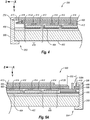
- Photovoltaiksystem (100) nach Anspruch 2, wobei jedes der mehreren Photovoltaikmodule (102, 200) ferner eine Unterbaubaugruppe (210) umfasst, in der die Schaltungskarte (610) angeordnet ist, wobei die Unterbaubaugruppe (210) ein Gehäuse (602) beinhaltet, das Folgendes umfasst:einen Hauptkörper (618) undmehrere Füße (620A-620C), die sich vom Hauptkörper (618) erstrecken, wobei die mehreren Füße (620A-620C) im Wesentlichen koplanar sind,wobei:die Unterbaubaugruppe (210) mechanisch mit der durchgehenden Rückwand (206, 206A, 206B) des entsprechenden Photovoltaikmoduls (102, 200) unter Verwendung eines Klebstoffs oder eines Klebebands (626), der bzw. das zwischen der durchgehenden Rückwand (206, 206A, 206B) und den mehreren Füßen (620A-620C) angeordnet ist, gekoppelt ist; undder Hauptkörper (618) zwei Schlitze (622A, 622B) definiert, durch die zwei entsprechende Steiger (606A, 606B) durch den Hauptkörper (618) laufen, um elektrisch mit der Schaltungskarte (610) gekoppelt zu werden.
- Photovoltaiksystem (100) nach Anspruch 1, wobei jeder der mehreren Umsetzer (702) mit einem Tastverhältnis D in einem Bereich von [(V_out - V_in) / V_out - 0,05] < D < 0,75 betrieben wird, wobei V_out und V_in eine Ausgangsspannung und eine Eingangsspannung des entsprechenden Umsetzers (702) sind.
- Photovoltaiksystem (100) nach Anspruch 1, wobei jedes der mehreren Photovoltaikmodule (102, 200) ferner Folgendes umfasst:Messschaltkreise (714), die dazu konfiguriert sind, einen Ausgangsstrom zum Modul-Modul-Bus (104) oder einen Eingangsstrom vom Modul-Modul-Bus (104) zu messen; undeine digitale Steuerung (704), die basierend auf der Messung dazu konfiguriert ist, einen Offset zwischen dem Ausgangsstrom und dem Eingangsstrom zu überwachen und/oder den Ausgangsstrom zu begrenzen, wenn der Ausgangsstrom eine voreingestellte Grenze überschreitet.
- Photovoltaiksystem (100) nach Anspruch 1, ferner umfassend:mehrere Wechselrichter (106), die elektrisch mit dem Modul-Modul-Bus (104) gekoppelt sind, so dass Energie, die durch jedes Photovoltaikmodul (102, 200) erzeugt wird, an einem beliebigen der mehreren Wechselrichter (106) empfangen werden kann.
- Photovoltaiksystem (100) nach Anspruch 11, wobei eine oder mehrere Energiespeichereinrichtungen (108) parallel mit dem Modul-Modul-Bus (104) gekoppelt sind.
- Photovoltaiksystem (100) nach Anspruch 12, wobei, basierend auf einem Gleichstromsollwert und einer Wechselstrombeschränkung von jedem der mehreren Wechselrichter (106) und basierend auf einem gegenwärtigen Ladezustand der einen oder der mehreren Energiespeichereinrichtungen (108), ein Strom folgendermaßen durch den Modul-Modul-Bus (104) und einen oder mehrere der mehreren Wechselrichter (106) fließt:in die eine oder die mehreren Energiespeichereinrichtungen (108) von einer beliebigen oder allen Phasen eines Mehrphasen-Wechselstrom-Energieversorgungsnetzes (118), mit dem jeder der mehreren Wechselrichter (106) gekoppelt ist; odervon der einen oder den mehreren Energiespeichereinrichtungen (108) in eine beliebige oder alle Phasen des Mehrphasen-Wechselstrom-Energieversorgungsnetzes (118).
- Photovoltaiksystem (100) nach Anspruch 11, wobei jeder der mehreren Wechselrichter (106) dazu konfiguriert ist, ferner mit einer beliebigen oder allen drei Phasen eines Dreiphasen-Wechselstrom-Energieversorgungsnetzes (118) gekoppelt zu werden.
- Photovoltaiksystem (100) nach Anspruch 11, wobei:die mehreren Wechselrichter (106) drei Wechselrichter (106) umfassen;jeder der drei Wechselrichter (106) ferner unter Verwendung einer Stern- oder Dreieckschaltung mit einer unterschiedlichen Phase eines Dreiphasen-Wechselstrom-Energieversorgungsnetzes (118) gekoppelt ist; undjeder der drei Wechselrichter (106) einen unterschiedlichen Gleichstromsollwert aufweist, so dass ein Strom während des Betriebs folgendermaßen fließt:von einer oder mehreren Phasen des Dreiphasen-Wechselstrom-Energieversorgungsnetzes (118) durch einen oder mehrere der mehreren Wechselrichter (106) mit einem relativ hohen Gleichstromsollwert zum Modul-Modul-Bus (104); undvom Modul-Modul-Bus (104) durch einen oder mehrere der mehreren Wechselrichter (106) mit einem relativ niedrigen Gleichstromsollwert zu einer oder mehreren anderen Phasen des Dreiphasen-Wechselstrom-Energieversorgungsnetzes (118).
Applications Claiming Priority (9)
| Application Number | Priority Date | Filing Date | Title |
|---|---|---|---|
| US201161553822P | 2011-10-31 | 2011-10-31 | |
| US201161554710P | 2011-11-02 | 2011-11-02 | |
| US201261585720P | 2012-01-12 | 2012-01-12 | |
| US201261590925P | 2012-01-26 | 2012-01-26 | |
| US201261620566P | 2012-04-05 | 2012-04-05 | |
| US201261694559P | 2012-08-29 | 2012-08-29 | |
| US201261694548P | 2012-08-29 | 2012-08-29 | |
| US201261699701P | 2012-09-11 | 2012-09-11 | |
| PCT/US2012/062784 WO2013066998A1 (en) | 2011-10-31 | 2012-10-31 | Cell-to-grid redundant photovoltaic system |
Publications (3)
| Publication Number | Publication Date |
|---|---|
| EP2774263A1 EP2774263A1 (de) | 2014-09-10 |
| EP2774263A4 EP2774263A4 (de) | 2015-01-21 |
| EP2774263B1 true EP2774263B1 (de) | 2017-10-18 |
Family
ID=48192710
Family Applications (1)
| Application Number | Title | Priority Date | Filing Date |
|---|---|---|---|
| EP12846494.8A Active EP2774263B1 (de) | 2011-10-31 | 2012-10-31 | Redundante zelle-zu-netz-fotovoltaikanlage |
Country Status (5)
| Country | Link |
|---|---|
| EP (1) | EP2774263B1 (de) |
| JP (2) | JP5956596B2 (de) |
| KR (1) | KR101602800B1 (de) |
| CN (1) | CN103999354B (de) |
| WO (1) | WO2013066998A1 (de) |
Families Citing this family (4)
| Publication number | Priority date | Publication date | Assignee | Title |
|---|---|---|---|---|
| EP3036829A4 (de) * | 2013-08-21 | 2017-08-09 | Tenksolar, Inc. | Vollständig redundante fotovoltaikanordnung |
| WO2016085987A1 (en) * | 2014-11-26 | 2016-06-02 | Visolis, Inc. | Processes for conversion of biologically derived mevalonic acid |
| KR102349774B1 (ko) * | 2015-03-11 | 2022-01-10 | 삼성전자주식회사 | 광전 회로 |
| US9312701B1 (en) * | 2015-07-16 | 2016-04-12 | Wi-Charge Ltd | System for optical wireless power supply |
Family Cites Families (25)
| Publication number | Priority date | Publication date | Assignee | Title |
|---|---|---|---|---|
| JPH1069321A (ja) * | 1996-08-27 | 1998-03-10 | Honda Motor Co Ltd | 太陽光発電装置 |
| JP2000357812A (ja) * | 1999-04-15 | 2000-12-26 | Canon Inc | 太陽電池モジュール及び発電装置 |
| JP2000358330A (ja) * | 1999-06-14 | 2000-12-26 | Nissin Electric Co Ltd | 太陽光発電装置 |
| AU773471B2 (en) * | 2000-10-20 | 2004-05-27 | Sphelar Power Corporation | Light-emitting or light-detecting semiconductor module and method of manufacture thereof |
| JP2004241753A (ja) * | 2002-12-13 | 2004-08-26 | Canon Inc | 太陽電池モジュール |
| JP4728687B2 (ja) * | 2005-04-22 | 2011-07-20 | 日本電信電話株式会社 | 昇圧装置 |
| CN1929235A (zh) * | 2005-09-09 | 2007-03-14 | 郝万福 | 智能电容式太阳能电源 |
| US20070095384A1 (en) * | 2005-10-28 | 2007-05-03 | Farquhar Donald S | Photovoltaic modules and interconnect methodology for fabricating the same |
| DE102006003904A1 (de) * | 2006-01-27 | 2007-08-09 | Sma Technologie Ag | Verfahren zur Umwandlung einer Gleichspannung in eine dreiphasige Wechselspannung |
| US20090217965A1 (en) * | 2006-04-21 | 2009-09-03 | Dougal Roger A | Apparatus and method for enhanced solar power generation and maximum power point tracking |
| US7900361B2 (en) * | 2006-12-06 | 2011-03-08 | Solaredge, Ltd. | Current bypass for distributed power harvesting systems using DC power sources |
| JP4987608B2 (ja) * | 2007-07-27 | 2012-07-25 | シャープ株式会社 | 太陽光発電システム |
| US8138631B2 (en) * | 2007-12-21 | 2012-03-20 | Eiq Energy, Inc. | Advanced renewable energy harvesting |
| US8933320B2 (en) | 2008-01-18 | 2015-01-13 | Tenksolar, Inc. | Redundant electrical architecture for photovoltaic modules |
| TWI384720B (zh) * | 2008-07-17 | 2013-02-01 | Atomic Energy Council | 家用負載之直流電力裝置 |
| US8115340B2 (en) * | 2008-12-12 | 2012-02-14 | Paceco Corp. | System for controlling power from a photovoltaic array by selectively configurating connections between photovoltaic panels |
| JP5301685B2 (ja) * | 2009-02-23 | 2013-09-25 | テンケーソーラー インコーポレイテッド | 高効率再生可能な太陽エネルギシステム |
| WO2010114995A1 (en) * | 2009-04-01 | 2010-10-07 | Nextronex Energy Systems, Llc | A grid tie solar system and a method |
| JP4673921B2 (ja) * | 2009-05-01 | 2011-04-20 | オーナンバ株式会社 | 太陽電池発電システムの異常検出装置及び方法 |
| EP2911263A3 (de) * | 2009-06-15 | 2015-10-14 | Tenksolar, Inc. | Beleuchtungsagnostische solartafel |
| JP5402289B2 (ja) * | 2009-06-18 | 2014-01-29 | 日産自動車株式会社 | 電力供給装置 |
| US20110018353A1 (en) * | 2009-07-23 | 2011-01-27 | Wenjiang Yu | Method and apparatus for multi-source electrical energy grid-tied transformation |
| EP2280469B1 (de) * | 2009-07-30 | 2016-07-06 | Nxp B.V. | Photovoltaische Einheit, Gleichstromwandler dafür und Verfahren zu deren Betrieb |
| CN102484372B (zh) * | 2009-08-24 | 2014-06-18 | 三菱电机株式会社 | 太阳能发电用功率调节器 |
| CN101800498B (zh) * | 2010-04-01 | 2013-12-04 | 华为技术有限公司 | 太阳能光发电系统、控制装置及控制方法 |
-
2012
- 2012-10-31 JP JP2014540038A patent/JP5956596B2/ja active Active
- 2012-10-31 KR KR1020147014579A patent/KR101602800B1/ko active IP Right Grant
- 2012-10-31 WO PCT/US2012/062784 patent/WO2013066998A1/en active Application Filing
- 2012-10-31 CN CN201280057171.7A patent/CN103999354B/zh active Active
- 2012-10-31 EP EP12846494.8A patent/EP2774263B1/de active Active
-
2016
- 2016-06-16 JP JP2016119739A patent/JP2016201548A/ja active Pending
Non-Patent Citations (1)
| Title |
|---|
| None * |
Also Published As
| Publication number | Publication date |
|---|---|
| KR101602800B1 (ko) | 2016-03-11 |
| KR20140117354A (ko) | 2014-10-07 |
| EP2774263A1 (de) | 2014-09-10 |
| WO2013066998A1 (en) | 2013-05-10 |
| EP2774263A4 (de) | 2015-01-21 |
| JP2015502728A (ja) | 2015-01-22 |
| CN103999354A (zh) | 2014-08-20 |
| CN103999354B (zh) | 2017-03-01 |
| JP5956596B2 (ja) | 2016-07-27 |
| JP2016201548A (ja) | 2016-12-01 |
Similar Documents
| Publication | Publication Date | Title |
|---|---|---|
| US9299861B2 (en) | Cell-to-grid redundandt photovoltaic system | |
| US9768725B2 (en) | Redundant electrical architecture for photovoltaic modules | |
| JP5966027B2 (ja) | 不均一な照度に寛容な太陽電池パネルのための光起電力モジュールの電力制御方法 | |
| US10277165B2 (en) | Photovoltaic module | |
| US8748727B2 (en) | Flat-plate photovoltaic module | |
| KR100550694B1 (ko) | 발전시스템 및 발전장치 | |
| US20160301360A1 (en) | Photovoltaic module | |
| JP5792742B2 (ja) | 発電のための太陽光システム | |
| JP2000315808A (ja) | 太陽電池を備えた電力発生のための回路装置 | |
| EP2774263B1 (de) | Redundante zelle-zu-netz-fotovoltaikanlage | |
| EP3297117A1 (de) | Verteiltes stromsystem, gleichspannungswandler und power conditioner | |
| WO2009092111A2 (en) | Flat-plate photovoltaic module | |
| WO2009092110A2 (en) | Redundant electrical architecture for photovoltaic modules | |
| KR101788013B1 (ko) | 태양광 모듈 | |
| JP2013033832A (ja) | 太陽電池モジュール | |
| CN215933780U (zh) | 电池模组及电池包 |
Legal Events
| Date | Code | Title | Description |
|---|---|---|---|
| PUAI | Public reference made under article 153(3) epc to a published international application that has entered the european phase |
Free format text: ORIGINAL CODE: 0009012 |
|
| 17P | Request for examination filed |
Effective date: 20140522 |
|
| AK | Designated contracting states |
Kind code of ref document: A1 Designated state(s): AL AT BE BG CH CY CZ DE DK EE ES FI FR GB GR HR HU IE IS IT LI LT LU LV MC MK MT NL NO PL PT RO RS SE SI SK SM TR |
|
| RIN1 | Information on inventor provided before grant (corrected) |
Inventor name: NOVOTNY, JOHN Inventor name: GROSS, SHADY Inventor name: MEYER, DALLAS, W. Inventor name: BERG, LOWELL Inventor name: MEYER, FORREST, C. |
|
| REG | Reference to a national code |
Ref country code: DE Ref legal event code: R079 Ref document number: 602012038781 Country of ref document: DE Free format text: PREVIOUS MAIN CLASS: H02N0006000000 Ipc: H02S0099000000 |
|
| A4 | Supplementary search report drawn up and despatched |
Effective date: 20141218 |
|
| RIC1 | Information provided on ipc code assigned before grant |
Ipc: H02S 99/00 20140101AFI20141218BHEP Ipc: H01L 31/042 20140101ALI20141218BHEP |
|
| DAX | Request for extension of the european patent (deleted) | ||
| 17Q | First examination report despatched |
Effective date: 20151016 |
|
| GRAP | Despatch of communication of intention to grant a patent |
Free format text: ORIGINAL CODE: EPIDOSNIGR1 |
|
| INTG | Intention to grant announced |
Effective date: 20170516 |
|
| GRAS | Grant fee paid |
Free format text: ORIGINAL CODE: EPIDOSNIGR3 |
|
| GRAA | (expected) grant |
Free format text: ORIGINAL CODE: 0009210 |
|
| AK | Designated contracting states |
Kind code of ref document: B1 Designated state(s): AL AT BE BG CH CY CZ DE DK EE ES FI FR GB GR HR HU IE IS IT LI LT LU LV MC MK MT NL NO PL PT RO RS SE SI SK SM TR |
|
| REG | Reference to a national code |
Ref country code: GB Ref legal event code: FG4D |
|
| REG | Reference to a national code |
Ref country code: CH Ref legal event code: EP |
|
| REG | Reference to a national code |
Ref country code: AT Ref legal event code: REF Ref document number: 938758 Country of ref document: AT Kind code of ref document: T Effective date: 20171115 Ref country code: IE Ref legal event code: FG4D |
|
| REG | Reference to a national code |
Ref country code: DE Ref legal event code: R096 Ref document number: 602012038781 Country of ref document: DE |
|
| REG | Reference to a national code |
Ref country code: FR Ref legal event code: PLFP Year of fee payment: 6 |
|
| REG | Reference to a national code |
Ref country code: NL Ref legal event code: MP Effective date: 20171018 |
|
| REG | Reference to a national code |
Ref country code: LT Ref legal event code: MG4D |
|
| REG | Reference to a national code |
Ref country code: AT Ref legal event code: MK05 Ref document number: 938758 Country of ref document: AT Kind code of ref document: T Effective date: 20171018 |
|
| PG25 | Lapsed in a contracting state [announced via postgrant information from national office to epo] |
Ref country code: NL Free format text: LAPSE BECAUSE OF FAILURE TO SUBMIT A TRANSLATION OF THE DESCRIPTION OR TO PAY THE FEE WITHIN THE PRESCRIBED TIME-LIMIT Effective date: 20171018 |
|
| PG25 | Lapsed in a contracting state [announced via postgrant information from national office to epo] |
Ref country code: ES Free format text: LAPSE BECAUSE OF FAILURE TO SUBMIT A TRANSLATION OF THE DESCRIPTION OR TO PAY THE FEE WITHIN THE PRESCRIBED TIME-LIMIT Effective date: 20171018 Ref country code: LT Free format text: LAPSE BECAUSE OF FAILURE TO SUBMIT A TRANSLATION OF THE DESCRIPTION OR TO PAY THE FEE WITHIN THE PRESCRIBED TIME-LIMIT Effective date: 20171018 Ref country code: SE Free format text: LAPSE BECAUSE OF FAILURE TO SUBMIT A TRANSLATION OF THE DESCRIPTION OR TO PAY THE FEE WITHIN THE PRESCRIBED TIME-LIMIT Effective date: 20171018 Ref country code: NO Free format text: LAPSE BECAUSE OF FAILURE TO SUBMIT A TRANSLATION OF THE DESCRIPTION OR TO PAY THE FEE WITHIN THE PRESCRIBED TIME-LIMIT Effective date: 20180118 Ref country code: FI Free format text: LAPSE BECAUSE OF FAILURE TO SUBMIT A TRANSLATION OF THE DESCRIPTION OR TO PAY THE FEE WITHIN THE PRESCRIBED TIME-LIMIT Effective date: 20171018 |
|
| PG25 | Lapsed in a contracting state [announced via postgrant information from national office to epo] |
Ref country code: BG Free format text: LAPSE BECAUSE OF FAILURE TO SUBMIT A TRANSLATION OF THE DESCRIPTION OR TO PAY THE FEE WITHIN THE PRESCRIBED TIME-LIMIT Effective date: 20180118 Ref country code: IS Free format text: LAPSE BECAUSE OF FAILURE TO SUBMIT A TRANSLATION OF THE DESCRIPTION OR TO PAY THE FEE WITHIN THE PRESCRIBED TIME-LIMIT Effective date: 20180218 Ref country code: HR Free format text: LAPSE BECAUSE OF FAILURE TO SUBMIT A TRANSLATION OF THE DESCRIPTION OR TO PAY THE FEE WITHIN THE PRESCRIBED TIME-LIMIT Effective date: 20171018 Ref country code: LV Free format text: LAPSE BECAUSE OF FAILURE TO SUBMIT A TRANSLATION OF THE DESCRIPTION OR TO PAY THE FEE WITHIN THE PRESCRIBED TIME-LIMIT Effective date: 20171018 Ref country code: GR Free format text: LAPSE BECAUSE OF FAILURE TO SUBMIT A TRANSLATION OF THE DESCRIPTION OR TO PAY THE FEE WITHIN THE PRESCRIBED TIME-LIMIT Effective date: 20180119 Ref country code: AT Free format text: LAPSE BECAUSE OF FAILURE TO SUBMIT A TRANSLATION OF THE DESCRIPTION OR TO PAY THE FEE WITHIN THE PRESCRIBED TIME-LIMIT Effective date: 20171018 Ref country code: RS Free format text: LAPSE BECAUSE OF FAILURE TO SUBMIT A TRANSLATION OF THE DESCRIPTION OR TO PAY THE FEE WITHIN THE PRESCRIBED TIME-LIMIT Effective date: 20171018 |
|
| REG | Reference to a national code |
Ref country code: CH Ref legal event code: PL |
|
| REG | Reference to a national code |
Ref country code: DE Ref legal event code: R097 Ref document number: 602012038781 Country of ref document: DE |
|
| REG | Reference to a national code |
Ref country code: IE Ref legal event code: MM4A |
|
| PG25 | Lapsed in a contracting state [announced via postgrant information from national office to epo] |
Ref country code: DK Free format text: LAPSE BECAUSE OF FAILURE TO SUBMIT A TRANSLATION OF THE DESCRIPTION OR TO PAY THE FEE WITHIN THE PRESCRIBED TIME-LIMIT Effective date: 20171018 Ref country code: EE Free format text: LAPSE BECAUSE OF FAILURE TO SUBMIT A TRANSLATION OF THE DESCRIPTION OR TO PAY THE FEE WITHIN THE PRESCRIBED TIME-LIMIT Effective date: 20171018 Ref country code: LU Free format text: LAPSE BECAUSE OF NON-PAYMENT OF DUE FEES Effective date: 20171031 Ref country code: MC Free format text: LAPSE BECAUSE OF FAILURE TO SUBMIT A TRANSLATION OF THE DESCRIPTION OR TO PAY THE FEE WITHIN THE PRESCRIBED TIME-LIMIT Effective date: 20171018 Ref country code: SK Free format text: LAPSE BECAUSE OF FAILURE TO SUBMIT A TRANSLATION OF THE DESCRIPTION OR TO PAY THE FEE WITHIN THE PRESCRIBED TIME-LIMIT Effective date: 20171018 Ref country code: LI Free format text: LAPSE BECAUSE OF NON-PAYMENT OF DUE FEES Effective date: 20171031 Ref country code: CH Free format text: LAPSE BECAUSE OF NON-PAYMENT OF DUE FEES Effective date: 20171031 Ref country code: CZ Free format text: LAPSE BECAUSE OF FAILURE TO SUBMIT A TRANSLATION OF THE DESCRIPTION OR TO PAY THE FEE WITHIN THE PRESCRIBED TIME-LIMIT Effective date: 20171018 |
|
| REG | Reference to a national code |
Ref country code: BE Ref legal event code: MM Effective date: 20171031 |
|
| PLBE | No opposition filed within time limit |
Free format text: ORIGINAL CODE: 0009261 |
|
| STAA | Information on the status of an ep patent application or granted ep patent |
Free format text: STATUS: NO OPPOSITION FILED WITHIN TIME LIMIT |
|
| PG25 | Lapsed in a contracting state [announced via postgrant information from national office to epo] |
Ref country code: SM Free format text: LAPSE BECAUSE OF FAILURE TO SUBMIT A TRANSLATION OF THE DESCRIPTION OR TO PAY THE FEE WITHIN THE PRESCRIBED TIME-LIMIT Effective date: 20171018 Ref country code: BE Free format text: LAPSE BECAUSE OF NON-PAYMENT OF DUE FEES Effective date: 20171031 Ref country code: IT Free format text: LAPSE BECAUSE OF FAILURE TO SUBMIT A TRANSLATION OF THE DESCRIPTION OR TO PAY THE FEE WITHIN THE PRESCRIBED TIME-LIMIT Effective date: 20171018 Ref country code: RO Free format text: LAPSE BECAUSE OF FAILURE TO SUBMIT A TRANSLATION OF THE DESCRIPTION OR TO PAY THE FEE WITHIN THE PRESCRIBED TIME-LIMIT Effective date: 20171018 Ref country code: PL Free format text: LAPSE BECAUSE OF FAILURE TO SUBMIT A TRANSLATION OF THE DESCRIPTION OR TO PAY THE FEE WITHIN THE PRESCRIBED TIME-LIMIT Effective date: 20171018 |
|
| REG | Reference to a national code |
Ref country code: FR Ref legal event code: PLFP Year of fee payment: 7 |
|
| 26N | No opposition filed |
Effective date: 20180719 |
|
| PG25 | Lapsed in a contracting state [announced via postgrant information from national office to epo] |
Ref country code: MT Free format text: LAPSE BECAUSE OF NON-PAYMENT OF DUE FEES Effective date: 20171031 |
|
| PG25 | Lapsed in a contracting state [announced via postgrant information from national office to epo] |
Ref country code: IE Free format text: LAPSE BECAUSE OF NON-PAYMENT OF DUE FEES Effective date: 20171031 |
|
| PG25 | Lapsed in a contracting state [announced via postgrant information from national office to epo] |
Ref country code: SI Free format text: LAPSE BECAUSE OF FAILURE TO SUBMIT A TRANSLATION OF THE DESCRIPTION OR TO PAY THE FEE WITHIN THE PRESCRIBED TIME-LIMIT Effective date: 20171018 |
|
| PG25 | Lapsed in a contracting state [announced via postgrant information from national office to epo] |
Ref country code: HU Free format text: LAPSE BECAUSE OF FAILURE TO SUBMIT A TRANSLATION OF THE DESCRIPTION OR TO PAY THE FEE WITHIN THE PRESCRIBED TIME-LIMIT; INVALID AB INITIO Effective date: 20121031 |
|
| PG25 | Lapsed in a contracting state [announced via postgrant information from national office to epo] |
Ref country code: CY Free format text: LAPSE BECAUSE OF NON-PAYMENT OF DUE FEES Effective date: 20171018 |
|
| REG | Reference to a national code |
Ref country code: DE Ref legal event code: R082 Ref document number: 602012038781 Country of ref document: DE Representative=s name: KRAUS & LEDERER PARTGMBB, DE Ref country code: DE Ref legal event code: R082 Ref document number: 602012038781 Country of ref document: DE Representative=s name: KRAUS & WEISERT PATENTANWAELTE PARTGMBB, DE Ref country code: DE Ref legal event code: R081 Ref document number: 602012038781 Country of ref document: DE Owner name: SPECTRUM SOLAR, LLC, HUNSTVILLE, US Free format text: FORMER OWNER: TENKSOLAR, INC., MINNEAPOLIS, MINN., US |
|
| PG25 | Lapsed in a contracting state [announced via postgrant information from national office to epo] |
Ref country code: MK Free format text: LAPSE BECAUSE OF FAILURE TO SUBMIT A TRANSLATION OF THE DESCRIPTION OR TO PAY THE FEE WITHIN THE PRESCRIBED TIME-LIMIT Effective date: 20171018 |
|
| PG25 | Lapsed in a contracting state [announced via postgrant information from national office to epo] |
Ref country code: TR Free format text: LAPSE BECAUSE OF FAILURE TO SUBMIT A TRANSLATION OF THE DESCRIPTION OR TO PAY THE FEE WITHIN THE PRESCRIBED TIME-LIMIT Effective date: 20171018 |
|
| PG25 | Lapsed in a contracting state [announced via postgrant information from national office to epo] |
Ref country code: PT Free format text: LAPSE BECAUSE OF FAILURE TO SUBMIT A TRANSLATION OF THE DESCRIPTION OR TO PAY THE FEE WITHIN THE PRESCRIBED TIME-LIMIT Effective date: 20171018 |
|
| PG25 | Lapsed in a contracting state [announced via postgrant information from national office to epo] |
Ref country code: AL Free format text: LAPSE BECAUSE OF FAILURE TO SUBMIT A TRANSLATION OF THE DESCRIPTION OR TO PAY THE FEE WITHIN THE PRESCRIBED TIME-LIMIT Effective date: 20171018 |
|
| P01 | Opt-out of the competence of the unified patent court (upc) registered |
Effective date: 20230517 |
|
| PGFP | Annual fee paid to national office [announced via postgrant information from national office to epo] |
Ref country code: GB Payment date: 20231003 Year of fee payment: 12 |
|
| PGFP | Annual fee paid to national office [announced via postgrant information from national office to epo] |
Ref country code: FR Payment date: 20231004 Year of fee payment: 12 Ref country code: DE Payment date: 20231011 Year of fee payment: 12 |