EP2772802A1 - Fotolithografieverfahren mit Doppelmaske, bei dem die Auswirkung von Substratfehlern minimiert ist - Google Patents
Fotolithografieverfahren mit Doppelmaske, bei dem die Auswirkung von Substratfehlern minimiert ist Download PDFInfo
- Publication number
- EP2772802A1 EP2772802A1 EP14155467.5A EP14155467A EP2772802A1 EP 2772802 A1 EP2772802 A1 EP 2772802A1 EP 14155467 A EP14155467 A EP 14155467A EP 2772802 A1 EP2772802 A1 EP 2772802A1
- Authority
- EP
- European Patent Office
- Prior art keywords
- mask
- pattern
- defects
- mask blank
- blank
- Prior art date
- Legal status (The legal status is an assumption and is not a legal conclusion. Google has not performed a legal analysis and makes no representation as to the accuracy of the status listed.)
- Granted
Links
- 230000007547 defect Effects 0.000 title claims abstract description 75
- 238000000206 photolithography Methods 0.000 title claims abstract description 31
- 238000000034 method Methods 0.000 title claims abstract description 17
- 239000000758 substrate Substances 0.000 title description 8
- 230000007717 exclusion Effects 0.000 claims abstract description 54
- 238000013507 mapping Methods 0.000 claims abstract description 7
- 238000007689 inspection Methods 0.000 claims abstract description 6
- 230000000295 complement effect Effects 0.000 claims description 18
- 230000003287 optical effect Effects 0.000 claims description 5
- 238000012937 correction Methods 0.000 claims description 4
- 230000008569 process Effects 0.000 claims description 3
- 238000013461 design Methods 0.000 abstract description 14
- 230000002745 absorbent Effects 0.000 description 14
- 239000002250 absorbent Substances 0.000 description 14
- XUIMIQQOPSSXEZ-UHFFFAOYSA-N Silicon Chemical compound [Si] XUIMIQQOPSSXEZ-UHFFFAOYSA-N 0.000 description 6
- 241000209149 Zea Species 0.000 description 6
- 229910052710 silicon Inorganic materials 0.000 description 6
- 239000010703 silicon Substances 0.000 description 6
- 235000012431 wafers Nutrition 0.000 description 6
- 239000011347 resin Substances 0.000 description 5
- 229920005989 resin Polymers 0.000 description 5
- ZOKXTWBITQBERF-UHFFFAOYSA-N Molybdenum Chemical compound [Mo] ZOKXTWBITQBERF-UHFFFAOYSA-N 0.000 description 4
- 229910052750 molybdenum Inorganic materials 0.000 description 4
- 239000011733 molybdenum Substances 0.000 description 4
- 230000010363 phase shift Effects 0.000 description 4
- VYZAMTAEIAYCRO-UHFFFAOYSA-N Chromium Chemical compound [Cr] VYZAMTAEIAYCRO-UHFFFAOYSA-N 0.000 description 3
- 229910052804 chromium Inorganic materials 0.000 description 3
- 239000011651 chromium Substances 0.000 description 3
- 230000000694 effects Effects 0.000 description 3
- 238000004519 manufacturing process Methods 0.000 description 3
- 238000005192 partition Methods 0.000 description 3
- 239000004065 semiconductor Substances 0.000 description 3
- 240000008042 Zea mays Species 0.000 description 2
- 230000008901 benefit Effects 0.000 description 2
- 230000015572 biosynthetic process Effects 0.000 description 2
- 238000010894 electron beam technology Methods 0.000 description 2
- 238000002513 implantation Methods 0.000 description 2
- 230000000873 masking effect Effects 0.000 description 2
- 238000004377 microelectronic Methods 0.000 description 2
- 238000012986 modification Methods 0.000 description 2
- 230000004048 modification Effects 0.000 description 2
- 230000005855 radiation Effects 0.000 description 2
- VYPSYNLAJGMNEJ-UHFFFAOYSA-N Silicium dioxide Chemical compound O=[Si]=O VYPSYNLAJGMNEJ-UHFFFAOYSA-N 0.000 description 1
- 230000005540 biological transmission Effects 0.000 description 1
- 238000004364 calculation method Methods 0.000 description 1
- 238000012822 chemical development Methods 0.000 description 1
- 230000007812 deficiency Effects 0.000 description 1
- 230000002950 deficient Effects 0.000 description 1
- 230000002542 deteriorative effect Effects 0.000 description 1
- 238000005538 encapsulation Methods 0.000 description 1
- 238000005516 engineering process Methods 0.000 description 1
- 238000005530 etching Methods 0.000 description 1
- 238000005286 illumination Methods 0.000 description 1
- 239000007943 implant Substances 0.000 description 1
- 238000001459 lithography Methods 0.000 description 1
- 230000009467 reduction Effects 0.000 description 1
- 230000008439 repair process Effects 0.000 description 1
- 229910052814 silicon oxide Inorganic materials 0.000 description 1
- 238000004381 surface treatment Methods 0.000 description 1
- 239000010409 thin film Substances 0.000 description 1
- 238000013519 translation Methods 0.000 description 1
Images


Classifications
-
- G—PHYSICS
- G03—PHOTOGRAPHY; CINEMATOGRAPHY; ANALOGOUS TECHNIQUES USING WAVES OTHER THAN OPTICAL WAVES; ELECTROGRAPHY; HOLOGRAPHY
- G03F—PHOTOMECHANICAL PRODUCTION OF TEXTURED OR PATTERNED SURFACES, e.g. FOR PRINTING, FOR PROCESSING OF SEMICONDUCTOR DEVICES; MATERIALS THEREFOR; ORIGINALS THEREFOR; APPARATUS SPECIALLY ADAPTED THEREFOR
- G03F7/00—Photomechanical, e.g. photolithographic, production of textured or patterned surfaces, e.g. printing surfaces; Materials therefor, e.g. comprising photoresists; Apparatus specially adapted therefor
- G03F7/20—Exposure; Apparatus therefor
- G03F7/2022—Multi-step exposure, e.g. hybrid; backside exposure; blanket exposure, e.g. for image reversal; edge exposure, e.g. for edge bead removal; corrective exposure
- G03F7/2026—Multi-step exposure, e.g. hybrid; backside exposure; blanket exposure, e.g. for image reversal; edge exposure, e.g. for edge bead removal; corrective exposure for the removal of unwanted material, e.g. image or background correction
-
- H—ELECTRICITY
- H01—ELECTRIC ELEMENTS
- H01L—SEMICONDUCTOR DEVICES NOT COVERED BY CLASS H10
- H01L21/00—Processes or apparatus adapted for the manufacture or treatment of semiconductor or solid state devices or of parts thereof
- H01L21/02—Manufacture or treatment of semiconductor devices or of parts thereof
- H01L21/027—Making masks on semiconductor bodies for further photolithographic processing not provided for in group H01L21/18 or H01L21/34
- H01L21/0271—Making masks on semiconductor bodies for further photolithographic processing not provided for in group H01L21/18 or H01L21/34 comprising organic layers
- H01L21/0273—Making masks on semiconductor bodies for further photolithographic processing not provided for in group H01L21/18 or H01L21/34 comprising organic layers characterised by the treatment of photoresist layers
-
- G—PHYSICS
- G03—PHOTOGRAPHY; CINEMATOGRAPHY; ANALOGOUS TECHNIQUES USING WAVES OTHER THAN OPTICAL WAVES; ELECTROGRAPHY; HOLOGRAPHY
- G03F—PHOTOMECHANICAL PRODUCTION OF TEXTURED OR PATTERNED SURFACES, e.g. FOR PRINTING, FOR PROCESSING OF SEMICONDUCTOR DEVICES; MATERIALS THEREFOR; ORIGINALS THEREFOR; APPARATUS SPECIALLY ADAPTED THEREFOR
- G03F1/00—Originals for photomechanical production of textured or patterned surfaces, e.g., masks, photo-masks, reticles; Mask blanks or pellicles therefor; Containers specially adapted therefor; Preparation thereof
- G03F1/22—Masks or mask blanks for imaging by radiation of 100nm or shorter wavelength, e.g. X-ray masks, extreme ultraviolet [EUV] masks; Preparation thereof
- G03F1/24—Reflection masks; Preparation thereof
-
- G—PHYSICS
- G03—PHOTOGRAPHY; CINEMATOGRAPHY; ANALOGOUS TECHNIQUES USING WAVES OTHER THAN OPTICAL WAVES; ELECTROGRAPHY; HOLOGRAPHY
- G03F—PHOTOMECHANICAL PRODUCTION OF TEXTURED OR PATTERNED SURFACES, e.g. FOR PRINTING, FOR PROCESSING OF SEMICONDUCTOR DEVICES; MATERIALS THEREFOR; ORIGINALS THEREFOR; APPARATUS SPECIALLY ADAPTED THEREFOR
- G03F1/00—Originals for photomechanical production of textured or patterned surfaces, e.g., masks, photo-masks, reticles; Mask blanks or pellicles therefor; Containers specially adapted therefor; Preparation thereof
- G03F1/68—Preparation processes not covered by groups G03F1/20 - G03F1/50
- G03F1/70—Adapting basic layout or design of masks to lithographic process requirements, e.g., second iteration correction of mask patterns for imaging
-
- G—PHYSICS
- G03—PHOTOGRAPHY; CINEMATOGRAPHY; ANALOGOUS TECHNIQUES USING WAVES OTHER THAN OPTICAL WAVES; ELECTROGRAPHY; HOLOGRAPHY
- G03F—PHOTOMECHANICAL PRODUCTION OF TEXTURED OR PATTERNED SURFACES, e.g. FOR PRINTING, FOR PROCESSING OF SEMICONDUCTOR DEVICES; MATERIALS THEREFOR; ORIGINALS THEREFOR; APPARATUS SPECIALLY ADAPTED THEREFOR
- G03F1/00—Originals for photomechanical production of textured or patterned surfaces, e.g., masks, photo-masks, reticles; Mask blanks or pellicles therefor; Containers specially adapted therefor; Preparation thereof
- G03F1/68—Preparation processes not covered by groups G03F1/20 - G03F1/50
- G03F1/72—Repair or correction of mask defects
-
- G—PHYSICS
- G03—PHOTOGRAPHY; CINEMATOGRAPHY; ANALOGOUS TECHNIQUES USING WAVES OTHER THAN OPTICAL WAVES; ELECTROGRAPHY; HOLOGRAPHY
- G03F—PHOTOMECHANICAL PRODUCTION OF TEXTURED OR PATTERNED SURFACES, e.g. FOR PRINTING, FOR PROCESSING OF SEMICONDUCTOR DEVICES; MATERIALS THEREFOR; ORIGINALS THEREFOR; APPARATUS SPECIALLY ADAPTED THEREFOR
- G03F1/00—Originals for photomechanical production of textured or patterned surfaces, e.g., masks, photo-masks, reticles; Mask blanks or pellicles therefor; Containers specially adapted therefor; Preparation thereof
- G03F1/68—Preparation processes not covered by groups G03F1/20 - G03F1/50
- G03F1/82—Auxiliary processes, e.g. cleaning or inspecting
- G03F1/84—Inspecting
-
- G—PHYSICS
- G03—PHOTOGRAPHY; CINEMATOGRAPHY; ANALOGOUS TECHNIQUES USING WAVES OTHER THAN OPTICAL WAVES; ELECTROGRAPHY; HOLOGRAPHY
- G03F—PHOTOMECHANICAL PRODUCTION OF TEXTURED OR PATTERNED SURFACES, e.g. FOR PRINTING, FOR PROCESSING OF SEMICONDUCTOR DEVICES; MATERIALS THEREFOR; ORIGINALS THEREFOR; APPARATUS SPECIALLY ADAPTED THEREFOR
- G03F7/00—Photomechanical, e.g. photolithographic, production of textured or patterned surfaces, e.g. printing surfaces; Materials therefor, e.g. comprising photoresists; Apparatus specially adapted therefor
- G03F7/70—Microphotolithographic exposure; Apparatus therefor
- G03F7/70425—Imaging strategies, e.g. for increasing throughput or resolution, printing product fields larger than the image field or compensating lithography- or non-lithography errors, e.g. proximity correction, mix-and-match, stitching or double patterning
- G03F7/70433—Layout for increasing efficiency or for compensating imaging errors, e.g. layout of exposure fields for reducing focus errors; Use of mask features for increasing efficiency or for compensating imaging errors
-
- G—PHYSICS
- G03—PHOTOGRAPHY; CINEMATOGRAPHY; ANALOGOUS TECHNIQUES USING WAVES OTHER THAN OPTICAL WAVES; ELECTROGRAPHY; HOLOGRAPHY
- G03F—PHOTOMECHANICAL PRODUCTION OF TEXTURED OR PATTERNED SURFACES, e.g. FOR PRINTING, FOR PROCESSING OF SEMICONDUCTOR DEVICES; MATERIALS THEREFOR; ORIGINALS THEREFOR; APPARATUS SPECIALLY ADAPTED THEREFOR
- G03F7/00—Photomechanical, e.g. photolithographic, production of textured or patterned surfaces, e.g. printing surfaces; Materials therefor, e.g. comprising photoresists; Apparatus specially adapted therefor
- G03F7/70—Microphotolithographic exposure; Apparatus therefor
- G03F7/70425—Imaging strategies, e.g. for increasing throughput or resolution, printing product fields larger than the image field or compensating lithography- or non-lithography errors, e.g. proximity correction, mix-and-match, stitching or double patterning
- G03F7/70466—Multiple exposures, e.g. combination of fine and coarse exposures, double patterning or multiple exposures for printing a single feature
-
- G—PHYSICS
- G03—PHOTOGRAPHY; CINEMATOGRAPHY; ANALOGOUS TECHNIQUES USING WAVES OTHER THAN OPTICAL WAVES; ELECTROGRAPHY; HOLOGRAPHY
- G03F—PHOTOMECHANICAL PRODUCTION OF TEXTURED OR PATTERNED SURFACES, e.g. FOR PRINTING, FOR PROCESSING OF SEMICONDUCTOR DEVICES; MATERIALS THEREFOR; ORIGINALS THEREFOR; APPARATUS SPECIALLY ADAPTED THEREFOR
- G03F7/00—Photomechanical, e.g. photolithographic, production of textured or patterned surfaces, e.g. printing surfaces; Materials therefor, e.g. comprising photoresists; Apparatus specially adapted therefor
- G03F7/70—Microphotolithographic exposure; Apparatus therefor
- G03F7/70483—Information management; Active and passive control; Testing; Wafer monitoring, e.g. pattern monitoring
- G03F7/70605—Workpiece metrology
- G03F7/70616—Monitoring the printed patterns
- G03F7/7065—Defects, e.g. optical inspection of patterned layer for defects
-
- G—PHYSICS
- G06—COMPUTING; CALCULATING OR COUNTING
- G06F—ELECTRIC DIGITAL DATA PROCESSING
- G06F2119/00—Details relating to the type or aim of the analysis or the optimisation
- G06F2119/18—Manufacturability analysis or optimisation for manufacturability
Definitions
- the invention relates to the manufacture of photolithography masks.
- Ultraviolet photolithography EUV
- the wavelengths considered are less than 20 nanometers and are typically 13.5 nm or 6.8 nm.
- the use of these wavelengths is intended to produce patterns of smaller dimensions than those allowed by photolithography in visible light or in deep ultraviolet (DUV), but the invention applies to any length of light. 'wave.
- EUV masks are used in reflection and not in transmission. They are reflective for the useful EUV wavelength, that is to say the one that will be used for photolithography operations with this mask.
- the binary EUV masks also bear a pattern of absorbing zones for the useful EUV wavelength.
- EUV phase shift masks have a pattern of out-of-phase areas. To simplify the explanations, it will be considered in the following that the masks are binary masks, although the invention also applies to phase shift masks.
- the mask In use, the mask is illuminated by EUV light and reflects this radiation, except in absorbent areas where light is absorbed and can not be returned.
- the EUV illumination at a specific wavelength is spatially modulated by this pattern and is projected by a mirror focusing optics on a surface to be exposed.
- the surface to be exposed is a layer of EUV-sensitive resin deposited on a plane substrate. This layer covers the layers that one wants to engrave or treat (for example implant) after exposure of the resin to the EUV radiation. After chemical development of the resin, it leads to a structure in which the layers to be engraved or implanted are covered with a resin pattern that protects certain areas and discovers other areas.
- the projection optics reduces the image and allows to define in the resin patterns smaller than those engraved on the mask.
- the reduction ratio is usually four.
- the mask is generally manufactured from an electron beam writing method.
- a binary mask type reflection mask is composed of a flat substrate with a low coefficient of expansion, covered with a reflecting structure; the reflective structure is most often a Bragg mirror, that is to say a structure with multiple transparent layers of different refractive indices. The thicknesses of these layers are calculated according to the indices, the wavelength, and the angle of incidence of the EUV beam, so that the different interfaces, partially reflective, return light waves in phase with each other. other.
- the mirror is covered with an absorbent layer etched in the desired masking pattern, so that the mask comprises reflecting areas (the mirror not covered with absorbent) and absorbing areas (the mirror covered with absorbent).
- Absorbent zones may consist of chromium (among others) deposited on the mirror; for example a layer of 600 angstroms of chromium placed on the mirror above reflects only 1% of the incident light.
- the substrate covering the entire surface of a multilayer mirror and a uniform absorbent layer (thus not yet etched) is called "mask blank" (in English: “mask blank”).
- the mask blank is etched in a desired pattern to form an EUV photolithography mask.
- the small size of the masking patterns to be produced by the EUV photolithography means that defects in the mask blank can lead to unacceptable defects in the photolithographed structure. Small defects of a few tens of nanometers in size on the mask can result in undesirable patterns that can lead to unusable structures.
- the defects of the mask blank may come from defects on the surface of the mask blank, or defects introduced during the formation of the multiple layers of the Bragg mirror, or defects in surface of the underlying substrate itself, such as scratches, holes, bumps, defects that propagate in the multilayer structure and are found as defects of the mirror.
- the defects are amplitude defects (absorbing areas that should not be or vice versa), or optical phase defects (introduction of an inadvertent phase shift when the photolithography light enters the layers of the mask, locally deteriorating the reflection coefficient).
- one objective is to make a mask having a number of defects of size 60 nanometers or above less than 0.01 defects per cm 2 .
- existing technologies do not allow it to date.
- an individual mapping of the defects of each mask blank is carried out to be used to manufacture the series of masks necessary for the production of a structure (for example a semiconductor wafer bearing multiple microelectronics circuits). It takes several masks corresponding to the different levels of engraving or implantations to be made on the structure. Defects in a series of mask blanks are detected using the commercial hardware, and the position and size of defects on each mask blank are noted.
- a software determines which mask blanks can be used for the different masks, taking into account the layouts or "layout" of the different levels of the circuit to be made, by providing small X or Y offsets or small rotations of the masks. so that the possible defects of the mask blanks are displaced outside the drawings of the structure (at least outside the most critical areas of the drawings).
- the invention proposes a photolithography process characterized in that it comprises the following steps, for a given photolithography operation on a surface to be exposed according to a desired pattern: a first mask blank is produced which may have defects, an individual mapping of the defect positions of the first mask blank to the using an inspection machine; for each defect, an exclusion zone is defined around the defect, and, according to the desired drawing pattern and according to drawing rules, a first mask pattern is produced on the first mask blank, the first drawing comprising the desired drawing pattern, except in the exclusion zones, which are black, and a second mask pattern is produced on a second mask blank or on the first mask blank, the second mask pattern having a pattern complementary drawing pattern comprising, in areas associated with the exclusion zones, portions of the desired drawing pattern, the remainder of the second mask pattern being black; finally, a photolithography step is performed on the surface to be exposed with the first mask pattern and a photolithography step with the second mask pattern, superimposing on the surface to be exposed the exclusion zones formed in the first
- two complementary masks are used (whether they are on the same mask blank for not too large drawing patterns or on two different mask blanks for reasons of drawing larger) and the surface to be treated is exposed twice in succession: first with one of the masks (or one of the mask drawings) and then with the other.
- Masks or mask designs are complementary in the sense that one exposes the part of the surface that is not exposed by the other, without covering or with only a very small covering to ensure that there is no have no lack in the exhibition.
- One of the masks (or one of the mask designs) provides exposure in the desired pattern, anywhere except in the exclusion zones defined according to the defects inherent in that mask, i.e. defects of the mask blank which served to make this first mask; the other mask (or the other mask pattern) provides the exposure in the desired pattern, only in the exclusion zones defined by the defects of the first mask blank.
- a defect mapping of the second mask blank is also performed and it is verified that the defects of the second mask blank are not in an exclusion zone of the first blank of the mask. mask.
- the partition between the two zones is executed by a mask design processing software.
- the software contains a file describing the desired drawing pattern; the position of each of the defects of the first mask blank is introduced into the software; the software calculates the exclusion zones around each defect and establishes a first drawing file corresponding to the first mask (or the first mask drawing if only one mask blank is used) and a second file drawing corresponding to the second mask (or the second mask pattern); the establishment of the two complementary files takes into account drawing rules, such as the establishment of an exclusion zone of variable size according to the size of the defect noted; or drawing rules related to the drawing to be made himself; for example it requires not to make a partition that would cut an active area such as the gate or the channel of a transistor, or the source or the drain.
- the figure 1 recalls the general structure of a photolithographic binary mask in extreme ultraviolet reflection.
- the mask comprises a substrate 10 with a low coefficient of thermal expansion. It is uniformly covered by a stack of thin films forming a Bragg mirror at the EUV wavelength at which the mask is used and for the angle of incidence (usually about 6 °) of the EUV light which enlighten. Stacking is most often an alternation of layers of silicon and molybdenum. The thickness of the silicon layers and the thickness of the molybdenum layers are chosen, given the respective refractive indices of silicon and molybdenum, to establish constructive interferences of the light reflected by each interface between two layers. The stack behaves like a mirror with a high reflection coefficient for the incident EUV light. The alternate layers may be protected by an encapsulation layer 22.
- the stack 20 is covered with a layer 30, absorbent for EUV light, etched locally to define a desired photolithography pattern.
- the absorbent layer may be chromium.
- a buffer layer 32 which may be made of silicon oxide may be provided between the stack 20 and the absorbent layer 30.
- the buffer layer serves in particular as an etch stop layer to enable the desired pattern to be etched in the layer 30 without damaging the surface of the Bragg mirror.
- the mask receives ultra-violet light, especially at 13.5 nm wavelength, focused by a optical system generally operating in reflection.
- the exposed areas of the mirror return the light to a projection optic which projects it onto a flat structure carrying a layer to be photolithographed.
- the mirror areas covered by the absorbent layer do not return light.
- Projection optics usually project a reduced image in a ratio of four.
- the entire substrate 10, the mirror 20, the buffer layer 32, and the uniformly deposited absorbent layer is called mask blank.
- a mask blank is represented at the figure 2 . If the surface of the mask blank has defects, these defects disturb the quality of the final mask. The defects may be on the surface (for example a hole in the uniform layer 30). Deficiencies in depth, in the stack 20 or below the stack 20 or on the surface of the substrate, result in phase defects and may also affect the quality of the mask. The defects are not repairable, or difficult to repair, once the mask is made.
- N masks N> 1
- the patterns projected on the structure by each of the N masks are superimposed very precisely during successive photolithographic steps, to arrive at the constitution of the final structure.
- the set of masks can include as an example 8 to 15 masks for critical levels; the other levels will be achieved for example by far ultraviolet (DUV) lithography, "Deep UltraViolet", mainly for economic reasons.
- DUV far ultraviolet
- the surface of the mask blanks was usually inspected before burning, and mask blanks with too many defects were eliminated.
- this inspection is still carried out but the mask blanks with defects are not eliminated.
- Mask blank defects are mapped, that is, the exact position of each of the defects having a dimension greater than a given value is accurately determined using an inspection machine (for example 30 nanometers, but we could go below if we want more security).
- the position of the defects is indicated on the abscissa and on the ordinate with respect to a reference of the mask blank, for example with respect to the edges of a rectangular mask or to a reference mark formed on the mask.
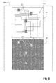
- the figure 3 represents in top view a mask blank BM1 with some defects F; the positions of these defects in the reference are precisely noted and introduced into a drawing calculation software which also contains the description elements of the drawing that is to be made in a photolithography operation on a sensitive surface to be exposed.
- the software establishes a unique mask pattern that will be used during the photolithography operation.
- the mask design is the complete design to be formed on the sensitive surface. It is specified here that there may be differences between the drawing to be made and the drawing of the mask used to form this drawing, for various technological reasons. Among these reasons is the need to introduce into the pattern of the mask optical proximity correction patterns (OPC patterns). It is recalled that OPC patterns are mask pattern modifications intended to compensate for exposure defects due to edge effects on boundaries, angles, etc. plots of the drawing. To simplify the explanations that follow, it is considered here that the drawing DE of the mask is generally the same as the drawing to be made.
- This mask drawing is contained in a computer file that is used to produce the mask from the mask blank; this file controls for example an electron beam writing machine.
- the figure 4 represents the mask blank BM1 with its defects, each surrounded by a respective exclusion zone ZE.
- the exclusion zones are represented with dimensions much greater than those which they have in reality.
- the defects are very small (a few hundred nanometers at most) and the exclusion zones can be squares or rectangles of a few micrometers apart.
- exclusion zones will be used to process the mask drawing file to produce two complementary files that take into account the exclusion zones.
- the figure 5 symbolically represents a DE mask pattern to be made on the sensitive surface of a silicon wafer. It is this drawing, or more precisely the descriptors of this drawing which are contained in the initial file.
- the drawing calculation software establishes two complementary mask patterns M1 and M2.
- the first mask pattern M1 is made on a mask blank BM1.
- the second is done on another white mask BM2.
- an inspection of the second mask is performed and it is verified that the second mask blank does not have defects in the same places as the first one.
- We could consider not checking the second mask blank because the probability that there will be defects in the same places as on the first is low, but it is still better to do this check and to choose as second mask white one another mask blank if there are defects placed in the same places in the two mask blanks.
- the two files describing the masks M1 and M2 are established taking into account drawing rules, and in particular rules making it possible to draw the boundaries of the exclusion zones around each defect.
- the first file has a main mask pattern M1 which is the desired drawing pattern DE from which elements placed in the exclusion zones ZE have been removed; the drawing becomes a DEp drawing which is the desired pattern but with missing parts replaced by black areas; black zone means areas that will not participate in the exposure of the surface to be treated; in a binary mask, these are the absorbent areas of the mask.
- the second file has a mask pattern M2 which is essentially a black area, except in zones ZEa which are identical in size, and in position in the drawing, to the exclusion zones ZE; these zones ZEa will be called: zones associated with the exclusion zones.
- the second file represents a mask drawing M2 constituted by the missing parts DEz of the drawing DE, and these missing parts are located in the associated zones ZEa; the rest of the file is black.
- the mask M1 made from the first file and the first mask blank BM1 is represented on the figure 6 ; it includes the main drawing DEp but no drawing in the exclusion zones ZE, black.
- the mask M2 made from the second file and the second mask blank BM2 is represented on the figure 7 ; it includes a complementary drawing DEz distributed only in the exclusion zones; everything else is black.
- this surface is successively exposed with the complementary masks M1 and M2 (the order is indifferent), taking care to use the same mark for align the surface to be treated with each mask.
- the exclusion zones belonging to the mask M1 and the zones associated with the exclusion zones belonging to the mask M2 are located at the same locations in the two masks; their projections are superimposed on the surface to be exposed.
- An exhibition machine which has a magazine capable of receiving a double mask M1 + M2.
- the alignment machine comprises a double plate for simultaneously receiving two silicon wafers to be treated, it is possible for example to proceed as follows: while the first wafer is exposed with the mask M1, the second wafer is pre-aligned. The second wafer is then exposed with the mask M1. Then we set up the M2 mask, we first expose the plate M1 then the plate M2. And we start the series of operations with a new set of two pads.
- exclusion zones can be arbitrary. Nevertheless, it may be preferable to use square, rectangular, or more generally polygonal exclusion zones (according to the main directions of the lines of the drawing) to simplify the program of calculation of the drawing files DEp and DEz from the drawing file DE.
- the black areas correspond to the absorbent areas of the mask.
- the pattern of the mask includes optical proximity correction patterns (OPC patterns)
- OPC patterns optical proximity correction patterns
- OPC patterns optical proximity correction patterns
- Providing a two-step exposure creates feature ends where there should not be, so an additional edge effect at the exclusion zone boundary; we can take it into account to modify the drawing at this point to compensate for this effect as we do for the rest of the drawing. This modification can be made in the vicinity of the boundaries of the exclusion zones and in the vicinity of the boundaries of the associated zones.
- the mask blank BM1 comprises two mask patterns M1 and M2 which are complementary and whose relative positions are perfectly defined so that the projections of these drawings can then be superposed during the two photolithography steps; the exclusion zones ZE of the first drawing M1 are located in the same relative places as the associated areas of the second drawing M2; during the photolithographic projection, they are then superimposed exactly on the associated zones ZEa of the second drawing, which contain the missing drawing patterns of the mask M1.
- the mask blank BM1 does not have defects in the associated areas ZEa, but statistically it is unlikely.
- the first mask pattern M1 is used separately to project the drawing DEp onto the surface to be exposed, and the second mask pattern M2, offset in the photolithography machine to put it in the position of projecting the complementary drawing DEz by superimposing exactly on the surface the exclusion zones ZE and the associated zones ZEa.
- the order of the steps is indifferent.
- the couples may be identical to each other (for multiple exposure of multiple chips) or different from each other if they correspond to different photolithography steps or to different patterns to be exposed simultaneously.
Applications Claiming Priority (1)
| Application Number | Priority Date | Filing Date | Title |
|---|---|---|---|
| FR1351759A FR3002655B1 (fr) | 2013-02-28 | 2013-02-28 | Procede de photolithographie a double masque minimisant l'impact des defauts de substrat |
Publications (2)
| Publication Number | Publication Date |
|---|---|
| EP2772802A1 true EP2772802A1 (de) | 2014-09-03 |
| EP2772802B1 EP2772802B1 (de) | 2016-08-17 |
Family
ID=48289375
Family Applications (1)
| Application Number | Title | Priority Date | Filing Date |
|---|---|---|---|
| EP14155467.5A Not-in-force EP2772802B1 (de) | 2013-02-28 | 2014-02-17 | Fotolithografieverfahren mit Doppelmaske, bei dem die Auswirkung von Substratfehlern minimiert ist |
Country Status (6)
| Country | Link |
|---|---|
| US (1) | US9116433B2 (de) |
| EP (1) | EP2772802B1 (de) |
| JP (1) | JP2014170935A (de) |
| KR (1) | KR20140108169A (de) |
| FR (1) | FR3002655B1 (de) |
| TW (1) | TW201502694A (de) |
Families Citing this family (2)
| Publication number | Priority date | Publication date | Assignee | Title |
|---|---|---|---|---|
| US9576099B2 (en) * | 2014-03-03 | 2017-02-21 | Taiwan Semiconductor Manufacturing Company, Ltd. | Minimizing harmful effects caused by reticle defects by re-arranging IC layout locally |
| US9612526B2 (en) | 2014-08-28 | 2017-04-04 | Taiwan Semiconductor Manufacturing Co., Ltd. | Photomask and method for fabricating integrated circuit |
Citations (3)
| Publication number | Priority date | Publication date | Assignee | Title |
|---|---|---|---|---|
| US5795685A (en) * | 1997-01-14 | 1998-08-18 | International Business Machines Corporation | Simple repair method for phase shifting masks |
| US20060093924A1 (en) * | 2004-11-03 | 2006-05-04 | International Business Machines Corporation | Method and apparatus for correction of defects in lithography masks |
| US20070158636A1 (en) * | 2005-12-22 | 2007-07-12 | Intel Corporation | Detecting and characterizing mask blank defects using angular distribution of scattered light |
Family Cites Families (20)
| Publication number | Priority date | Publication date | Assignee | Title |
|---|---|---|---|---|
| JP2001033941A (ja) * | 1999-07-16 | 2001-02-09 | Toshiba Corp | パターン形成方法及び露光装置 |
| FR2797060B1 (fr) * | 1999-07-29 | 2001-09-14 | Commissariat Energie Atomique | Structure pour masque de lithographie en reflexion et procede pour sa realisation |
| JP3768786B2 (ja) * | 2000-08-15 | 2006-04-19 | 株式会社ルネサステクノロジ | ホトマスクの製造方法、ホトマスクブランクスの製造方法およびホトマスクの再生方法 |
| DE10245204B4 (de) * | 2001-09-28 | 2008-02-07 | Hoya Corp. | Maskenrohling |
| TWI477890B (zh) * | 2004-06-22 | 2015-03-21 | Hoya Corp | Grayscale masking, grayscale mask, grayscale masking manufacturing method, manufacturing method of gray scale mask, and manufacturing method of liquid crystal display device |
| US7303842B2 (en) * | 2005-04-13 | 2007-12-04 | Kla-Tencor Technologies Corporation | Systems and methods for modifying a reticle's optical properties |
| FR2884965B1 (fr) * | 2005-04-26 | 2007-06-08 | Commissariat Energie Atomique | Structure de blanc de masque ajustable pour masque euv a decalage de phase |
| FR2894691B1 (fr) * | 2005-12-13 | 2008-01-18 | Commissariat Energie Atomique | Procede de fabrication de masque lithographique en reflexion et masque issu du procede |
| US7927766B2 (en) * | 2008-03-03 | 2011-04-19 | International Business Machines Corporation | Pre-alignment marking and inspection to improve mask substrate defect tolerance |
| JP5155017B2 (ja) * | 2008-05-29 | 2013-02-27 | ルネサスエレクトロニクス株式会社 | 半導体集積回路装置の製造方法 |
| EP2443651B1 (de) * | 2009-06-19 | 2015-08-12 | KLA-Tencor Corporation | Inspektionssysteme und verfahren zur defekterkennung auf euv maskenrohlingen |
| TWI553399B (zh) * | 2009-07-16 | 2016-10-11 | Hoya Corp | Mask base and transfer mask |
| WO2011108470A1 (ja) * | 2010-03-02 | 2011-09-09 | 旭硝子株式会社 | Euvリソグラフィ用反射型マスクブランクおよびその製造方法 |
| WO2012125581A2 (en) * | 2011-03-15 | 2012-09-20 | Kla-Tencor Corporation | Method and apparatus for inspecting a reflective lithographic mask blank and improving mask quality |
| JP5684028B2 (ja) * | 2011-03-31 | 2015-03-11 | Hoya株式会社 | 転写用マスクの製造方法および半導体デバイスの製造方法 |
| US8802334B2 (en) * | 2011-04-06 | 2014-08-12 | Hoya Corporation | Surface treatment method for a mask blank, method of manufacturing a mask blank, and method of manufacturing a mask |
| JP5758727B2 (ja) * | 2011-07-15 | 2015-08-05 | ルネサスエレクトロニクス株式会社 | マスク検査方法、およびマスク検査装置 |
| US9075934B2 (en) * | 2011-09-24 | 2015-07-07 | Globalfoundries Inc. | Reticle defect correction by second exposure |
| US8726202B2 (en) * | 2012-04-13 | 2014-05-13 | International Business Machines Corporation | Mitigation of mask defects by pattern shifting |
| US8932785B2 (en) * | 2012-10-16 | 2015-01-13 | Advanced Mask Technology Center Gmbh & Co. Kg | EUV mask set and methods of manufacturing EUV masks and integrated circuits |
-
2013
- 2013-02-28 FR FR1351759A patent/FR3002655B1/fr not_active Expired - Fee Related
-
2014
- 2014-02-17 EP EP14155467.5A patent/EP2772802B1/de not_active Not-in-force
- 2014-02-25 TW TW103106278A patent/TW201502694A/zh unknown
- 2014-02-25 US US14/189,835 patent/US9116433B2/en not_active Expired - Fee Related
- 2014-02-27 JP JP2014036949A patent/JP2014170935A/ja active Pending
- 2014-02-27 KR KR1020140023720A patent/KR20140108169A/ko not_active Application Discontinuation
Patent Citations (3)
| Publication number | Priority date | Publication date | Assignee | Title |
|---|---|---|---|---|
| US5795685A (en) * | 1997-01-14 | 1998-08-18 | International Business Machines Corporation | Simple repair method for phase shifting masks |
| US20060093924A1 (en) * | 2004-11-03 | 2006-05-04 | International Business Machines Corporation | Method and apparatus for correction of defects in lithography masks |
| US20070158636A1 (en) * | 2005-12-22 | 2007-07-12 | Intel Corporation | Detecting and characterizing mask blank defects using angular distribution of scattered light |
Non-Patent Citations (1)
| Title |
|---|
| ABDE ALI KAGALWALLA ET AL: "Design-Aware Defect-Avoidance Floorplanning of EUV Masks", IEEE TRANSACTIONS ON SEMICONDUCTOR MANUFACTURING, IEEE SERVICE CENTER, PISCATAWAY, NJ, US, vol. 26, no. 1, 30 January 2013 (2013-01-30), pages 111 - 124, XP011491658, ISSN: 0894-6507, DOI: 10.1109/TSM.2012.2234151 * |
Also Published As
| Publication number | Publication date |
|---|---|
| JP2014170935A (ja) | 2014-09-18 |
| FR3002655B1 (fr) | 2016-05-13 |
| EP2772802B1 (de) | 2016-08-17 |
| US20140242522A1 (en) | 2014-08-28 |
| TW201502694A (zh) | 2015-01-16 |
| FR3002655A1 (fr) | 2014-08-29 |
| US9116433B2 (en) | 2015-08-25 |
| KR20140108169A (ko) | 2014-09-05 |
Similar Documents
| Publication | Publication Date | Title |
|---|---|---|
| EP2701005B1 (de) | Herstellungsverfahren von EUV-Masken, die den Einfluss von Substratdefekten minimieren | |
| US9075934B2 (en) | Reticle defect correction by second exposure | |
| KR100647182B1 (ko) | 포토마스크, 포토마스크의 제조 방법, 및 그 포토마스크를이용한 반도체 장치의 제조 방법 | |
| TW201005799A (en) | Manufacturing method of semiconductor integrated circuit device | |
| FR2598233A1 (fr) | Procede de fabrication d'un substrat a circuits integres comprenant differents des independants | |
| KR100532641B1 (ko) | 마스크 기판 및 그 제조 방법 | |
| JP2006013494A (ja) | 反射マスク、反射マスクの使用および反射マスクを製造する方法 | |
| EP2772802B1 (de) | Fotolithografieverfahren mit Doppelmaske, bei dem die Auswirkung von Substratfehlern minimiert ist | |
| JP2008116517A (ja) | 中間調フォトマスク及びその製造方法 | |
| JP2011186506A (ja) | 中間調フォトマスク | |
| JP3312703B2 (ja) | 位相シフトフォトマスクの修正方法 | |
| JP5816499B2 (ja) | Euvマスクの製造方法 | |
| JP5943306B2 (ja) | 反射型マスクの製造方法およびマスクブランクの製造方法 | |
| JP2013055197A (ja) | 露光方法及び露光用マスク | |
| JP3630929B2 (ja) | ハーフトーン型位相シフトマスクの製造方法 | |
| US9535317B2 (en) | Treating a capping layer of a mask | |
| US9897910B2 (en) | Treating a capping layer of a mask | |
| JP2015141972A (ja) | Euvマスクおよびeuvマスクの製造方法 | |
| KR101179000B1 (ko) | 다계조 광마스크 및 그 수정방법 | |
| US20220163881A1 (en) | Phase-shift reticle for use in photolithography | |
| EP1695145B1 (de) | Verfharen zur korrektur von fehlerhaften motiven in dünnen schichten | |
| CN115981094A (zh) | 光罩、光罩的制作方法及使用该光罩的图案形成方法 | |
| TW552470B (en) | Method for repairing mask by using multiple phase steps | |
| JP5283441B2 (ja) | 多階調フォトマスク及びその修正方法 | |
| US20050026049A1 (en) | Method for forming an opening on an alternating phase shift mask |
Legal Events
| Date | Code | Title | Description |
|---|---|---|---|
| PUAI | Public reference made under article 153(3) epc to a published international application that has entered the european phase |
Free format text: ORIGINAL CODE: 0009012 |
|
| 17P | Request for examination filed |
Effective date: 20140217 |
|
| AK | Designated contracting states |
Kind code of ref document: A1 Designated state(s): AL AT BE BG CH CY CZ DE DK EE ES FI FR GB GR HR HU IE IS IT LI LT LU LV MC MK MT NL NO PL PT RO RS SE SI SK SM TR |
|
| AX | Request for extension of the european patent |
Extension state: BA ME |
|
| R17P | Request for examination filed (corrected) |
Effective date: 20150224 |
|
| RBV | Designated contracting states (corrected) |
Designated state(s): AL AT BE BG CH CY CZ DE DK EE ES FI FR GB GR HR HU IE IS IT LI LT LU LV MC MK MT NL NO PL PT RO RS SE SI SK SM TR |
|
| GRAP | Despatch of communication of intention to grant a patent |
Free format text: ORIGINAL CODE: EPIDOSNIGR1 |
|
| INTG | Intention to grant announced |
Effective date: 20160405 |
|
| RAP1 | Party data changed (applicant data changed or rights of an application transferred) |
Owner name: COMMISSARIAT A L'ENERGIE ATOMIQUE ET AUX ENERGIES |
|
| GRAS | Grant fee paid |
Free format text: ORIGINAL CODE: EPIDOSNIGR3 |
|
| GRAA | (expected) grant |
Free format text: ORIGINAL CODE: 0009210 |
|
| AK | Designated contracting states |
Kind code of ref document: B1 Designated state(s): AL AT BE BG CH CY CZ DE DK EE ES FI FR GB GR HR HU IE IS IT LI LT LU LV MC MK MT NL NO PL PT RO RS SE SI SK SM TR |
|
| REG | Reference to a national code |
Ref country code: GB Ref legal event code: FG4D Free format text: NOT ENGLISH |
|
| REG | Reference to a national code |
Ref country code: CH Ref legal event code: EP |
|
| REG | Reference to a national code |
Ref country code: IE Ref legal event code: FG4D Free format text: LANGUAGE OF EP DOCUMENT: FRENCH |
|
| REG | Reference to a national code |
Ref country code: AT Ref legal event code: REF Ref document number: 821632 Country of ref document: AT Kind code of ref document: T Effective date: 20160915 |
|
| REG | Reference to a national code |
Ref country code: DE Ref legal event code: R096 Ref document number: 602014003015 Country of ref document: DE |
|
| REG | Reference to a national code |
Ref country code: NL Ref legal event code: MP Effective date: 20160817 |
|
| REG | Reference to a national code |
Ref country code: LT Ref legal event code: MG4D |
|
| REG | Reference to a national code |
Ref country code: AT Ref legal event code: MK05 Ref document number: 821632 Country of ref document: AT Kind code of ref document: T Effective date: 20160817 |
|
| PG25 | Lapsed in a contracting state [announced via postgrant information from national office to epo] |
Ref country code: NO Free format text: LAPSE BECAUSE OF FAILURE TO SUBMIT A TRANSLATION OF THE DESCRIPTION OR TO PAY THE FEE WITHIN THE PRESCRIBED TIME-LIMIT Effective date: 20161117 Ref country code: FI Free format text: LAPSE BECAUSE OF FAILURE TO SUBMIT A TRANSLATION OF THE DESCRIPTION OR TO PAY THE FEE WITHIN THE PRESCRIBED TIME-LIMIT Effective date: 20160817 Ref country code: IT Free format text: LAPSE BECAUSE OF FAILURE TO SUBMIT A TRANSLATION OF THE DESCRIPTION OR TO PAY THE FEE WITHIN THE PRESCRIBED TIME-LIMIT Effective date: 20160817 Ref country code: RS Free format text: LAPSE BECAUSE OF FAILURE TO SUBMIT A TRANSLATION OF THE DESCRIPTION OR TO PAY THE FEE WITHIN THE PRESCRIBED TIME-LIMIT Effective date: 20160817 Ref country code: LT Free format text: LAPSE BECAUSE OF FAILURE TO SUBMIT A TRANSLATION OF THE DESCRIPTION OR TO PAY THE FEE WITHIN THE PRESCRIBED TIME-LIMIT Effective date: 20160817 Ref country code: HR Free format text: LAPSE BECAUSE OF FAILURE TO SUBMIT A TRANSLATION OF THE DESCRIPTION OR TO PAY THE FEE WITHIN THE PRESCRIBED TIME-LIMIT Effective date: 20160817 Ref country code: NL Free format text: LAPSE BECAUSE OF FAILURE TO SUBMIT A TRANSLATION OF THE DESCRIPTION OR TO PAY THE FEE WITHIN THE PRESCRIBED TIME-LIMIT Effective date: 20160817 |
|
| PG25 | Lapsed in a contracting state [announced via postgrant information from national office to epo] |
Ref country code: PL Free format text: LAPSE BECAUSE OF FAILURE TO SUBMIT A TRANSLATION OF THE DESCRIPTION OR TO PAY THE FEE WITHIN THE PRESCRIBED TIME-LIMIT Effective date: 20160817 Ref country code: LV Free format text: LAPSE BECAUSE OF FAILURE TO SUBMIT A TRANSLATION OF THE DESCRIPTION OR TO PAY THE FEE WITHIN THE PRESCRIBED TIME-LIMIT Effective date: 20160817 Ref country code: SE Free format text: LAPSE BECAUSE OF FAILURE TO SUBMIT A TRANSLATION OF THE DESCRIPTION OR TO PAY THE FEE WITHIN THE PRESCRIBED TIME-LIMIT Effective date: 20160817 Ref country code: PT Free format text: LAPSE BECAUSE OF FAILURE TO SUBMIT A TRANSLATION OF THE DESCRIPTION OR TO PAY THE FEE WITHIN THE PRESCRIBED TIME-LIMIT Effective date: 20161219 Ref country code: ES Free format text: LAPSE BECAUSE OF FAILURE TO SUBMIT A TRANSLATION OF THE DESCRIPTION OR TO PAY THE FEE WITHIN THE PRESCRIBED TIME-LIMIT Effective date: 20160817 Ref country code: AT Free format text: LAPSE BECAUSE OF FAILURE TO SUBMIT A TRANSLATION OF THE DESCRIPTION OR TO PAY THE FEE WITHIN THE PRESCRIBED TIME-LIMIT Effective date: 20160817 Ref country code: GR Free format text: LAPSE BECAUSE OF FAILURE TO SUBMIT A TRANSLATION OF THE DESCRIPTION OR TO PAY THE FEE WITHIN THE PRESCRIBED TIME-LIMIT Effective date: 20161118 |
|
| PG25 | Lapsed in a contracting state [announced via postgrant information from national office to epo] |
Ref country code: EE Free format text: LAPSE BECAUSE OF FAILURE TO SUBMIT A TRANSLATION OF THE DESCRIPTION OR TO PAY THE FEE WITHIN THE PRESCRIBED TIME-LIMIT Effective date: 20160817 Ref country code: RO Free format text: LAPSE BECAUSE OF FAILURE TO SUBMIT A TRANSLATION OF THE DESCRIPTION OR TO PAY THE FEE WITHIN THE PRESCRIBED TIME-LIMIT Effective date: 20160817 |
|
| REG | Reference to a national code |
Ref country code: DE Ref legal event code: R097 Ref document number: 602014003015 Country of ref document: DE |
|
| PG25 | Lapsed in a contracting state [announced via postgrant information from national office to epo] |
Ref country code: CZ Free format text: LAPSE BECAUSE OF FAILURE TO SUBMIT A TRANSLATION OF THE DESCRIPTION OR TO PAY THE FEE WITHIN THE PRESCRIBED TIME-LIMIT Effective date: 20160817 Ref country code: BG Free format text: LAPSE BECAUSE OF FAILURE TO SUBMIT A TRANSLATION OF THE DESCRIPTION OR TO PAY THE FEE WITHIN THE PRESCRIBED TIME-LIMIT Effective date: 20161117 Ref country code: SM Free format text: LAPSE BECAUSE OF FAILURE TO SUBMIT A TRANSLATION OF THE DESCRIPTION OR TO PAY THE FEE WITHIN THE PRESCRIBED TIME-LIMIT Effective date: 20160817 Ref country code: SK Free format text: LAPSE BECAUSE OF FAILURE TO SUBMIT A TRANSLATION OF THE DESCRIPTION OR TO PAY THE FEE WITHIN THE PRESCRIBED TIME-LIMIT Effective date: 20160817 Ref country code: DK Free format text: LAPSE BECAUSE OF FAILURE TO SUBMIT A TRANSLATION OF THE DESCRIPTION OR TO PAY THE FEE WITHIN THE PRESCRIBED TIME-LIMIT Effective date: 20160817 Ref country code: BE Free format text: LAPSE BECAUSE OF NON-PAYMENT OF DUE FEES Effective date: 20170228 |
|
| PLBE | No opposition filed within time limit |
Free format text: ORIGINAL CODE: 0009261 |
|
| STAA | Information on the status of an ep patent application or granted ep patent |
Free format text: STATUS: NO OPPOSITION FILED WITHIN TIME LIMIT |
|
| 26N | No opposition filed |
Effective date: 20170518 |
|
| PG25 | Lapsed in a contracting state [announced via postgrant information from national office to epo] |
Ref country code: SI Free format text: LAPSE BECAUSE OF FAILURE TO SUBMIT A TRANSLATION OF THE DESCRIPTION OR TO PAY THE FEE WITHIN THE PRESCRIBED TIME-LIMIT Effective date: 20160817 |
|
| REG | Reference to a national code |
Ref country code: DE Ref legal event code: R119 Ref document number: 602014003015 Country of ref document: DE |
|
| PG25 | Lapsed in a contracting state [announced via postgrant information from national office to epo] |
Ref country code: MC Free format text: LAPSE BECAUSE OF FAILURE TO SUBMIT A TRANSLATION OF THE DESCRIPTION OR TO PAY THE FEE WITHIN THE PRESCRIBED TIME-LIMIT Effective date: 20160817 |
|
| REG | Reference to a national code |
Ref country code: CH Ref legal event code: PL |
|
| PG25 | Lapsed in a contracting state [announced via postgrant information from national office to epo] |
Ref country code: LI Free format text: LAPSE BECAUSE OF NON-PAYMENT OF DUE FEES Effective date: 20170228 Ref country code: CH Free format text: LAPSE BECAUSE OF NON-PAYMENT OF DUE FEES Effective date: 20170228 |
|
| REG | Reference to a national code |
Ref country code: IE Ref legal event code: MM4A |
|
| REG | Reference to a national code |
Ref country code: FR Ref legal event code: ST Effective date: 20171031 |
|
| PG25 | Lapsed in a contracting state [announced via postgrant information from national office to epo] |
Ref country code: LU Free format text: LAPSE BECAUSE OF NON-PAYMENT OF DUE FEES Effective date: 20170217 |
|
| PG25 | Lapsed in a contracting state [announced via postgrant information from national office to epo] |
Ref country code: FR Free format text: LAPSE BECAUSE OF NON-PAYMENT OF DUE FEES Effective date: 20170228 Ref country code: DE Free format text: LAPSE BECAUSE OF NON-PAYMENT OF DUE FEES Effective date: 20170901 |
|
| REG | Reference to a national code |
Ref country code: BE Ref legal event code: MM Effective date: 20170228 |
|
| PG25 | Lapsed in a contracting state [announced via postgrant information from national office to epo] |
Ref country code: IE Free format text: LAPSE BECAUSE OF NON-PAYMENT OF DUE FEES Effective date: 20170217 |
|
| PG25 | Lapsed in a contracting state [announced via postgrant information from national office to epo] |
Ref country code: MT Free format text: LAPSE BECAUSE OF FAILURE TO SUBMIT A TRANSLATION OF THE DESCRIPTION OR TO PAY THE FEE WITHIN THE PRESCRIBED TIME-LIMIT Effective date: 20160817 |
|
| GBPC | Gb: european patent ceased through non-payment of renewal fee |
Effective date: 20180217 |
|
| PG25 | Lapsed in a contracting state [announced via postgrant information from national office to epo] |
Ref country code: AL Free format text: LAPSE BECAUSE OF FAILURE TO SUBMIT A TRANSLATION OF THE DESCRIPTION OR TO PAY THE FEE WITHIN THE PRESCRIBED TIME-LIMIT Effective date: 20160817 |
|
| PG25 | Lapsed in a contracting state [announced via postgrant information from national office to epo] |
Ref country code: GB Free format text: LAPSE BECAUSE OF NON-PAYMENT OF DUE FEES Effective date: 20180217 |
|
| PG25 | Lapsed in a contracting state [announced via postgrant information from national office to epo] |
Ref country code: HU Free format text: LAPSE BECAUSE OF FAILURE TO SUBMIT A TRANSLATION OF THE DESCRIPTION OR TO PAY THE FEE WITHIN THE PRESCRIBED TIME-LIMIT; INVALID AB INITIO Effective date: 20140217 |
|
| PG25 | Lapsed in a contracting state [announced via postgrant information from national office to epo] |
Ref country code: CY Free format text: LAPSE BECAUSE OF NON-PAYMENT OF DUE FEES Effective date: 20160817 |
|
| PG25 | Lapsed in a contracting state [announced via postgrant information from national office to epo] |
Ref country code: MK Free format text: LAPSE BECAUSE OF FAILURE TO SUBMIT A TRANSLATION OF THE DESCRIPTION OR TO PAY THE FEE WITHIN THE PRESCRIBED TIME-LIMIT Effective date: 20160817 |
|
| PG25 | Lapsed in a contracting state [announced via postgrant information from national office to epo] |
Ref country code: TR Free format text: LAPSE BECAUSE OF FAILURE TO SUBMIT A TRANSLATION OF THE DESCRIPTION OR TO PAY THE FEE WITHIN THE PRESCRIBED TIME-LIMIT Effective date: 20160817 |
|
| PG25 | Lapsed in a contracting state [announced via postgrant information from national office to epo] |
Ref country code: IS Free format text: LAPSE BECAUSE OF FAILURE TO SUBMIT A TRANSLATION OF THE DESCRIPTION OR TO PAY THE FEE WITHIN THE PRESCRIBED TIME-LIMIT Effective date: 20161217 |