EP2770632B1 - Measurement of DC offsets in IQ modulators - Google Patents
Measurement of DC offsets in IQ modulators Download PDFInfo
- Publication number
- EP2770632B1 EP2770632B1 EP14156198.5A EP14156198A EP2770632B1 EP 2770632 B1 EP2770632 B1 EP 2770632B1 EP 14156198 A EP14156198 A EP 14156198A EP 2770632 B1 EP2770632 B1 EP 2770632B1
- Authority
- EP
- European Patent Office
- Prior art keywords
- modulator
- offset
- input
- determining
- functions
- Prior art date
- Legal status (The legal status is an assumption and is not a legal conclusion. Google has not performed a legal analysis and makes no representation as to the accuracy of the status listed.)
- Not-in-force
Links
Images


Classifications
-
- H—ELECTRICITY
- H04—ELECTRIC COMMUNICATION TECHNIQUE
- H04B—TRANSMISSION
- H04B17/00—Monitoring; Testing
- H04B17/10—Monitoring; Testing of transmitters
- H04B17/101—Monitoring; Testing of transmitters for measurement of specific parameters of the transmitter or components thereof
- H04B17/104—Monitoring; Testing of transmitters for measurement of specific parameters of the transmitter or components thereof of other parameters, e.g. DC offset, delay or propagation times
-
- H—ELECTRICITY
- H03—ELECTRONIC CIRCUITRY
- H03C—MODULATION
- H03C3/00—Angle modulation
- H03C3/38—Angle modulation by converting amplitude modulation to angle modulation
- H03C3/40—Angle modulation by converting amplitude modulation to angle modulation using two signal paths the outputs of which have a predetermined phase difference and at least one output being amplitude-modulated
-
- H—ELECTRICITY
- H04—ELECTRIC COMMUNICATION TECHNIQUE
- H04L—TRANSMISSION OF DIGITAL INFORMATION, e.g. TELEGRAPHIC COMMUNICATION
- H04L27/00—Modulated-carrier systems
- H04L27/32—Carrier systems characterised by combinations of two or more of the types covered by groups H04L27/02, H04L27/10, H04L27/18 or H04L27/26
- H04L27/34—Amplitude- and phase-modulated carrier systems, e.g. quadrature-amplitude modulated carrier systems
- H04L27/36—Modulator circuits; Transmitter circuits
- H04L27/362—Modulation using more than one carrier, e.g. with quadrature carriers, separately amplitude modulated
- H04L27/364—Arrangements for overcoming imperfections in the modulator, e.g. quadrature error or unbalanced I and Q levels
-
- H—ELECTRICITY
- H04—ELECTRIC COMMUNICATION TECHNIQUE
- H04L—TRANSMISSION OF DIGITAL INFORMATION, e.g. TELEGRAPHIC COMMUNICATION
- H04L27/00—Modulated-carrier systems
- H04L27/32—Carrier systems characterised by combinations of two or more of the types covered by groups H04L27/02, H04L27/10, H04L27/18 or H04L27/26
- H04L27/34—Amplitude- and phase-modulated carrier systems, e.g. quadrature-amplitude modulated carrier systems
- H04L27/38—Demodulator circuits; Receiver circuits
- H04L27/3845—Demodulator circuits; Receiver circuits using non - coherent demodulation, i.e. not using a phase synchronous carrier
- H04L27/3854—Demodulator circuits; Receiver circuits using non - coherent demodulation, i.e. not using a phase synchronous carrier using a non - coherent carrier, including systems with baseband correction for phase or frequency offset
Definitions
- This disclosure is directed to systems and methods for measuring parameters in IQ modulators, and, more particularly, to systems and methods of measuring offset voltages commonly called DC offsets in IQ modulators.
- IQ modulators are well known in the field of RF and microwave communications, finding use in both analog and digital modulation formats.
- IQ modulation is a method of modulating a carrier wave, which is typically but not always sinusoidal, with two baseband input signals. The two signals are oftentimes referred to as I (in-channel) and Q (quadrature-phase) components.
- Fig. 1 is a block diagram of an example conventional I-Q modulator 5. It contains a local oscillator (or "LO") 10 producing sinusoidal signals at a carrier frequency, designated as ⁇ c .
- the LO 10 has two outputs, which are of equal magnitude and differ in phase by exactly 90 degrees.
- the signal from the LO 10 are multiplied in mixers 12, 14 by two independent baseband inputs, the I and Q inputs. These products of the I and Q inputs and the carrier frequency ⁇ c are summed to yield the frequency-converted result.
- Baseband inputs may contain any arbitrary waveforms, although the bandwidth of these is usually less than the carrier frequency.
- the baseband inputs are designated as x (in-phase) and y (quadrature), while the two LO signals are designated I and Q.
- the I-Q modulator 5 up-converts the real-valued baseband inputs ⁇ x, y ⁇ as if taken together, they were together a complex-valued input (x + jy).
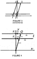
- Fig. 2 is a phasor diagram showing an ideal I vector 20 and an ideal Q vector 22.
- ideal modulators will generate I and Q channels that have exactly the same amplitude gain across the desired frequencies, and will be out of phase from one another by exactly 90 degrees, real-world implementations of the I and Q signals do not have identical magnitudes and do not differ in phase by exactly 90 degrees.
- Additional non-ideal aspects of the I-Q modulator such as differing gains and phases between the two mixers, can also be modeled as amplitude and phase imbalances between the I and Q LO signals. These imbalances may affect the quality of the generated signal from the modulator.
- This error itself may be represented in the phasor diagram.
- this errant Q vector is depicted by the vector 24.
- Such errors are also referred to as "IQ imbalance,” and often vary with changes in operating parameters, such as carrier frequency and drive power of the local oscillator 10.
- Imperfections in the design and construction of IQ modulators result in apparent DC offsets being present at the ⁇ x, y ⁇ inputs. This causes problems with the modulated signal at exactly the carrier frequency. Often it is desirable to remove the signal component at the carrier frequency. To achieve this result in a modulated signal, the analog waveforms presented at the ⁇ x, y ⁇ inputs would normally be designed to have a zero average DC level. Unfortunately, DC offsets in the modulator result in an undesired signal component at the carrier frequency under these conditions.
- Fig.3 One conventional method for measuring DC offset is illustrated in Fig.3 .
- the DC average of the x input is adjusted to minimize the carrier signal amplitude. Generally this will not reduce the carrier amplitude to zero because of the unknown DC offset present at the y input of the modulator.
- the standard way to measure offset becomes an iterative process, where first DC average of the x input is first adjusted, then the y input is adjusted. Adjusting the y input, however, affects the x offset, so then the x input is adjusted again, followed by the y input being adjusted again.
- Embodiments of the invention address these and other limitations of the prior art.
- a method of determining a DC offset in an IQ modulator which comprises a first and second input which are respectively a quadrature and an in-phase input.
- a device for determining a DC offset in an IQ modulator as set out in claim 7.
- aspects of the invention include a method of determining a DC offset in an IQ modulator, including selecting a first and a second voltage for a first input to an IQ modulator, such as the Q input. Then, for each of the first and second voltages applied to the Q input, applying a set of input signals to a second input of the IQ modulator, such as the I input, and generating a respective set of measured parameters from an output of the IQ modulator.
- generating the measured parameters may include determining carrier power.
- the method may include generating a first, second-order polynomial function from the set of measured parameters related to the first voltage of the first input of the IQ modulator as well as generating a second, second-order polynomial function from the set of measured parameters related to the second voltage of the first input of the IQ modulator.
- the second-order polynomial function may be a parabola. Then factors of the first and second functions may be compared to determine a relationship of the first and second functions to one another, and the DC offset determined from the determined relationship of the functions.
- Such a device may include a first input, such as a Q input, to an IQ modulator at which a first and a second voltage may be accepted and a second input to the IQ modulator at which, for each of the first and second voltage, a set of input signals may be applied.
- the second input may be the I input and may include, for example, three or more signals.
- a detector is structured to generate a respective set of measured parameters from an output of the IQ modulator for each of the set of input signals, and a function generator is structured to generate polynomial functions from the measured parameters, such as a parabola. Once the functions are generated, a comparator can be used to compare factors of the generated polynomial functions, such as a power level, to one another to generate a relationship between the measured parameters. Then an offset calculator can determine the DC offset from the determined relationship.
- Embodiments of the invention are directed to systems and methods for determining DC offset that are non-iterative and can work with as few as six measurements.
- a mathematical framework will aid in understanding the algorithm.
- v I is the purposely applied voltage
- ⁇ I is the DC offset
- Fig. 4 graphically illustrates a vector summation.
- Two different lengths of the Q vector are illustrated as reference 210.
- a one-dimensional sub-space accessible by altering the I vector magnitude is shown as the lines 220, 230.
- the I vector 222, 232, respectively when added to the corresponding Q vector, minimizes the length of the resultant vector. This corresponds to the minimum possible carrier amplitude for each of the two Q vectors.
- the power function P(*) is quadratic in the other variable, and also therefore in the input voltage, vI or vQ. This observation allows a new method for determining the points P1, P2 in Fig. 4 .
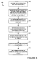
- FIG. 5 is a flow diagram illustrating an example method according to embodiments of the invention.
- a flow 500 begins at an operation 510 where two different DC test voltages for v Q are chosen.
- the selected voltages differ by approximately the expected DC offset value, and are also large enough to produce a measurable carrier amplitude.
- the first selected test voltage is applied to the Q input and the carrier power measured with at least three different DC voltages applied to the I input.
- more than three measurements may be made, especially when system noise or measurement resolution is a consideration. Again, for numerical accuracy, it is also better that these voltages differ by amounts as described with reference to operation 510 above.
- an operation 540 determines the minimum point of the polynomial function. This is ⁇ v I1 , v Q1 , P 1 ⁇ .
- the operations 520, 530, and 540 are repeated for the second Q test voltage to get ⁇ v I2 , v Q2 , P 2 ⁇ .
- the three I test voltages may be shifted to straddle the point v I1 .
- the r value computed in the operation 560 is used to compute the DC offsets ⁇ Q and ⁇ I using equations 2 and 3, respectively.
- DC offsets are computed, special cases may be evaluated. For example, if r computed in the operation 560 is close to one, then the second test voltages for I may be changed and the process run again. also, if v I1 and v I2 are nearly identical, then ⁇ I is approximately equal to their average. Further, if one of the carrier powers is zero, then the exact DC offsets were initially selected and no further calculations are necessary.
- an exemplary embodiment of the invention may include a method of determining a DC offset in an IQ modulator, including selecting a first and a second voltage for a first input to an IQ modulator, such as the Q input. Then, for each of the first and second voltages applied to the Q input, applying a set of input signals to a second input of the IQ modulator, such as the I input, and generating a respective set of measured parameters from an output of the IQ modulator.
- generating the measured parameters may include determining carrier power.
- the method may include generating a first, second-order polynomial function from the set of measured parameters related to the first voltage of the first input of the IQ modulator as well as generating a second, second-order polynomial function from the set of measured parameters related to the second voltage of the first input of the IQ modulator.
- the second-order polynomial function may be a parabola. Then factors of the first and second functions may be compared to determine a relationship of the first and second functions to one another, and the DC offset determined from the determined relationship of the functions.
- the method may further include, for instance, determining a minimum of the first and second-order polynomial function and determining a power level from the minimum of the first and second-order polynomial functions.
- Fig. 6 is a functional block diagram of a component 600 that includes a voltage offset measurer 652.
- the offset measurer 652 may also be combined with compensation circuitry so that an IQ modulator 610 the component 600 may be self-calibrated.
- the offset measurer may measure the DC offset of the IQ modulator 610 using the techniques described above and then compensate the modulator 610 by the measured amount to make the IQ modulator most efficient.
- the offset measurer 652 may be in another instrument (not shown) coupled to the component 600 and used to measure or compensate for DC offset in the IQ modulator 610.
- the offset measurer may be embodied in software stored in a memory 659 or other computer readable medium that may be executed by a processor 658 to produce the DC measurements or compensation.
- a device for determining a DC offset in an IQ modulator includes a first input, such as a Q input, to an IQ modulator at which a first and a second voltage may be accepted and a second input to the IQ modulator at which, for each of the first and second voltage, a set of input signals may be applied.
- the second input may be the I input and may include, for example, three or mor signals.
- a detector is structured to generate a respective set of measured parameters from an output of the IQ modulator for each of the set of input signals, and a function generator is structured to generate polynomial functions from the measured parameters, such as a parabola. Once the functions are generated, a comparator can be used to compare factors of the generated polynomial functions, such as a power level, to one another to generate a relationship between the measured parameters. Then an offset calculator can determine the DC offset from the determined relationship.
- Embodiments may also include a minimum detector structured to detect a minimum of the generated polynomial functions, as well as a power detector structured to determine a power level from the minimum of the polynomial functions.
- the device may be embodied in an instrument, and further, may be included in a self-calibration circuit to the instrument itself.
Landscapes
- Engineering & Computer Science (AREA)
- Computer Networks & Wireless Communication (AREA)
- Signal Processing (AREA)
- Physics & Mathematics (AREA)
- Electromagnetism (AREA)
- Digital Transmission Methods That Use Modulated Carrier Waves (AREA)
Applications Claiming Priority (1)
| Application Number | Priority Date | Filing Date | Title |
|---|---|---|---|
| US13/774,565 US9025648B2 (en) | 2013-02-22 | 2013-02-22 | Measurement of DC offsets in IQ modulators |
Publications (2)
| Publication Number | Publication Date |
|---|---|
| EP2770632A1 EP2770632A1 (en) | 2014-08-27 |
| EP2770632B1 true EP2770632B1 (en) | 2015-09-09 |
Family
ID=50156607
Family Applications (1)
| Application Number | Title | Priority Date | Filing Date |
|---|---|---|---|
| EP14156198.5A Not-in-force EP2770632B1 (en) | 2013-02-22 | 2014-02-21 | Measurement of DC offsets in IQ modulators |
Country Status (5)
| Country | Link |
|---|---|
| US (1) | US9025648B2 (ko) |
| EP (1) | EP2770632B1 (ko) |
| JP (1) | JP6415825B2 (ko) |
| KR (1) | KR20140105409A (ko) |
| CN (1) | CN104022834B (ko) |
Families Citing this family (4)
| Publication number | Priority date | Publication date | Assignee | Title |
|---|---|---|---|---|
| US9742600B2 (en) | 2015-02-05 | 2017-08-22 | Samsung Electronics Co., Ltd. | Method and system for estimating and compensating for direct current (DC) offset in ultra-low power (ULP) receiver |
| US10470070B1 (en) * | 2018-06-20 | 2019-11-05 | Viavi Solutions Inc. | Radio frequency (RF) power measurements in common public radio interface (CPRI) spectrum analysis |
| CN112737610B (zh) * | 2020-12-29 | 2023-07-07 | 芯翼信息科技(上海)有限公司 | 直流偏移的估计和校准方法及装置 |
| US11683026B1 (en) | 2022-08-30 | 2023-06-20 | International Business Machines Corporation | Calibrating signal currents in a radio frequency signal generator |
Family Cites Families (16)
| Publication number | Priority date | Publication date | Assignee | Title |
|---|---|---|---|---|
| FR2785111B1 (fr) * | 1998-10-23 | 2004-08-20 | St Microelectronics Sa | Procede et systeme de reglage du niveau des raies parasites du spectre frequentiel de sortie d'un dispositif de transposition de frequence a bande laterale unique, en particulier incorpore dans un telephone mobile |
| US6298096B1 (en) * | 1998-11-19 | 2001-10-02 | Titan Corporation | Method and apparatus for determination of predistortion parameters for a quadrature modulator |
| US6421398B1 (en) * | 2000-01-28 | 2002-07-16 | Alcatel Canada Inc. | Modulation system having on-line IQ calibration |
| US6801581B1 (en) | 2000-09-13 | 2004-10-05 | Intel Corporation | DC offset cancellation |
| US7003263B2 (en) | 2003-05-12 | 2006-02-21 | Lucent Technologies Inc. | Telecommunications receiver and a transmitter |
| US7369813B2 (en) * | 2003-05-14 | 2008-05-06 | Telefonaktiebolaget L M Ericsson (Publ) | Fast calibration of electronic components |
| US7376200B2 (en) * | 2003-06-06 | 2008-05-20 | Interdigital Technology Corporation | Method and apparatus for suppressing carrier leakage |
| US7280619B2 (en) * | 2003-12-23 | 2007-10-09 | Intel Corporation | Method and apparatus for compensating I/Q imbalance in receivers |
| WO2006064435A1 (en) * | 2004-12-16 | 2006-06-22 | Philips Intellectual Property & Standards Gmbh | Calibrating amplitude and phase imbalance and dc offset of an analog i /q modulator in a high-frequency transmitter |
| CN101129039A (zh) | 2005-02-24 | 2008-02-20 | 艾利森电话股份有限公司 | Iq调制器预失真 |
| CN101518014A (zh) * | 2006-09-20 | 2009-08-26 | Nxp股份有限公司 | 发射机的模拟i/q调制器的i/q不均衡和dc偏移校准 |
| EP2067335B1 (en) * | 2006-09-20 | 2013-01-09 | Nxp B.V. | Method and system for calibrating an analogue I/Q-modulator of a transmitter |
| US8224269B2 (en) * | 2006-10-16 | 2012-07-17 | Agilent Technologies, Inc. | Vector modulator calibration system |
| US8010064B2 (en) | 2008-03-13 | 2011-08-30 | Samsung Electro—Mechanics Company, Ltd. | Systems and methods for transmitter calibration |
| JP2012085100A (ja) * | 2010-10-12 | 2012-04-26 | Nec Casio Mobile Communications Ltd | 無線通信装置およびキャリアリーク低減方法 |
| US20130128931A1 (en) * | 2011-11-17 | 2013-05-23 | Aviacomm Inc. | On-chip radio calibration |
-
2013
- 2013-02-22 US US13/774,565 patent/US9025648B2/en active Active
-
2014
- 2014-02-21 KR KR20140020445A patent/KR20140105409A/ko unknown
- 2014-02-21 CN CN201410059681.9A patent/CN104022834B/zh not_active Expired - Fee Related
- 2014-02-21 EP EP14156198.5A patent/EP2770632B1/en not_active Not-in-force
- 2014-02-24 JP JP2014033356A patent/JP6415825B2/ja not_active Expired - Fee Related
Also Published As
| Publication number | Publication date |
|---|---|
| CN104022834B (zh) | 2018-06-01 |
| EP2770632A1 (en) | 2014-08-27 |
| JP2014165922A (ja) | 2014-09-08 |
| US9025648B2 (en) | 2015-05-05 |
| US20140241407A1 (en) | 2014-08-28 |
| KR20140105409A (ko) | 2014-09-01 |
| JP6415825B2 (ja) | 2018-10-31 |
| CN104022834A (zh) | 2014-09-03 |
Similar Documents
| Publication | Publication Date | Title |
|---|---|---|
| CN1649334B (zh) | 正交调制器的调整装置及调整方法、以及通信装置 | |
| US4717894A (en) | Calibration of vector modulators using a scalar detector | |
| EP0503588B1 (en) | Quadrature amplitude modulator with distortion compensation | |
| US7010278B2 (en) | Sideband suppression method and apparatus for quadrature modulator using magnitude measurements | |
| EP2770632B1 (en) | Measurement of DC offsets in IQ modulators | |
| US20040165678A1 (en) | Method for measuring and compensating gain and phase imbalances in quadrature modulators | |
| US7813444B2 (en) | Measurement method and arrangement for amplitude and phase synchronization in a polar transmitter | |
| CN101677307A (zh) | 正交调制系统 | |
| US6512800B1 (en) | Method and system for correcting phase and amplitude imbalances of a quadrature modulated RF signal | |
| EP2736211B1 (en) | Measurement of IQ imbalance in a vector modulator | |
| US7068983B2 (en) | Method for detecting quadrature modulator carrier leak adjusting point by geometrical analysis/calculation method, carrier leak adjusting method, and quadrature modulation apparatus | |
| US11804911B2 (en) | Measurement apparatus | |
| US6434204B1 (en) | Method and system for DC offset correction of a quadrature modulated RF signal | |
| Sabah et al. | Design and calibration of IQ-Mixers | |
| US6995571B1 (en) | Vector network analyzer mixer calibration using the unknown thru calibration | |
| JP4923276B2 (ja) | 周波数変換装置の周波数応答の特徴付け方法 | |
| US7038465B2 (en) | System and method for calibrating balanced signals | |
| Hati et al. | A simple optimization method for generating high-purity amplitude and phase modulation | |
| US8913693B2 (en) | Quadrature modulator balancing system | |
| US8724735B2 (en) | Quadrature modulator, signal generating device, and quadrature modulation method | |
| US11268997B1 (en) | Method and apparatus for characterizing homodyne transmitters and receivers | |
| US20050111577A1 (en) | Method for residual carrier suppression in an arrangement which has a vector modulator | |
| Moulthrop et al. | Minimizing distortions in the time-domain measurement of microwave communications signals | |
| Dunsmore et al. | Measurements for microwave differential and IQ devices |
Legal Events
| Date | Code | Title | Description |
|---|---|---|---|
| PUAI | Public reference made under article 153(3) epc to a published international application that has entered the european phase |
Free format text: ORIGINAL CODE: 0009012 |
|
| 17P | Request for examination filed |
Effective date: 20140221 |
|
| AK | Designated contracting states |
Kind code of ref document: A1 Designated state(s): AL AT BE BG CH CY CZ DE DK EE ES FI FR GB GR HR HU IE IS IT LI LT LU LV MC MK MT NL NO PL PT RO RS SE SI SK SM TR |
|
| AX | Request for extension of the european patent |
Extension state: BA ME |
|
| RAP1 | Party data changed (applicant data changed or rights of an application transferred) |
Owner name: TEKTRONIX, INC. |
|
| REG | Reference to a national code |
Ref country code: DE Ref legal event code: R079 Ref document number: 602014000195 Country of ref document: DE Free format text: PREVIOUS MAIN CLASS: H03C0003400000 Ipc: H04B0017100000 |
|
| R17P | Request for examination filed (corrected) |
Effective date: 20150209 |
|
| RBV | Designated contracting states (corrected) |
Designated state(s): AL AT BE BG CH CY CZ DE DK EE ES FI FR GB GR HR HU IE IS IT LI LT LU LV MC MK MT NL NO PL PT RO RS SE SI SK SM TR |
|
| GRAP | Despatch of communication of intention to grant a patent |
Free format text: ORIGINAL CODE: EPIDOSNIGR1 |
|
| RIC1 | Information provided on ipc code assigned before grant |
Ipc: H03C 3/40 20060101ALI20150303BHEP Ipc: H04B 17/10 20150101AFI20150303BHEP Ipc: H04L 27/36 20060101ALI20150303BHEP |
|
| INTG | Intention to grant announced |
Effective date: 20150325 |
|
| GRAS | Grant fee paid |
Free format text: ORIGINAL CODE: EPIDOSNIGR3 |
|
| GRAA | (expected) grant |
Free format text: ORIGINAL CODE: 0009210 |
|
| AK | Designated contracting states |
Kind code of ref document: B1 Designated state(s): AL AT BE BG CH CY CZ DE DK EE ES FI FR GB GR HR HU IE IS IT LI LT LU LV MC MK MT NL NO PL PT RO RS SE SI SK SM TR |
|
| REG | Reference to a national code |
Ref country code: GB Ref legal event code: FG4D |
|
| REG | Reference to a national code |
Ref country code: AT Ref legal event code: REF Ref document number: 748882 Country of ref document: AT Kind code of ref document: T Effective date: 20150915 Ref country code: CH Ref legal event code: EP |
|
| REG | Reference to a national code |
Ref country code: IE Ref legal event code: FG4D |
|
| REG | Reference to a national code |
Ref country code: DE Ref legal event code: R096 Ref document number: 602014000195 Country of ref document: DE |
|
| REG | Reference to a national code |
Ref country code: NL Ref legal event code: MP Effective date: 20150909 |
|
| PG25 | Lapsed in a contracting state [announced via postgrant information from national office to epo] |
Ref country code: FI Free format text: LAPSE BECAUSE OF FAILURE TO SUBMIT A TRANSLATION OF THE DESCRIPTION OR TO PAY THE FEE WITHIN THE PRESCRIBED TIME-LIMIT Effective date: 20150909 Ref country code: NO Free format text: LAPSE BECAUSE OF FAILURE TO SUBMIT A TRANSLATION OF THE DESCRIPTION OR TO PAY THE FEE WITHIN THE PRESCRIBED TIME-LIMIT Effective date: 20151209 Ref country code: GR Free format text: LAPSE BECAUSE OF FAILURE TO SUBMIT A TRANSLATION OF THE DESCRIPTION OR TO PAY THE FEE WITHIN THE PRESCRIBED TIME-LIMIT Effective date: 20151210 Ref country code: LV Free format text: LAPSE BECAUSE OF FAILURE TO SUBMIT A TRANSLATION OF THE DESCRIPTION OR TO PAY THE FEE WITHIN THE PRESCRIBED TIME-LIMIT Effective date: 20150909 Ref country code: LT Free format text: LAPSE BECAUSE OF FAILURE TO SUBMIT A TRANSLATION OF THE DESCRIPTION OR TO PAY THE FEE WITHIN THE PRESCRIBED TIME-LIMIT Effective date: 20150909 |
|
| REG | Reference to a national code |
Ref country code: LT Ref legal event code: MG4D |
|
| REG | Reference to a national code |
Ref country code: AT Ref legal event code: MK05 Ref document number: 748882 Country of ref document: AT Kind code of ref document: T Effective date: 20150909 |
|
| PG25 | Lapsed in a contracting state [announced via postgrant information from national office to epo] |
Ref country code: HR Free format text: LAPSE BECAUSE OF FAILURE TO SUBMIT A TRANSLATION OF THE DESCRIPTION OR TO PAY THE FEE WITHIN THE PRESCRIBED TIME-LIMIT Effective date: 20150909 Ref country code: RS Free format text: LAPSE BECAUSE OF FAILURE TO SUBMIT A TRANSLATION OF THE DESCRIPTION OR TO PAY THE FEE WITHIN THE PRESCRIBED TIME-LIMIT Effective date: 20150909 Ref country code: ES Free format text: LAPSE BECAUSE OF FAILURE TO SUBMIT A TRANSLATION OF THE DESCRIPTION OR TO PAY THE FEE WITHIN THE PRESCRIBED TIME-LIMIT Effective date: 20150909 Ref country code: SE Free format text: LAPSE BECAUSE OF FAILURE TO SUBMIT A TRANSLATION OF THE DESCRIPTION OR TO PAY THE FEE WITHIN THE PRESCRIBED TIME-LIMIT Effective date: 20150909 |
|
| PG25 | Lapsed in a contracting state [announced via postgrant information from national office to epo] |
Ref country code: NL Free format text: LAPSE BECAUSE OF FAILURE TO SUBMIT A TRANSLATION OF THE DESCRIPTION OR TO PAY THE FEE WITHIN THE PRESCRIBED TIME-LIMIT Effective date: 20150909 |
|
| PG25 | Lapsed in a contracting state [announced via postgrant information from national office to epo] |
Ref country code: EE Free format text: LAPSE BECAUSE OF FAILURE TO SUBMIT A TRANSLATION OF THE DESCRIPTION OR TO PAY THE FEE WITHIN THE PRESCRIBED TIME-LIMIT Effective date: 20150909 Ref country code: SK Free format text: LAPSE BECAUSE OF FAILURE TO SUBMIT A TRANSLATION OF THE DESCRIPTION OR TO PAY THE FEE WITHIN THE PRESCRIBED TIME-LIMIT Effective date: 20150909 Ref country code: IS Free format text: LAPSE BECAUSE OF FAILURE TO SUBMIT A TRANSLATION OF THE DESCRIPTION OR TO PAY THE FEE WITHIN THE PRESCRIBED TIME-LIMIT Effective date: 20160109 Ref country code: CZ Free format text: LAPSE BECAUSE OF FAILURE TO SUBMIT A TRANSLATION OF THE DESCRIPTION OR TO PAY THE FEE WITHIN THE PRESCRIBED TIME-LIMIT Effective date: 20150909 Ref country code: IT Free format text: LAPSE BECAUSE OF FAILURE TO SUBMIT A TRANSLATION OF THE DESCRIPTION OR TO PAY THE FEE WITHIN THE PRESCRIBED TIME-LIMIT Effective date: 20150909 |
|
| REG | Reference to a national code |
Ref country code: DE Ref legal event code: R082 Ref document number: 602014000195 Country of ref document: DE Representative=s name: HERNANDEZ, YORCK, DIPL.-ING., DE |
|
| PG25 | Lapsed in a contracting state [announced via postgrant information from national office to epo] |
Ref country code: PT Free format text: LAPSE BECAUSE OF FAILURE TO SUBMIT A TRANSLATION OF THE DESCRIPTION OR TO PAY THE FEE WITHIN THE PRESCRIBED TIME-LIMIT Effective date: 20160111 Ref country code: AT Free format text: LAPSE BECAUSE OF FAILURE TO SUBMIT A TRANSLATION OF THE DESCRIPTION OR TO PAY THE FEE WITHIN THE PRESCRIBED TIME-LIMIT Effective date: 20150909 Ref country code: PL Free format text: LAPSE BECAUSE OF FAILURE TO SUBMIT A TRANSLATION OF THE DESCRIPTION OR TO PAY THE FEE WITHIN THE PRESCRIBED TIME-LIMIT Effective date: 20150909 Ref country code: BE Free format text: LAPSE BECAUSE OF NON-PAYMENT OF DUE FEES Effective date: 20160229 Ref country code: RO Free format text: LAPSE BECAUSE OF FAILURE TO SUBMIT A TRANSLATION OF THE DESCRIPTION OR TO PAY THE FEE WITHIN THE PRESCRIBED TIME-LIMIT Effective date: 20150909 |
|
| REG | Reference to a national code |
Ref country code: DE Ref legal event code: R097 Ref document number: 602014000195 Country of ref document: DE |
|
| PLBE | No opposition filed within time limit |
Free format text: ORIGINAL CODE: 0009261 |
|
| STAA | Information on the status of an ep patent application or granted ep patent |
Free format text: STATUS: NO OPPOSITION FILED WITHIN TIME LIMIT |
|
| 26N | No opposition filed |
Effective date: 20160610 |
|
| PG25 | Lapsed in a contracting state [announced via postgrant information from national office to epo] |
Ref country code: SI Free format text: LAPSE BECAUSE OF FAILURE TO SUBMIT A TRANSLATION OF THE DESCRIPTION OR TO PAY THE FEE WITHIN THE PRESCRIBED TIME-LIMIT Effective date: 20150909 Ref country code: DK Free format text: LAPSE BECAUSE OF FAILURE TO SUBMIT A TRANSLATION OF THE DESCRIPTION OR TO PAY THE FEE WITHIN THE PRESCRIBED TIME-LIMIT Effective date: 20150909 |
|
| PG25 | Lapsed in a contracting state [announced via postgrant information from national office to epo] |
Ref country code: MC Free format text: LAPSE BECAUSE OF FAILURE TO SUBMIT A TRANSLATION OF THE DESCRIPTION OR TO PAY THE FEE WITHIN THE PRESCRIBED TIME-LIMIT Effective date: 20150909 Ref country code: LU Free format text: LAPSE BECAUSE OF FAILURE TO SUBMIT A TRANSLATION OF THE DESCRIPTION OR TO PAY THE FEE WITHIN THE PRESCRIBED TIME-LIMIT Effective date: 20160221 |
|
| REG | Reference to a national code |
Ref country code: FR Ref legal event code: ST Effective date: 20161028 |
|
| REG | Reference to a national code |
Ref country code: IE Ref legal event code: MM4A |
|
| PG25 | Lapsed in a contracting state [announced via postgrant information from national office to epo] |
Ref country code: BE Free format text: LAPSE BECAUSE OF FAILURE TO SUBMIT A TRANSLATION OF THE DESCRIPTION OR TO PAY THE FEE WITHIN THE PRESCRIBED TIME-LIMIT Effective date: 20150909 |
|
| PG25 | Lapsed in a contracting state [announced via postgrant information from national office to epo] |
Ref country code: FR Free format text: LAPSE BECAUSE OF NON-PAYMENT OF DUE FEES Effective date: 20160229 Ref country code: IE Free format text: LAPSE BECAUSE OF NON-PAYMENT OF DUE FEES Effective date: 20160221 |
|
| PG25 | Lapsed in a contracting state [announced via postgrant information from national office to epo] |
Ref country code: MT Free format text: LAPSE BECAUSE OF FAILURE TO SUBMIT A TRANSLATION OF THE DESCRIPTION OR TO PAY THE FEE WITHIN THE PRESCRIBED TIME-LIMIT Effective date: 20150909 |
|
| REG | Reference to a national code |
Ref country code: CH Ref legal event code: PL |
|
| PG25 | Lapsed in a contracting state [announced via postgrant information from national office to epo] |
Ref country code: LI Free format text: LAPSE BECAUSE OF NON-PAYMENT OF DUE FEES Effective date: 20170228 Ref country code: CH Free format text: LAPSE BECAUSE OF NON-PAYMENT OF DUE FEES Effective date: 20170228 |
|
| PG25 | Lapsed in a contracting state [announced via postgrant information from national office to epo] |
Ref country code: HU Free format text: LAPSE BECAUSE OF FAILURE TO SUBMIT A TRANSLATION OF THE DESCRIPTION OR TO PAY THE FEE WITHIN THE PRESCRIBED TIME-LIMIT; INVALID AB INITIO Effective date: 20140221 Ref country code: CY Free format text: LAPSE BECAUSE OF FAILURE TO SUBMIT A TRANSLATION OF THE DESCRIPTION OR TO PAY THE FEE WITHIN THE PRESCRIBED TIME-LIMIT Effective date: 20150909 Ref country code: SM Free format text: LAPSE BECAUSE OF FAILURE TO SUBMIT A TRANSLATION OF THE DESCRIPTION OR TO PAY THE FEE WITHIN THE PRESCRIBED TIME-LIMIT Effective date: 20150909 |
|
| PG25 | Lapsed in a contracting state [announced via postgrant information from national office to epo] |
Ref country code: MT Free format text: LAPSE BECAUSE OF FAILURE TO SUBMIT A TRANSLATION OF THE DESCRIPTION OR TO PAY THE FEE WITHIN THE PRESCRIBED TIME-LIMIT Effective date: 20160229 Ref country code: MK Free format text: LAPSE BECAUSE OF FAILURE TO SUBMIT A TRANSLATION OF THE DESCRIPTION OR TO PAY THE FEE WITHIN THE PRESCRIBED TIME-LIMIT Effective date: 20150909 Ref country code: TR Free format text: LAPSE BECAUSE OF FAILURE TO SUBMIT A TRANSLATION OF THE DESCRIPTION OR TO PAY THE FEE WITHIN THE PRESCRIBED TIME-LIMIT Effective date: 20150909 |
|
| PG25 | Lapsed in a contracting state [announced via postgrant information from national office to epo] |
Ref country code: BG Free format text: LAPSE BECAUSE OF FAILURE TO SUBMIT A TRANSLATION OF THE DESCRIPTION OR TO PAY THE FEE WITHIN THE PRESCRIBED TIME-LIMIT Effective date: 20150909 |
|
| PG25 | Lapsed in a contracting state [announced via postgrant information from national office to epo] |
Ref country code: AL Free format text: LAPSE BECAUSE OF FAILURE TO SUBMIT A TRANSLATION OF THE DESCRIPTION OR TO PAY THE FEE WITHIN THE PRESCRIBED TIME-LIMIT Effective date: 20150909 |
|
| PGFP | Annual fee paid to national office [announced via postgrant information from national office to epo] |
Ref country code: GB Payment date: 20190227 Year of fee payment: 6 Ref country code: DE Payment date: 20190227 Year of fee payment: 6 |
|
| REG | Reference to a national code |
Ref country code: DE Ref legal event code: R119 Ref document number: 602014000195 Country of ref document: DE |
|
| GBPC | Gb: european patent ceased through non-payment of renewal fee |
Effective date: 20200221 |
|
| PG25 | Lapsed in a contracting state [announced via postgrant information from national office to epo] |
Ref country code: GB Free format text: LAPSE BECAUSE OF NON-PAYMENT OF DUE FEES Effective date: 20200221 Ref country code: DE Free format text: LAPSE BECAUSE OF NON-PAYMENT OF DUE FEES Effective date: 20200901 |