EP2765695B1 - Messstrommessung in Schaltstromwandlern - Google Patents
Messstrommessung in Schaltstromwandlern Download PDFInfo
- Publication number
- EP2765695B1 EP2765695B1 EP13154564.2A EP13154564A EP2765695B1 EP 2765695 B1 EP2765695 B1 EP 2765695B1 EP 13154564 A EP13154564 A EP 13154564A EP 2765695 B1 EP2765695 B1 EP 2765695B1
- Authority
- EP
- European Patent Office
- Prior art keywords
- switch
- current
- mode power
- inductive element
- output
- Prior art date
- Legal status (The legal status is an assumption and is not a legal conclusion. Google has not performed a legal analysis and makes no representation as to the accuracy of the status listed.)
- Active
Links
- 238000005259 measurement Methods 0.000 title description 2
- 230000001939 inductive effect Effects 0.000 claims description 15
- 238000000034 method Methods 0.000 claims description 6
- 239000003990 capacitor Substances 0.000 description 3
- 238000010586 diagram Methods 0.000 description 3
- 230000009977 dual effect Effects 0.000 description 3
- 238000012986 modification Methods 0.000 description 2
- 230000004048 modification Effects 0.000 description 2
- 230000007423 decrease Effects 0.000 description 1
- 230000000694 effects Effects 0.000 description 1
- 239000004065 semiconductor Substances 0.000 description 1
Images

Classifications
-
- H—ELECTRICITY
- H02—GENERATION; CONVERSION OR DISTRIBUTION OF ELECTRIC POWER
- H02M—APPARATUS FOR CONVERSION BETWEEN AC AND AC, BETWEEN AC AND DC, OR BETWEEN DC AND DC, AND FOR USE WITH MAINS OR SIMILAR POWER SUPPLY SYSTEMS; CONVERSION OF DC OR AC INPUT POWER INTO SURGE OUTPUT POWER; CONTROL OR REGULATION THEREOF
- H02M3/00—Conversion of dc power input into dc power output
- H02M3/02—Conversion of dc power input into dc power output without intermediate conversion into ac
- H02M3/04—Conversion of dc power input into dc power output without intermediate conversion into ac by static converters
- H02M3/10—Conversion of dc power input into dc power output without intermediate conversion into ac by static converters using discharge tubes with control electrode or semiconductor devices with control electrode
- H02M3/145—Conversion of dc power input into dc power output without intermediate conversion into ac by static converters using discharge tubes with control electrode or semiconductor devices with control electrode using devices of a triode or transistor type requiring continuous application of a control signal
- H02M3/155—Conversion of dc power input into dc power output without intermediate conversion into ac by static converters using discharge tubes with control electrode or semiconductor devices with control electrode using devices of a triode or transistor type requiring continuous application of a control signal using semiconductor devices only
- H02M3/156—Conversion of dc power input into dc power output without intermediate conversion into ac by static converters using discharge tubes with control electrode or semiconductor devices with control electrode using devices of a triode or transistor type requiring continuous application of a control signal using semiconductor devices only with automatic control of output voltage or current, e.g. switching regulators
-
- H—ELECTRICITY
- H02—GENERATION; CONVERSION OR DISTRIBUTION OF ELECTRIC POWER
- H02M—APPARATUS FOR CONVERSION BETWEEN AC AND AC, BETWEEN AC AND DC, OR BETWEEN DC AND DC, AND FOR USE WITH MAINS OR SIMILAR POWER SUPPLY SYSTEMS; CONVERSION OF DC OR AC INPUT POWER INTO SURGE OUTPUT POWER; CONTROL OR REGULATION THEREOF
- H02M1/00—Details of apparatus for conversion
- H02M1/0003—Details of control, feedback or regulation circuits
- H02M1/0009—Devices or circuits for detecting current in a converter
-
- H—ELECTRICITY
- H02—GENERATION; CONVERSION OR DISTRIBUTION OF ELECTRIC POWER
- H02M—APPARATUS FOR CONVERSION BETWEEN AC AND AC, BETWEEN AC AND DC, OR BETWEEN DC AND DC, AND FOR USE WITH MAINS OR SIMILAR POWER SUPPLY SYSTEMS; CONVERSION OF DC OR AC INPUT POWER INTO SURGE OUTPUT POWER; CONTROL OR REGULATION THEREOF
- H02M1/00—Details of apparatus for conversion
- H02M1/0067—Converter structures employing plural converter units, other than for parallel operation of the units on a single load
- H02M1/008—Plural converter units for generating at two or more independent and non-parallel outputs, e.g. systems with plural point of load switching regulators
Definitions
- This invention relates to switched power converters and to methods of operating switched mode power converters.
- Patent document US 6,222,352 B1 discloses a multiple output, single inductor buck converter comprising a respective switch for each output in series with the inductor on the output side of the converter, the switch being arranged to direct current through the inductive element to the respective one of the plurality of outputs.
- a sense resistor located in series with the inductive element.
- the sense resistor is usually a separate component, and typically has a relatively low resistance of the order of 0.01 to 1 ohms, in order to minimise associated resistive losses. Nonetheless, and particularly for relatively low power outputs, these losses are undesirable.
- a current sense amplifier such as a trans-impedance amplifier is connected across the sense resistor: if the converter has a high input voltage, the current sense amplifier input needs to withstand that voltage, and also has two withstand any noise on the input supply line.
- a level shifter may be required in order to bring the output voltage of the amplifier down to ground ringing on the switching node may introduce ringing at the current sensor, which may place a further high demand on the current sense amplifier.
- a further, known, solution is to measure the voltage drop across the on-state drain-source resistance (Rdson) of the power switch, typically a high side switch in the case of a half bridge converter.
- European Patent application publication number EP1489730 A2 discloses power distribution with digital current control. Current sensing by measuring the source resistance of a FET is disclosed, and attributed to, for example, Lenk in Fairchild semiconductor application bulletin AB-20, entitled " Optimum current sensing techniques in CPU converters (1999 )". However, such a solution is difficult to implement, and there is an ongoing need for an alternative solution.
- a switch mode power converter configured for operation with a plurality of outputs according to claim 1.
- the current through the switch may be directly determined, and it may be possible to avoid the requirement for a separate sense resistor together with the ohmic loss associated therewith.
- the switch is a relatively low power reference switch, either being configured for operation in parallel with and in synchronisation with or being a part of a relatively high power power switch.
- the relatively high power power switch is arranged for directing current through the inductive element to a one of the plurality of outputs.
- the switch mode power converter further comprises an amplifier connected across the main terminals of the switch, for determining a current through the switch from the voltage across the main terminals.
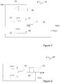
- FIG. 1 illustrates a conventional half bridge converter 10 having input side current sensing by means of a series resistor in series with the high side switch.
- the converter comprises a high side switch S1, and a low side switch S2 connected in series with a half bridge node page be there between.
- the switches are connected across an input voltage Vin, with a sense resistor 12 between the high side switch and the input rail.
- a current sense amplifier, or trans-impedance amplifier, 13 is connected across the sense resistor 12
- An input capacitance Cin is also connected across the input.
- High side switch S1 and low side switch S2 are controlled by means of drivers 14 and 16 respectively.
- On the output side is an inductor 18, connected between the half bridge node HB and the output Vout.
- a output capacitor Cout is also connected across the output.
- Figure 2 illustrates a half bridge converter 20 having a sense resistor in series with the inductor. This converter is similar to that shown in figure 1 , except that the current through the inductor 18 is sensed by means of a sense resistor 22 connected between the inductor 18 and the output Vout, similarly to the sense resistor shown in figure 1 , and a current sense amplifier 23 is connected across the sense resistor.
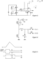
- FIG. 3 shows, in schematic form, an example of a multi-output down converter 30 according to embodiments.
- this converter is a half bridge converter having switches S1 and S2 with a half bridge node of therebetween.
- the current through the inductor 18 may be directed to one or other of two outputs, shown as a first output at 3.3 V, and a second output at 8V.
- the outputs are connected to ground by respective capacitors Cout1 and Cout2.
- the inductor current is routed to the respective outputs by means of first output switch S3 and second output switch S4.
- a separate sense resistor is not included in the circuit; rather a current sense amplifier 33 is connected directly across the switch S3.
- a second sense current amplifier 34 is connected across the second output switch S4.
- the current sense amplifier 33 measures the finite voltage drop across the switch S3, and provided that the switch resistance Rswitch is known, the current through the switch, and thus the current through the inductor 18 (when S3 is closed), can be calculated.
- switch S4 when switch S4 is closed the current sense amplifier 34 measures the finite voltage drop across the switch S4, and provided that the switch resistance Rswitch is known, the current through the switch, and thus the current through the inductor 18 (when S4 is closed), can be calculated.
- a buck converter if a buck converter has more than one output, it will have multiplexing switches, one per output on the output side. Normally only one switch will be closed at a time, directing the inductor current to the output corresponding to that switch. Whenever the switch is closed, the voltage across it will be a measure for the current through it. Thus there is no need for separate sense resistors, and this advantageously may increase efficiency and reduce cost and/or space on the circuit board. Furthermore, since the switches are on the output side of the circuit, they will generally be at a low and DC voltage level so, no specific requirements relating to high-voltage capability is placed on the sense amplifiers, which may thus be lower cost components.
- FIG 4 shows an example of a buck converter 40 operable according to embodiments and figure 5 shows timing diagram of the inductor current and switches of figure 4 .
- the buck converter 40 has an input IN connected across two switches S1 and S2 with a half bridge node therebetween.
- An inductor 18 is connected to the half bridge node, and the output from the inductor is directed towards one or other of two outputs OUT1 one and OUT2 by means of switches S3 and S4 respectively.
- a separate switch S4 which connects the output of the inductor 18 to ground and may be used to avoid ringing, and a bootstrap arrangement of a diode Db and capacitor Cb, connecting a supply voltage Vcc to the half-bridge node in order to generate a floating supply for the high-side switch S1, as will be familiar to the skilled person.
- FIG 5 the timing diagram, for a buck converter 40 as shown in figure 4 operated in discontinuous conduction mode (DCM) is shown.
- the traces show the inductor current 55, the open/closed status of switches S1 and S2 at 51 and 52 respectively, and the open/closed statuses of switches S3 and S4 at 53 and 54.
- S1 When S1 is closed, the inductor current will increase. S1 turns off and S2 turns on, so the inductor current decreases again. When it reaches zero, S3 or S4 can change state. After that, a new cycle can start.
- the inductor current is flowing through either S3 or S4.
- S4a is an optional switch that can be closed if both S3 and S4 are open, to prevent ringing at the right side of the inductor. If S4a is closed, S2 has to be closed as well.
- Figure 6 shows a dual output buck converter according to embodiments.
- switch S3 is implemented as a series connection of diode D3 and NMOS S'3
- switch S4 is implemented as a series connection of diode D4 and NMOS S'4.
- the current sense amplifiers measure the voltage across the switches S'3 and S'4, rather than the respective switch-diode pair D3 + S'3, D4 + S'4.
- Optional switch S4a may be a simple NMOS.
- diode D3 and D4 may be replaced by separates FETs S"3 and S"4, either NMOS or PMOS, to further reduce the losses.
- Figure 7 is otherwise similar to figure 6 .
- diode D3 and D4 are generally required in multiple output buck converters, in order to avoid unintentional currents in the wrong direction.
- the output with the lowest voltage does not require such a diode.
- Power converters employing such switches for current sensing may be used in a wide range of applications, including without limitation solar inverters and uses in automotive fields, as examples of higher voltage applications, and mobile applications such as cell-phones and smart-phones as examples of - typically - lower voltage applications.
Landscapes
- Engineering & Computer Science (AREA)
- Power Engineering (AREA)
- Dc-Dc Converters (AREA)
Claims (6)
- Getakteter Leistungswandler (30), der für einen Betrieb mit einer Mehrzahl von Ausgängen konfiguriert ist und Folgendes aufweist:ein induktives Element (18) undeinen jeweiligen Widerstand für jeden Ausgang in Reihe mit dem induktiven Element, der einen Strom durch das induktive Element bestimmt, wenn der Strom durch das induktive Element zu dem jeweiligen Ausgang geleitet wird,wobei jeder Widerstand ein Widerstand zwischen Hauptanschlüssen eines jeweiligen Schalters in einem eingeschalteten Zustand (53, 54) ist,wobei jeder Schalter zwei Hauptanschlüsse und einen Steueranschluss hat und dazu eingerichtet ist, einen Strom durch das induktive Element zu dem jeweiligen Ausgang der Mehrzahl von Ausgängen zu leiten, undwobei die Schalter an einer Ausgangsseite des getakteten Leistungswandlers sind und derart konfiguriert sind, dass nur ein einziger Schalter zu einer Zeit in dem eingeschalteten Zustand ist.
- Getakteter Leistungswandler gemäß Anspruch 1, wobei jeder Schalter ein Referenzschalter mit relativ geringer Leistung ist, der entweder für einen Betrieb parallel und synchron mit einem Leistungsschalter mit relativ großer Leistung oder als ein Teil eines Leistungsschalters mit relativ hoher Leistung konfiguriert ist.
- Getaktete Stromversorgung gemäß Anspruch 2, wobei jeder Leistungsschalter mit relativ großer Leistung dazu eingerichtet ist, einen Strom durch das induktive Element zu einem der Mehrzahl von Ausgängen zu leiten.
- Getakteter Leistungswandler gemäß einem der vorherigen Ansprüche, des Weiteren mit einem Verstärker (33, 34), der über die Hauptanschlüsse des jeweiligen Schalters angeschlossen ist, um einen Strom durch den Schalter aus der Spannung über den Hauptanschlüssen zu bestimmen.
- Solarwandler mit einem getakteten Leistungswandler gemäß einem der vorherigen Ansprüche.
- Verfahren zum Betreiben einer getakteten Stromversorgung mit einem induktiven Element und einer Mehrzahl von Ausgängen, wobei das Verfahren Folgendes aufweist
Leiten eines Stroms durch das induktive Element zu einem der Mehrzahl von Ausgängen mittels eines jeweiligen Schalters, der zwei Hauptanschlüsse und einen Steueranschluss hat, und
Bestimmen eines Stroms durch das induktive Element durch Messen eines Widerstands in Reihe mit dem induktiven Element,
wobei der Widerstand ein Widerstand zwischen den Hauptanschlüssen des jeweiligen Schalters in einem eingeschalteten Zustand ist,
wobei der Schalter an einer Ausgangsseite des getakteten Leistungswandlers ist und dazu konfiguriert ist, dass nur ein einziger Schalter zu einer Zeit in dem eingeschalteten Zustand ist.
Priority Applications (3)
| Application Number | Priority Date | Filing Date | Title |
|---|---|---|---|
| EP13154564.2A EP2765695B1 (de) | 2013-02-08 | 2013-02-08 | Messstrommessung in Schaltstromwandlern |
| US14/162,627 US9543830B2 (en) | 2013-02-08 | 2014-01-23 | Sense current measurement in switch mode power converters |
| CN201410044872.8A CN104020333B (zh) | 2013-02-08 | 2014-02-07 | 开关式电源转换器中的检测电流的测量 |
Applications Claiming Priority (1)
| Application Number | Priority Date | Filing Date | Title |
|---|---|---|---|
| EP13154564.2A EP2765695B1 (de) | 2013-02-08 | 2013-02-08 | Messstrommessung in Schaltstromwandlern |
Publications (2)
| Publication Number | Publication Date |
|---|---|
| EP2765695A1 EP2765695A1 (de) | 2014-08-13 |
| EP2765695B1 true EP2765695B1 (de) | 2019-10-09 |
Family
ID=47664215
Family Applications (1)
| Application Number | Title | Priority Date | Filing Date |
|---|---|---|---|
| EP13154564.2A Active EP2765695B1 (de) | 2013-02-08 | 2013-02-08 | Messstrommessung in Schaltstromwandlern |
Country Status (3)
| Country | Link |
|---|---|
| US (1) | US9543830B2 (de) |
| EP (1) | EP2765695B1 (de) |
| CN (1) | CN104020333B (de) |
Families Citing this family (4)
| Publication number | Priority date | Publication date | Assignee | Title |
|---|---|---|---|---|
| US9991790B2 (en) * | 2014-06-16 | 2018-06-05 | City University Of Hong Kong | Current control circuit |
| US9755518B2 (en) | 2016-02-05 | 2017-09-05 | Qualcomm Incorporated | Current measurments in switching regulators |
| JP6574743B2 (ja) * | 2016-09-14 | 2019-09-11 | 株式会社東芝 | 電源回路 |
| DE102021203742A1 (de) * | 2021-04-15 | 2022-10-20 | Osram Gmbh | Strommessvorrichtung für getaktete leistungswandler und regelungsschaltung zur anwendung der strommessvorrichtung |
Citations (2)
| Publication number | Priority date | Publication date | Assignee | Title |
|---|---|---|---|---|
| US6222352B1 (en) * | 1999-05-06 | 2001-04-24 | Fairchild Semiconductor Corporation | Multiple voltage output buck converter with a single inductor |
| EP1134880A2 (de) * | 2000-03-17 | 2001-09-19 | Fujitsu Limited | Stromversorgungssteuervorrichtung und -verfahren, Stromversorgungsschaltung und elektronisches Gerät |
Family Cites Families (14)
| Publication number | Priority date | Publication date | Assignee | Title |
|---|---|---|---|---|
| US5414341A (en) * | 1993-12-07 | 1995-05-09 | Benchmarq Microelectronics, Inc. | DC-DC converter operable in an asyncronous or syncronous or linear mode |
| DE69720020D1 (de) * | 1997-12-31 | 2003-04-24 | St Microelectronics Srl | Gleichspannungswandler mit hohem Wirkungsgrad |
| US5982160A (en) | 1998-12-24 | 1999-11-09 | Harris Corporation | DC-to-DC converter with inductor current sensing and related methods |
| JP2001078439A (ja) * | 1999-09-06 | 2001-03-23 | Murata Mfg Co Ltd | スイッチング電源装置 |
| EP1489730A2 (de) * | 2001-05-22 | 2004-12-22 | Powerdsine Limited | Energieverteilung mit digitaler Stromsteuerung |
| US6522110B1 (en) * | 2001-10-23 | 2003-02-18 | Texas Instruments Incorporated | Multiple output switching regulator |
| US20040135562A1 (en) * | 2003-01-13 | 2004-07-15 | Oden Thomas Clark | Single inductor multiple output switchmode power supply |
| US6954054B2 (en) * | 2003-10-17 | 2005-10-11 | International Business Machines Corporation | Total feed forward switching power supply control |
| WO2005074112A1 (en) * | 2004-01-05 | 2005-08-11 | Philips Intellectual Property & Standards Gmbh | Method of operating a dc/dc up/down converter |
| JP2005304210A (ja) * | 2004-04-14 | 2005-10-27 | Renesas Technology Corp | 電源ドライバ装置及びスイッチング電源装置 |
| TW200608708A (en) * | 2004-08-26 | 2006-03-01 | Richtek Techohnology Corp | Current-mode control converter with fixed frequency, and method thereof |
| ITVA20060001A1 (it) | 2006-01-04 | 2007-07-05 | St Microelectronics Srl | Metodo per generare un segnale rappresentativo della corrente erogata ad un carico da un dispositvo di potenza e relativo dispositivo di potenza |
| US7592791B2 (en) * | 2007-08-07 | 2009-09-22 | Newport Media, Inc. | High efficiency DC-DC converter using pulse skipping modulation with programmable burst duration |
| US9479051B2 (en) * | 2011-09-30 | 2016-10-25 | Taiwan Semiconductor Manufacturing Co., Ltd. | Single-inductor multiple-output DC to DC converter |
-
2013
- 2013-02-08 EP EP13154564.2A patent/EP2765695B1/de active Active
-
2014
- 2014-01-23 US US14/162,627 patent/US9543830B2/en active Active
- 2014-02-07 CN CN201410044872.8A patent/CN104020333B/zh active Active
Patent Citations (2)
| Publication number | Priority date | Publication date | Assignee | Title |
|---|---|---|---|---|
| US6222352B1 (en) * | 1999-05-06 | 2001-04-24 | Fairchild Semiconductor Corporation | Multiple voltage output buck converter with a single inductor |
| EP1134880A2 (de) * | 2000-03-17 | 2001-09-19 | Fujitsu Limited | Stromversorgungssteuervorrichtung und -verfahren, Stromversorgungsschaltung und elektronisches Gerät |
Also Published As
| Publication number | Publication date |
|---|---|
| US9543830B2 (en) | 2017-01-10 |
| EP2765695A1 (de) | 2014-08-13 |
| US20140225585A1 (en) | 2014-08-14 |
| CN104020333A (zh) | 2014-09-03 |
| CN104020333B (zh) | 2017-08-01 |
Similar Documents
| Publication | Publication Date | Title |
|---|---|---|
| US9959971B1 (en) | Inductor and converter having the same | |
| US9391518B2 (en) | Current sensing circuit for switching power converters | |
| US11025245B2 (en) | Power conversion device | |
| US9520788B2 (en) | Apparatus and method for current sharing in a multi-phase switching regulator | |
| US9252653B2 (en) | Power factor correction converter and control method thereof | |
| EP2765695B1 (de) | Messstrommessung in Schaltstromwandlern | |
| US9568376B2 (en) | Temperature detecting circuit and method thereof | |
| CN102360234B (zh) | 一种电流控制电路和电流控制方法 | |
| TW200643680A (en) | Buck converter having improved transient response to load step down | |
| US20100181976A1 (en) | Multi-phase driving circuit | |
| US8199540B2 (en) | High voltage gain power converter | |
| CN107408887B (zh) | 用于dc-dc转换器的电流感测控制器 | |
| JP5979252B2 (ja) | 電源装置 | |
| US9337715B2 (en) | Boost converter with first and second modes based upon the input voltage | |
| JP7179657B2 (ja) | 電源回路、及び電源回路の制御方法 | |
| JP6906390B2 (ja) | スイッチング回路 | |
| US10981524B2 (en) | Electronic control unit | |
| JP2017085787A (ja) | 並列チョッパ装置 | |
| US20120286747A1 (en) | Buck converter | |
| US20120286748A1 (en) | Buck converter | |
| CN109586562B (zh) | 多相直流对直流控制器 | |
| US20240235223A1 (en) | Multiport usb fast chargers with fast-charging controller chips including transistor combinations on four chip bases | |
| CN202160110U (zh) | 多相切换式电源供应器以及用于其中的下降讯号产生电路 | |
| JP2018007501A (ja) | 半導体装置 | |
| JP5383397B2 (ja) | 過電圧保護回路 |
Legal Events
| Date | Code | Title | Description |
|---|---|---|---|
| PUAI | Public reference made under article 153(3) epc to a published international application that has entered the european phase |
Free format text: ORIGINAL CODE: 0009012 |
|
| 17P | Request for examination filed |
Effective date: 20131031 |
|
| AK | Designated contracting states |
Kind code of ref document: A1 Designated state(s): AL AT BE BG CH CY CZ DE DK EE ES FI FR GB GR HR HU IE IS IT LI LT LU LV MC MK MT NL NO PL PT RO RS SE SI SK SM TR |
|
| AX | Request for extension of the european patent |
Extension state: BA ME |
|
| RBV | Designated contracting states (corrected) |
Designated state(s): AL AT BE BG CH CY CZ DE DK EE ES FI FR GB GR HR HU IE IS IT LI LT LU LV MC MK MT NL NO PL PT RO RS SE SI SK SM TR |
|
| 17Q | First examination report despatched |
Effective date: 20160922 |
|
| STAA | Information on the status of an ep patent application or granted ep patent |
Free format text: STATUS: EXAMINATION IS IN PROGRESS |
|
| GRAP | Despatch of communication of intention to grant a patent |
Free format text: ORIGINAL CODE: EPIDOSNIGR1 |
|
| STAA | Information on the status of an ep patent application or granted ep patent |
Free format text: STATUS: GRANT OF PATENT IS INTENDED |
|
| RIC1 | Information provided on ipc code assigned before grant |
Ipc: H02M 3/156 20060101AFI20190606BHEP Ipc: G01R 19/165 20060101ALN20190606BHEP Ipc: H02M 1/00 20060101ALN20190606BHEP |
|
| INTG | Intention to grant announced |
Effective date: 20190701 |
|
| GRAS | Grant fee paid |
Free format text: ORIGINAL CODE: EPIDOSNIGR3 |
|
| GRAA | (expected) grant |
Free format text: ORIGINAL CODE: 0009210 |
|
| STAA | Information on the status of an ep patent application or granted ep patent |
Free format text: STATUS: THE PATENT HAS BEEN GRANTED |
|
| AK | Designated contracting states |
Kind code of ref document: B1 Designated state(s): AL AT BE BG CH CY CZ DE DK EE ES FI FR GB GR HR HU IE IS IT LI LT LU LV MC MK MT NL NO PL PT RO RS SE SI SK SM TR |
|
| REG | Reference to a national code |
Ref country code: GB Ref legal event code: FG4D |
|
| REG | Reference to a national code |
Ref country code: CH Ref legal event code: EP |
|
| REG | Reference to a national code |
Ref country code: IE Ref legal event code: FG4D |
|
| REG | Reference to a national code |
Ref country code: DE Ref legal event code: R096 Ref document number: 602013061375 Country of ref document: DE |
|
| REG | Reference to a national code |
Ref country code: AT Ref legal event code: REF Ref document number: 1189984 Country of ref document: AT Kind code of ref document: T Effective date: 20191115 |
|
| REG | Reference to a national code |
Ref country code: NL Ref legal event code: MP Effective date: 20191009 |
|
| REG | Reference to a national code |
Ref country code: LT Ref legal event code: MG4D |
|
| REG | Reference to a national code |
Ref country code: AT Ref legal event code: MK05 Ref document number: 1189984 Country of ref document: AT Kind code of ref document: T Effective date: 20191009 |
|
| PG25 | Lapsed in a contracting state [announced via postgrant information from national office to epo] |
Ref country code: AT Free format text: LAPSE BECAUSE OF FAILURE TO SUBMIT A TRANSLATION OF THE DESCRIPTION OR TO PAY THE FEE WITHIN THE PRESCRIBED TIME-LIMIT Effective date: 20191009 Ref country code: NL Free format text: LAPSE BECAUSE OF FAILURE TO SUBMIT A TRANSLATION OF THE DESCRIPTION OR TO PAY THE FEE WITHIN THE PRESCRIBED TIME-LIMIT Effective date: 20191009 Ref country code: FI Free format text: LAPSE BECAUSE OF FAILURE TO SUBMIT A TRANSLATION OF THE DESCRIPTION OR TO PAY THE FEE WITHIN THE PRESCRIBED TIME-LIMIT Effective date: 20191009 Ref country code: BG Free format text: LAPSE BECAUSE OF FAILURE TO SUBMIT A TRANSLATION OF THE DESCRIPTION OR TO PAY THE FEE WITHIN THE PRESCRIBED TIME-LIMIT Effective date: 20200109 Ref country code: LT Free format text: LAPSE BECAUSE OF FAILURE TO SUBMIT A TRANSLATION OF THE DESCRIPTION OR TO PAY THE FEE WITHIN THE PRESCRIBED TIME-LIMIT Effective date: 20191009 Ref country code: PL Free format text: LAPSE BECAUSE OF FAILURE TO SUBMIT A TRANSLATION OF THE DESCRIPTION OR TO PAY THE FEE WITHIN THE PRESCRIBED TIME-LIMIT Effective date: 20191009 Ref country code: NO Free format text: LAPSE BECAUSE OF FAILURE TO SUBMIT A TRANSLATION OF THE DESCRIPTION OR TO PAY THE FEE WITHIN THE PRESCRIBED TIME-LIMIT Effective date: 20200109 Ref country code: SE Free format text: LAPSE BECAUSE OF FAILURE TO SUBMIT A TRANSLATION OF THE DESCRIPTION OR TO PAY THE FEE WITHIN THE PRESCRIBED TIME-LIMIT Effective date: 20191009 Ref country code: LV Free format text: LAPSE BECAUSE OF FAILURE TO SUBMIT A TRANSLATION OF THE DESCRIPTION OR TO PAY THE FEE WITHIN THE PRESCRIBED TIME-LIMIT Effective date: 20191009 Ref country code: PT Free format text: LAPSE BECAUSE OF FAILURE TO SUBMIT A TRANSLATION OF THE DESCRIPTION OR TO PAY THE FEE WITHIN THE PRESCRIBED TIME-LIMIT Effective date: 20200210 Ref country code: ES Free format text: LAPSE BECAUSE OF FAILURE TO SUBMIT A TRANSLATION OF THE DESCRIPTION OR TO PAY THE FEE WITHIN THE PRESCRIBED TIME-LIMIT Effective date: 20191009 Ref country code: GR Free format text: LAPSE BECAUSE OF FAILURE TO SUBMIT A TRANSLATION OF THE DESCRIPTION OR TO PAY THE FEE WITHIN THE PRESCRIBED TIME-LIMIT Effective date: 20200110 |
|
| PG25 | Lapsed in a contracting state [announced via postgrant information from national office to epo] |
Ref country code: RS Free format text: LAPSE BECAUSE OF FAILURE TO SUBMIT A TRANSLATION OF THE DESCRIPTION OR TO PAY THE FEE WITHIN THE PRESCRIBED TIME-LIMIT Effective date: 20191009 Ref country code: HR Free format text: LAPSE BECAUSE OF FAILURE TO SUBMIT A TRANSLATION OF THE DESCRIPTION OR TO PAY THE FEE WITHIN THE PRESCRIBED TIME-LIMIT Effective date: 20191009 Ref country code: IS Free format text: LAPSE BECAUSE OF FAILURE TO SUBMIT A TRANSLATION OF THE DESCRIPTION OR TO PAY THE FEE WITHIN THE PRESCRIBED TIME-LIMIT Effective date: 20200224 |
|
| PG25 | Lapsed in a contracting state [announced via postgrant information from national office to epo] |
Ref country code: AL Free format text: LAPSE BECAUSE OF FAILURE TO SUBMIT A TRANSLATION OF THE DESCRIPTION OR TO PAY THE FEE WITHIN THE PRESCRIBED TIME-LIMIT Effective date: 20191009 |
|
| REG | Reference to a national code |
Ref country code: DE Ref legal event code: R097 Ref document number: 602013061375 Country of ref document: DE |
|
| PG2D | Information on lapse in contracting state deleted |
Ref country code: IS |
|
| PG25 | Lapsed in a contracting state [announced via postgrant information from national office to epo] |
Ref country code: IS Free format text: LAPSE BECAUSE OF FAILURE TO SUBMIT A TRANSLATION OF THE DESCRIPTION OR TO PAY THE FEE WITHIN THE PRESCRIBED TIME-LIMIT Effective date: 20200209 Ref country code: CZ Free format text: LAPSE BECAUSE OF FAILURE TO SUBMIT A TRANSLATION OF THE DESCRIPTION OR TO PAY THE FEE WITHIN THE PRESCRIBED TIME-LIMIT Effective date: 20191009 Ref country code: EE Free format text: LAPSE BECAUSE OF FAILURE TO SUBMIT A TRANSLATION OF THE DESCRIPTION OR TO PAY THE FEE WITHIN THE PRESCRIBED TIME-LIMIT Effective date: 20191009 Ref country code: DK Free format text: LAPSE BECAUSE OF FAILURE TO SUBMIT A TRANSLATION OF THE DESCRIPTION OR TO PAY THE FEE WITHIN THE PRESCRIBED TIME-LIMIT Effective date: 20191009 Ref country code: RO Free format text: LAPSE BECAUSE OF FAILURE TO SUBMIT A TRANSLATION OF THE DESCRIPTION OR TO PAY THE FEE WITHIN THE PRESCRIBED TIME-LIMIT Effective date: 20191009 |
|
| PLBE | No opposition filed within time limit |
Free format text: ORIGINAL CODE: 0009261 |
|
| STAA | Information on the status of an ep patent application or granted ep patent |
Free format text: STATUS: NO OPPOSITION FILED WITHIN TIME LIMIT |
|
| PG25 | Lapsed in a contracting state [announced via postgrant information from national office to epo] |
Ref country code: SK Free format text: LAPSE BECAUSE OF FAILURE TO SUBMIT A TRANSLATION OF THE DESCRIPTION OR TO PAY THE FEE WITHIN THE PRESCRIBED TIME-LIMIT Effective date: 20191009 Ref country code: IT Free format text: LAPSE BECAUSE OF FAILURE TO SUBMIT A TRANSLATION OF THE DESCRIPTION OR TO PAY THE FEE WITHIN THE PRESCRIBED TIME-LIMIT Effective date: 20191009 Ref country code: SM Free format text: LAPSE BECAUSE OF FAILURE TO SUBMIT A TRANSLATION OF THE DESCRIPTION OR TO PAY THE FEE WITHIN THE PRESCRIBED TIME-LIMIT Effective date: 20191009 |
|
| 26N | No opposition filed |
Effective date: 20200710 |
|
| REG | Reference to a national code |
Ref country code: CH Ref legal event code: PL |
|
| GBPC | Gb: european patent ceased through non-payment of renewal fee |
Effective date: 20200208 |
|
| REG | Reference to a national code |
Ref country code: BE Ref legal event code: MM Effective date: 20200229 |
|
| PG25 | Lapsed in a contracting state [announced via postgrant information from national office to epo] |
Ref country code: LU Free format text: LAPSE BECAUSE OF NON-PAYMENT OF DUE FEES Effective date: 20200208 Ref country code: MC Free format text: LAPSE BECAUSE OF FAILURE TO SUBMIT A TRANSLATION OF THE DESCRIPTION OR TO PAY THE FEE WITHIN THE PRESCRIBED TIME-LIMIT Effective date: 20191009 |
|
| PG25 | Lapsed in a contracting state [announced via postgrant information from national office to epo] |
Ref country code: CH Free format text: LAPSE BECAUSE OF NON-PAYMENT OF DUE FEES Effective date: 20200229 Ref country code: LI Free format text: LAPSE BECAUSE OF NON-PAYMENT OF DUE FEES Effective date: 20200229 Ref country code: SI Free format text: LAPSE BECAUSE OF FAILURE TO SUBMIT A TRANSLATION OF THE DESCRIPTION OR TO PAY THE FEE WITHIN THE PRESCRIBED TIME-LIMIT Effective date: 20191009 |
|
| PG25 | Lapsed in a contracting state [announced via postgrant information from national office to epo] |
Ref country code: IE Free format text: LAPSE BECAUSE OF NON-PAYMENT OF DUE FEES Effective date: 20200208 Ref country code: GB Free format text: LAPSE BECAUSE OF NON-PAYMENT OF DUE FEES Effective date: 20200208 |
|
| PG25 | Lapsed in a contracting state [announced via postgrant information from national office to epo] |
Ref country code: BE Free format text: LAPSE BECAUSE OF NON-PAYMENT OF DUE FEES Effective date: 20200229 |
|
| PG25 | Lapsed in a contracting state [announced via postgrant information from national office to epo] |
Ref country code: TR Free format text: LAPSE BECAUSE OF FAILURE TO SUBMIT A TRANSLATION OF THE DESCRIPTION OR TO PAY THE FEE WITHIN THE PRESCRIBED TIME-LIMIT Effective date: 20191009 Ref country code: MT Free format text: LAPSE BECAUSE OF FAILURE TO SUBMIT A TRANSLATION OF THE DESCRIPTION OR TO PAY THE FEE WITHIN THE PRESCRIBED TIME-LIMIT Effective date: 20191009 Ref country code: CY Free format text: LAPSE BECAUSE OF FAILURE TO SUBMIT A TRANSLATION OF THE DESCRIPTION OR TO PAY THE FEE WITHIN THE PRESCRIBED TIME-LIMIT Effective date: 20191009 |
|
| PG25 | Lapsed in a contracting state [announced via postgrant information from national office to epo] |
Ref country code: MK Free format text: LAPSE BECAUSE OF FAILURE TO SUBMIT A TRANSLATION OF THE DESCRIPTION OR TO PAY THE FEE WITHIN THE PRESCRIBED TIME-LIMIT Effective date: 20191009 |
|
| P01 | Opt-out of the competence of the unified patent court (upc) registered |
Effective date: 20230725 |
|
| PGFP | Annual fee paid to national office [announced via postgrant information from national office to epo] |
Ref country code: DE Payment date: 20240123 Year of fee payment: 12 |
|
| PGFP | Annual fee paid to national office [announced via postgrant information from national office to epo] |
Ref country code: FR Payment date: 20240123 Year of fee payment: 12 |