EP2757094A1 - Carbazole derivative, and light-emitting element, light-emitting device, and electronic device uing carbazole derivative - Google Patents
Carbazole derivative, and light-emitting element, light-emitting device, and electronic device uing carbazole derivative Download PDFInfo
- Publication number
- EP2757094A1 EP2757094A1 EP14001338.4A EP14001338A EP2757094A1 EP 2757094 A1 EP2757094 A1 EP 2757094A1 EP 14001338 A EP14001338 A EP 14001338A EP 2757094 A1 EP2757094 A1 EP 2757094A1
- Authority
- EP
- European Patent Office
- Prior art keywords
- light
- abbreviation
- emitting element
- mixture
- layer
- Prior art date
- Legal status (The legal status is an assumption and is not a legal conclusion. Google has not performed a legal analysis and makes no representation as to the accuracy of the status listed.)
- Withdrawn
Links
- 0 Cc(c(*)c1*)c(*)c(-c2c(*)c(C#N)c(*)c(C)c2*)c1N=O Chemical compound Cc(c(*)c1*)c(*)c(-c2c(*)c(C#N)c(*)c(C)c2*)c1N=O 0.000 description 8
- MAKOZQFGZVKKJN-UHFFFAOYSA-N BrC1C=CC(c(cc2c3c4cccc3)ccc2[n]4-c2ccccc2)=CC1 Chemical compound BrC1C=CC(c(cc2c3c4cccc3)ccc2[n]4-c2ccccc2)=CC1 MAKOZQFGZVKKJN-UHFFFAOYSA-N 0.000 description 1
- NETLULACGKJJII-UHFFFAOYSA-N C(C1)C=CC2=C1C1(c3ccccc3C3C=CC(N(c4ccccc4)c(cc4)ccc4C(C=CC45)=CC4c4ccccc4N5c4ccccc4)=CC13)c1c2cccc1 Chemical compound C(C1)C=CC2=C1C1(c3ccccc3C3C=CC(N(c4ccccc4)c(cc4)ccc4C(C=CC45)=CC4c4ccccc4N5c4ccccc4)=CC13)c1c2cccc1 NETLULACGKJJII-UHFFFAOYSA-N 0.000 description 1
- CVAILDJNGWRDNL-UHFFFAOYSA-N CC1(C)c(cc(cc2)N(c3ccc4-c5ccccc5C(C)(C)c4c3)c(cc3)c(C=CCC4)c4c3-c(cc3)cc(c4ccccc44)c3[n]4-c3ccccc3)c2-c2ccccc12 Chemical compound CC1(C)c(cc(cc2)N(c3ccc4-c5ccccc5C(C)(C)c4c3)c(cc3)c(C=CCC4)c4c3-c(cc3)cc(c4ccccc44)c3[n]4-c3ccccc3)c2-c2ccccc12 CVAILDJNGWRDNL-UHFFFAOYSA-N 0.000 description 1
- UJLBPMDJFVGWGW-UHFFFAOYSA-N CC1(C)c(cc(cc2)N(c3ccccc3)c3cc(-c(cc4)cc(c5ccccc55)c4[n]5-c4ccccc4)ccc3)c2-c2ccccc12 Chemical compound CC1(C)c(cc(cc2)N(c3ccccc3)c3cc(-c(cc4)cc(c5ccccc55)c4[n]5-c4ccccc4)ccc3)c2-c2ccccc12 UJLBPMDJFVGWGW-UHFFFAOYSA-N 0.000 description 1
- QNIGRPLYFFZWRV-UHFFFAOYSA-N CC1(C)c2cc(N(c(cc3)cc(C4(C)C)c3-c3c4cccc3)c(cccc3)c3-c(cc3)cc(c4ccccc44)c3[n]4-c3ccccc3)ccc2-c2ccccc12 Chemical compound CC1(C)c2cc(N(c(cc3)cc(C4(C)C)c3-c3c4cccc3)c(cccc3)c3-c(cc3)cc(c4ccccc44)c3[n]4-c3ccccc3)ccc2-c2ccccc12 QNIGRPLYFFZWRV-UHFFFAOYSA-N 0.000 description 1
- WLYSTOANCHANNF-UHFFFAOYSA-N CC1(C)c2cc(N(c(cc3)cc4c3-c3ccccc3C4(C)C)c(cc3)cc(cc4)c3cc4-c(cc3)cc(c4ccccc44)c3[n]4-c3ccccc3)ccc2-c2c1cccc2 Chemical compound CC1(C)c2cc(N(c(cc3)cc4c3-c3ccccc3C4(C)C)c(cc3)cc(cc4)c3cc4-c(cc3)cc(c4ccccc44)c3[n]4-c3ccccc3)ccc2-c2c1cccc2 WLYSTOANCHANNF-UHFFFAOYSA-N 0.000 description 1
- XUICBWZPKCPCHH-UHFFFAOYSA-N CC1(C)c2cc(N(c3ccccc3)c(ccc3c4)cc3ccc4-c(cc3)cc(c4ccccc44)c3[n]4-c3ccccc3)ccc2-c2c1cccc2 Chemical compound CC1(C)c2cc(N(c3ccccc3)c(ccc3c4)cc3ccc4-c(cc3)cc(c4ccccc44)c3[n]4-c3ccccc3)ccc2-c2c1cccc2 XUICBWZPKCPCHH-UHFFFAOYSA-N 0.000 description 1
- KNIQWVZXZGMYNX-UHFFFAOYSA-N CC1(C)c2cc(N(c3ccccc3)c(cccc3)c3-c(cc3)cc(c4c5cccc4)c3[n]5-c3ccccc3)ccc2-c2ccccc12 Chemical compound CC1(C)c2cc(N(c3ccccc3)c(cccc3)c3-c(cc3)cc(c4c5cccc4)c3[n]5-c3ccccc3)ccc2-c2ccccc12 KNIQWVZXZGMYNX-UHFFFAOYSA-N 0.000 description 1
- JGFBACBKLMLWCJ-UHFFFAOYSA-N CC1(C)c2cc(N(c3ccccc3)c3cccc4c3cccc4-c(cc3)cc(c4c5cccc4)c3[n]5-c3ccccc3)ccc2-c2c1cccc2 Chemical compound CC1(C)c2cc(N(c3ccccc3)c3cccc4c3cccc4-c(cc3)cc(c4c5cccc4)c3[n]5-c3ccccc3)ccc2-c2c1cccc2 JGFBACBKLMLWCJ-UHFFFAOYSA-N 0.000 description 1
- ZHUOKXPWKHFQCT-UHFFFAOYSA-O CC1(C)c2cc([NH+](c(cc3)ccc3-c(cc3)cc(c4ccccc44)c3[n]4-c3ccccc3)c(cc3)cc4c3-c3ccccc3C4(C)C)ccc2-c2c1cccc2 Chemical compound CC1(C)c2cc([NH+](c(cc3)ccc3-c(cc3)cc(c4ccccc44)c3[n]4-c3ccccc3)c(cc3)cc4c3-c3ccccc3C4(C)C)ccc2-c2c1cccc2 ZHUOKXPWKHFQCT-UHFFFAOYSA-O 0.000 description 1
- UJJFRFNTVDTPPZ-UHFFFAOYSA-N CC[n]1c(ccc(-c(cc2C3(C)C)ccc2-c(cc2)c3cc2N(C2(C)C=CC=CC2)c(cc2)ccc2-c2ccccc2)c2)c2c2c1cccc2 Chemical compound CC[n]1c(ccc(-c(cc2C3(C)C)ccc2-c(cc2)c3cc2N(C2(C)C=CC=CC2)c(cc2)ccc2-c2ccccc2)c2)c2c2c1cccc2 UJJFRFNTVDTPPZ-UHFFFAOYSA-N 0.000 description 1
- NJEKHIOHAJHRFH-UHFFFAOYSA-N CC[n]1c(ccc(C(C=CCC23C)=C2C=CC=C3N(c2ccccc2)c(cc2)ccc2-c2ccccc2)c2)c2c2ccccc12 Chemical compound CC[n]1c(ccc(C(C=CCC23C)=C2C=CC=C3N(c2ccccc2)c(cc2)ccc2-c2ccccc2)c2)c2c2ccccc12 NJEKHIOHAJHRFH-UHFFFAOYSA-N 0.000 description 1
- KKKDIMNZZDRPDN-UHFFFAOYSA-N Cc(cc(cc1)-c(cc2)ccc2-c(cc2)cc(c3ccccc33)c2[n]3-c2ccccc2)c1-c(c(C)c1)ccc1-c(cc1)ccc1N(c1ccccc1)c(cc1)ccc1-c1ccccc1 Chemical compound Cc(cc(cc1)-c(cc2)ccc2-c(cc2)cc(c3ccccc33)c2[n]3-c2ccccc2)c1-c(c(C)c1)ccc1-c(cc1)ccc1N(c1ccccc1)c(cc1)ccc1-c1ccccc1 KKKDIMNZZDRPDN-UHFFFAOYSA-N 0.000 description 1
- AKEGIYFOCZBZRC-UHFFFAOYSA-N Cc(cc(cc1)-c(cc2)ccc2-c(cc2)cc(c3ccccc33)c2[n]3-c2ccccc2)c1-c(cc1)c(C)cc1N(c1ccccc1)c(cc1)ccc1-c1ccccc1 Chemical compound Cc(cc(cc1)-c(cc2)ccc2-c(cc2)cc(c3ccccc33)c2[n]3-c2ccccc2)c1-c(cc1)c(C)cc1N(c1ccccc1)c(cc1)ccc1-c1ccccc1 AKEGIYFOCZBZRC-UHFFFAOYSA-N 0.000 description 1
- WXPWZZHELZEVPO-UHFFFAOYSA-N Cc(cc1)ccc1C(c1ccccc1)=O Chemical compound Cc(cc1)ccc1C(c1ccccc1)=O WXPWZZHELZEVPO-UHFFFAOYSA-N 0.000 description 1
- LDCPWRRRGKKRLF-UHFFFAOYSA-N Cc1cc(-c(cc2)cc(c3ccccc33)c2[n]3-c2ccccc2)ccc1-c(cc1)c(C)cc1N(c1ccccc1)c(cc1)ccc1-c1ccccc1 Chemical compound Cc1cc(-c(cc2)cc(c3ccccc33)c2[n]3-c2ccccc2)ccc1-c(cc1)c(C)cc1N(c1ccccc1)c(cc1)ccc1-c1ccccc1 LDCPWRRRGKKRLF-UHFFFAOYSA-N 0.000 description 1
- DKUHPUJMAKJZSD-UHFFFAOYSA-N Cc1cc(N(c2ccccc2)c(cc2)ccc2-c2ccccc2)c(C)cc1-c(cc1)cc(c2c3cccc2)c1[n]3-c1ccccc1 Chemical compound Cc1cc(N(c2ccccc2)c(cc2)ccc2-c2ccccc2)c(C)cc1-c(cc1)cc(c2c3cccc2)c1[n]3-c1ccccc1 DKUHPUJMAKJZSD-UHFFFAOYSA-N 0.000 description 1
- MPECBEYAWUTHRZ-UHFFFAOYSA-N OC1(c(cc(cc2)Br)c2-c2c1cccc2)c1ccccc1-c1ccccc1 Chemical compound OC1(c(cc(cc2)Br)c2-c2c1cccc2)c1ccccc1-c1ccccc1 MPECBEYAWUTHRZ-UHFFFAOYSA-N 0.000 description 1
- DMBHHRLKUKUOEG-UHFFFAOYSA-N c(cc1)ccc1Nc1ccccc1 Chemical compound c(cc1)ccc1Nc1ccccc1 DMBHHRLKUKUOEG-UHFFFAOYSA-N 0.000 description 1
- DMBHHRLKUKUOEG-UHFFFAOYSA-O c(cc1)ccc1[NH2+]c1ccccc1 Chemical compound c(cc1)ccc1[NH2+]c1ccccc1 DMBHHRLKUKUOEG-UHFFFAOYSA-O 0.000 description 1
Images
























Classifications
-
- C—CHEMISTRY; METALLURGY
- C07—ORGANIC CHEMISTRY
- C07D—HETEROCYCLIC COMPOUNDS
- C07D209/00—Heterocyclic compounds containing five-membered rings, condensed with other rings, with one nitrogen atom as the only ring hetero atom
- C07D209/56—Ring systems containing three or more rings
- C07D209/80—[b, c]- or [b, d]-condensed
- C07D209/82—Carbazoles; Hydrogenated carbazoles
- C07D209/86—Carbazoles; Hydrogenated carbazoles with only hydrogen atoms, hydrocarbon or substituted hydrocarbon radicals, directly attached to carbon atoms of the ring system
-
- C—CHEMISTRY; METALLURGY
- C09—DYES; PAINTS; POLISHES; NATURAL RESINS; ADHESIVES; COMPOSITIONS NOT OTHERWISE PROVIDED FOR; APPLICATIONS OF MATERIALS NOT OTHERWISE PROVIDED FOR
- C09K—MATERIALS FOR MISCELLANEOUS APPLICATIONS, NOT PROVIDED FOR ELSEWHERE
- C09K11/00—Luminescent materials, e.g. electroluminescent or chemiluminescent
- C09K11/06—Luminescent materials, e.g. electroluminescent or chemiluminescent containing organic luminescent materials
-
- H—ELECTRICITY
- H10—SEMICONDUCTOR DEVICES; ELECTRIC SOLID-STATE DEVICES NOT OTHERWISE PROVIDED FOR
- H10K—ORGANIC ELECTRIC SOLID-STATE DEVICES
- H10K50/00—Organic light-emitting devices
- H10K50/10—OLEDs or polymer light-emitting diodes [PLED]
- H10K50/14—Carrier transporting layers
- H10K50/15—Hole transporting layers
-
- H—ELECTRICITY
- H10—SEMICONDUCTOR DEVICES; ELECTRIC SOLID-STATE DEVICES NOT OTHERWISE PROVIDED FOR
- H10K—ORGANIC ELECTRIC SOLID-STATE DEVICES
- H10K85/00—Organic materials used in the body or electrodes of devices covered by this subclass
- H10K85/60—Organic compounds having low molecular weight
- H10K85/615—Polycyclic condensed aromatic hydrocarbons, e.g. anthracene
-
- H—ELECTRICITY
- H10—SEMICONDUCTOR DEVICES; ELECTRIC SOLID-STATE DEVICES NOT OTHERWISE PROVIDED FOR
- H10K—ORGANIC ELECTRIC SOLID-STATE DEVICES
- H10K85/00—Organic materials used in the body or electrodes of devices covered by this subclass
- H10K85/60—Organic compounds having low molecular weight
- H10K85/615—Polycyclic condensed aromatic hydrocarbons, e.g. anthracene
- H10K85/624—Polycyclic condensed aromatic hydrocarbons, e.g. anthracene containing six or more rings
-
- H—ELECTRICITY
- H10—SEMICONDUCTOR DEVICES; ELECTRIC SOLID-STATE DEVICES NOT OTHERWISE PROVIDED FOR
- H10K—ORGANIC ELECTRIC SOLID-STATE DEVICES
- H10K85/00—Organic materials used in the body or electrodes of devices covered by this subclass
- H10K85/60—Organic compounds having low molecular weight
- H10K85/631—Amine compounds having at least two aryl rest on at least one amine-nitrogen atom, e.g. triphenylamine
- H10K85/633—Amine compounds having at least two aryl rest on at least one amine-nitrogen atom, e.g. triphenylamine comprising polycyclic condensed aromatic hydrocarbons as substituents on the nitrogen atom
-
- H—ELECTRICITY
- H10—SEMICONDUCTOR DEVICES; ELECTRIC SOLID-STATE DEVICES NOT OTHERWISE PROVIDED FOR
- H10K—ORGANIC ELECTRIC SOLID-STATE DEVICES
- H10K85/00—Organic materials used in the body or electrodes of devices covered by this subclass
- H10K85/60—Organic compounds having low molecular weight
- H10K85/631—Amine compounds having at least two aryl rest on at least one amine-nitrogen atom, e.g. triphenylamine
- H10K85/636—Amine compounds having at least two aryl rest on at least one amine-nitrogen atom, e.g. triphenylamine comprising heteroaromatic hydrocarbons as substituents on the nitrogen atom
-
- H—ELECTRICITY
- H10—SEMICONDUCTOR DEVICES; ELECTRIC SOLID-STATE DEVICES NOT OTHERWISE PROVIDED FOR
- H10K—ORGANIC ELECTRIC SOLID-STATE DEVICES
- H10K85/00—Organic materials used in the body or electrodes of devices covered by this subclass
- H10K85/60—Organic compounds having low molecular weight
- H10K85/649—Aromatic compounds comprising a hetero atom
- H10K85/657—Polycyclic condensed heteroaromatic hydrocarbons
- H10K85/6572—Polycyclic condensed heteroaromatic hydrocarbons comprising only nitrogen in the heteroaromatic polycondensed ring system, e.g. phenanthroline or carbazole
-
- C—CHEMISTRY; METALLURGY
- C09—DYES; PAINTS; POLISHES; NATURAL RESINS; ADHESIVES; COMPOSITIONS NOT OTHERWISE PROVIDED FOR; APPLICATIONS OF MATERIALS NOT OTHERWISE PROVIDED FOR
- C09K—MATERIALS FOR MISCELLANEOUS APPLICATIONS, NOT PROVIDED FOR ELSEWHERE
- C09K2211/00—Chemical nature of organic luminescent or tenebrescent compounds
- C09K2211/10—Non-macromolecular compounds
- C09K2211/1018—Heterocyclic compounds
- C09K2211/1025—Heterocyclic compounds characterised by ligands
- C09K2211/1029—Heterocyclic compounds characterised by ligands containing one nitrogen atom as the heteroatom
Definitions
- the present invention relates to a carbazole derivative, a light-emitting element, a light-emitting device, and an electronic device using a carbazole derivative.
- Such a light-emitting element is a self-luminous type, it has advantages over a liquid crystal display element, such as high visibility of the pixels and no need of backlight and is considered suitable for a flat panel display element.
- a light-emitting element can be manufactured to be thin and light-weight, which is also a great advantage. Further, extremely high response speed is also a feature thereof.
- the light-emitting element described above also has a high utility value as a planar light source which is applicable to lighting or the like.
- Such light-emitting elements using electroluminescence are broadly classified according to whether a light-emitting substance is an organic compound or an inorganic compound.
- a light-emitting substance is an organic compound or an inorganic compound.
- electrons and holes are injected into a layer containing a light-emitting organic compound from a pair of electrodes by applying voltage to a light-emitting element, and then a current flows therethrough. Then, by recombination of these carriers (electrons and holes), the light-emitting organic compound forms an excited state, and emits light when the excited state returns to a ground state.
- an excited state of an organic compound can be a singlet excited state or a triplet excited state.
- Light emission from the singlet excited state is referred to as fluorescence
- light emission from the triplet excited state is referred to as phosphorescence.
- Non-Patent Document 1 Meng-Huan Ho, Yao-Shan Wu and Chin H. Chen, 2005 SID International Symposium Digest of Technical Papers, Vol. XXXVI. pp. 802-805 ).
- NPB N -(1-naphthyl)- N -phenylamino]biphenyl
- NPB has low singlet excitation energy, and there is a possibility that the energy might be transferred from the light-emitting material in the excited state. Since the energy level of an excited state is particularly high in the case of a light-emitting material which emits blue light having a short wavelength, there is a higher possibility that the energy is transferred to NPB. There has been a problem that luminous efficiency of the light-emitting element is lowered due to transfer of the energy to NPB.
- ⁇ 1 , ⁇ 2 , ⁇ 3 , and ⁇ 4 each represent an arylene group having less than or equal to 13 carbon atoms, which forms a ring;
- Ar 1 and Ar 2 each represent an aryl group having less than or equal to 13 carbon atoms, which forms a ring;
- R 1 represents any of a hydrogen atom, an alkyl group having 1 to 6 carbon atoms, a substituted or unsubstituted phenyl group, and a substituted or unsubstituted biphenyl group;
- R 2 represents any of an alkyl group having 1 to 6 carbon atoms, a substituted or unsubstituted phenyl group, and a substituted or unsubstituted biphenyl group.
- l , m, and n are each independent, which is 0 or 1.
- ⁇ 1 to ⁇ 4 in the general formula (1) are represented by any of the following general formulas (2-1) to (2-12).
- R 11 to R 16 , R 21 to R 30 , R 31 to R 38 , and R 41 to R 45 each represent any of a hydrogen atom, an alkyl group having 1 to 6 carbon atoms, a phenyl group, and a biphenyl group.
- R 46 and R 47 each represent any of an alkyl group having 1 to 6 carbon atoms and a phenyl group.
- R 46 and R 47 may be connected to each other to form a ring.
- R 48 represents any of a hydrogen atom, an alkyl group having 1 to 6 carbon atoms, a phenyl group, and a biphenyl group.
- Ar 1 and Ar 2 in the general formula (1) are represented by any of the following general formulas (3-1) to (3-6).
- R 51 to R 56 , R 61 to R 70 , R 71 to R 78 , and R 81 to R 85 each represent any of a hydrogen atom, an alkyl group having 1 to 6 carbon atoms, a phenyl group, and a biphenyl group.
- R 86 and R 87 each represent any of an alkyl group having 1 to 6 carbon atoms and a phenyl group.
- R 86 and R 87 may be connected to each other to form a ring.
- R 88 and R 89 each represent any of a hydrogen atom, an alkyl group having 1 to 6 carbon atoms, a phenyl group, and a biphenyl group.
- R 1 in the general formula (1) is represented by any of the following general formulas (4-1) to (4-9), and R 2 in the general formula (1) is represented by any of the following general formulas (4-2) to (4-9).
- R 51 to R 70 each represent any of a hydrogen atom, an alkyl group having 1 to 6 carbon atoms, a phenyl group, and a biphenyl group.
- one feature of the present invention is represented by any of the following structural formulas (5) to (8).
- a light-emitting element includes an EL layer between a pair of electrodes, the EL layer includes at least a light-emitting layer and a hole-transporting layer, and at least one of the light-emitting layer and the hole-transporting layer contains any of the carbazole derivatives described above.
- a light-emitting element includes an EL layer between an anode and a cathode, the EL layer includes at least a light-emitting layer, a hole-transporting layer, and a hole-injecting layer, the hole-injecting layer is formed in contact with the anode, and at least one of the light-emitting layer, the hole-transporting layer, and the hole-injecting layer contains any of the carbazole derivatives described above.
- the hole-injecting layer contains any of the carbazole derivatives described above and an inorganic compound which exhibits an electron-accepting property with respect to the carbazole derivative.
- an oxide of a transition metal can be used as the inorganic compound.
- the inorganic compound one or more kinds of titanium oxide, vanadium oxide, molybdenum oxide, tungsten oxide, rhenium oxide, ruthenium oxide, chromium oxide, zirconium oxide, hafnium oxide, tantalum oxide, and silver oxide can be used.
- a light-emitting device is formed using any of the light-emitting elements described above, and an electronic device is formed using the light-emitting device.
- the present invention also includes a light-emitting device having the light-emitting element described above and an electronic devuce having the light-emitting device.
- a light-emitting device in this specification refers to an image display device, a light-emitting device, or a light source (including a lighting device).
- light-emitting devices include all of the following modules: modules in which a connector, for example, a flexible printed circuit (FPC), a tape automated bonding (TAB) tape, or a tape carrier package (TCP) is attached to a light-emitting device; modules provided with a printed wiring board at the end of a TAB tape or a TCP; and modules where an integrated circuit (IC) is directly mounted on a light-emitting element by a chip-on-glass (COG) method.
- a connector for example, a flexible printed circuit (FPC), a tape automated bonding (TAB) tape, or a tape carrier package (TCP)
- TAB tape automated bonding
- TCP tape carrier package
- COG chip-on-glass
- the carbazole derivative of the present invention exhibits a high hole-transporting property, it can be mainly used for a hole-transporting layer which is included in an EL layer of a light-emitting element.
- the carbazole derivative of the present invention is used for the hole-transporting layer to form a light-emitting element, whereby a light-emitting element having high luminous efficiency can be formed.
- a light-emitting device and an electronic device which consumes low power and is driven at low voltage can be obtained by using this light-emitting element.
- the carbazole derivative of the present invention is represented by a general formula (1).
- ⁇ 1 , ⁇ 2 , ⁇ 3 , and ⁇ 4 each represent an arylene group having less than or equal to 13 carbon atoms, which forms a ring;
- Ar 1 and Ar 2 each represent an aryl group having less than or equal to 13 carbon atoms, which forms a ring;
- R 1 represents any of a hydrogen atom, an alkyl group having 1 to 6 carbon atoms, a substituted or unsubstituted phenyl group, and a substituted or unsubstituted biphenyl group;
- R 2 represents any of alkyl group having 1 to 6 carbon atoms, a substituted or unsubstituted phenyl group, and a substituted or unsubstituted biphenyl group.
- l , m , and n are each independent, which is 0 or 1.
- ⁇ 1 to ⁇ 4 each represent an arylene group having less than or equal to 13 carbon atoms, which forms a ring.
- substituents represented by structural formulas (2-1) to (2-12) can be given.
- R 11 to R 16 , R 21 to R 30 , R 31 to R 38 , and R 41 to R 45 each represent any of a hydrogen atom, an alkyl group having 1 to 6 carbon atoms, a phenyl group, and a biphenyl group.
- R 46 and R 47 each represent any of an alkyl group having 1 to 6 carbon atoms and a phenyl group.
- R 46 and R 47 may be connected to each other to form a ring.
- R 48 represents any of a hydrogen atom, an alkyl group having 1 to 6 carbon atoms, a phenyl group, and a biphenyl group.
- Ar 1 and Ar 2 each represent an aryl group having less than or equal to 13 carbon atoms, which forms a ring.
- substituents represented by structural formulas (3-1) to (3-6) can be given.
- R 51 to R 56 , R 61 to R 70 , R 71 to R 78 , and R 81 to R 85 each represent any of a hydrogen atom, an alkyl group having 1 to 6 carbon atoms, a phenyl group, and a biphenyl group.
- R 86 and R 87 each represent any of an alkyl group having 1 to 6 carbon atoms and a phenyl group.
- R 86 and R 87 may be connected to each other to form a ring.
- R 88 and R 89 each represent any of a hydrogen atom, an alkyl group having 1 to 6 carbon atoms, a phenyl group, and a biphenyl group.
- R 1 represents any of a hydrogen atom, an alkyl group having 1 to 6 carbon atoms, a substituted or unsubstituted phenyl group, and a substituted or unsubstituted biphenyl group
- R 2 represents any of an alkyl group having 1 to 6 carbon atoms, a substituted or unsubstituted phenyl group, and a substituted or unsubstituted biphenyl group.
- substituents represented by structural formulas (4-1) to (4-9) can be given for R 1
- the substituents represented by the structural formulas (4-2) to (4-9) can be given for R 2 .
- R 51 to R 70 each represent any of a hydrogen atom, an alkyl group having 1 to 6 carbon atoms, a phenyl group, and a biphenyl group.
- carbazole derivatives of the present invention represented by the general formula (1)
- carbazole derivatives represented by structural formulas (9) to (425) can be given.
- the present invention is not limited thereto.
- carbazole derivative of the present invention represented by the general formula (1) can be synthesized by a synthetic method represented by the following synthetic schemes (A-1) to (A-7), a synthetic scheme (B-1), and synthetic schemes (C-1) to (C-2).
- Halogenated secondary arylamine represented by a general formula (compound A) can be synthesized in a manner like the following synthetic scheme (A-1).
- secondary arylamine (compound A 1 ) is halogenated by using a halogenating agent, whereby the halogenated secondary arylamine (compound A) can be obtained.
- the halogenating agent N -bromosuccinimide (NBS), N -iodosuccinimide (NIS), bromine, iodine, potassium iodide, or the like can be used.
- each X 1 represents a halogen group, which is preferably a bromo group or an iodine group.
- a halogenated carbazole derivative represented by a general formula (compound B 2 ) can be synthesized in a manner like the following synthetic scheme (A-2).
- a carbazole derivative (compound B 1 ) is halogenated by using a halogenating agent, whereby the halogenated carbazole derivative (compound B 2 ) can be obtained.
- the halogenating agent N -bromosuccinimide (NBS), N -iodosuccinimide (NIS), bromine, iodine, potassium iodide, or the like can be used.
- each X 1 represents a halogen group, which is preferably a bromo group or an iodine group.
- a compound in which the third position of 9H-carbazole is substituted by boronic acid or organoboron, which is represented by a general formula (compound B), can be synthesized in a manner like the following synthetic scheme (A-3).
- boron oxidation or organoboronation is performed on the halogenated carbazole derivative (compound B 2 ) using an alkyllithium reagent and a boron reagent, whereby the compound in which the third position of 9 H -carbazole is substituted by boronic acid or organoboron (compound B) can be obtained.
- R 99 in the scheme (A-3) represents an alkyl group having 1 to 6 carbon atoms.
- R 98 presents an alkyl group having 1 to 6 carbon atoms.
- R 100 and R 101 each represent a hydrogen atom or an alkyl group having 1 to 6 carbon atoms.
- R 102 and R 103 may be connected to each other to form a ring.
- n -butyllithium, methyllithium, or the like can be used as the alkyllithium reagent.
- Trimethyl borate, isopropyl borate, or the like can be used as the boron reagent.
- Secondary arylamine represented by a general formula (compound C 3 ) can be synthesized in a manner like the following synthetic scheme (A-4). In other words, halogenated aryl (compound C 1 ) and primary arylamine (compound C 2 ) are coupled in the presence of a base using a metal catalyst, whereby the secondary arylamine (compound C 3 ) can be obtained.
- the palladium catalyst which can be used in the synthetic scheme (A-4) although bis(dibenzylideneacetone)palladium(0), palladium(II) acetate, and the like can be given, the palladium catalyst which can be used is not limited thereto.
- the ligand in the palladium catalyst which can be used in the synthetic scheme (A-4) although tri( tert -butyl)phosphine, tri( n -hexyl)phosphine, tricyclohexylphosphine, and the like can be given, the ligand which can be used is not limited thereto.
- a base which can be used in the synthetic scheme (A-4) although an organic base such as sodium tert-butoxide, an inorganic base such as potassium carbonate, and the like can be given, the base which can be used is not limited thereto.
- a solvent that can be used in the synthetic scheme (A-4) although toluene, xylene, benzene, tetrahydrofuran, and the like can be given, the solvent which can be used is not limited thereto.
- R 104 and R 105 each represent a halogen group, an acetyl group, or the like, and chlorine, bromine, and iodine can be given as the halogen group. It is preferable that R 104 be iodine to form copper(I) iodide or that R 105 be an acetyl group to form a copper(II) acetate.
- the copper compound used for the reaction is not limited thereto, and copper can be used as an alternative to the copper compound.
- a base which can be used in the synthetic scheme (A-4) although an inorganic base such as potassium carbonate can be given, the base which can be used is not limited thereto.
- DMPU 1,3-dimethyl-3,4,5,6-tetrahydro-2(1 H )pyrimidinone
- toluene 1,3-dimethyl-3,4,5,6-tetrahydro-2(1 H )pyrimidinone
- xylene 1,3-dimethyl-3,4,5,6-tetrahydro-2(1 H )pyrimidinone
- DMPU or xylene which has a high boiling point is preferably used because, by an Ullmann reaction, an object can be obtained in a shorter time and at a higher yield when the reaction temperature is greater than or equal to 100 °C. Since it is further preferable that the reaction temperature be a temperature greater than or equal to 150 °C, DMPU is more preferably used.
- Tertiary arylamine represented by a general formula (compound C 5 ) can be synthesized in a manner like the following synthetic scheme (A-5).
- the secondary arylamine (compound C 3 ) and halogenated aryl (compound C 4 ) are coupled in the presence of a base using a metal catalyst, whereby the tertiary arylamine (compound C 5 ) can be obtained.
- the palladium catalyst which can be used in the synthetic scheme (A-5) although bis(dibenzylideneacetone)palladium(0), palladium(II) acetate, and the like can be given, the palladium catalyst which can be used is not limited thereto.
- the ligand in the palladium catalyst which can be used in the synthetic scheme (A-5) although tri( tert -butyl)phosphine, tri(n-hexyl)phosphine, tricyclohexylphosphine, and the like can be given, the ligand which can be used is not limited thereto.
- a base which can be used in the synthetic scheme (A-5) although an organic base such as sodium tert -butoxide, an inorganic base such as potassium carbonate, and the like can be given, the base which can be used is not limited thereto.
- a solvent that can be used in the synthetic scheme (A-5) although toluene, xylene, benzene, tetrahydrofuran, and the like can be given, the solvent which can be used is not limited thereto.
- R 104 and R 105 each represent a halogen group, an acetyl group, or the like, and chlorine, bromine, and iodine can be given as the halogen group. It is preferable that R 104 be iodine to form copper(I) iodide or that R 105 be an acetyl group to form a copper(II) acetate.
- the copper compound used for the reaction is not limited thereto, and copper can be used as an alternative to the copper compound.
- a base which can be used in the synthetic scheme (A-5) although an inorganic base such as potassium carbonate can be given, the base which can be used is not limited thereto.
- DMPU 1,3-dimethyl-3,4,5,6-tetrahydro-2(1 H )pyrimidinone
- toluene 1,3-dimethyl-3,4,5,6-tetrahydro-2(1 H )pyrimidinone
- xylene 1,3-dimethyl-3,4,5,6-tetrahydro-2(1 H )pyrimidinone
- benzene 1,3-dimethyl-3,4,5,6-tetrahydro-2(1 H )pyrimidinone
- the solvent which can be used is not limited thereto.
- DMPU or xylene which has a high boiling point is preferably used because, by an Ullmann reaction, an object can be obtained in a shorter time and at a higher yield when the reaction temperature is greater than or equal to 100 °C. Since it is further preferable that the reaction temperature be a temperature greater than or equal to 150 °C, DMPU is more preferably used.
- Tertiary arylamine represented by a general formula (compound C 5 ) can be synthesized in a manner like the following synthetic scheme (A-6).
- the primary arylamine (compound C 2 ) and the halogenated aryl (compounds C 1 and C 4 ) are coupled in the presence of a base using a metal catalyst, whereby the tertiary arylamine (compound C 5 ) can be obtained.
- Ar 1 and Ar 2 are the same, ⁇ 1 and ⁇ 2 are the same, and l and m are the same, the compound C 5 can be obtained with high yield.
- the palladium catalyst which can be used in the synthetic scheme (A-6) although bis(dibenzylideneacetone)palladium(0), palladium(II) acetate, and the like can be given, the palladium catalyst which can be used is not limited thereto.
- the ligand in the palladium catalyst which can be used in the synthetic scheme (A-6) although tri( tert -butyl)phosphine, tri(n-hexyl)phosphine, tricyclohexylphosphine, and the like can be given, the ligand which can be used is not limited thereto.
- a base which can be used in the synthetic scheme (A-6) although an organic base such as sodium tert -butoxide, an inorganic base such as potassium carbonate, and the like can be given, the base which can be used is not limited thereto.
- a solvent that can be used in the synthetic scheme (A-6) although toluene, xylene, benzene, tetrahydrofuran, and the like can be given, the solvent which can be used is not limited thereto.
- R 104 and R 105 each represent a halogen group, an acetyl group, or the like, and chlorine, bromine, and iodine can be given as the halogen group. It is preferable that R 104 be iodine to form copper(I) iodide or that R 105 be an acetyl group to form a copper(II) acetate.
- the copper compound used for the reaction is not limited thereto, and copper can be used as an alternative to the copper compound.
- DMPU 1,3-dimethyl-3,4,5,6-tetrahydro-2(1 H )pyrimidinone
- toluene 1,3-dimethyl-3,4,5,6-tetrahydro-2(1 H )pyrimidinone
- xylene 1,3-dimethyl-3,4,5,6-tetrahydro-2(1 H )pyrimidinone
- benzene 1,3-dimethyl-3,4,5,6-tetrahydro-2(1 H )pyrimidinone
- the solvent which can be used is not limited thereto.
- DMPU or xylene which has a high boiling point is preferably used because, by an Ullmann reaction, an object can be obtained in a shorter time and at a higher yield when the reaction temperature is greater than or equal to 100 °C. Since it is further preferable that the reaction temperature be a temperature greater than or equal to 150 °C, DMPU is more preferably used.
- Halogenated tertiary arylamine represented by a general formula (compound C) can be synthesized in a manner like the following synthetic scheme (A-7).
- tertiary arylamine (compound C 5 ) is halogenated by using a halogenating agent, whereby the halogenated tertiary arylamine (compound C) can be obtained.
- the halogenating agent N -bromosuccinimide (NBS), N -iodosuccinimide (NIS), bromine, iodine, potassium iodide, or the like can be used.
- each X 1 represents a halogen group, which is preferably a bromo group or an iodine group.
- Secondary arylamine having carbazole which is represented by a general formula (compound D), can be synthesized in a manner like the following synthetic scheme (B-1).
- the halogenated secondary arylamine (compound A) and the compound in which the third position of 9H-carbazole is substituted by boronic acid or organoboron (compound B) can be coupled in the presence of a base using a metal catalyst. Accordingly, the secondary arylamine having carbazole (compound D) can be obtained.
- a palladium catalyst which can be used as a metal catalyst palladium(II) acetate, tetrakis(triphenylphosphine)palladium(0), bis(triphenylphosphine)palladium(II)dichloride, and the like can be given.
- a ligand in the above palladium catalyst tri(ortho-tolyl)phosphine, triphenylphosphine, tricyclohexylphosphine, and the like can be given.
- an organic base such as sodium tert -butoxide, an inorganic base such as potassium carbonate, and the like
- a mixed solvent of toluene and water a mixed solvent of toluene, an alcohol such as ethanol, and water; a mixed solvent of xylene and water; a mixed solvent of xylene, an alcohol such as ethanol, and water; a mixed solvent of benzene and water; a mixed solvent of benzene, an alcohol such as ethanol, and water; a mixed solvent of ethers such as ethyleneglycoldimethylether and water; and the like
- a mixed solvent of toluene and water a mixed solvent of toluene, an alcohol such as ethanol, and water
- a mixed solvent of xylene and water a mixed solvent of xylene, an alcohol such as ethanol, and water
- a mixed solvent of benzene and water a mixed solvent of benzene, an alcohol such as ethanol, and water
- the catalyst, ligand, base, and solvent which can be used are not limited thereto.
- cross coupling using organoaluminum, organozirconium, organozinc, or organotin compound, or the like, in addition to arylboronic acid may be employed as a base material.
- organoaluminum, organozirconium, organozinc, or organotin compound, or the like in addition to arylboronic acid, may be employed as a base material.
- the present invention is not limited thereto.
- Tertiary arylamine having carbazole represented by a general formula (compound E) can be synthesized in a manner like the following synthetic scheme (C-1).
- the secondary arylamine having carbazole (compound D) and the halogenated aryl (compound C 4 ) are coupled in the presence of a base using a metal catalyst, whereby the tertiary arylamine having carbazole (compound E), which is a final product, can be obtained.
- a palladium catalyst which can be used as a metal catalyst palladium(II) acetate, tetrakis(triphenylphosphine)palladium(0), bis(triphenylphosphine)palladium(II)dichloride, and the like can be given.
- a ligand in the above palladium catalyst tri(ortho-tolyl)phosphine, triphenylphosphine, tricyclohexylphosphine, and the like can be given.
- an organic base such as sodium tert -butoxide, an inorganic base such as potassium carbonate, and the like
- a mixed solvent of toluene and water a mixed solvent of toluene, an alcohol such as ethanol, and water; a mixed solvent of xylene and water; a mixed solvent of xylene, an alcohol such as ethanol, and water; a mixed solvent of benzene and water; a mixed solvent of benzene, an alcohol such as ethanol, and water; a mixed solvent of ethers such as ethyleneglycoldimethylether and water; and the like
- a mixed solvent of toluene and water a mixed solvent of toluene, an alcohol such as ethanol, and water
- a mixed solvent of xylene and water a mixed solvent of xylene, an alcohol such as ethanol, and water
- a mixed solvent of benzene and water a mixed solvent of benzene, an alcohol such as ethanol, and water
- the catalyst, ligand, base, and solvent which can be used are not limited thereto.
- cross coupling using organoaluminum, organic zirconium, organozinc, organozirconium, organotin, or the like, in addition to arylboronic acid may be employed as a base material.
- the present invention is not limited thereto.
- the tertiary arylamine having carbazole represented by the general formula (compound E) can be synthesized in a manner like the following synthetic scheme (C-2).
- the halogenated tertiary arylamine (compound C) and the compound in which the third position of 9 H -carbazole is substituted by boronic acid or organoboron (compound B) are coupled in the presence of a base using a metal catalyst, whereby the tertiary arylamine having carbazole (compound E), which is a final product, can be obtained.
- Embodiment Mode 2 a light-emitting element which is formed using, for a hole-transporting layer, the carbazole derivative of the present invention described in Embodiment Mode 1 will be described.
- the light-emitting element in Embodiment Mode 2 includes a first electrode which functions as an anode, a second electrode which functions as a cathode, and an EL layer interposed between the first electrode and the second electrode. Note that the light-emitting element in Embodiment Mode 2 can obtain light emission when voltage is applied to each electrode so that the potential of the first electrode is higher than that of the second electrode.
- the EL layer of the light-emitting element in Embodiment Mode 2 includes in its structure a first layer (a hole-injecting layer), a second layer (a hole-transporting layer), a third layer (a light-emitting layer), a fourth layer (an electron-transporting layer), and a fifth layer (an electron-injecting layer), from the first electrode side.
- a structure of the light-emitting element in Embodiment Mode 2 is described with reference to FIGS. 1A and 1B .
- a substrate 101 is used as a support of the light-emitting element.
- glass, quartz, plastics, or the like can be used, for example.
- the substrate 101 may remain in a light-emitting device or an electronic device which is a product utilizing the light-emitting element of the present invention, the substrate 101 may only have a function as the support of the light-emitting element in the manufacturing process of the light-emitting element, without remaining in an end product.
- a metal, an alloy, an electrically conductive compound, a mixture thereof, or the like having a high work function is preferably used.
- a high work function specifically, a work function of 4.0 eV or more
- ITO indium tin oxide
- IZO indium zinc oxide
- indium oxide containing tungsten oxide and zinc oxide is preferably used.
- a first layer 111 in an EL layer 103 which is formed in contact with the first electrode 102 is formed using a composite material with which holes are easily injected regardless of the work function of the first electrode 102.
- an electrode material e.g., a metal, an alloy, an electrically conductive compound, a mixture thereof, or the like, or an element belonging to Group 1 or 2 of the periodic table is also included.
- a film of any of those materials is generally formed by a sputtering method.
- indium zinc oxide (IZO) can be formed by a sputtering method using a target in which 1 wt% to 20 wt% zinc oxide is added to indium oxide; and indium oxide containing tungsten oxide and zinc oxide can be formed by a sputtering method using a target in which 0.5 wt% to 5 wt% tungsten oxide and 0.1 wt% to 1 wt% zinc oxide are added to indium oxide.
- the first layer 111 may be formed by a vacuum evaporation method, an ink-jet method, a spin-coating method, or the like.
- any of a variety of materials such as metals, alloys, and electrically conductive compounds; a mixture thereof; or the like can be used as a substance used for the first electrode 102 regardless of their work functions.
- aluminum (Al), silver (Ag), an alloy containing aluminum (AlSi), or the like can also be used.
- an element belonging to Group 1 or 2 of the periodic table which is a low work function material, that is, an alkali metal such as lithium (Li) or cesium (Cs), an alkaline earth metal such as magnesium (Mg), calcium (Ca), or strontium (Sr), an alloy containing any of these metals (such as an MgAg alloy or an AlLi alloy), a rare-earth metal such as europium (Eu) or ytterbium (Yb), an alloy containing such rare-earth metals, or the like can also be used.
- an alkali metal such as lithium (Li) or cesium (Cs)
- an alkaline earth metal such as magnesium (Mg), calcium (Ca), or strontium (Sr)
- an alloy containing any of these metals such as an MgAg alloy or an AlLi alloy
- a rare-earth metal such as europium (Eu) or ytterbium (Yb)
- the first electrode 102 is formed using an alkali metal, an alkaline-earth metal, or an alloy thereof, a vacuum evaporation method or a sputtering method can be employed.
- a vacuum evaporation method or a sputtering method can be employed in the case of using a silver paste or the like.
- a coating method, an ink-jet method, or the like can be used.
- the EL layer 103 formed over the first electrode 102 a known substance can be used, and any of a low molecular compound and a macromolecular compound can be used. Note that the substance used to form the EL layer 103 has not only a structure formed of only an organic compound but also a structure partially containing an inorganic compound.
- a hole-injecting layer containing a substance having a high hole-injecting property, a hole-transporting layer containing a substance having a high hole-transporting property, a light-emitting layer containing a light-emitting substance, an electron-transporting layer containing a substance having a high electron-transporting property, an electron-injecting layer containing a substance having a high electron-injecting property, and the like are combined with each other and stacked, as appropriate.
- the first layer (a hole-injecting layer) 111, a second layer (a hole-transporting layer) 112, a third layer (a light-emitting layer) 113, a fourth layer (an electron-transporting layer) 114, and a fifth layer (an electron-injecting layer) 115 are sequentially stacked from the first electrode 102 side.
- the first layer 111 which is a hole-injecting layer is a hole-injecting layer containing a substance having a high hole-injecting property.
- a substance having a high hole-injecting property molybdenum oxide, titanium oxide, vanadium oxide, rhenium oxide, ruthenium oxide, chromium oxide, zirconium oxide, hafnium oxide, tantalum oxide, silver oxide, tungsten oxide, manganese oxide, or the like can be used.
- a phthalocyanine-based compound such as phthalocyanine (abbreviation: H 2 Pc), copper(II) phthalocyanine (abbreviation: CuPc), or vanadyl phthalocyanine (abbreviation: VOPc) can be given.
- H 2 Pc phthalocyanine
- CuPc copper(II) phthalocyanine
- VOPc vanadyl phthalocyanine
- aromatic amine compounds which are low-molecular organic compounds can also be given: 4,4',4"-tris( N,N -diphenylamino)triphenylamine (abbreviation: TDATA); 4,4',4"-tris[ N -(3-methylphenyl)- N -phenylamino]triphenylamine (abbreviation: MTDATA); 4,4'-bis[ N -(4-diphenylaminophenyl)- N -phenylamino]biphenyl (abbreviation: DPAB); 4,4'-bis( N - ⁇ 4-[ N '-(3-methylphenyl)- N '-phenylamino]phenyl ⁇ - N -phenylamino)biphenyl (abbreviation: DNTPD); 1,3,5-tris[ N -(4-diphenylaminophenyl)- N -phenylamino]benzene (abbreviation: TDATA
- a macromolecular compound (an oligomer, a dendrimer, a polymer, or the like) can also be used.
- macromolecular compounds such as poly( N -vinylcarbazole) (abbreviation: PVK); poly(4-vinyltriphenylamine) (abbreviation: PVTPA), poly[ N- (4- ⁇ N '-[4-(4-diphenylamino)phenyl]phenyl- N '-phenylamino ⁇ phenyl)methacryla mide] (abbreviation: PTPDMA), and poly[ N,N '-bis(4-butylphenyl)- N,N '-bis(phenyl)benzidine] (abbreviation: Poly-TPD) can be given.
- PVK poly( N -vinylcarbazole)
- PVTPA poly(4-vinyltriphenylamine)
- PTPDMA poly[ N- (4- ⁇ N
- a macromolecular compound, to which acid is added such as poly(3,4-ethylenedioxythiophene)/poly(styrenesulfonic acid) (PEDOT/PSS) or polyaniline/poly(styrenesulfonic acid) (abbreviation: PAni/PSS) can also be used.
- PEDOT/PSS poly(3,4-ethylenedioxythiophene)/poly(styrenesulfonic acid)
- PAni/PSS polyaniline/poly(styrenesulfonic acid)
- the composite material in which a substance having an acceptor property is contained in a substance having a high hole-transporting property can be used.
- a material used to form an electrode may be selected regardless of its work function.
- Such composite materials can be formed by co-evaporation of a substance having a high hole-transporting property and a substance having an acceptor property.
- composition means not only a simple mixture of two materials but also a mixture of a plurality of materials in a condition where an electric charge is given and received among the materials.
- organic compound used for the composite material various compounds such as an aromatic amine compound, a carbazole derivative, aromatic hydrocarbon, and a macromolecular compound (an oligomer, a dendrimer, a polymer, or the like) can be used.
- the organic compound used for the composite material is preferably an organic compound having a high hole-transporting property. Specifically, a substance having a hole mobility of 10 -6 cm 2 /Vs or more is preferably used. However, other than the above substances may be used as long as the substance has a higher hole-transporting property than an electron-transporting property.
- the organic compound that can be used for the composite material is specifically shown below.
- an aromatic amine compound such as MTDATA, TDATA, DPAB, DNTPD, DPA3B, PCzPCA1, PCzPCA2, PCzPCN1, 4,4'-bis[ N -(1-naphthyl)- N -phenylamino]biphenyl (abbreviation: NPB or ⁇ -NPD), and N,N '-bis(3-methylphenyl)- N,N '-diphenyl-[1,1'-biphenyl]-4,4'-diamine (abbreviation: TPD); and a carbazole derivative such as 4,4'-di( N -carbazolyl)biphenyl (abbreviation: CBP), 1,3,5-tris[4-( N -carbazolyl)phenyl]benzene (abbreviation: TCPB), 9-[4-( N -carbazolyl)]phenyl
- NPB or ⁇ -NPD N,
- aromatic hydrocarbon compounds can be given: 2- tert -butyl-9,10-di(2-naphthyl)anthracene (abbreviation: t-BuDNA); 2- tert -butyl-9,10-di(1-naphthyl)anthracene; 9,10-bis(3,5-diphenylphenyl)anthracene (abbreviation: DPPA); 2- tert -butyl-9,10-bis(4-phenylphenyl)anthracene (abbreviation: t-BuDBA); 9,10-di(2-naphthyl)anthracene (abbreviation: DNA); 9,10-diphenylanthracene (abbreviation: DPAnth); 2- tert -butylanthracene (abbreviation: t-BuAnth); 9,10-bis(4-methyl-1-naphthyl)
- aromatic hydrocarbon compound compounds can also be given: 2,3,6,7-tetramethyl-9,10-di(2-naphthyl)anthracene; 9,9'-bianthryl; 10,10'-diphenyl-9,9'-bianthryl; 10,10'-bis(2-phenylphenyl)-9,9'-bianthryl; 10,10'-bis[(2,3,4,5,6-pentaphenyl)phenyl]-9,9'-bianthryl; anthracene; tetracene; rubrene; perylene; 2,5,8,11-tetra( tert -butyl)perylene; pentacene; coronene; 4,4'-bis(2,2-diphenylvinyl)biphenyl (abbreviation: DPVBi); 9,10-bis[4-(2,2-diphenylvinyl)phenyl]anthracene (abbreviation: DPVPA); and the like.
- organic compounds such as 7,7,8,8-tetracyano-2,3,5,6-tetrafluoroquinodimethane (abbreviation: F 4 -TCNQ) and chloranil, and a transition metal oxide can be given.
- oxides of metals belonging to Groups 4 to 8 of the periodic table can be given.
- vanadium oxide, niobium oxide, tantalum oxide, chromium oxide, molybdenum oxide, tungsten oxide, manganese oxide, and rhenium oxide are preferable because of a high electron-accepting property.
- molybdenum oxide is especially preferable because it is stable in the air and its hygroscopic property is low so that it can be easily treated.
- a composite material which is formed using the above macromolecular compound such as PVK, PVTPA, PTPDMA, or Poly-TPD and the above substance having an acceptor property, may be used for the first layer 111.
- a composite material which is formed combining the carbazole derivative of the present invention which is described in Embodiment Mode 1 with the above substance having an acceptor property, can also be used for the first layer 111.
- the second layer 112 which is a hole-transporting layer is a hole-transporting layer containing a substance having a high hole-transporting property. Note that the carbazole derivative of the present invention which is described in Embodiment Mode 1 is used for the second layer 112 in Embodiment Mode 2.
- the carbazole derivative of the present invention which is described in Embodiment Mode 1 can also be used for both the first layer 111 and the second layer 112.
- an element can be manufactured easily and material use efficiency can also be improved.
- energy diagrams of the first layer 111 and the second layer 112 are the same or similar, carriers can be transported easily between the first layer 111 and the second layer 112.
- the third layer 113 is a light-emitting layer containing a substance having a high light-emitting property.
- any of low molecular organic compounds given below can be used.
- N,N '-bis[4-(9 H -carbazol-9-yl)phenyl]- N,N '-diphenylstilbene-4,4'-diamine (abbreviation: YGA2S)
- 4-(9 H -carbazol-9-yl)-4'-(10-phenyl-9-anthryl)triphenylamine (abbreviation: YGAPA), and the like can be given.
- N -(9,10-diphenyl-2-anthryl)- N, 9-diphenyl-9 H -carbazol-3-amine abbreviation: 2PCAPA
- N -[9,10-bis(1,1'-biphenyt-2-yl)-2-anthryl]- N ,9-diphenyl-9 H -carbazol-3-amine abbreviation: 2PCABPhA
- N -(9,10-diphenyl-2-anthryl)- N,N',N'- triphenyl-1,4-phenylenediamine abbreviation: 2DPAPA
- N- [9,10-bis(1,1'-biphenyl-2-yl)-2-anthryl]- N,N',N' -triphenyl-1,4-phenylenediamine abbreviation: 2DPABPhA
- rubrene 5,12-bis(1,1'-biphenyl-4-yi)-6,11-diphenyltetracene (abbreviation: BPT), and the like can be given.
- N,N,N',N' -tetrakis(4-methylphenyl)tetracene-5,11-diamine (abbreviation: p-mPhTD)
- 7,13-diphenyl- N,N,N',N '-tetrakis(4-methylphenyl)acenaphtho[1,2-a]fluoranthene-3,10-d iamine (abbreviation: p-mPhAFD), and the like can be given.
- the third layer 113 may have a structure in which the above substance having a high light-emitting property is dispersed in another substance.
- the concentration of the substance to be dispersed is preferably set 20 % or less of the total in mass ratio.
- a known substance can be used as a substance in which the substance having a light-emitting property is dispersed.
- LUMO level lowest unoccupied molecular orbital level
- HOMO level highest occupied molecular orbital level
- any of the following metal complexes can be used: tris(8-quinolinolato)aluminum(III) (abbreviation: Alq); tris(4-methyl-8-quinolinolato)aluminum(III) (abbreviation: Almq 3 ); bis(10-hydroxybenzo[ h ]quinolinato)beryllium(II) (abbreviation: BeBq 2 ); bis(2-methyl-8-quinolinolato)(4-phenylphenolato)aluminum(III) (abbreviation: BAlq); bis(8-quinolinolato)zinc(II) (abbreviation: Znq); bis[2-(2-benzoxazolyl)phenolato]zinc(II) (abbreviation: ZnPBO); bis[2-(2-benzothiazolyl)phenolato]zinc(II) (abbreviation: ZnBTZ); and the like.
- any of the following heterocyclic compounds can be used: 2-(biphenyl-4-yl)-5-(4- tert -butylphenyl)-1,3,4-oxadiazole (abbreviation: PBD); 1,3-bis[5-( p - tert -butylphenyl)-1,3,4-oxadiazol-2-yl]benzene (abbreviation: OXD-7); 3-(biphenyl-4-yl)-4-phenyl-5-(4- tert -butylphenyl)-1,2,4-triazole (abbreviation: TAZ); 2,2',2"-(1,3,5-benzenetriyl)tris(1-phenyl-1 H -benzimidazole) (abbreviation: TPBI); bathophenanthroline (abbreviation: BPhen); bathocuproine (BCP); and the like.
- PBD 2-(biphenyl-4-yl
- any of the following condensed aromatic compounds can also be used: 9-[4-(10-phenyl-9-anthryl)phenyl]-9 H -Carbazole (abbreviation: CzPA); 3,6-diphenyl-9-[4-(10-phenyl-9-anthryl)phenyl]-9 H -Carbazole (abbreviation: DPCzPA); 9,10-bis(3,5-diphenylphenyl)anthracene (abbreviation: DPPA); 9,10-di(2-naphthyl)anthracene (abbreviation: DNA); 2- tert -butyl-9,10-di(2-naphthyl)anthracene (abbreviation: t-BuDNA); 9,9'-bianthryl (abbreviation: BANT); 9,9'-(stilbene-3,3'-diyl)diphenanthrene (abbreviation: DPNS); 9,9'-(
- the substance in which the substance having a light-emitting property is dispersed a plurality of kinds of substances can be used.
- a substance for suppressing crystallization of rubrene or the like may be further added.
- NPB, Alq, or the like may be further added in order to efficiently transfer energy to the substance having a light-emitting property.
- a substance having an electron-transporting property is preferably used so that the substance having a light-emitting property is dispersed therein to form the third layer 113.
- the following macromolecular compound can be used for the third layer 113.
- poly(9,9-dioctylfluorene-2,7-diyl) (abbreviation: POF)
- poly[(9,9-dioctylfluorene-2,7-diyl)- co -(2,5-dimethoxybenzen-1,4-diyl)] (abbreviation: PF-DMOP)
- poly ⁇ (9,9-dioctylfluorene-2,7-diyl) - co -[ N,N'- di-( p -butylphenyl)-1,4-diaminobenzene] ⁇ (abbreviation: TAB-PFH), and the like can be given.
- poly( p -phenylenvinylene) (abbreviation: PPV)
- poly[(9,9-dihexylfluorene-2,7-diyl)- alt - co -(benzo[2,1,3]thiadiazol-4,7-diyl)] (abbreviation: PFBT)
- poly[(9,9-dioctyl-2,7-divinylenfluorenylene)- alt-co -(2-methoxy-5-(2-ethylhexyloxy)-1, 4-phenylene)] can be given.
- poly[2-methoxy-5-(2'-ethylhexoxy)-1,4-phenylenevinylene] (abbreviation: MEH-PPV), poly(3-butylthiophene-2,5-diyl) (abbreviation: R4-PAT), poly ⁇ [9,9-dihexyl-2,7-bis(1-cyanovinylene)fluorenylene]- alt-co -[2,5-bis( N,N '-diphenyl amino)-1,4-phenylene] ⁇
- poly ⁇ [2-methoxy-5-(2-ethylhexyloxy)-1,4-bis(1-cyanovinylenephenylene)]- alt-co -[2,5-bis( N,N'- diphenylamino)-1,4-phenylene] ⁇ (abbreviation: CN-PPV-DPD), and the like can be given.
- the fourth layer 114 is an electron-transporting layer containing a substance having a high electron-transporting property.
- a metal complex such as Alq, Almq 3 , BeBq 2 , BAlq, Znq, ZnPBO, or ZnBTZ, or the like can be used.
- a heterocyclic compound such as PBD, OXD-7, TAZ, TPBI, BPhen, or BCP can be used.
- the substances described here are mainly substances having an electron mobility of 10 -6 cm 2 /Vs or more.
- the electron-transporting layer is not limited to a single layer but may also be a stack layer of two or more layers formed of the above substances.
- a macromolecular compound can be used for the fourth layer 114.
- a macromolecular compound for the fourth layer 114, a macromolecular compound can be used.
- poly[(9,9-dihexylfluorene-2,7-diyl)- co -(pyridine-3,5-diyl)] abbreviation: PF-Py
- poly[(9,9-dioctylfluorene-2,7-diyl)- co -(2,2'-bipyridine-6,6'-diyl)] abbreviation: PF-BPy
- PF-BPy poly[(9,9-dioctylfluorene-2,7-diyl)- co -(2,2'-bipyridine-6,6'-diyl)]
- the fifth layer 115 is an electron-injecting layer containing a substance having a high electron-injecting property.
- a substance having a high electron-injecting property such as lithium fluoride (LiF), cesium fluoride (CsF), or calcium fluoride (CaF 2 ) can be used.
- a layer formed of a substance having an electron-transporting property which contains an alkali metal, an alkaline earth metal, or a compound thereof, specifically, a layer formed of Alq which contains magnesium (Mg), or the like may be used. Note that in this case, electrons can be more efficiently injected from a second electrode 104.
- a metal, an alloy, an electrically conductive compound, a mixture thereof, or the like having a low work function (specifically, a work function of 3.8 eV or less) can be used.
- a cathode material an element belonging to Group 1 or 2 of the periodic table, that is, an alkali metal such as lithium (Li) or cesium (Cs), an alkaline earth metal such as magnesium (Mg), calcium (Ca), or strontium (Sr), an alloy containing any of these metals (such as an MgAg alloy or an AlLi alloy), a rare-earth metal such as europium (Eu) or ytterbium (Yb), an alloy containing such rare-earth metals, and the like can be given.
- an alkali metal such as lithium (Li) or cesium (Cs)
- an alkaline earth metal such as magnesium (Mg), calcium (Ca), or strontium (Sr)
- an alloy containing any of these metals such as an M
- the second electrode 104 is formed using an alkali metal, an alkaline-earth metal, or an alloy thereof, a vacuum evaporation method or a sputtering method can be employed.
- a vacuum evaporation method or a sputtering method can be employed in the case of using a silver paste or the like.
- a coating method, an ink-jet method, or the like can be used.
- the second electrode 104 can be formed using any of a variety of conductive materials such as Al, Ag, ITO, and indium tin oxide containing silicon or silicon oxide regardless of their work functions. These conductive materials can be formed by a sputtering method, an ink-jet method, a spin coating method, or the like.
- any of a variety of methods can be employed regardless of whether the method is a dry process or a wet process.
- a vacuum evaporation method, an ink-jet method, a spin coating method, or the like can be used. Note that a different formation method may be employed for each layer.
- the second electrode 104 can also be formed by a wet process such as a sol-gel method using a paste of a metal material in addition to a dry process such as a sputtering method or a vacuum evaporation method.
- the light-emitting element of the present invention described above, current flows due to a potential difference generated between the first electrode 102 and the second electrode 104 and holes and electrons recombine in the EL layer 103, whereby light is emitted. Then, this light emission is extracted outside through one of or both the first electrode 102 and the second electrode 104. Therefore, one of or both the first electrode 102 and the second electrode 104 are an electrode having a light-transmitting property.
- the first electrode 102 is an electrode having a light-transmitting property
- light emitted from the EL layer 103 is extracted from the substrate 101 side through the first electrode 102, as shown in FIG 2A .
- the second electrode 104 is an electrode having a light-transmitting property
- light emitted from the EL layer 103 is extracted from the opposite side to the substrate 101 side through the second electrode 104, as shown in FIG 2B .
- first electrode 102 and the second electrode 104 are both electrodes having a light-transmitting property
- light emitted from the EL layer 103 is extracted to both the substrate 101 side and the opposite side to the substrate 101 side, through the first electrode 102 and the second electrode 104, as shown in FIG 2C .
- the structure of the layers provided between the first electrode 102 and the second electrode 104 is not limited to the above. Structures other than the above may be employed as long as at least the second layer 112 which is a hole-transporting layer and the third layer 113 which is a light-emitting layer are included.
- a structure may be employed in which the second electrode 104 which functions as a cathode, the EL layer 103, and the first electrode 102 which functions as an anode are sequentially stacked over the substrate 101.
- the EL layer 103 in this case has a structure in which the fifth layer 115, the fourth layer 114, the third layer 113, the second layer 112, the first layer 111, and the first electrode 102 are sequentially stacked over the second electrode 104.
- a passive matrix light-emitting device or an active matrix light-emitting device in which drive of the light-emitting element is controlled by a thin film transistor (TFT) can be manufactured.
- a staggered TFT or an inverted staggered TFT can be used as appropriate.
- a driver circuit formed over a TFT substrate may be formed of both an n-type TFT and a p-type TFT or only either an n-type TFT or a p-type TFT.
- crystallinity of a semiconductor film used for the TFT Either an amorphous semiconductor film or a crystalline semiconductor film may be used for the TFT.
- the second layer (hole-transporting layer) 112 is formed using the carbazole derivative of the present invention in the light-emitting element which is shown in Embodiment Mode 2, not only improvement in element efficiency but also suppress of increase in drive voltage can be realized.
- Embodiment Mode 2 can be combined with any of the structures described in Embodiment Mode 1 as appropriate.
- Embodiment Mode 3 a light-emitting element having a plurality of EL layers any of the light-emitting elements described in Embodiment Mode 2 (hereinafter referred to as a stacked-type light-emitting element) will be described with reference to FIG 3 .
- This light-emitting element is a stacked-type light-emitting element that has a plurality of EL layers (a first EL layer 303 and a second EL layer 304) between a first electrode 301 and a second electrode 302. Note that although a structure of two EL layers is described in Embodiment Mode 3, a structure of three or more EL layers may also be employed.
- the first electrode 301 functions as an anode
- the second electrode 302 functions as a cathode.
- structures similar to those described in Embodiment Mode 1 can be employed.
- structures similar to those described in Embodiment Mode 2 can be employed.
- structures of the first EL layer 303 and the second EL layer 304 may be the same or different from each other and can be similar to those described in Embodiment Mode 2.
- a charge generation layer 305 is provided between the plurality of EL layers (the first EL layer 303 and the second EL layer 304).
- the charge generation layer 305 has a function of injecting electrons into one of the EL layers and injecting holes into the other of the EL layers when voltage is applied to the first electrode 301 and the second electrode 302.
- the charge generation layer 305 injects electrons into the first EL layer 303 and injects holes into the second EL layer 304.
- the charge generation layer 305 preferably has a light-transmitting property in terms of light extraction efficiency. Further, the charge generation layer 305 functions even when it has lower conductivity than the first electrode 301 or the second electrode 302.
- the charge generation layer 305 may have either a structure in which a substance having an acceptor property is added to a substance having a high hole-transporting property or a structure in which a substance having a donor property is added to a substance having a high electron-transporting property. Alternatively, both of these structures may be stacked.
- an aromatic amine compound such as 4,4'-bis[ N -(1-naphthyl)- N -phenylamino]biphenyl (abbreviation: NPB or ⁇ -NPD), N,N '-bis(3-methylphenyl)- N,N '-diphenyl-[1,1'-biphenyl]-4,4'-diamine (abbreviation: TPD), 4,4',4" -tris( N,N- diphenylamino)triphenylamine (abbreviation: TDATA), 4,4',4"-tris[ N -(3-methylphenyl)- N -phenylamino]triphenylamine (abbreviation: MTDATA), or 4,4'-bis[ N -(spir
- F 4 -TCNQ 7,7,8,8-tetracyano-2,3,5,6-tetrafluoroquinodimethane
- chloranil and the like
- a transition metal oxide can be given.
- oxides of metals belonging to Groups 4 to 8 of the periodic table can be given.
- vanadium oxide, niobium oxide, tantalum oxide, chromium oxide, molybdenum oxide, tungsten oxide, manganese oxide, and rhenium oxide are preferable because of a high electron-accepting property.
- molybdenum oxide is especially preferable because it is stable in the air and its hygroscopic property is low so that it can be easily treated.
- a metal complex having a quinoline skeleton or a benzoquinoline skeleton such as tris(8-quinolinolato)aluminum(III) (abbreviation: Alq), tris(4-methyl-8-quinolinolato)aluminum(III) (abbreviation: Almq 3 ), bis(10-hydroxybenzo[ h ]quinolinato)beryllium(II) (abbreviation: BeBq 2 ), or bis(2-methyl-8-quinolinolato)(4-phenylphenolato)aluminum(III) (abbreviation: BAlq), can be used.
- Alq tris(8-quinolinolato)aluminum(III)
- Almq 3 tris(4-methyl-8-quinolinolato)aluminum(III)
- BeBq 2 bis(10-hydroxybenzo[ h ]quinolinato)beryllium(II)
- BAlq
- a metal complex having an oxazole-based ligand or a thiazole-based ligand such as bis[2-(2'-hydroxyphenyl)benzoxazolato]zinc(II) (abbreviation: Zn(BOX) 2 ) or bis[2-(2'-hydroxyphenyl)benzothiazolato]zinc(II) (abbreviation: Zn(BTZ) 2 ), can also be used.
- any of the following can also be used: 2-(4-biphenylyl)-5-(4-tert-butylphenyl)-1,3,4-oxadiazole (abbreviation: PBD); 1,3-bis[5-( p-tert -butylphenyl)-1,3,4-oxadiazol-2-yl]benzene (abbreviation: OXD-7); 3-(4-biphenylyl)-4-phenyl-5-(4- tert -butylphenyl)-1,2,4-triazole (abbreviation: TAZ); bathophenanthroline (abbreviation: BPhen); bathocuproine (BCP); or the like.
- the substances described here are mainly substances having an electron mobility of 10 -6 cm 2 /Vs or more. Note that other than the above substances may be used as long as the substance has a higher electron-transporting property than a hole-transporting property.
- an alkali metal, an alkaline-earth metal, a rare-earth metal, a metal belonging to Group 13 of the periodic table, or an oxide or carbonate thereof can be used.
- lithium (Li), cesium (Cs), magnesium (Mg), calcium (Ca), ytterbium (Yb), indium (In), lithium oxide, cesium carbonate, or the like is preferably used.
- an organic compound such as tetrathianaphthacene may be used as the substance having a donor property.
- the present invention can be similarly applied to a light-emitting element in which three or more EL layers are stacked.
- a long lifetime element in a high luminance region can be realized while current density is kept low.
- the light-emitting element is applied to lighting as an application example, voltage drop due to resistance of an electrode material can be reduced. Accordingly, light can be uniformly emitted in a large area. Moreover, a light-emitting device which consumes low power and is driven at low voltage can be achieved.
- a desired emission color can be obtained from the whole light-emitting element.
- a light-emitting element emitting white light as a whole light-emitting element can also be obtained.
- complementary color means a relation between colors which becomes an achromatic color when they are mixed. That is, white light emission can be obtained by mixture of lights obtained from substances emitting the lights of complementary colors.
- white light as a whole light-emitting element can be similarly obtained when an emission color of a first EL layer is red, an emission color of a second EL layer is green, and an emission color of a third EL layer is blue.
- Embodiment Mode 3 can be combined with any of the structures described in Embodiment Modes 1 and 2 as appropriate.
- FIG. 4A is a top view of the light-emitting device
- FIG 4B is a cross sectional view taken along A-A' and B-B' in FIG 4A .
- reference numerals 401, 402, and 403 which are shown by a dotted line denote a driver circuit portion (a source driver circuit), a pixel portion, and a driver circuit portion (a gate driver circuit), respectively.
- Reference numerals 404 and 405 denote a sealing substrate and a sealant, respectively, and an inner side region enclosed by the sealant 405 is a space 407.
- a lead wiring 408 is a wiring to transmit a signal to be inputted to the source driver circuit portion 401 and the gate driver circuit 403, and receives a video signal, a clock signal, a start signal, a reset signal, and the like from a flexible printed circuit (FPC) 409 which serves as an external input terminal.
- FPC flexible printed circuit
- this FPC may be provided with a printed wiring board (PWB).
- PWB printed wiring board
- the light-emitting device in this specification includes not only a light-emitting device itself but also a light-emitting device attached with an FPC or a PWB.
- the driver circuit portion and the pixel portion are formed over an element substrate 410.
- one pixel in the pixel portion 402 and the source driver circuit 401 which is the driver circuit portion are shown.
- the source driver circuit 401 a CMOS circuit which is obtained by combining an n-channel TFT 423 and a p-channel TFT 424 is formed.
- the driver circuit may be formed by various CMOS circuits, PMOS circuits, or NMOS circuits.
- Embodiment Mode 4 although a driver-integrated type structure in which a driver circuit is formed over a substrate is described, a driver circuit is not necessarily formed over a substrate but can be formed externally from a substrate.
- the pixel portion 402 is formed of a plurality of pixels having a switching TFT 411, a current control TFT 412, and a first electrode 413 electrically connected to a drain of the current control TFT 412.
- An insulator 414 is formed to cover an end portion of the first electrode 413.
- the insulator 414 is preferably formed so as to have a curved surface with curvature at an upper end portion or a lower end portion thereof in order to obtain favorable coverage.
- the insulator 414 can be formed to have a curved surface with a curvature radius (0.2 ⁇ m to 3 ⁇ m) only at the upper end portion.
- a negative-type photosensitive material which becomes insoluble in an etchant by light irradiation or a positive-type photosensitive material which becomes soluble in an etchant by light irradiation can be used as the insulator 414.
- the first electrode 413 can be formed using any of a variety of materials such as metals, alloys, and electrically conductive compounds, or a mixture thereof. Note that as specific materials, the materials which are shown in Embodiment Mode 2 as a material that can be used for the first electrode can be used.
- the EL layer 416 is formed by any of a variety of methods such as an evaporation method using an evaporation mask, an ink-jet method, or a spin coating method.
- the EL layer 416 has the structure described in Embodiment Mode 2.
- a low molecular compound or a macromolecular compound may be used.
- the material for the EL layer not only an organic compound but also an inorganic compound may also be used.
- the second electrode 417 As a material for the second electrode 417, any of a variety of metals, alloys, and electrically conductive compounds, or a mixture thereof can be used. In the case where the second electrode 417 is used as a cathode, a metal, an alloy, an electrically conductive compound, a mixture thereof, or the like with a low work function (a work function of 3.8 eV or less) is preferably used, among others.
- an element belonging to Group 1 or 2 of the periodic table that is, an alkali metal such as lithium (Li) or cesium (Cs), an alkaline-earth metal such as magnesium (Mg), calcium (Ca), or strontium (Sr), or an alloy containing any of these metals (such as a MgAg alloy or an AlLi alloy); and the like can be given.
- an alkali metal such as lithium (Li) or cesium (Cs)
- an alkaline-earth metal such as magnesium (Mg), calcium (Ca), or strontium (Sr)
- an alloy containing any of these metals such as a MgAg alloy or an AlLi alloy
- a stack of a metal thin film with a reduced thickness and a transparent conductive film indium tin oxide (ITO), indium tin oxide containing silicon or silicon oxide, indium zinc oxide (IZO), or indium oxide containing tungsten oxide and zinc oxide, or the like
- ITO indium tin oxide
- IZO indium zinc oxide
- indium oxide containing tungsten oxide and zinc oxide, or the like can also be used.
- the sealing substrate 404 and the element substrate 410 By attaching the sealing substrate 404 and the element substrate 410 with the sealant 405, there is a structure where a light-emitting element 418 is provided in the space 407 surrounded by the element substrate 410, the sealing substrate 404, and the sealant 405.
- the space 407 is filled with a filler such as an inert gas (e.g ., nitrogen, argon, or the like) or the sealant 405.
- an epoxy-based resin as the sealant 405.
- the material do not transmit moisture and oxygen as much as possible.
- a plastic substrate formed of FRP (Fiberglass-Reinforced Plastics), PVF (polyvinyl fluoride), polyester, acrylic, or the like can be used as well as a glass substrate or a quartz substrate.
- an active matrix light-emitting device having the light-emitting element of the present invention can be obtained.
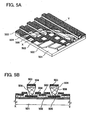
- FIGS. 5A and 5B respectively show a perspective view and a cross-sectional view of a passive matrix light-emitting device using the light-emitting element of the present invention. Note that FIG 5A is a perspective view of the light-emitting device, and FIG 5B is a cross-sectional view of FIG 5A taken along line X-Y.
- an EL layer 504 is provided between a first electrode 502 and a second electrode 503 over a substrate 501.
- An edge portion of the first electrode 502 is covered with an insulating layer 505.
- a partition layer 506 is provided over the insulating layer 505. Sidewalls of the partition layer 506 have a slant such that a distance between one sidewall and the other sidewall becomes narrower as the sidewalls gets closer to a surface of the substrate.
- a cross section of the partition layer 506 in the direction of a short side is trapezoidal, and a lower base (a side facing a similar direction as a plane direction of the insulating layer 505 and in contact with the insulating layer 505) is shorter than an upper base (a side facing a similar direction as the plane direction of the insulating layer 505 and not in contact with the insulating layer 505).
- the passive matrix light-emitting device using the light-emitting element of the present invention can be obtained.
- any of the light-emitting devices described in Embodiment Mode 4 are formed using the light-emitting element of the present invention, which has high luminous efficiency, and accordingly a light-emitting device having reduced power consumption can be obtained.
- Embodiment Mode 4 can be combined with any of the structures described in Embodiment Modes 1 to 3 as appropriate.
- Embodiment Mode 5 an electronic device including, as part thereof, the light-emitting device of the present invention which is shown in Embodiment Mode 4 will be described.
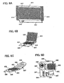
- the electronic device include cameras such as video cameras or digital cameras, goggle type displays, navigation systems, audio reproducing devices (e.g ., car audio systems and audio components), computers, game machines, portable information terminals (e.g ., mobile computers, cellular phones, portable game machines, and electronic books), image reproducing devices in which a recording medium is provided (specifically, devices that are capable of reproducing recording media such as digital versatile discs (DVDs) and equipped with a display unit that can display images), and the like. Specific examples of these electronic devices are shown in FIGS. 6A to 6D .
- FIG. 6A shows a television set according to the present invention, which includes a housing 611, a supporting base 612, a display portion 613, speaker portions 614, video input terminals 615, and the like.
- the light-emitting device of the present invention can be applied to the display portion 613. Since the light-emitting device of the present invention has a feature of high luminous efficiency, a television set having reduced power consumption can be obtained by applying the light-emitting device of the present invention.
- FIG. 6B shows a computer according to the present invention, which includes a main body 621, a housing 622, a display portion 623, a keyboard 624, an external connection port 625, a pointing device 626, and the like.
- the light-emitting device of the present invention can be applied to the display portion 623. Since the light-emitting device of the present invention has a feature of high luminous efficiency, a computer having reduced power consumption can be obtained by applying the light-emitting device of the present invention.
- FIG 6C shows a cellular phone according to the present invention, which includes a main body 631, a housing 632, a display portion 633, an audio input portion 634, an audio output portion 635, operation keys 636, an external connection port 637, an antenna 638, and the like.
- the light-emitting device of the present invention can be applied to the display portion 633. Since the light-emitting device of the present invention has a feature of high luminous efficiency, a cellular phone having reduced power consumption can be obtained by applying the light-emitting device of the present invention.
- FIG 6D shows a camera according to the present invention, which includes a main body 641, a display portion 642, a housing 643, an external connection port 644, a remote control receiving portion 645, an image receiving portion 646, a battery 647, an audio input portion 648, operation keys 649, an eyepiece portion 650, and the like.
- the light-emitting device of the present invention can be applied to the display portion 642. Since the light-emitting device of the present invention has a feature of high luminous efficiency, a camera having reduced power consumption can be obtained by applying the light-emitting device of the present invention.
- the applicable range of the light-emitting device of the present invention is so wide that the light-emitting device can be applied to electronic devices in a variety of fields.
- FIG. 7 is an example of a liquid crystal display device in which the light-emitting device of the present invention is used as a backlight.
- the liquid crystal display device shown in FIG. 7 includes a housing 701, a liquid crystal layer 702, a backlight 703, and a housing 704.
- the liquid crystal layer 702 is connected to a driver IC 705.
- the light-emitting device of the present invention is used for the backlight 703, and current is supplied through a terminal 706.
- the light-emitting device of the present invention as a backlight of a liquid crystal display device as described above, a backlight which consumes low power can be obtained. Further, since the light-emitting device of the present invention is a plane emitting lighting device and the area thereof can be enlarged, the backlight can also have a large area. Therefore, a larger-area liquid crystal display device which consumes low power can be obtained.
- FIG 8 shows an example of using the light-emitting device, to which the present invention is applied, as a table lamp, which is a lighting device.
- a table lamp shown in FIG. 8 has a housing 801 and a light source 802, and the light-emitting device of the present invention is used as the light source 802.
- the light-emitting device of the present invention has the light-emitting element having high luminous efficiency and therefore can be used as a desk lamp which consumes low power.
- FIG 9 shows an example of using the light-emitting device, to which the present invention is applied, as an indoor lighting device 901. Since the area of the light-emitting device of the present invention can also be enlarged, the light-emitting device of the present invention can be used as a lighting device having a large area. In addition, the light-emitting device of the present invention has the light-emitting element having high luminous efficiency and therefore can be used as a lighting device which consumes low power.
- a television set 902 according to the present invention as described in FIG. 6A is placed in a room in which the light-emitting device, to which the present invention is applied, is used as the indoor lighting device 901, public broadcasting and movies can be watched.
- Embodiment Mode 5 can be combined with any of the structures described in Embodiment Modes 1 to 4 as appropriate.
- Embodiment 1 a synthetic method of a carbazole derivative of the present invention, 4-phenyl-4'-(9-phenyl-9 H -carbazol-3-yl)triphenylamine (abbreviation: PCBA1BP) represented by a structural formula (5), will be specifically described.
- PCBA1BP 4-phenyl-4'-(9-phenyl-9 H -carbazol-3-yl)triphenylamine
- NBS N -bromo succinimide
- Step 2-1 A synthetic scheme of 3-bromo-9-phenyl-9H-carbazole in Step 2-1 is shown in the following (D-2-1).
- Step 2-2 A synthetic scheme of 9-phenyl-9H-carbazol-3-boronic acid in Step 2-2 is shown in the following (D-2-2).
- This mixture was refluxed at 100 °C for 10 hours. After the reflux, the aqueous layer of this mixture was extracted with toluene. Then, the extracted solution was combined with an organic layer, followed by washing with a saturated saline solution. After the moisture of the organic layer was removed by magnesium sulfate, this mixture was naturally filtrated, and the obtained filtrate was concentrated to obtain an oily light-brown substance.
- the obtained filtrate was concentrated and purified by silica gel column chromatography.
- a solid which was obtained by concentrating the obtained fraction was recrystallized with a mixture solvent of chloroform and hexane to obtain 2.3 g of a white powder-like solid at a yield of 84 %.
- Sublimation purification of 1.2 g of the obtained white solid was performed by a train sublimation method.
- the sublimation purification was performed under a reduced pressure of 7.0 Pa, with a flow rate of argon at 3 mL/min, at 280 °C for 20 hours. Accordingly, 1.1 g of the white solid was obtained at a yield of 89 %.
- a compound which was obtained through the above Step 4 was measured by a nuclear magnetic resonance method ( 1 H NMR). The measurement result is described below, and the 1 H NMR chart is shown in FIGS. 10A and 10B . It was found from the measurement result that the carbazole derivative of the present invention, 4-phenyl-4'-(9-phenyl-9 H- carbazol-3-yl)triphenylamine (abbreviation: PCBA1BP) represented by the above structural formula (5), was obtained.
- PCBA1BP 4-phenyl-4'-(9-phenyl-9 H- carbazol-3-yl)triphenylamine
- FIG 11A an absorption spectrum of a toluene solution of PCBA1BP (abbreviation) is shown in FIG 11A .
- FIG. 11B an absorption spectrum of a thin film of PCBA1BP (abbreviation) is shown in FIG. 11B .
- An ultraviolet-visible spectrophotometer V-550, manufactured by JASCO Corporation was used for the measurement. The spectrum of the solution was measured in a quartz cell. The sample of the thin film was fabricated by vapor evaporation of PCBA1BP (abbreviation) over a quartz substrate. The absorption spectrum of the solution which was obtained by subtracting the quartz cell from the measured sample is shown in FIG 11A , and the absorption spectrum of the thin film which was obtained by subtracting the quartz substrate from the measured sample is shown in FIG 11B .
- the horizontal axis indicates the wavelength (nm) and the vertical axis indicates the absorption intensity (arbitrary unit).
- an absorption peak was observed at around 335 nm, and in the case of the thin film, an absorption peak was observed at around 341 nm.
- an emission spectrum of the toluene solution (excitation wavelength: 346 nm) of PCBA1BP (abbreviation) is shown in FIG. 11A .
- an emission spectrum of the thin film (excitation wavelength: 386 nm) of PCBA1BP (abbreviation) is shown in FIG 11B .
- the horizontal axis indicates the wavelength (nm) and the vertical axis indicates the light emission intensity (arbitrary unit).
- the maximum emission wavelength was 391 nm (excitation wavelength: 346 nm) in the case of the toluene solution and 416 nm (excitation wavelength: 386 nm) in the case of the thin film.
- PCBA1BP oxidation-reduction reaction characteristic
- CV cyclic voltammetry
- An electrochemical analyzer ALS model 600A or 600C, manufactured by BAS Inc. was used for the measurement.
- DMF dehydrated dimethylformamide
- n -Bu 4 NClO 4 product of Tokyo Chemical Industry Co., Ltd., catalog No. T0836
- the object to be measured was also dissolved in the solvent such that the concentration thereof was 2 mmol/L.
- a platinum electrode (PTE platinum electrode, manufactured by BAS Inc.) was used as a working electrode, another platinum electrode (Pt counter electrode for VC-3 (5 cm), manufactured by BAS Inc.) was used as an auxiliary electrode, and an Ag/Ag + electrode (RE7 reference electrode for nonaqueous solvent, manufactured by BAS Inc.) was used as a reference electrode. Note that the measurement was performed at room temperature (20 °C to 25 °C). In addition, the scan speed at the CV measurement was 0.1 V/sec.
- potential energy (eV) of the reference electrode (Ag/Ag + electrode) used in Embodiment 1 with respect to the vacuum level was calculated. That is, the Fermi level of the Ag/Ag + electrode was calculated. It is known that the oxidation-reduction potential of ferrocene in methanol is +0.610 V [vs. SHE] with respect to a standard hydrogen electrode (Reference: Christian R. Goldsmith et al., J. Am. Chem. Soc., Vol. 124, No. 1, pp.83-96, 2002 ). On the other hand, the oxidation-reduction potential of ferrocene in methanol measured by using the reference electrode used in Embodiment 1 was found to be +0.11 V [vs. Ag/Ag + ]. Therefore, it was found that the potential energy of the reference electrode used in Embodiment 1 was less than that of the standard hydrogen electrode by 0.50 [eV].
- the potential energy of the standard hydrogen electrode with respect to the vacuum level is (-4.44 eV (Reference: Toshihiro Ohnishi and Tamami Koyama, Macromolecular EL material, Kyoritsu Shuppan, pp.64-67 ).
- FIG. 41 shows the CV measurement result on the oxidation reaction characteristics. Note that the measurement of the oxidation reaction characteristics was performed by the steps of scanning the potential of the working electrode with respect to the reference electrode in ranges of (1) 0.07 V to 1.00 V, and then (2) 1.00 V to 0.07 V.
- the oxidation peak took a similar value even after the 100 cycles. Accordingly, it was found that repetition of the oxidation reduction between an oxidation state and a neutral state had favorable chracteristics.
- Embodiment 2 a synthetic method of a carbazole derivative of the present invention, 4,4'-diphenyl-4"-(9-phenyl-9- H -carbazol-3-yl)triphenylamine (abbreviation: PCBBi1BP) represented by a structural formula (6), will be specifically described.
- PCBBi1BP 4,4'-diphenyl-4"-(9-phenyl-9- H -carbazol-3-yl)triphenylamine
- the above obtained toluene layer was combined with the above organic layer, followed by washing with a saturated saline solution. Then, magnesium sulfate was added thereto to remove moisture in the organic layer. Suction filtration was performed on this mixture to concentrate the obtained filtrate.
- the obtained residue was purified by silica gel column chromatography (a developing was solvent: toluene). Accordingly, 13.5 g of a white solid of 4-phenyl-diphenylamine, which was obtained by concentrating the obtained solution, was obtained at a yield of 64 %.
- 4,4'-diphenyltriphenylamine can also be synthesized using a synthetic method shown in Step 1'. Note that a synthetic scheme of 4,4'-diphenyltriphenylamine in Step 1' is shown in the following (E-1').
- Step 1-1 and Step 1-2 which are described above, or 4,4'-diphenyltriphenylamine which was synthesized using a synthetic method shown in Step 1', 4-bromo-4',4"-diphenyltriphenylamine is synthesized. Note that a synthetic scheme of 4-bromo-4',4"-diphenyltriphenylamine in Step 2 is shown in the following (E-2).
- NBS N -bromo succinimide
- a solid which was obtained by concentrating the obtained fraction was recrystallized with a mixture solvent of dichloromethane and hexane to obtain 1.3 g of an objective white solid at a yield of 66 %.
- Sublimation purification of 1.1 g of the obtained white solid was performed by a train sublimation method. The sublimation purification was performed under a reduced pressure of 7.0 Pa, with a flow rate of argon at 4 mL/min, at 305 °C for 15 hours. Accordingly, 840 mg of the white solid was obtained at a yield of 76 %.
- a compound which was obtained through the above Step 4 was measured by a nuclear magnetic resonance method ( 1 H NMR). The measurement result is described below, and the 1 H NMR chart is shown in FIGS. 12A and 12B . It was found from the measurement result that the carbazole derivative of the present invention, 4,4'-diphenyl-4"-(9-phenyl-9- H -carbazol-3-yl)triphenylamine (abbreviation: PCBBi1BP) represented by the above structural formula (6), was obtained.
- PCBBi1BP 4,4'-diphenyl-4"-(9-phenyl-9- H -carbazol-3-yl)triphenylamine
- FIG. 13A an absorption spectrum of a toluene solution of PCBBi1BP (abbreviation) is shown in FIG. 13A .
- FIG. 13B an absorption spectrum of a thin film of PCBBi1BP (abbreviation) is shown in FIG. 13B .
- An ultraviolet-visible spectrophotometer V-550, manufactured by JASCO Corporation was used for the measurement.
- the spectrum of the solution was measured in a quartz cell.
- the sample of the thin film was fabricated by vapor evaporation of PCBBi1BP (abbreviation) over a quartz substrate.
- the absorption spectrum of the solution which was obtained by subtracting the quartz cell from the measured sample is shown in FIG.
- FIG. 13A the absorption spectrum of the thin film which was obtained by subtracting the quartz substrate from the measured sample is shown in FIG. 13B .
- the horizontal axis indicates the wavelength (nm) and the vertical axis indicates the absorption intensity (arbitrary unit).
- an absorption peak was observed at around 347 nm, and in the case of the thin film, an absorption peak was observed at around 350 nm.
- an emission spectrum of the toluene solution (excitation wavelength: 358 nm) of PCBBi1BP (abbreviation) is shown in FIG 13A .
- an emission spectrum of the thin film (excitation wavelength: 366 nm) of PCBBi1BP (abbreviation) is shown FIG 13B .
- the horizontal axis indicates the wavelength (nm) and the vertical axis indicates the light emission intensity (arbitrary unit).
- the maximum emission wavelength was 399 nm (excitation wavelength: 358 nm) in the case of the toluene solution and 417 nm (excitation wavelength: 366 nm) in the case of the thin film.
- PCBBi1BP (abbreviation) was examined by a cyclic voltammetry (CV) measurement. Since the measurement method is similar to that of Embodiment 1, the description is omitted.
- FIG 42 shows the CV measurement result on the oxidation reaction characteristics.
- an oxidization peak potential E pa can be read as 0.521 V
- a reduction peak potential E pc can be read as +0.431 V Therefore, a half-wave potential (an intermediate potential between E pc and E pa ) can be calculated to be +0.48 V.
- the HOMO level of PCBBi1BP abbreviation
- the oxidation peak took a similar value even after the 100 cycles. Accordingly, it was found that repetition of the oxidation reduction between an oxidation state and a neutral state had favorable characteristics.
- PCBBi1BP (abbreviation) was examined with a differential scanning calorimetry (Pyris 1 DSC, manufactured by Perkin Elmer Co., Ltd.). According to the measurement results, it was found that the glass transition temperature was 123 °C. In this manner, PCBBi1BP (abbreviation) has a high glass transition temperature and favorable heat resistance. In addition, the crystallization peak does not exist; thus, it was found that PCBBi1BP (abbreviation) is a substance which is hard to be crystallized.
- Embodiment 3 a synthetic method of a carbazole derivative of the present invention, 9,9-dimethyl- N -phenyl- N -[4-(9-phenyl-9 H -carbazol-3-yl)phenyl]-fluorene-2-amine (abbreviation: PCBAF) represented by a structural formula (7), will be specifically described.
- PCBAF 9,9-dimethyl- N -phenyl- N -[4-(9-phenyl-9 H -carbazol-3-yl)phenyl]-fluorene-2-amine
- This mixture was subjected to suction filtration and concentrated. Then, a residue thereof was purified by silica gel column chromatography.
- Step 2 Synthesis of 9,9-dimethyl- N -phenyl- N -[4-(9-phenyl-9 H -carbazol-3-yl)phenyl]-fluorene-2-amine (abbreviation: PCBAF)]
- PCBA 4-(9-phenyl-9H-carbazol-3-yl)diphenylamine
- the obtained filtrate was concentrated and purified by silica gel column chromatography.
- a solid which was obtained by concentrating the obtained fraction was recrystallized with a mixture solvent of chloroform and hexane to obtain 1.3 g of an objective compound at a yield of 44%.
- Sublimation purification of 1.3 g of the obtained light yellow solid was performed by a train sublimation method.
- the sublimation purification was performed under a reduced pressure of 7.0 Pa, with a flow rate of argon at 3 mL/min, at 270 °C for 20 hours. Accordingly, 1.0 g of the light yellow solid was obtained at a yield of 77 %.
- a compound which was obtained through the above Step 2 was measured by a nuclear magnetic resonance method ( 1 H NMR). The measurement result is described below, and the 1 H NMR chart is shown in FIGS. 14A and 14B . It was found from the measurement result that the carbazole derivative of the present invention, 9,9-dimethyl- N -phenyl- N- [4-(9-phenyl-9 H -carbazol-3-yl)phenyl]-fluorene-2-amine (abbreviation: PCBAF) represented by the above structural formula (7), was obtained.
- PCBAF 9,9-dimethyl- N -phenyl- N- [4-(9-phenyl-9 H -carbazol-3-yl)phenyl]-fluorene-2-amine
- FIG. 15A an absorption spectrum of a toluene solution of PCBAF (abbreviation) is shown in FIG. 15A .
- FIG. 15B an absorption spectrum of a thin film of PCBAF (abbreviation) is shown in FIG 15B .
- An ultraviolet-visible spectrophotometer V-550, manufactured by JASCO Corporation was used for the measurement.
- the spectrum of the solution was measured in a quartz cell.
- the sample of the thin film was fabricated by vapor evaporation of PCBAF (abbreviation) over a quartz substrate.
- the absorption spectrum of the solution which was obtained by subtracting the quartz cell from the measured sample is shown in FIG.
- FIG. 15A the absorption spectrum of the thin film which was obtained by subtracting the quartz substrate from the measured sample is shown in FIG. 15B .
- the horizontal axis indicates the wavelength (nm) and the vertical axis indicates the absorption intensity (arbitrary unit).
- an absorption peak was observed at around 339 nm, and in the case of the thin film, an absorption peak was observed at around 345 nm.
- an emission spectrum of the toluene solution (excitation wavelength: 347 nm) of PCBAF (abbreviation) is shown in FIG 15A .
- FIG 15B an emission spectrum of the thin film (excitation wavelength: 370 nm) of PCBAF (abbreviation) is shown FIG 15B .
- the horizontal axis indicates the wavelength (nm) and the vertical axis indicates the light emission intensity (arbitrary unit).
- the maximum emission wavelength was 394 nm (excitation wavelength: 347 nm) in the case of the toluene solution and 404 nm (excitation wavelength: 370 nm) in the case of the thin film.
- FIG. 43 shows the CV measurement result on the oxidation reaction characteristics.
- an oxidization peak potential E pa can be read as 0.481 V
- a reduction peak potential E pc can be read as +0.393 V. Therefore, a half-wave potential (an intermediate potential between E pc and E pa ) can be calculated to be +0.44 V
- the HOMO level of PCBAF abbreviation
- the oxidation peak took a similar value even after the 100 cycles. Accordingly, it was found that repetition of the oxidation reduction between an oxidation state and a neutral state had favorable characteristics.
- Embodiment 4 a synthetic method of a carbazole derivative of the present invention, N -phenyl- N -[4-(9-phenyl-9 H -carbazol-3-yl)phenyl]-spiro-9,9'-bifluoren-2-amine (abbreviation: PCBASF) represented by a structural formula (8), will be specifically described.
- PCBASF N -phenyl- N -[4-(9-phenyl-9 H -carbazol-3-yl)phenyl]-spiro-9,9'-bifluoren-2-amine
- the obtained aqueous layer was extracted twice with ethyl acetate, and this ethyl acetate solution and the obtained organic layer were washed with a saturated saline solution. After moisture was removed by magnesium sulfate, suction filtration and concentration were performed to obtain 18.76 g of a solid of 9-(biphenyl-2-yl)-2-bromo-9-fluorenol at a yield of 90 %.
- Step 2 Synthesis of N -phenyl- N -[4-(9-phenyl-9 H -carbazol-3-yl)phenyl]-spiro-9,9'-bifluoren-2-amine (abbreviation: PCBASF)]
- Sublimation purification of 2.3 g of the obtained white solid was performed by a train sublimation method.
- the sublimation purification was performed under a reduced pressure of 7.0 Pa, with a flow rate of argon at 3 mL/min, at 310 °C for 20 hours. Accordingly, 1.7 g of the white solid was obtained at a yield of 74 %.
- a compound which was obtained through the above Step 2 was measured by a nuclear magnetic resonance method ( 1 H NMR). The measurement result is described below, and the 1 H NMR chart is shown in FIGS. 16A and 16B . It was found from the measurement result that the carbazole derivative of the present invention, N -phenyl- N -[4-(9-phenyl-9 H -carbazol-3-yl)phenyl]-spiro-9,9'-bifluoren-2-amine (abbreviation: PCBASF) represented by the above structural formula (8), was obtained.
- PCBASF N -phenyl- N -[4-(9-phenyl-9 H -carbazol-3-yl)phenyl]-spiro-9,9'-bifluoren-2-amine
- FIG. 17A an absorption spectrum of a toluene solution of PCBASF (abbreviation) is shown in FIG. 17A .
- FIG. 17B an absorption spectrum of a thin film of PCBASF (abbreviation) is shown in FIG. 17B .
- An ultraviolet-visible spectrophotometer V-550, manufactured by JASCO Corporation was used for the measurement.
- the spectrum of the solution was measured in a quartz cell.
- the sample of the thin film was fabricated by vapor evaporation of PCBASF (abbreviation) over a quartz substrate.
- the absorption spectrum of the solution which was obtained by subtracting the quartz cell from the measured sample is shown in FIG.
- FIG. 17A and the absorption spectrum of the thin film which was obtained by subtracting the quartz substrate from the measured sample is shown in FIG. 17B .
- the horizontal axis indicates the wavelength (nm) and the vertical axis indicates the absorption intensity (arbitrary unit).
- an absorption peak was observed at around 338 nm, and in the case of the thin film, an absorption peak was observed at around 345 nm.
- an emission spectrum of the toluene solution (excitation wavelength: 352 nm) of PCBASF (abbreviation) is shown in FIG. 17A .
- FIG. 17B an emission spectrum of the thin film (excitation wavelength: 371 nm) of PCBASF (abbreviation) is shown FIG. 17B .
- the horizontal axis indicates the wavelength (nm) and the vertical axis indicates the light emission intensity (arbitrary unit).
- the maximum emission wavelength was 396 nm (excitation wavelength: 352 nm) in the case of the toluene solution and 427 nm (excitation wavelength: 371 nm) in the case of the thin film.
- FIG 44 shows the CV measurement result on the oxidation reaction characteristics.
- an oxidization peak potential E pa can be read as 0.52 V
- a reduction peak potential E pc can be read as +0.428 V. Therefore, a half-wave potential (an intermediate potential between E pc and E pa ) can be calculated to be +0.47 V.
- the HOMO level of PCBASF abbreviation
- the oxidation peak took a similar value even after the 100 cycles. Accordingly, it was found that repetition of the oxidation reduction between an oxidation state and a neutral state had favorable characteristics.
- Embodiment 5 a method for manufacturing a light-emitting element 2, a light-emitting element 3, a light-emitting element 4, and a light-emitting element 5, which were formed using carbazole derivatives of the present invention that are synthesized in Embodiments 1 to 4 and measurement results of their element characteristics will be described.
- the light-emitting element 2 was formed using 4-phenyl-4'-(9-phenyl-9 H -carbazol-3-yl)triphenylamine (abbreviation: PCBA1BP), the light-emitting element 3 was formed using 4,4'-diphenyl-4"-(9-phenyl-9- H -carbazol-3-yl)triphenylamine (abbreviation: PCBBi1BP), the light-emitting element 4 was formed using 9,9-dimethyl- N -phenyl- N -[4-(9-phenyl-9 H -carbazol-3-yl)phenyl]-fluorene-2-amine (abbreviation: PCBAF), and the light-emitting element 5 was formed using N -phenyl- N -[4-(9-phenyl-9 H -carbazol-3-yl)phenyl]-spiro-9,9'-bifluoren-2-amine (abbreviation: PCBASF
- each element structure of the light-emitting elements in Embodiment 5 is a structure shown in FIG. 18 , in which a hole-transporting layer 1512 is formed using the above carbazole derivative of the present invention.
- a light-emitting element 1 which is a comparative light-emitting element is formed using 4,4'-bis[ N -(1-naphthyl)- N- phenylamino]biphenyl (abbreviation: NPB) for the hole-transporting layer 1512.
- the light-emitting element 1 was formed over the same substrates as the light-emitting elements 2 to 5, and the light-emitting element 1 was compared to the light-emitting elements 2 to 5.
- a structural formula of an organic compound used in Embodiment 5 is shown below.
- indium tin oxide containing silicon oxide was deposited over a substrate 1501 which is a glass substrate by a sputtering method to form a first electrode 1502.
- the thickness of the first electrode 1502 was set to be 110 nm, and the area was set to be 2 mm ⁇ 2 mm.
- the EL layer 1503 in which a plurality of layers are stacked over the first electrode 1502 was formed.
- the EL layer 1503 has a structure in which a first layer 1511 which is a hole-injecting layer, a second layer 1512 which is a hole-transporting layer, a third layer 1513 which is a light-emitting layer, a fourth layer 1514 which is an electron-transporting layer, and a fifth layer 1515 which is an electron-injecting layer are sequentially stacked.
- the substrate having the first electrode 1502 was fixed to a substrate holder provided in a vacuum evaporation apparatus in such a way that the surface of the first electrode 1502 faced downward, and then the pressure was reduced to about 10 -4 Pa. Then, 4,4'-bis[ N -(1-naphthyl)- N -phenylamino]biphenyl (abbreviation: NPB) and molybdenum(VI) oxide were co-evaporated on the first electrode 1502, whereby the first layer 1511 which is a hole-injecting layer was formed.
- NPB N -(1-naphthyl)- N -phenylamino]biphenyl
- VI molybdenum
- the co-evaporation method is an evaporation method in which evaporation is performed using a plurality of evaporation sources at the same time in one treatment chamber.
- a hole-transporting material was deposited over the first layer 1511 to a thickness of 10 nm by an evaporation method using resistive heating, and the second layer 1512 which is a hole-transporting layer was formed.
- NPB 4,4'-bis[ N -(1-naphthyl)- N -phenylamino]biphenyl
- PCBA1BP 4-phenyl-4'-(9-phenyl-9 H- carbazol-3-yl)triphenylamine
- PCBBi1BP 4,4'-diphenyl-4"-(9-phenyl-9- H -carbazol-3-yl)triphenylamine
- the third layer 1513 which is a light-emitting layer was formed over the second layer 1512 by an evaporation method using resistive heating.
- the third layer 1513 was formed by co-evaporating 9-[4-(10-phenyl-9-anthryl)phenyl]-9 H -carbazole (abbreviation: CzPA) and 4-(10-phenyl-9-anthryl)-4'-(9-phenyl-9 H -carbazol-3-yl)triphenylamine (abbreviation: PCBAPA) to a thickness of 30 nm.
- CzPA 9-[4-(10-phenyl-9-anthryl)phenyl]-9 H -carbazole
- PCBAPA 4-(10-phenyl-9-anthryl)-4'-(9-phenyl-9 H -carbazol-3-yl)triphenylamine
- the evaporation rate was controlled so that the weight ratio of CzPA to PCBAPA could be 1:
- tris(8-quinolinolato)aluminum(III) (abbreviation: Alq) was deposited over the third layer 1513 to be a thickness of 10 nm by an evaporation method using resistive heating.
- the fourth layer 1514 which is an electron-transporting layer was formed by depositing bathophenanthroline (abbreviation: BPhen) over the third layer 1513 to a thickness of 20 nm.
- BPhen bathophenanthroline
- the fifth layer 1515 which is an electron-injecting layer was formed by depositing lithium fluoride (LiF) to a thickness of 1 nm over the fourth layer 1514.
- LiF lithium fluoride
- a second electrode 1504 was formed by depositing aluminum to a thickness of 200 nm by an evaporation method using resistance heating, and the light-emitting elements 1 to 5 were formed.
- the light-emitting elements 1 to 5 obtained through the process described above were put into a glove box with a nitrogen atmosphere so that the light-emitting elements were sealed without being exposed to atmospheric air. After that, the operating characteristics of these light-emitting elements were measured. Note that the measurement was performed at room temperature (an atmosphere kept at 25 °C).
- FIG 19 shows the current density vs. luminance characteristics of the light-emitting elements 1 and 2.
- FIG 20 shows the voltage vs. luminance characteristics of the light-emitting elements 1 and 2.
- FIG 21 shows the luminance vs. current efficiency characteristics of the light-emitting elements 1 and 2.
- FIG 22 shows the voltage vs. current characteristics of the light-emitting elements 1 and 2.
- the luminance and the current value were 1277 cd/m 2 and 0.79 mA, respectively. It was found that the light-emitting element 2 using PCBA1BP (abbreviation) for the second layer 1512 showed higher luminance, even when the light-emitting element 2 was compared to the light-emitting element 1 using NPB for the second layer 1512. Further, it was found that the current efficiency was high with respect to the current density or the luminance.
- FIG. 24 shows the results of a continuous lighting test in which the light-emitting element 2 was continuously lit by constant current driving with the initial luminance set at 1000 cd/m 2 (the vertical axis indicates the relative luminance on the assumption that 1000 cd/m 2 is 100 %). From the results in FIG 24 , the light-emitting element 2 exhibits 92% of the initial luminance even after 160 hours, and was found to have a longer lifetime, as compared to the light-emitting element 1. Thus, a long lifetime light-emitting element can be obtained by applying PCBA1BP (abbreviation) of the present invention.
- PCBA1BP abbreviation
- FIG 25 shows the current density vs. luminance characteristics of the light-emitting elements 1 and 3.
- FIG 26 shows the voltage vs. luminance characteristics of the light-emitting elements 1 and 3.
- FIG 27 shows the luminance vs. current efficiency characteristics of the light-emitting elements 1 and 3.
- FIG 28 shows the voltage vs. current characteristics of the light-emitting elements 1 and 3.
- the luminance and the current value were 1328 cd/m 2 and 0.78 mA, respectively. It was found that the light-emitting element 3 using PCBBi1BP (abbreviation) for the second layer 1512 showed higher luminance, even when the light-emitting element 3 was compared to the light-emitting element 1 using NPB for the second layer 1512. Further, it was found that the current efficiency was high with respect to the current density or the luminance.
- FIG 30 shows the current density vs. luminance characteristics of the light-emitting elements 1 and 4.
- FIG 31 shows the voltage vs. luminance characteristics of the light-emitting elements 1 and 4.
- FIG 32 shows the luminance vs. current efficiency characteristics of the light-emitting elements 1 and 4.
- FIG 33 shows the voltage vs. current characteristics of the light-emitting elements 1 and 4.
- FIG. 35 shows the results of a continuous lighting test in which the light-emitting element 4 was continuously lit by constant current driving with the initial luminance set at 1000 cd/m 2 (the vertical axis indicates the relative luminance on the assumption that 1000 cd/m 2 is 100 %). From the results in FIG 35 , the light-emitting element 4 exhibits 92% of the initial luminance even after 160 hours and was found to have a longer lifetime, as compared to the light-emitting element 1. Thus, a long lifetime light-emitting element can be obtained by applying PCBAF (abbreviation) of the present invention.
- PCBAF abbreviation
- FIG. 36 shows the current density vs. luminance characteristics of the light-emitting elements 1 and 5.
- FIG 37 shows the voltage vs. luminance characteristics of the light-emitting elements 1 and 5.
- FIG 38 shows the luminance vs. current efficiency characteristics of the light-emitting elements 1 and 5.
- FIG 39 shows the voltage vs. current characteristics, of the light-emitting elements 1 and 5.
- the luminance and the current value were 1398 cd/m 2 and 1.11 mA, respectively. It was found that the light-emitting element 5 using PCBASF (abbreviation) for the second layer 1512 showed higher luminance, even when the light-emitting element 5 was compared to the light-emitting element 1 using NPB for the second layer 1512. Further, it was found that the current efficiency was high with respect to the current density or the luminance.
- PCBASF abbreviation
- the light-emitting elements 2 to 5 which were formed using the carbazole derivatives of the present invention exhibited an equivalent level of efficiency to the light-emitting element 1.
- a light-emitting element having high efficiency can be obtained by applying the present invention.
- the light-emitting element 8 will be formed in Embodiment 10 by using a co-evaporation film of NPB and molybdenum(VI) oxide for a hole-injecting layer and using PCBBiNB (abbreviation) for a hole-transporting layer.
- the drive voltage of the light-emitting element 1 was 3.8 V
- the luminance and the current value were 949 cd/m 2 and 0.65 mA, respectively, and the light-emitting element 1 exhibited 64 % of the initial luminance when driven for 1500 hours.
- PCBA1BP (abbreviation) was a favorable material also as a hole-injecting material.
- favorable characteristics can also be obtained by using the co-evaporation film with molybdenum(VI) oxide for the hole-injecting layer.
- the light-emitting element 8 will be formed in Embodiment 10 by using a co-evaporation film of NPB and molybdenum(VI) oxide for a hole-injecting layer and using PCBBiNB (abbreviation) for a hole-transporting layer.
- the drive voltage of the light-emitting element 2 was 3.6 V
- the luminance and the current value were 843 cd/m 2 and 0.53 mA, respectively, and the light-emitting element 2 exhibited 65 % of the initial luminance when driven for 1500 hours.
- PCBA1BP (abbreviation) was a favorable material which can be used for both the first layer 1511 which is a hole-injecting layer and the second layer 1512 which is a hole-transporting layer at the same time. Accordingly, an element could be manufactured easily and material use efficiency could also be improved.
- Embodiment 6 a synthetic method of a carbazole derivative of the present invention, (biphenyl-4-yl)(phenyl)[4'-(9-phenyl-9 H- carbazol-3-yl)biphenyl-4-yl]amine (abbreviation: PCTA1BP) represented by a structural formula (15), will be specifically described.
- Step 2 Synthesis of (biphenyl-4-yl)(phenyl)[4'-(9-phenyl-9 H -carbazol-3-yl)biphenyl-4-yl]amine (abbreviation: PCTA1BP)]
- This mixture was deaerated while being stirred under low pressure, and the atmosphere in the flask was substituted by nitrogen. This mixture was stirred at 90 °C for 5 hours. After the stirring, toluene was added to the reaction mixture, and the mixture was heated at 90 °C.
- this suspension was separated into an organic layer and an aqueous layer. After the separation, the organic layer was washed with a saturated sodium hydrogen carbonate solution and a saturated saline solution. Magnesium sulfate was added to the organic layer, and the organic layer was dried. Suction filtration was performed on this mixture through Celite, alumina, and then Florisil to obtain filtrate. The obtained filtrate was concentrated to obtain a solid. The obtained filtrate was dissolved and purified by silica gel column chromatography.
- a solid which was obtained by concentrating the obtained fraction was dissolved in chloroform and purified by high performance liquid chromatography (HPLC) (developing solvent, chloroform).
- HPLC high performance liquid chromatography
- a solid which was obtained by concentrating the obtained fraction was recrystallized with a mixture solvent of chloroform and hexane to obtain 1.7 g of an objective white solid at a yield of 48 %.
- Sublimation purification of 1.0 g of the obtained white solid was performed by a train sublimation method.
- the sublimation purification was performed under a reduced pressure of 7.0 Pa, with a flow rate of argon at 4 mL/min, at 300 °C for 15 hours to obtain 0.62 g of the white solid at a yield of 62 %.
- PCTA1BP absorption spectrum of PCTA1BP (abbreviation) (measurement range: 200 nm to 800 nm) was measured.
- an absorption peak on a long wavelength side was observed at around 349 nm
- an absorption peak on a long wavelength side was observed at around 357 nm.
- PCTA1BP absorption spectrum of PCTA1BP (abbreviation) (measurement range: 370 nm to 550 nm) was measured.
- a maximum emission wavelength was 405 nm (excitation wavelength: 320 nm)
- a maximum emission wavelength was 420 nm (excitation wavelength: 284 nm). Since the measurement method of an absorption spectrum and an emission spectrum is similar to that of Embodiment 1, the description is omitted.
- PCTA1BP (abbreviation) was examined with a differential scanning calorimetry (Pyris 1 DSC, manufactured by Perkin Elmer Co., Ltd.). According to the measurement results, it was found that the glass transition temperature was 118 °C. In this manner, PCTA1BP (abbreviation) has a high glass transition temperature and favorable heat resistance. In addition, the crystallization peak does not exist; thus, it was found that PCTA1BP (abbreviation) is a substance which is hard to be crystallized.
- Embodiment 7 a synthetic method of a carbazole derivative of the present invention, bis(biphenyl-4-yl)[4'-(9-phenyl-9 H -carbazol-3-yl)biphenyl-4-yl]amine (abbreviation: PCTBi1BP) represented by a structural formula (190), will be specifically described.
- PCTBi1BP bis(biphenyl-4-yl)[4'-(9-phenyl-9 H -carbazol-3-yl)biphenyl-4-yl]amine
- This mixture was deaerated while being stirred under low pressure, and the atmosphere in the flask was substituted by nitrogen. This mixture was stirred at 90 °C for 5 hours. After the stirring, toluene was added to the reaction mixture, and the mixture was heated at 90 °C.
- this suspension was separated into an organic layer and an aqueous layer. After the separation, the organic layer was washed with a saturated sodium hydrogen carbonate solution and a saturated saline solution. Magnesium sulfate was added to the organic layer, and the organic layer was dried. Suction filtration was performed on this mixture through Celite, alumina, and then Florisil to obtain filtrate. The obtained filtrate was concentrated to obtain a solid. The obtained filtrate was dissolved in toluene and purified by silica gel column chromatography. The silica gel column chromatography was performed by using toluene as a developing solvent. A solid which was obtained by concentrating the obtained fraction was recrystallized with a mixture solvent of toluene and hexane to obtain 2.4 g of an objective white solid at a yield of 74 %.
- Sublimation purification of the obtained white solid was performed by a train sublimation method.
- the sublimation purification was performed under a reduced pressure of 7.0 Pa, with a flow rate of argon at 3 mL/min, at 340 °C for 20 hours to obtain 0.70 g of the white solid, the theoretical yield of which is 1.5 g, at a yield of 46%.
- PCTBi1BP absorption spectrum of PCTBi1BP (abbreviation) (measurement range: 200 nm to 800 nm) was measured.
- an absorption peak on a long wavelength side was observed at around 350 nm
- an absorption peak on a long wavelength side was observed at around 357 nm.
- PCTBi1BP (abbreviation) (measurement range: 370 nm to 550 nm)
- a maximum emission wavelength was 410 nm (excitation wavelength: 320 nm)
- a maximum emission wavelength was 447 mm (excitation wavelength: 340 nm). Since the measurement method of an absorption spectrum and an emission spectrum is similar to that of Embodiment 1, the description is omitted.
- PCTBi1BP (abbreviation) was examined by a cyclic voltammetry (CV) measurement. Since the measurement method is similar to that of Embodiment 1, the description is omitted.
- the oxidation peak took a similar value even after the 100 cycles. Accordingly, it was found that repetition of the oxidation reduction between an oxidation state and a neutral state had favorable characteristics.
- PCTBi1BP (abbreviation) was examined with a differential scanning calorimetry (Pyris 1 DSC, manufactured by Perkin Elmer Co., Ltd.). According to the measurement results, it was found that the glass transition temperature was 133 °C. In this manner, PCTBi1BP (abbreviation) has a high glass transition temperature and favorable heat resistance. In addition, the crystallization peak does not exist; thus, it was found that PCTBi1BP (abbreviation) is a substance which is hard to be crystallized.
- Embodiment 8 a synthetic method of a carbazole derivative of the present invention, 4-(1-naphthyl)-4'-(9-phenyl-9 H- carbazol-3-yl)-triphenylamine (abbreviation: PCBANB) represented by a structural formula (343), will be specifically described.
- PCBANB 4-(1-naphthyl)-4'-(9-phenyl-9 H- carbazol-3-yl)-triphenylamine
- the obtained oily substance was dissolved in about 20 mL of toluene, and suction filtration was performed on this solution through Celite, alumina, and then Florisil.
- PCBANB absorption spectrum of PCBANB (abbreviation) (measurement range: 200 nm to 800 nm) was measured.
- an absorption peak on a long wavelength side was observed at around 335 nm
- an absorption peak on a long wavelength side was observed at around 341 nm.
- PCBANB abbreviation
- a maximum emission wavelength was 410 nm (excitation wavelength: 345 nm)
- a maximum emission wavelength was 433 nm (excitation wavelength: 341 nm).
- the oxidation peak took a similar value even after the 100 cycles. Accordingly, it was found that repetition of the oxidation reduction between an oxidation state and a neutral state had favorable characteristics.
- PCBANB (abbreviation) was examined with a differential scanning calorimetry (Pyris 1 DSC, manufactured by Perkin Elmer Co., Ltd.). According to the measurement results, it was found that the glass transition temperature was 115 °C. In this manner, PCBANB (abbreviation) has a high glass transition temperature and favorable heat resistance. In addition, the crystallization peak does not exist; thus, it was found that PCBANB (abbreviation) is a substance which is hard to be crystallized.
- FIGS. 56 to 59 show the measurement results in element characteristics of the light-emitting element 6 which was formed using, for a hole-transporting layer, PCBANB (abbreviation) which is the carbazole derivative of the present invention that was synthesized in Embodiment 8 in a manner similar to that of Embodiment 5. It was found that the hole-transporting material of the present invention which was used for the light-emitting element 6 showed higher luminance, even when the hole-transporting material of the present invention which was used for the light-emitting element 6 was compared to NPB of the light-emitting element 1.
- PCBANB abbreviation
- the light-emitting element 1 which is a comparative light-emitting element was formed using 4,4'-bis[ N -(1-naphthyl)- N -phenylamino]biphenyl (abbreviation: NPB) for the hole-transporting layer 151 in a manner similar to that of Embodiment 5.
- NPB 4,4'-bis[ N -(1-naphthyl)- N -phenylamino]biphenyl
- the hole-transporting material of the present invention realizes favorable carrier balance in the structure of the light-emitting element 6.
- FIG 60 shows the result of a continuous lighting test in which the light-emitting element 6 was continuously lit by constant current driving with the initial luminance set at 1000 cd/m 2 (the vertical axis indicates the relative luminance on the assumption that 1000 cd/m 2 is 100 %). From the results in FIG 60 , the light-emitting element 6 was found to have a longer lifetime, as compared to the light-emitting element 1. Thus, a long lifetime light-emitting element can be obtained by applying the present invention.
- Embodiment 9 a synthetic method of a carbazole derivative of the present invention, 4,4'-di(1-naphthyl)-4"-(9-phenyl-9 H -carbazol-3-yl)-triphenylamine (abbreviation: PCBNBB) represented by a structural formula (229), will be specifically described.
- PCBNBB 4,4'-di(1-naphthyl)-4"-(9-phenyl-9 H -carbazol-3-yl)-triphenylamine
- NBS N-bromo succinimide
- NBS N -bromo succinimide
- PCBNBB absorption spectrum of PCBNBB (abbreviation) (measurement range: 200 nm to 800 nm) was measured.
- PCBNBB absorption peak on a long wavelength side
- an absorption peak on a long wavelength side was observed at around 345 nm
- an absorption peak on a long wavelength side was observed at around 355 nm.
- PCBNBB abbreviation
- a maximum emission wavelength was 413 nm (excitation wavelength: 355 nm)
- a maximum emission wavelength was 428 nm (excitation wavelength: 370 nm).
- PCBNBB abbreviation
- a differential scanning calorimetry Puls 1 DSC, manufactured by Perkin Elmer Co., Ltd.
- the glass transition temperature was 136 °C.
- PCBNBB abbreviation
- the crystallization peak does not exist; thus, it was found that PCBNBB (abbreviation) is a substance which is hard to be crystallized.
- FIGS. 56 to 59 show the measurement results in element characteristics of the light-emitting element 7 which was formed using, for a hole-transporting layer, PCBNBB (abbreviation) which is the carbazole derivative of the present invention that was synthesized in Embodiment 9 in a manner similar to that of Embodiment 5. It was found that the hole-transporting material of the present invention which was used for the light-emitting element 7 showed higher luminance, even when the hole-transporting material of the present invention which was used for the light-emitting element 7 was compared to NPB of the light-emitting element 1.
- PCBNBB abbreviation
- the light-emitting element 1 which is a comparative light-emitting element was formed using 4,4'-bis[ N -(1-naphthyl)- N -phenylaminolbiphenyl (abbreviation: NPB) for the hole-transporting layer 151 in a manner similar to that of Embodiment 5.
- NPB 4,4'-bis[ N -(1-naphthyl)- N -phenylaminolbiphenyl
- the hole-transporting material of the present invention realizes favorable carrier balance in the structure of the light-emitting element 7.
- FIG 60 shows the result of a continuous lighting test in which the light-emitting element 7 was continuously lit by constant current driving with the initial luminance set at 1000 cd/m 2 (the vertical axis indicates the relative luminance on the assumption that 1000 cd/m 2 is 100 %). From the results in FIG 60 , the light-emitting element 7 was found to have a longer lifetime, as compared to the light-emitting element 1.
- Embodiment 10 a synthetic method of a carbazole derivative of the present invention, 4-(1-naphthyl)-4'-phenyl-4"-(9-phenyl-9 H- carbazol-3-yl)triphenylamine (abbreviation: PCBBiNB) represented by a structural formula (220), will be specifically described.
- PCBBiNB 4-(1-naphthyl)-4'-phenyl-4"-(9-phenyl-9 H- carbazol-3-yl)triphenylamine
- This mixture was deaerated while being stirred under low pressure. After the atmosphere was substituted by nitrogen, the mixture was stirred at 130 °C for 3.5 hours. After the stirring, 250 mL of toluene was added to the reaction mixture, and this suspension was filtrated through Celite, alumina, and then Florisil. The obtained filtrate was washed with water and dried, and magnesium sulfate was added thereto. This mixture was filtrated through Celite, alumina, and then Florisil to obtain filtrate. The obtained filtrate was concentrated, and methanol was added thereto. The mixture was irradiated with supersonic and then recrystallized to obtain 11 g of an objective white powder at a yield of 89 %.
- NBS N -bromo succinimide
- PCBBiNB absorption spectrum of PCBBiNB (abbreviation) (measurement range: 200 nm to 800 nm) was measured.
- an absorption peak on a long wavelength side was observed at around 342 nm
- an absorption peak on a long wavelength side was observed at around 351 nm.
- PCBBiNB abbreviation
- PCBBiNB abbreviation
- CV cyclic voltammetry
- the oxidation peak took a similar value even after the 100 cycles. Accordingly, it was found that repetition of the oxidation reduction between an oxidation state and a neutral state had favorable characteristics.
- PCBBiNB (abbreviation) was examined with a differential scanning calorimetry (Pyris 1 DSC, manufactured by Perkin Elmer Co., Ltd.). According to the measurement results, it was found that the glass transition temperature was 143 °C. In this manner, PCBBiNB (abbreviation) has a high glass transition temperature and favorable heat resistance. In addition, the crystallization peak does not exist; thus, it was found that PCBBiNB (abbreviation) is a substance which is hard to be crystallized.
- FIGS. 56 to 59 show the measurement results in element characteristics of the light-emitting element 8 which was formed using, for a hole-transporting layer, PCBBiNB (abbreviation) which is the carbazole derivative of the present invention that was synthesized in Embodiment 10 in a manner similar to that of Embodiment 5. It was found that the hole-transporting material of the present invention which was used for the light-emitting element 8 showed higher luminance, even when the hole-transporting material of the present invention which was used for the light-emitting element 8 was compared to NPB of the light-emitting element 1.
- PCBBiNB abbreviation
- the light-emitting element 1 which is a comparative light-emitting element was formed using 4,4'-bis[ N -(1-naphthyl)- N -phenylamino]biphenyl (abbreviation: NPB) for the hole-transporting layer 151 in a manner similar to that of Embodiment 5.
- NPB 4,4'-bis[ N -(1-naphthyl)- N -phenylamino]biphenyl
- the hole-transporting material of the present invention realizes favorable carrier balance in the structure of the light-emitting element 8.
- FIG. 60 shows the result of a continuous lighting test in which the light-emitting element 8 was continuously lit by constant current driving with the initial luminance set at 1000 cd/m 2 (the vertical axis indicates the relative luminance on the assumption that 1000 cd/m 2 is 100 %). From the results in FIG. 60 , the light-emitting element 8 was found to have a longer lifetime, as compared to the light-emitting element 1. Thus, a long lifetime light-emitting element can be obtained by applying the present invention.
- PCBBiNB (abbreviation) was used instead of NPB (abbreviation), which was used at the time of forming the first layer 1511, and was co-evaporated with molybdenum(VI) oxide to form the first layer 1511.
- NPB molybdenum(VI) oxide
- the light-emitting element 8 was formed in Embodiment 10 by using a co-evaporation film of NPB and molybdenum(VI) oxide for a hole-injecting layer and using PCBBiNB (abbreviation) for a hole-transporting layer.
- the drive voltage of the light-emitting element 8 was 4.2 V
- the luminance and the current value were 1062 cd/m 2 and 0.75 mA, respectively, and the light-emitting element 8 exhibited 81 % of the initial luminance when driven for 350 hours.
- PCBBiNB (abbreviation) was a favorable material which can be used for both the first layer 1511 which is a hole-injecting layer and the second layer 1512 which is a hole-transporting layer at the same time. Accordingly, an element could be manufactured easily and material use efficiency could also be improved.
- Embodiment 11 a synthetic method of a carbazole derivative of the present invention, [4'-(1-naphthyl)biphenyl-4-yl](phenyl)[4-(9-phenyl-9 H -carbazol-3-yl)phenyl]amine (abbreviation: PCBANT) represented by a structural formula (355), will be specifically described.
- PCBANT [4'-(1-naphthyl)biphenyl-4-yl](phenyl)[4-(9-phenyl-9 H -carbazol-3-yl)phenyl]amine
- a compound which was obtained through the above Step 4 was measured by a nuclear magnetic resonance method ( 1 H NMR). The measurement result is described below, and the 1 H NMR chart is shown in FIGS. 50A and 50B . It was found from the measurement result that the carbazole derivative of the present invention, PCBANT (abbreviation) represented by the above structural formula (355), was obtained.
- PCBANT abbreviation
- PCBANT absorption spectrum of PCBANT (abbreviation) (measurement range: 200 nm to 800 nm) was measured.
- PCBANT absorption peak on a long wavelength side
- an absorption peak on a long wavelength side was observed at around 342 nm
- an absorption peak on a long wavelength side was observed at around 351 nm.
- PCBANT absorption spectrum of PCBANT (abbreviation) (measurement range: 370 nm to 550 nm) was measured.
- a maximum emission wavelength was 414 nm (excitation wavelength: 355 nm)
- a maximum emission wavelength was 342 nm (excitation wavelength: 365 nm). Since the measurement method of an absorption spectrum and an emission spectrum is similar to that of Embodiment 1, the description is omitted.
- PCBANT abbreviation
- CV cyclic voltammetry
- the oxidation peak took a similar value even after the 100 cycles. Accordingly, it was found that repetition of the oxidation reduction between an oxidation state and a neutral state had favorable characteristics.
- PCBANT (abbreviation) was examined with a differential scanning calorimetry (Pyris 1 DSC, manufactured by Perkin Elmer Co., Ltd.). According to the measurement results, it was found that the glass transition temperature was 131 °C. In this manner, PCBANT (abbreviation) has a high glass transition temperature and favorable heat resistance. In addition, the crystallization peak does not exist; thus, it was found that PCBANT (abbreviation) is a substance which is hard to be crystallized.
- the drive voltage of the light-emitting element was 4.0 V
- the luminance and the current value were 1186 cd/m 2 and 0.73 mA, respectively, and the light-emitting element exhibited 65 % of the initial luminance when driven for 180 hours.
- Embodiment 12 a synthetic method of a carbazole derivative of the present invention, 4-[9-(biphenyl-4-yl)-9 H -carbazol-3-yl)-4'-phenyl-triphenylamine (abbreviation: BCBA1BP) represented by a structural formula (63), will be specifically described.
- NBS N -bromo succinimide
- Step 4 Synthesis of 4-[9-(biphenyl-4-yl)-9 H -carbazol-3-yl)-4'-phenyl-triphenylamine (abbreviation: BCBA1BP)]
- PCBA1BP absorption spectrum of PCBA1BP (abbreviation) (measurement range: 200 nm to 800 nm) was measured.
- an absorption peak on a long wavelength side was observed at around 336 nm
- an absorption peak on a long wavelength side was observed at around 342 nm.
- PCBA1BP absorption spectrum of PCBA1BP (abbreviation) (measurement range: 370 nm to 550 nm) was measured.
- a maximum emission wavelength was 394 nm (excitation wavelength: 350 nm)
- a maximum emission wavelength was 408 nm (excitation wavelength: 301 nm). Since the measurement method of an absorption spectrum and an emission spectrum is similar to that of Embodiment 1, the description is omitted.
- the oxidation peak took a similar value even after the 100 cycles. Accordingly, it was found that repetition of the oxidation reduction between an oxidation state and a neutral state had favorable characteristics.
- PCBA1BP (abbreviation) was examined with a differential scanning calorimetry (Pyris 1 DSC, manufactured by Perkin Elmer Co., Ltd.). According to the measurement results, it was found that the glass transition temperature was 122 °C. In this manner, PCBA1BP (abbreviation) has a high glass transition temperature and favorable heat resistance. In addition, the crystallization peak does not exist; thus, it was found that PCBA1BP (abbreviation) is a substance which is hard to be crystallized.
- the drive voltage of the light-emitting element was 4.0 V
- the luminance and the current value were 1031 cd/m 2 and 0.72 mA, respectively, and the light-emitting element exhibited 89 % of the initial luminance when driven for 180 hours.
- Embodiment 13 a synthetic method of a carbazole derivative of the present invention, 4-[9-(biphenyl-4-yl)-9 H -carbazol-3-yl)-4'-(1-naphthyl)triphenylamine (abbreviation: BCBANB) represented by a structural formula (364), will be specifically described.
- NBS N-bromo succinimide
- NBS N -bromo succinimide
- Step 4 Synthesis of 4-[9-(biphenyl-4-yl)-9 H -carabazol-3-yl]-4'-(1-naphthyl)triphenylamine (abbreviation: BCBANB)]
- a compound which was obtained through the above Step 4 was measured by a nuclear magnetic resonance method ( 1 H NMR). The measurement result is described below, and the 1 H NMR chart is shown in FIGS. 52A and 52B . It was found from the measurement result that the carbazole derivative of the present invention, BCBANB (abbreviation) represented by the above structural formula (364), was obtained.
- BCBANB abbreviation
- BCBANB absorption spectrum of BCBANB (abbreviation) (measurement range: 200 nm to 800 nm) was measured.
- an absorption peak on a long wavelength side was observed at around 335 nm
- an absorption peak on a long wavelength side was observed at around 344 nm.
- BCBANB abbreviation
- a maximum emission wavelength was 410 nm (excitation wavelength: 345 nm)
- a maximum emission wavelength was 422 nm (excitation wavelength: 328 nm).
- the oxidation peak took a similar value even after the 100 cycles. Accordingly, it was found that repetition of the oxidation reduction between an oxidation state and a neutral state had favorable characteristics.
- BCBANB (abbreviation) was examined with a differential scanning calorimetry (Pyris 1 DSC, manufactured by Perkin Elmer Co., Ltd.). According to the measurement results, it was found that the glass transition temperature was 130 °C. In this manner, BCBANB (abbreviation) has a high glass transition temperature and favorable heat resistance. In addition, the crystallization peak does not exist; thus, it was found that BCBANB (abbreviation) is a substance which is hard to be crystallized.
- the drive voltage of the light-emitting element was 4.0 V
- the luminance and the current value were 848 cd/m 2 and 0.52 mA, respectively.
- Embodiment 14 a synthetic method of a carbazole derivative of the present invention, 4-[9-(biphenyl-4-yl)-9 H -carbazol-3-yl)-4'-(1-naphthyl)4"-phenyl-triphenylamine (abbreviation: BCBBiNB) represented by a structural formula (366), will be specifically described.
- Step 1 Synthesis of 4-[9-(biphenyl-4-yl)-9 H -carbazol-3-yl)-4'-(1-naphthyl)4"-phenyl-triphenylamine (abbreviation: BCBBiNB)]
- a compound which was obtained through the above Step 1 was measured by a nuclear magnetic resonance method ( 1 H NMR). The measurement result is described below, and the 1 H NMR chart is shown in FIGS. 53A and 53B . It was found from the measurement result that the carbazole derivative of the present invention, BCBBiNB (abbreviation) represented by the above structural formula (366), was obtained.
- BCBBiNB absorption spectrum of BCBBiNB (abbreviation) (measurement range: 200 nm to 800 nm) was measured.
- an absorption peak on a long wavelength side was observed at around 342 nm
- an absorption peak on a long wavelength side was observed at around 351 nm.
- BCBBiNB abbreviation
- a maximum emission wavelength was 409 nm (excitation wavelength: 355 nm)
- a maximum emission wavelength was 433 nm (excitation wavelength: 336 nm).
- the oxidation peak took a similar value even after the 100 cycles. Accordingly, it was found that repetition of the oxidation reduction between an oxidation state and a neutral state had favorable characteristics.
- BCBBiNB (abbreviation) was examined with a differential scanning calorimetry (Pyris 1 DSC, manufactured by Perkin Elmer Co., Ltd.). According to the measurement results, it was found that the glass transition temperature was 143 °C. In this manner, BCBBiNB (abbreviation) has a high glass transition temperature and favorable heat resistance. In addition, the crystallization peak does not exist; thus, it was found that BCBBiNB (abbreviation) is a substance which is hard to be crystallized.
- the drive voltage of the light-emitting element was 4.0 V
- the luminance and the current value were 996 cd/m 2 and 0.59 mA, respectively, and the light-emitting element exhibited 84 % of the initial luminance when driven for 180 hours.
- Embodiment 15 a synthetic method of a carbazole derivative of the present invention, 4- ⁇ 9-[4-(1-naphthyl)phenyl]-9 H -carbazol-3-yl ⁇ -4'-phenyl-triphenylamine (abbreviation: NBCBA1BP) represented by a structural formula (386), will be specifically described.
- NBCBA1BP 4- ⁇ 9-[4-(1-naphthyl)phenyl]-9 H -carbazol-3-yl ⁇ -4'-phenyl-triphenylamine
- this suspension was filtrated, and the filtrate was washed with dilute hydrochloric acid, a saturated sodium hydrogen carbonate solution, and a saturated saline solution in this order. Then, moisture was removed by magnesium sulfate.
- Step 5 Synthesis of 4- ⁇ 9-[4(1-naphthyl)phenyl]-9 H -carbazol-3-yl ⁇ -4'-phenyl-triphenylamine (abbreviation: NBCBA1BP)]
- an absorption spectrum of NBCBA1BP (abbreviation) (measurement range: 200 nm to 800 nm) was measured.
- an absorption peak on a long wavelength side was observed at around 333 nm
- an absorption peak on a long wavelength side was observed at around 340 nm.
- an emission spectrum of NBCBA1BP (abbreviation) (measurement range: 370 nm to 550 nm) was measured.
- a maximum emission wavelength was 393 nm (excitation wavelength: 350 nm)
- a maximum emission wavelength was 488 nm (excitation wavelength: 302 nm).
- the oxidation peak took a similar value even after the 100 cycles. Accordingly, it was found that repetition of the oxidation reduction between an oxidation state and a neutral state had favorable characteristics.
- NBCBA1BP (abbreviation) was examined with a differential scanning calorimetry (Pyris 1 DSC, manufactured by Perkin Elmer Co., Ltd.). According to the measurement results, it was found that the glass transition temperature was 132 °C. In this manner, NBCBA1BP (abbreviation) has a high glass transition temperature and favorable heat resistance. In addition, the crystallization peak does not exist; thus, it was found that NBCBA1BP (abbreviation) is a substance which is hard to be crystallized.
- the drive voltage of the light-emitting element was 3.6 V
- the luminance and the current value were 773 cd/m 2 and 0.47 mA, respectively.
- Embodiment 16 a synthetic method of a carbazole derivative of the present invention, 4-[9-(1-naphthyl)-9 H -carbazol-3-yl]-4'-phenyl-triphenylamine (abbreviation: NCBA1BP) represented by a structural formula (395), will be specifically described.
- NCBA1BP phenyl-triphenylamine
- Step 4 Synthesis of 4-[9-(1-naphthyl)-9 H -carbazol-3-yl]-4'-phenyl-triphenylamine (abbreviation: NCBA1BP)]
- a compound which was obtained through the above Step 4 was measured by a nuclear magnetic resonance method ( 1 H NMR). The measurement result is described below, and the 1 H NMR chart is shown in FIGS. 55A and 55B . It was found from the measurement result that the carbazole derivative of the present invention, NCBA1BP (abbreviation) represented by the above structural formula (395), was obtained.
- NCBA1BP absorption spectrum of NCBA1BP (abbreviation) (measurement range: 200 nm to 800 nm) was measured.
- an absorption peak on a long wavelength side was observed at around 333 nm
- an absorption peak on a long wavelength side was observed at around 340 nm.
- NCBA1BP absorption spectrum of NCBA1BP (abbreviation) (measurement range: 370 nm to 550 nm) was measured.
- a maximum emission wavelength was 392 nm (excitation wavelength: 345 nm)
- a maximum emission wavelength was 426 nm (excitation wavelength: 328 nm). Since the measurement method of an absorption spectrum and an emission spectrum is similar to that of Embodiment 1, the description is omitted.
- NCBA1BP oxidation-reduction reaction characteristic
- CV cyclic voltammetry
- NCBA1BP (abbreviation) was examined with a differential scanning calorimetry (Pyris 1 DSC, manufactured by Perkin Elmer Co., Ltd.). According to the measurement results, it was found that the glass transition temperature was 128 °C. In this manner, NCBA1BP (abbreviation) has a high glass transition temperature and favorable heat resistance. In addition, the crystallization peak does not exist; thus, it was found that NCBA1BP (abbreviation) is a substance which is hard to be crystallized.
- the drive voltage of the light-emitting element was 4.0 V
- the luminance and the current value were 1198 cd/m 2 and 0.82 mA, respectively.
- Embodiment 17 a synthetic method of a carbazole derivative of the present invention, 4,4'-diphenyl-4"-(6,9-diphenyl-9 H -carbazol-3-yl)triphenylamine (abbreviation: PCBBi1BPIII) represented by a structural formula (422), will be specifically described.
- PCBBi1BPIII 4,4'-diphenyl-4"-(6,9-diphenyl-9 H -carbazol-3-yl)triphenylamine
- NBS N -bromo succinimide
- the obtained filtrate was concentrated and purified by silica gel column chromatography.
- a solid which was obtained by concentrating the obtained fraction was recrystallized with a mixture solvent of chloroform and hexane to obtain 2.3 g of a white powder-like solid at a yield of 87 %.
- Sublimation purification of 2.3 g of the obtained white solid was performed by a train sublimation method.
- the sublimation purification was performed under a reduced pressure of 7.0 Pa, with a flow rate of argon at 4 mL/min, at 320 °C for 18 hours to obtain 1.8 g of the white solid at a yield of 78 %.
- PCBBi1BPIII (abbreviation) was measured as described below.
- PCBBi1BPIII absorption spectrum of PCBBi1BPIII (abbreviation) (measurement range: 200 nm to 800 nm) was measured.
- an absorption peak on a long wavelength side was observed at around 348 nm
- an absorption peak on a long wavelength side was observed at around 352 nm.
- an emission spectrum of PCBBi1BPIII (abbreviation) was measured.
- a maximum emission wavelength was 397 nm (excitation wavelength: 358 nm), and in the case of the thin film, a maximum emission wavelength was 439 nm (excitation wavelength: 369 nm).
- PCBBi1BPIII (abbreviation) was examined with a differential scanning calorimetry (Pyris 1 DSC, manufactured by Perkin Elmer Co., Ltd.). According to the measurement results, it was found that the glass transition temperature was 138 °C. In this manner, PCBBi1BPIII (abbreviation) has a high glass transition temperature and favorable heat resistance. In addition, the crystallization peak does not exist; thus, it was found that PCBBi1BPIII (abbreviation) is a substance which is hard to be crystallized.
- the drive voltage of the light-emitting element was 4.2 V
- the luminance and the current value were 1070 cd/m 2 and 0.75 mA, respectively, and the light-emitting element exhibited 74 % of the initial luminance when driven for 360 hours.
- Embodiment 18 a synthetic method of a carbazole derivative of the present invention, 3,3'-dimethyl-4"-phenyl-4-(9-phenyl-9 H -carbazol-3-yl)-triphenylamine (abbreviation: PCBA1BPIV) represented by a structural formula (423), will be specifically described.
- PCBA1BPIV 3,3'-dimethyl-4"-phenyl-4-(9-phenyl-9 H -carbazol-3-yl)-triphenylamine
- NBS N -bromo succinimide
- PCBA1BPIV (abbreviation)
- PCBA1BPIV absorption spectrum of PCBA1BPIV (abbreviation) (measurement range: 200 nm to 800 nm) was measured.
- an absorption peak on a long wavelength side was observed at around 325 nm, and in the case of the thin film, an absorption peak on a long wavelength side was observed at around 329 nm.
- an emission spectrum of PCBA1BPIV (abbreviation) was measured.
- a maximum emission wavelength was 393 nm (excitation wavelength: 330 nm), and in the case of the thin film, a maximum emission wavelength was 422 nm (excitation wavelength: 357 nm).
- PCBA1BPIV (abbreviation) was examined with a differential scanning calorimetry (Pyris 1 DSC, manufactured by Perkin Elmer Co., Ltd.). According to the measurement results, it was found that the glass transition temperature was 105 °C. In this manner, PCBA1BPIV (abbreviation) has a high glass transition temperature and favorable heat resistance. In addition, the crystallization peak does not exist; thus, it was found that PCBA1BPIV (abbreviation) is a substance which is hard to be crystallized.
- the drive voltage of the light-emitting element was 4.0 V
- the luminance and the current value were 924 cd/m 2 and 0.61 mA, respectively.
- Embodiment 19 a synthetic method of a carbazole derivative of the present invention, 4,4'-di(2-naphthyl)-4"-(9-phenyl-9H-carbazol-3-yl)-triphenylamine (abbreviation: PCBNBB ⁇ ) represented by a structural formula (345), will be specifically described.
- PCBNBB ⁇ 4,4'-di(2-naphthyl)-4"-(9-phenyl-9H-carbazol-3-yl)-triphenylamine
- NBS N -bromo succinimide
- the obtained fraction was concentrated, and acetone and hexane were added thereto.
- the mixture was irradiated with supersonic and then recrystallized to obtain 3.4 g of an objective white powder at a yield of 61 %.
- PCBNBB ⁇ (abbreviation)
- PCBNBB ⁇ absorption spectrum of PCBNBB ⁇ (abbreviation) (measurement range: 200 nm to 800 nm) was measured.
- an absorption peak on a long wavelength side was observed at around 357 nm, and in the case of the thin film, an absorption peak on a long wavelength side was observed at around 366 nm.
- an emission spectrum of PCBNBB ⁇ (abbreviation) was measured.
- a maximum emission wavelength was 415 nm (excitation wavelength: 360 nm), and in the case of the thin film, a maximum emission wavelength was 449 nm (excitation wavelength: 376 nm).
- PCBNBB ⁇ (abbreviation) was examined with a differential scanning calorimetry (Pyris 1 DSC, manufactured by Perkin Elmer Co., Ltd.). According to the measurement results, it was found that the glass transition temperature was 129 °C. In this manner, PCBNBB ⁇ (abbreviation) has a high glass transition temperature and favorable heat resistance. In addition, the crystallization peak does not exist; thus, it was found that PCBNBB ⁇ (abbreviation) is a substance which is hard to be crystallized.
- the drive voltage of the light-emitting element was 4.4 V
- the luminance and the current value were 1104 cd/m 2 and 0.74 mA, respectively, and the light-emitting element exhibited 75 % of the initial luminance when driven for 650 hours.
- Embodiment 20 a synthetic method of a carbazole derivative of the present invention, 4-pheny-4'-(9-phenyl-9 H -carbazol-3-yl)-4"-(9-phenylfluoren-9-yl)-triphenylamine (abbreviation: PCBBiFLP) represented by a structural formula (424), will be specifically described.
- PCBBiFLP 4-pheny-4'-(9-phenyl-9 H -carbazol-3-yl)-4"-(9-phenylfluoren-9-yl)-triphenylamine
- the above compound is the carbazole derivative represented by the general formula (1) in which R 1 is hydrogen, R 2 is a phenyl group, I is 0, m is 1, n is 0, ⁇ 2 is a 1,4-phenylene group, ⁇ 4 is a 1,4-phenylene group, Ar 1 is a biphenyl-4-yl group, Ar 2 is a fuluoren-9-yl group, and the nineth position of the fuluoren-9-yl group is substituted by a phenyl group.
- NBS N -bromo succinimide
- this candy-like substance In a 500-mL recovery flask, this candy-like substance, 50 mL of glacial acetic acid, and 1.0 mL of hydrochloric acid were put, and the mixture was stirred under a nitrogen atmosphere at 130 °C for 1.5 hours to be reacted. After the reaction, this reactiom mixture solution was filtrated to obtain filtrate. The obtained filtrate was washed with water, a sodium hydroxide aqueous solution, water, and methanol in this order to obtain 11 g of an objective white power at a yield of 69 %.
- Step 4 Synthesis of 4-pheny-4'-(9-phenyl-9 H -carbazol-3-yl)-4"-(9-phenylfluoren-9-yl)-triphenylamine (abbreviation: PCBBiFLP)]
- PCBBiFLP (abbreviation)
- PCBBiFLP absorption spectrum of PCBBiFLP (abbreviation) (measurement range: 200 nm to 800 nm) was measured.
- an absorption peak on a long wavelength side was observed at around 337 nm
- an absorption peak on a long wavelength side was observed at around 339 nm.
- an emission spectrum of PCBBiFLP (abbreviation) (measurement range: 390 nm to 550 nm) was measured.
- a maximum emission wavelength was 395 nm (excitation wavelength: 343 nm), and in the case of the thin film, a maximum emission wavelength was 425 nm (excitation wavelength: 361 nm).
- PCBBiFLP (abbreviation) was examined with a differential scanning calorimetry (Pyris 1 DSC, manufactured by Perkin Elmer Co., Ltd.). According to the measurement results, it was found that the glass transition temperature was 156 °C. In this manner, PCBBiFLP (abbreviation) has a high glass transition temperature and favorable heat resistance. In addition, the crystallization peak does not exist; thus, it was found that PCBBiFLP (abbreviation) is a substance which is hard to be crystallized.
- the drive voltage of the light-emitting element was 4.4 V
- the luminance and the current value were 1104 cd/m 2 and 0.74 mA, respectively, and the light-emitting element exhibited 75 % of the initial luminance when driven for 650 hours.
- the drive voltage of the light-emitting element was 4.0 V
- the luminance and the current value were 1171 cd/m 2 and 0.65 mA, respectively, and the light-emitting element exhibited 74 % of the initial luminance when driven for 360 hours.
- Embodiment 21 a synthetic method of a carbazole derivative of the present invention, 4-(1-naphthyl)-4'-(9-phenyl-9 H -carbazol-3-yl)-triphenylamine (abbreviation: PCBANB) represented by a structural formula (343), which is different from that in Embodiment 8, will be specifically described.
- PCBANB 4-(1-naphthyl)-4'-(9-phenyl-9 H -carbazol-3-yl)-triphenylamine
- Florisil and the Celite which are described in each sythesitic method of the above embodiments of the present invention, Florisil (Wako Pure Chemical Industries, Ltd., catalog No.: 540-00135) and Celite (Wako Pure Chemical Industries, Ltd., catalog No.: 531-16855) are used, respectively.
Landscapes
- Chemical & Material Sciences (AREA)
- Organic Chemistry (AREA)
- Engineering & Computer Science (AREA)
- Materials Engineering (AREA)
- Physics & Mathematics (AREA)
- Spectroscopy & Molecular Physics (AREA)
- Optics & Photonics (AREA)
- Electroluminescent Light Sources (AREA)
- Indole Compounds (AREA)
- Low-Molecular Organic Synthesis Reactions Using Catalysts (AREA)
- Devices For Indicating Variable Information By Combining Individual Elements (AREA)
- Organic Low-Molecular-Weight Compounds And Preparation Thereof (AREA)
- Microelectronics & Electronic Packaging (AREA)
- General Engineering & Computer Science (AREA)
Abstract
Description
- The present invention relates to a carbazole derivative, a light-emitting element, a light-emitting device, and an electronic device using a carbazole derivative.
- In recent years, light-emitting elements using electroluminescence have been actively researched and developed. As a basic structure of these light-emitting elements, a layer containing a light-emitting substance is interposed between a pair of electrodes. By applying voltage to this element, light emission can be obtained from the light-emitting substance.
- Since such a light-emitting element is a self-luminous type, it has advantages over a liquid crystal display element, such as high visibility of the pixels and no need of backlight and is considered suitable for a flat panel display element. In addition, such a light-emitting element can be manufactured to be thin and light-weight, which is also a great advantage. Further, extremely high response speed is also a feature thereof.
- Furthermore, since such a light-emitting element can be formed into a film form, planar light emission can be easily obtained by forming a large-area element. It is difficult to obtain this characteristic by using a point light source typified by an incandescent lamp or an LED or by using a line light source typified by a fluorescent lamp. Therefore, the light-emitting element described above also has a high utility value as a planar light source which is applicable to lighting or the like.
- Such light-emitting elements using electroluminescence are broadly classified according to whether a light-emitting substance is an organic compound or an inorganic compound. When an organic compound is used for a light-emitting substance, electrons and holes are injected into a layer containing a light-emitting organic compound from a pair of electrodes by applying voltage to a light-emitting element, and then a current flows therethrough. Then, by recombination of these carriers (electrons and holes), the light-emitting organic compound forms an excited state, and emits light when the excited state returns to a ground state.
- With such a mechanism, such a light-emitting element is referred to as a current-excitation light-emitting element. Note that an excited state of an organic compound can be a singlet excited state or a triplet excited state. Light emission from the singlet excited state is referred to as fluorescence, and light emission from the triplet excited state is referred to as phosphorescence.
- In improving element characteristics of such a light-emitting element, there are a lot of problems which depend on a substance, and in order to solve the problems, improvement of an element structure, development of a substance, and the like have been carried out (e.g., Non-Patent Document 1: Meng-Huan Ho, Yao-Shan Wu and Chin H. Chen, 2005 SID International Symposium Digest of Technical Papers, Vol. XXXVI. pp. 802-805).
- In the light-emitting element described in Non-Patent
Document - Thus, it is an object of the present invention to provide a light-emitting element having high luminous efficiency by providing a novel carbazole derivative. Further, it is another object of the present invention to provide a light-emitting device and an electronic device which consumes low power and is driven at low voltage.
- One feature of the present invention is a carbazole derivative represented by the following general formula (1).

- In addition, in the above structure, α 1 to α 4 in the general formula (1) are represented by any of the following general formulas (2-1) to (2-12).


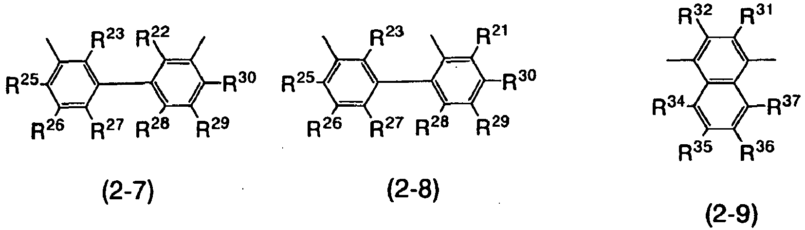

- In addition, in the above structure, Ar1 and Ar 2 in the general formula (1) are represented by any of the following general formulas (3-1) to (3-6).


- Further, in the above structure, R 1 in the general formula (1) is represented by any of the following general formulas (4-1) to (4-9), and R 2 in the general formula (1) is represented by any of the following general formulas (4-2) to (4-9).


- In addition, one feature of the present invention is represented by any of the following structural formulas (5) to (8).


- In addition, as another feature of the present invention, a light-emitting element includes an EL layer between a pair of electrodes, the EL layer includes at least a light-emitting layer and a hole-transporting layer, and at least one of the light-emitting layer and the hole-transporting layer contains any of the carbazole derivatives described above.
- Further, as another feature of the present invention, a light-emitting element includes an EL layer between an anode and a cathode, the EL layer includes at least a light-emitting layer, a hole-transporting layer, and a hole-injecting layer, the hole-injecting layer is formed in contact with the anode, and at least one of the light-emitting layer, the hole-transporting layer, and the hole-injecting layer contains any of the carbazole derivatives described above.
- In addition, in the above structure, a structure may be employed in which the hole-injecting layer contains any of the carbazole derivatives described above and an inorganic compound which exhibits an electron-accepting property with respect to the carbazole derivative. Note that as the inorganic compound, an oxide of a transition metal can be used. Further, as the inorganic compound, one or more kinds of titanium oxide, vanadium oxide, molybdenum oxide, tungsten oxide, rhenium oxide, ruthenium oxide, chromium oxide, zirconium oxide, hafnium oxide, tantalum oxide, and silver oxide can be used.
- Further, as another feature of the present invention, a light-emitting device is formed using any of the light-emitting elements described above, and an electronic device is formed using the light-emitting device.
- Further, the present invention also includes a light-emitting device having the light-emitting element described above and an electronic devuce having the light-emitting device. A light-emitting device in this specification refers to an image display device, a light-emitting device, or a light source (including a lighting device). In addition, light-emitting devices include all of the following modules: modules in which a connector, for example, a flexible printed circuit (FPC), a tape automated bonding (TAB) tape, or a tape carrier package (TCP) is attached to a light-emitting device; modules provided with a printed wiring board at the end of a TAB tape or a TCP; and modules where an integrated circuit (IC) is directly mounted on a light-emitting element by a chip-on-glass (COG) method.
- Since the carbazole derivative of the present invention exhibits a high hole-transporting property, it can be mainly used for a hole-transporting layer which is included in an EL layer of a light-emitting element. In addition, the carbazole derivative of the present invention is used for the hole-transporting layer to form a light-emitting element, whereby a light-emitting element having high luminous efficiency can be formed.
- Further, a light-emitting device and an electronic device which consumes low power and is driven at low voltage can be obtained by using this light-emitting element.
- In the accompanying drawings:
-
FIGS. 1A and 1B are cross-sectional views each showing a stacked-layer structure of a light-emitting element inEmbodiment Mode 2; -
FIGS. 2A to 2C are cross-sectional views each showing a mode of light emission of a light-emitting element inEmbodiment Mode 2; -
FIG 3 is a cross-sectional view showing a stacked-layer structure of a light-emitting element inEmbodiment Mode 3; -
FIGS. 4A and 4B are respectively a top view and a cross-sectional view of an active matrix light-emitting device inEmbodiment Mode 4; -
FIGS. 5A and 5B are respectively a perspective view and a cross-sectional view of a passive matrix light-emitting device inEmbodiment Mode 4; -
FIGS. 6A to 6D are views each showing an electronic device inEmbodiment Mode 5; -
FIG. 7 is a view showing a liquid crystal display device using a light-emitting device of the present invention as a backlight; -
FIG. 8 is a view showing a table lamp using a light-emitting device of the present invention; -
FIG 9 is a view showing an indoor lighting device using a light-emitting device of the present invention; -
FIGS. 10A and 10B are graphs showing 1H NMR charts of PCBA1BP (abbreviation); -
FIGS. 11A and 11B are graphs showing an absorption spectrum and an emission spectrum of PCBA1BP (abbreviation); -
FIGS. 12A and 12B are graphs showing 1H NMR charts of PCBBi1BP (abbreviation); -
FIGS. 13A and 13B are graphs showing an absorption spectrum and an emission spectrum of PCBBi1BP (abbreviation); -
FIGS. 14A and 14B are graphs showing 1H NMR charts of PCBAF (abbreviation); -
FIGS. 15A and 15B are graphs showing an absorption spectrum and an emission spectrum of PCBAF (abbreviation); -
FIGS. 16A and 16B are graphs showing 1H NMR charts of PCBASF (abbreviation); -
FIGS. 17A and 17B are graphs showing an absorption spectrum and an emission spectrum of PCBASF (abbreviation); -
FIG. 18 is a cross-sectional view showing an element structure of a light-emitting element inEmbodiment 5; -
FIG 19 is a graph showing the current density vs. luminance characteristics of a light-emittingelement 1 and a light-emittingelement 2; -
FIG 20 is a graph showing the voltage vs. luminance characteristics of the light-emittingelement 1 and the light-emittingelement 2; -
FIG 21 is a graph showing the luminance vs. current efficiency characteristics of the light-emittingelement 1 and the light-emittingelement 2; -
FIG 22 is a graph showing the voltage vs. current characteristics of the light-emittingelement 1 and the light-emittingelement 2; -
FIG. 23 is a graph showing emission spectra of the light-emittingelement 1 and the light-emittingelement 2; -
FIG. 24 is a graph showing the result of a continuous lighting test of the light-emittingelement 1 and the light-emittingelement 2 by constant current driving; -
FIG. 25 is a graph showing the current density vs. luminance characteristics of the light-emittingelement 1 and a light-emittingelement 3; -
FIG. 26 is a graph showing the voltage vs. luminance characteristics of the light-emittingelement 1 and the light-emittingelement 3; -
FIG. 27 is a graph showing the luminance vs. current efficiency characteristics of the light-emittingelement 1 and the light-emittingelement 3; -
FIG. 28 is a graph showing the voltage vs. current characteristics of the light-emittingelement 1 and the light-emittingelement 3; -
FIG. 29 is a graph showing emission spectra of the light-emittingelement 1 and the light-emittingelement 3; -
FIG. 30 is a graph showing the current density vs. luminance characteristics of the light-emittingelement 1 and a light-emittingelement 4; -
FIG. 31 is a graph showing the voltage vs. luminance characteristics of the light-emittingelement 1 and the light-emittingelement 4; -
FIG. 32 is a graph showing the luminance vs. current efficinecy characteristics of the light-emittingelement 1 and the light-emittingelement 4; -
FIG. 33 is a graph showing the voltage vs. current characteristics of the light-emittingelement 1 and the light-emittingelement 4; -
FIG. 34 is a graph showing emission spectra of the light-emittingelement 1 and the light-emittingelement 4; -
FIG. 35 is a graph showing the result of a continuous lighting test of the light-emittingelement 1 and the light-emittingelement 4 by constant current driving; -
FIG 36 is a graph showing the current density vs. luminance characteristics of the light-emittingelement 1 and a light-emittingelement 5; -
FIG. 37 is a graph showing the voltage vs. luminance characteristics of the light-emittingelement 1 and the light-emittingelement 5; -
FIG. 38 is a graph showing the luminance vs. current efficinecy characteristics of the light-emittingelement 1 and the light-emittingelement 5; -
FIG. 39 is a graph showing the voltage vs. current characteristics of the light-emittingelement 1 and the light-emittingelement 5; -
FIG. 40 is a graph showing emission spectra of the light-emittingelement 1 and the light-emittingelement 5; -
FIG. 41 is a graph showing CV characteristics of PCBA1BP (abbreviation); -
FIG. 42 is a graph showing CV characteristics of PCBBi1BP (abbreviation); -
FIG 43 is a graph showing CV characteristics of PCBAF (abbreviation); -
FIG. 44 is a graph showing CV characteristics of PCBASF (abbreviation); -
FIGS. 45A and 45B are graphs showing 1H NMR charts of PCTA1BP (abbreviation); -
FIGS. 46A and 46B are graphs showing 1H NMR charts of PCTBi1BP (abbreviation); -
FIGS. 47A and 47B are graphs showing 1H NMR charts of PCBANB (abbreviation); -
FIGS. 48A and 48B are graphs showing 1H NMR charts of PCBNBB (abbreviation); -
FIGS. 49A and 49B are graphs showing 1H NMR charts of PCBBiNB (abbreviation); -
FIGS. 50A and 50B are graphs showing 1H NMR charts of PCBANT (abbreviation); -
FIGS. 51A and 51B are graphs showing 1H NMR charts of BCBA1BP (abbreviation); -
FIGS. 52A and 52B are graphs showing 1H NMR charts of BCBANB (abbreviation); -
FIGS. 53A and 53B are graphs showing 1H NMR charts of BCBBiNB (abbreviation); -
FIGS. 54A and 54B are graphs showing 1H NMR charts of NBCBA1BP (abbreviation); -
FIGS. 55A and 55B are graphs showing 1H NMR charts of NCBA1BP (abbreviation); -
FIG 56 is a graph showing the voltage vs. luminance characteristics of the light-emittingelement 1 and light-emittingelements 6 to 8; -
FIG. 57 is a graph showing the luminance vs. current efficinecy characteristics of the light-emittingelement 1 and the light-emittingelements 6 to 8; -
FIG. 58 is a graph showing the voltage vs. current characteristics of the light-emittingelement 1 and the light-emittingelements 6 to 8; -
FIG. 59 is a graph showing emission spectra of the light-emittingelement 1 and the light-emittingelements 6 to 8; -
FIG. 60 is a graph showing the result of a continuous lighting test of the light-emittingelement 1 and the light-emittingelements 6 to 8 by constant current driving; -
FIGS. 61A and 61B are graphs showing 1H NMR charts of PCBBi1BPIII (abbreviation); -
FIGS. 62A to 62C are graphs showing 1H NMR charts of PCBA1BPIV (abbreviation); -
FIGS. 63A and 63B are graphs showing 1H NMR charts of PCBNBBβ (abbreviation); and -
FIGS. 64A and 64B are graphs showing 1H NMR charts of PCBBiFLP (abbreviation). - The embodiment modes and embodiments according to the present invention will hereinafter be described in detail with reference to the drawings. However, the present invention is not limited to description to be given below, and it is to be easily understood that modes and details thereof can be variously modified without departing from the purpose and the scope of the present invention. Thus, the present invention is not interpreted while limiting to the following description of the embodiment modes and embodiments.
- In
Embodiment Mode 1, a carbazole derivative of the present invention will be described. - The carbazole derivative of the present invention is represented by a general formula (1).

- In the formula, α 1, α 2, α 3, and α 4 each represent an arylene group having less than or equal to 13 carbon atoms, which forms a ring; Ar 1 and Ar 2 each represent an aryl group having less than or equal to 13 carbon atoms, which forms a ring; R 1 represents any of a hydrogen atom, an alkyl group having 1 to 6 carbon atoms, a substituted or unsubstituted phenyl group, and a substituted or unsubstituted biphenyl group; and R 2 represents any of alkyl group having 1 to 6 carbon atoms, a substituted or unsubstituted phenyl group, and a substituted or unsubstituted biphenyl group. In addition, l, m, and n are each independent, which is 0 or 1.
- In the general formula (1), α 1 to α 4 each represent an arylene group having less than or equal to 13 carbon atoms, which forms a ring. Specifically, substituents represented by structural formulas (2-1) to (2-12) can be given.


- In the formula, R 11 to R 16, R 21 to R 30, R 31 to R 38, and R 41 to R 45 each represent any of a hydrogen atom, an alkyl group having 1 to 6 carbon atoms, a phenyl group, and a biphenyl group. R 46 and R 47 each represent any of an alkyl group having 1 to 6 carbon atoms and a phenyl group. In addition, R 46 and R 47 may be connected to each other to form a ring. R 48 represents any of a hydrogen atom, an alkyl group having 1 to 6 carbon atoms, a phenyl group, and a biphenyl group.
- In the general formula (1),Ar 1 and Ar 2 each represent an aryl group having less than or equal to 13 carbon atoms, which forms a ring. Specifically, substituents represented by structural formulas (3-1) to (3-6) can be given.


- In the formula, R 51 to R 56, R 61 to R 70, R 71 to R 78, and R 81 to R 85 each represent any of a hydrogen atom, an alkyl group having 1 to 6 carbon atoms, a phenyl group, and a biphenyl group. R 86 and R 87 each represent any of an alkyl group having 1 to 6 carbon atoms and a phenyl group. In addition, R 86 and R 87 may be connected to each other to form a ring. R 88 and R 89 each represent any of a hydrogen atom, an alkyl group having 1 to 6 carbon atoms, a phenyl group, and a biphenyl group.
- In the general formula (1), R 1 represents any of a hydrogen atom, an alkyl group having 1 to 6 carbon atoms, a substituted or unsubstituted phenyl group, and a substituted or unsubstituted biphenyl group; and R 2 represents any of an alkyl group having 1 to 6 carbon atoms, a substituted or unsubstituted phenyl group, and a substituted or unsubstituted biphenyl group. Specifically, substituents represented by structural formulas (4-1) to (4-9) can be given for R 1, and the substituents represented by the structural formulas (4-2) to (4-9) can be given for R 2.


- In the formula, R 51 to R 70 each represent any of a hydrogen atom, an alkyl group having 1 to 6 carbon atoms, a phenyl group, and a biphenyl group.
- As a specific example of the carbazole derivatives of the present invention represented by the general formula (1), carbazole derivatives represented by structural formulas (9) to (425) can be given. However, the present invention is not limited thereto.


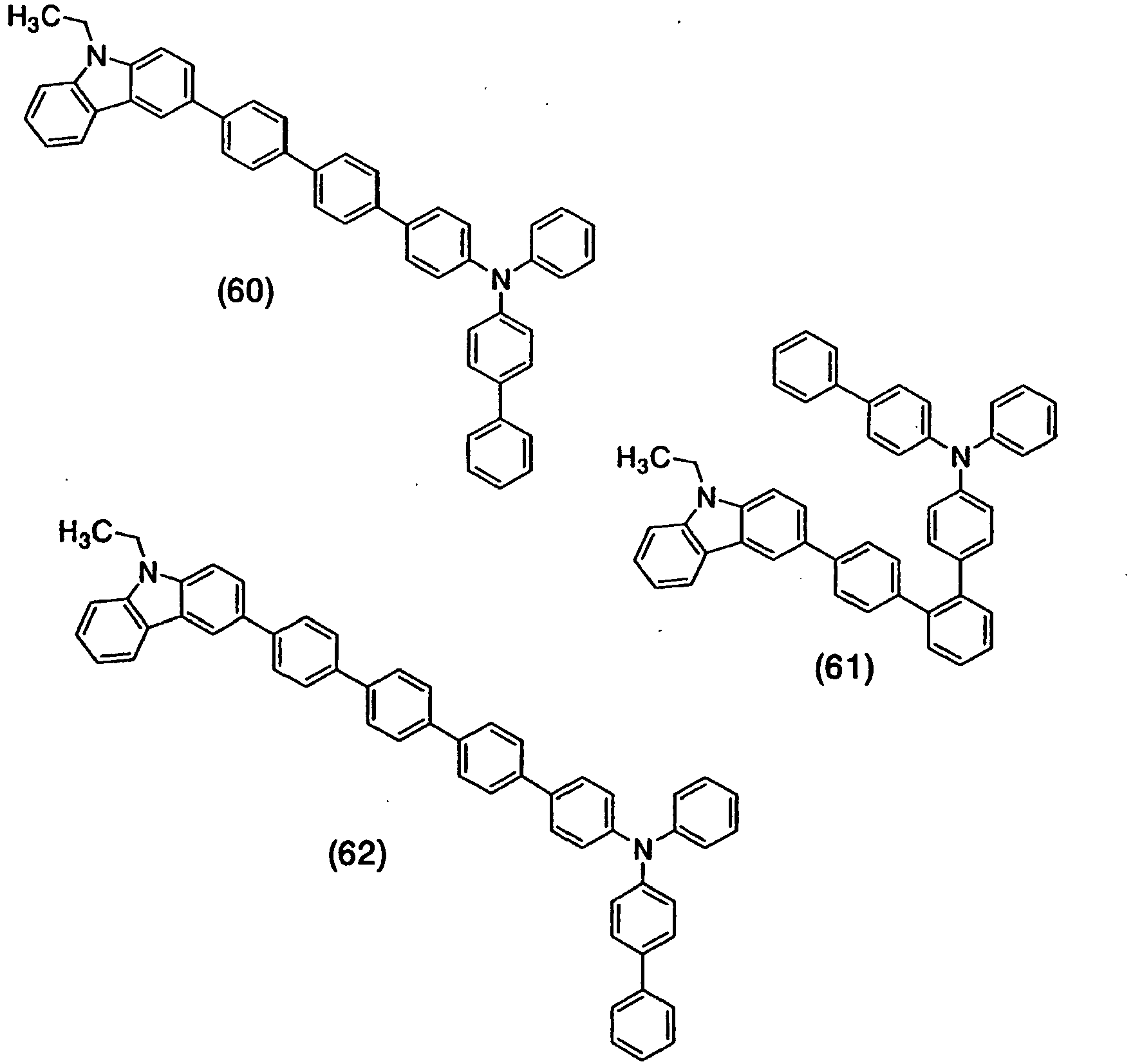


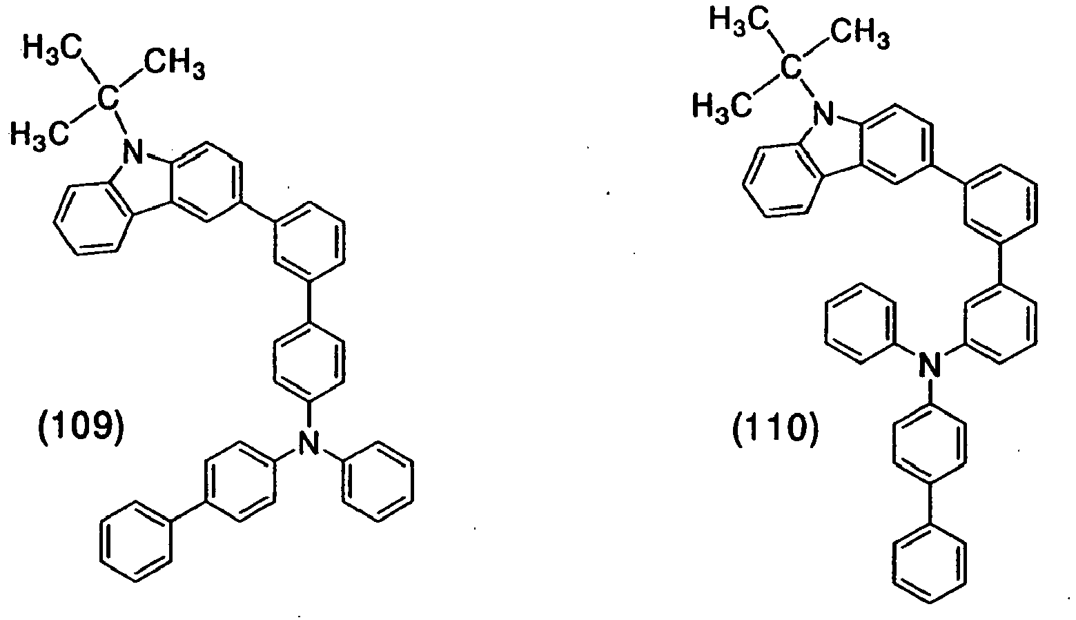


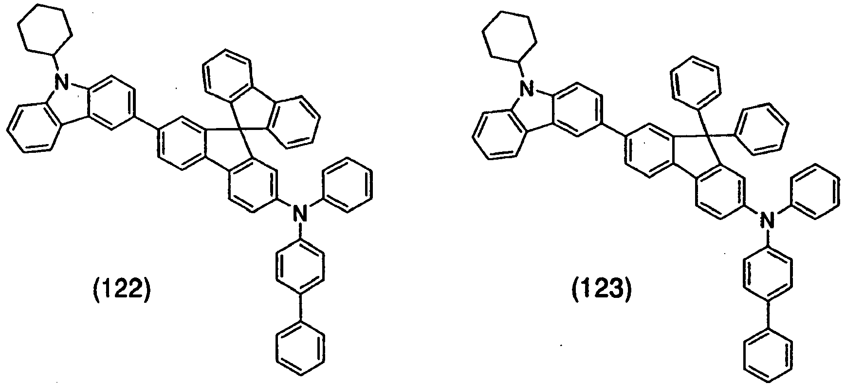


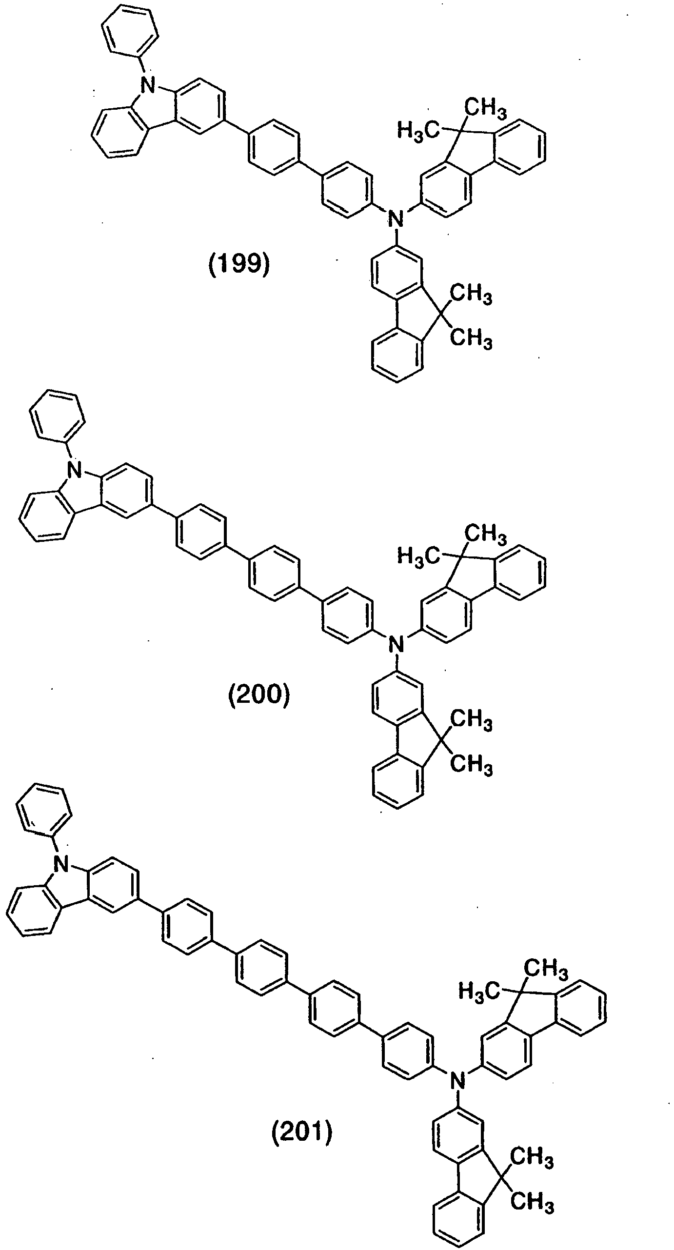


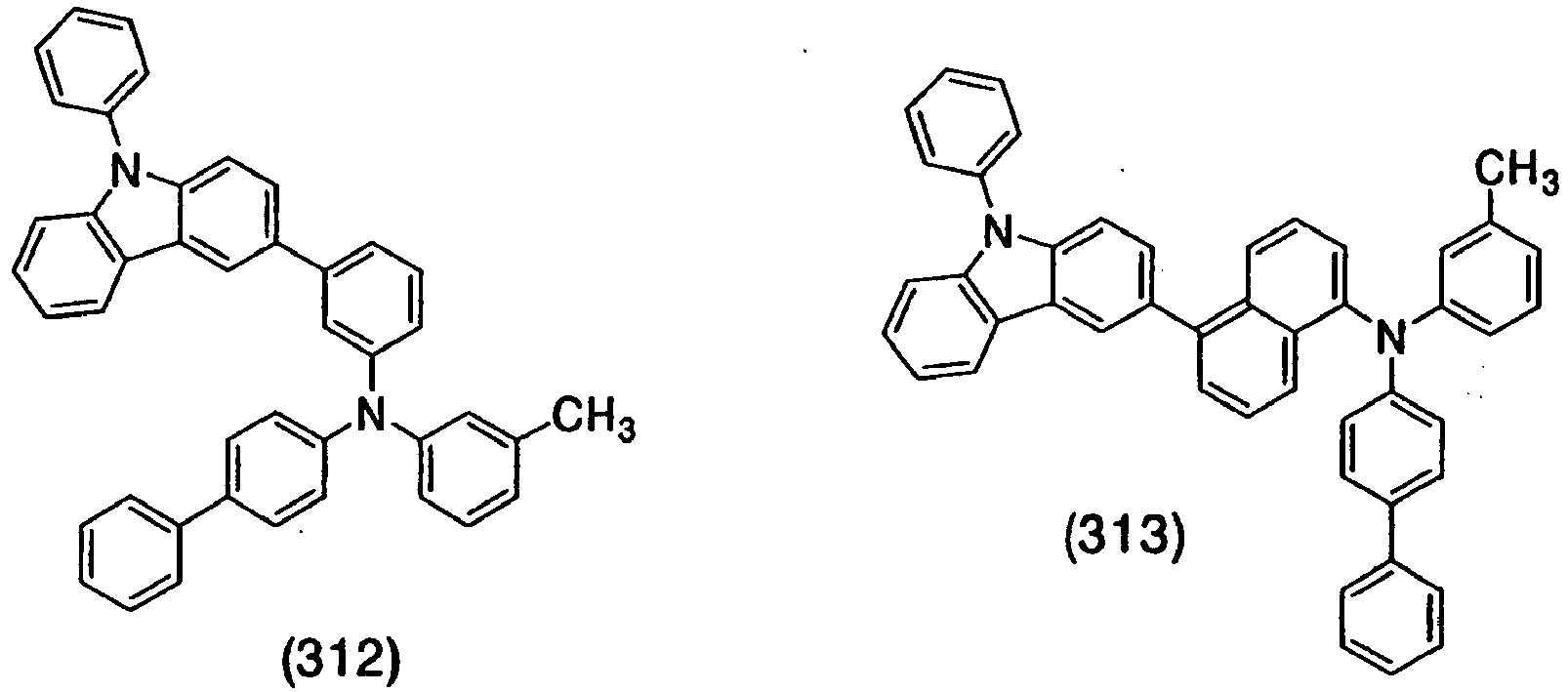


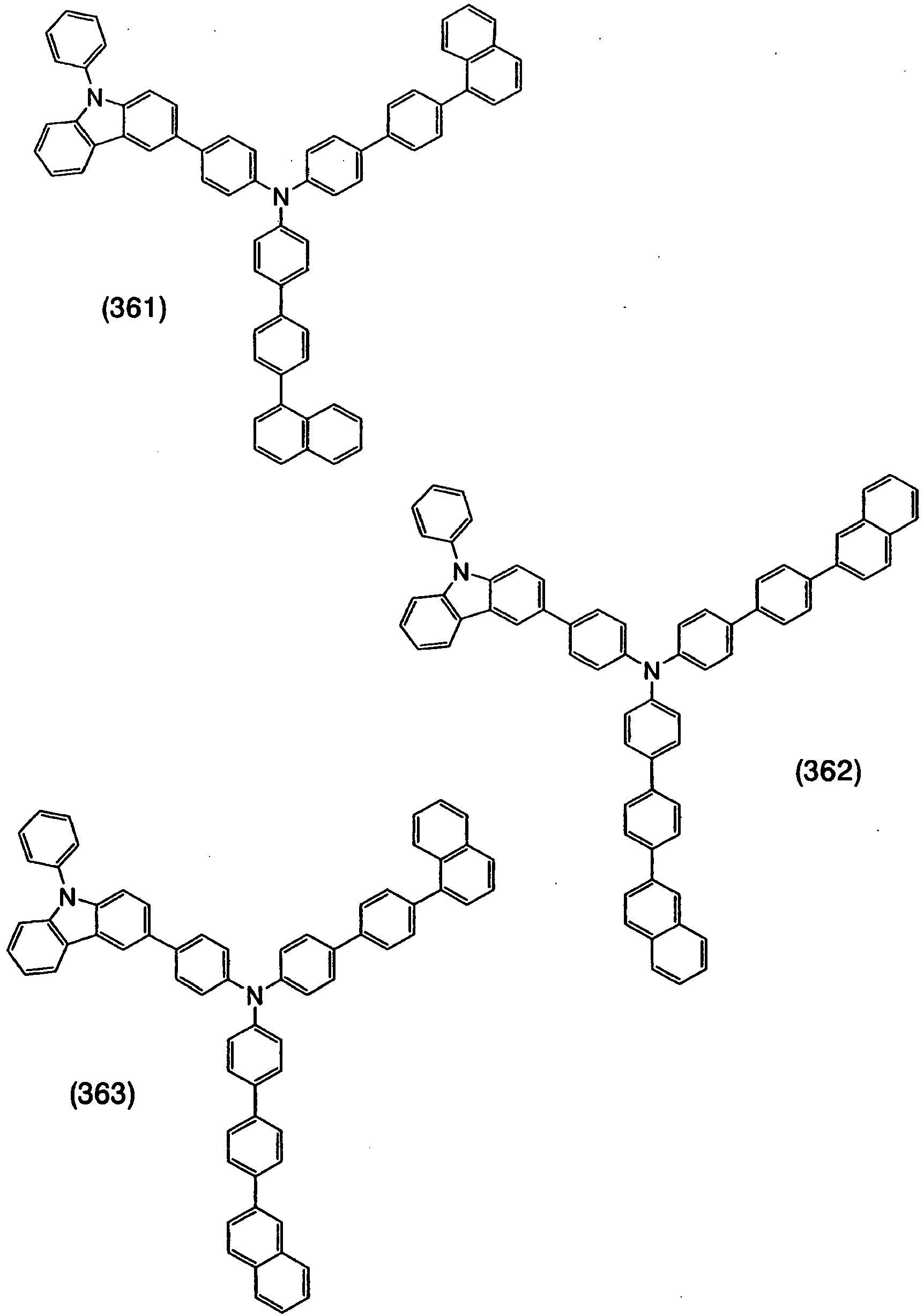


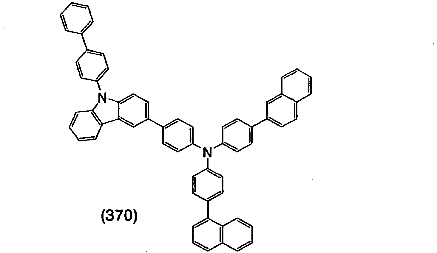


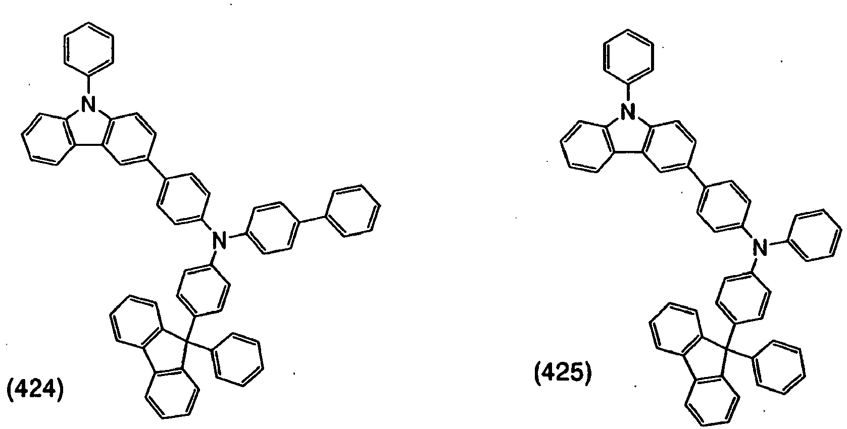
- In addition, the carbazole derivative of the present invention represented by the general formula (1) can be synthesized by a synthetic method represented by the following synthetic schemes (A-1) to (A-7), a synthetic scheme (B-1), and synthetic schemes (C-1) to (C-2).
- Halogenated secondary arylamine represented by a general formula (compound A) can be synthesized in a manner like the following synthetic scheme (A-1). In other words, first, secondary arylamine (compound A1) is halogenated by using a halogenating agent, whereby the halogenated secondary arylamine (compound A) can be obtained. Note that as the halogenating agent, N-bromosuccinimide (NBS), N-iodosuccinimide (NIS), bromine, iodine, potassium iodide, or the like can be used. In addition, each X1 represents a halogen group, which is preferably a bromo group or an iodine group.

- A halogenated carbazole derivative represented by a general formula (compound B2) can be synthesized in a manner like the following synthetic scheme (A-2). In other words, first, a carbazole derivative (compound B1) is halogenated by using a halogenating agent, whereby the halogenated carbazole derivative (compound B2) can be obtained. Note that as the halogenating agent, N-bromosuccinimide (NBS), N-iodosuccinimide (NIS), bromine, iodine, potassium iodide, or the like can be used. In addition, each X1 represents a halogen group, which is preferably a bromo group or an iodine group.

- A compound in which the third position of 9H-carbazole is substituted by boronic acid or organoboron, which is represented by a general formula (compound B), can be synthesized in a manner like the following synthetic scheme (A-3). In other words, boron oxidation or organoboronation is performed on the halogenated carbazole derivative (compound B2) using an alkyllithium reagent and a boron reagent, whereby the compound in which the third position of 9H-carbazole is substituted by boronic acid or organoboron (compound B) can be obtained.
- Note that R 99 in the scheme (A-3) represents an alkyl group having 1 to 6 carbon atoms. R 98 presents an alkyl group having 1 to 6 carbon atoms. In addition, R 100 and R 101 each represent a hydrogen atom or an alkyl group having 1 to 6 carbon atoms. R 102 and R 103 may be connected to each other to form a ring. In addition, n-butyllithium, methyllithium, or the like can be used as the alkyllithium reagent. Trimethyl borate, isopropyl borate, or the like can be used as the boron reagent.

- Secondary arylamine represented by a general formula (compound C3) can be synthesized in a manner like the following synthetic scheme (A-4). In other words, halogenated aryl (compound C1) and primary arylamine (compound C2) are coupled in the presence of a base using a metal catalyst, whereby the secondary arylamine (compound C3) can be obtained.

- In the case where a Buchwald-Hartwig reaction is performed, as the palladium catalyst which can be used in the synthetic scheme (A-4), although bis(dibenzylideneacetone)palladium(0), palladium(II) acetate, and the like can be given, the palladium catalyst which can be used is not limited thereto. As a ligand in the palladium catalyst which can be used in the synthetic scheme (A-4), although tri(tert-butyl)phosphine, tri(n-hexyl)phosphine, tricyclohexylphosphine, and the like can be given, the ligand which can be used is not limited thereto.
- As a base which can be used in the synthetic scheme (A-4), although an organic base such as sodium tert-butoxide, an inorganic base such as potassium carbonate, and the like can be given, the base which can be used is not limited thereto. In addition, as a solvent that can be used in the synthetic scheme (A-4), although toluene, xylene, benzene, tetrahydrofuran, and the like can be given, the solvent which can be used is not limited thereto.
- The case in which an Ullmann reaction is performed in the synthetic scheme (A-4) is described. In the synthetic scheme (A-4), R 104 and R 105 each represent a halogen group, an acetyl group, or the like, and chlorine, bromine, and iodine can be given as the halogen group. It is preferable that R 104 be iodine to form copper(I) iodide or that R 105 be an acetyl group to form a copper(II) acetate. The copper compound used for the reaction is not limited thereto, and copper can be used as an alternative to the copper compound. As a base which can be used in the synthetic scheme (A-4), although an inorganic base such as potassium carbonate can be given, the base which can be used is not limited thereto.
- As a solvent which can be used in the synthetic scheme (A-4), although 1,3-dimethyl-3,4,5,6-tetrahydro-2(1H)pyrimidinone (abbreviation: DMPU), toluene, xylene, benzene, and the like can be given, the solvent which can be used is not limited thereto. DMPU or xylene which has a high boiling point is preferably used because, by an Ullmann reaction, an object can be obtained in a shorter time and at a higher yield when the reaction temperature is greater than or equal to 100 °C. Since it is further preferable that the reaction temperature be a temperature greater than or equal to 150 °C, DMPU is more preferably used.
- Tertiary arylamine represented by a general formula (compound C5) can be synthesized in a manner like the following synthetic scheme (A-5). In other words, the secondary arylamine (compound C3) and halogenated aryl (compound C4) are coupled in the presence of a base using a metal catalyst, whereby the tertiary arylamine (compound C5) can be obtained.

- In the case where a Buchwald-Hartwig reaction is performed, as the palladium catalyst which can be used in the synthetic scheme (A-5), although bis(dibenzylideneacetone)palladium(0), palladium(II) acetate, and the like can be given, the palladium catalyst which can be used is not limited thereto. As a ligand in the palladium catalyst which can be used in the synthetic scheme (A-5), although tri(tert-butyl)phosphine, tri(n-hexyl)phosphine, tricyclohexylphosphine, and the like can be given, the ligand which can be used is not limited thereto.
- As a base which can be used in the synthetic scheme (A-5), although an organic base such as sodium tert-butoxide, an inorganic base such as potassium carbonate, and the like can be given, the base which can be used is not limited thereto. In addition, as a solvent that can be used in the synthetic scheme (A-5), although toluene, xylene, benzene, tetrahydrofuran, and the like can be given, the solvent which can be used is not limited thereto.
- The case in which an Ullmann reaction is performed in the synthetic scheme (A-5) is described. In the synthetic scheme (A-5), R 104 and R 105 each represent a halogen group, an acetyl group, or the like, and chlorine, bromine, and iodine can be given as the halogen group. It is preferable that R 104 be iodine to form copper(I) iodide or that R 105 be an acetyl group to form a copper(II) acetate. The copper compound used for the reaction is not limited thereto, and copper can be used as an alternative to the copper compound. As a base which can be used in the synthetic scheme (A-5), although an inorganic base such as potassium carbonate can be given, the base which can be used is not limited thereto.
- As a solvent which can be used in the synthetic scheme (A-5), although 1,3-dimethyl-3,4,5,6-tetrahydro-2(1H)pyrimidinone (abbreviation: DMPU), toluene, xylene, benzene, and the like can be given, the solvent which can be used is not limited thereto. DMPU or xylene which has a high boiling point is preferably used because, by an Ullmann reaction, an object can be obtained in a shorter time and at a higher yield when the reaction temperature is greater than or equal to 100 °C. Since it is further preferable that the reaction temperature be a temperature greater than or equal to 150 °C, DMPU is more preferably used.
- Tertiary arylamine represented by a general formula (compound C5) can be synthesized in a manner like the following synthetic scheme (A-6). In other words, the primary arylamine (compound C2) and the halogenated aryl (compounds C1 and C4) are coupled in the presence of a base using a metal catalyst, whereby the tertiary arylamine (compound C5) can be obtained. However, when Ar 1 and Ar 2 are the same, β 1 and β 2 are the same, and l and m are the same, the compound C5 can be obtained with high yield.

- In the case where a Buchwald-Hartwig reaction is performed, as the palladium catalyst which can be used in the synthetic scheme (A-6), although bis(dibenzylideneacetone)palladium(0), palladium(II) acetate, and the like can be given, the palladium catalyst which can be used is not limited thereto. As a ligand in the palladium catalyst which can be used in the synthetic scheme (A-6), although tri(tert-butyl)phosphine, tri(n-hexyl)phosphine, tricyclohexylphosphine, and the like can be given, the ligand which can be used is not limited thereto.
- As a base which can be used in the synthetic scheme (A-6), although an organic base such as sodium tert-butoxide, an inorganic base such as potassium carbonate, and the like can be given, the base which can be used is not limited thereto. In addition, as a solvent that can be used in the synthetic scheme (A-6), although toluene, xylene, benzene, tetrahydrofuran, and the like can be given, the solvent which can be used is not limited thereto.
- The case in which an Ullmann reaction is performed in the synthetic scheme (A-6) is described. In the synthetic scheme (A-6), R 104 and R 105 each represent a halogen group, an acetyl group, or the like, and chlorine, bromine, and iodine can be given as the halogen group. It is preferable that R 104 be iodine to form copper(I) iodide or that R 105 be an acetyl group to form a copper(II) acetate. The copper compound used for the reaction is not limited thereto, and copper can be used as an alternative to the copper compound. As a base which can be used in the synthetic scheme (A-6), although an inorganic base such as potassium carbonate can be given, the base which can be used is not limited thereto.
- As a solvent which can be used in the synthetic scheme (A-6), although 1,3-dimethyl-3,4,5,6-tetrahydro-2(1H)pyrimidinone (abbreviation: DMPU), toluene, xylene, benzene, and the like can be given, the solvent which can be used is not limited thereto. DMPU or xylene which has a high boiling point is preferably used because, by an Ullmann reaction, an object can be obtained in a shorter time and at a higher yield when the reaction temperature is greater than or equal to 100 °C. Since it is further preferable that the reaction temperature be a temperature greater than or equal to 150 °C, DMPU is more preferably used.
- Halogenated tertiary arylamine represented by a general formula (compound C) can be synthesized in a manner like the following synthetic scheme (A-7). In other words, first, tertiary arylamine (compound C5) is halogenated by using a halogenating agent, whereby the halogenated tertiary arylamine (compound C) can be obtained. Note that as the halogenating agent, N-bromosuccinimide (NBS), N-iodosuccinimide (NIS), bromine, iodine, potassium iodide, or the like can be used. In addition, each X1 represents a halogen group, which is preferably a bromo group or an iodine group.

- Secondary arylamine having carbazole, which is represented by a general formula (compound D), can be synthesized in a manner like the following synthetic scheme (B-1). In other words, the halogenated secondary arylamine (compound A) and the compound in which the third position of 9H-carbazole is substituted by boronic acid or organoboron (compound B) can be coupled in the presence of a base using a metal catalyst. Accordingly, the secondary arylamine having carbazole (compound D) can be obtained.

- In any of the above schemes, the case of using a Suzuki-Miyaura reaction is described. As a palladium catalyst which can be used as a metal catalyst, palladium(II) acetate, tetrakis(triphenylphosphine)palladium(0), bis(triphenylphosphine)palladium(II)dichloride, and the like can be given. As a ligand in the above palladium catalyst, tri(ortho-tolyl)phosphine, triphenylphosphine, tricyclohexylphosphine, and the like can be given. In addition, as the above base, an organic base such as sodium tert-butoxide, an inorganic base such as potassium carbonate, and the like can be given. As the solvent which can be used, a mixed solvent of toluene and water; a mixed solvent of toluene, an alcohol such as ethanol, and water; a mixed solvent of xylene and water; a mixed solvent of xylene, an alcohol such as ethanol, and water; a mixed solvent of benzene and water; a mixed solvent of benzene, an alcohol such as ethanol, and water; a mixed solvent of ethers such as ethyleneglycoldimethylether and water; and the like can be given.
- However, the catalyst, ligand, base, and solvent which can be used are not limited thereto.
- In addition, in any of the above schemes, cross coupling using organoaluminum, organozirconium, organozinc, or organotin compound, or the like, in addition to arylboronic acid, may be employed as a base material. However, the present invention is not limited thereto.
- Tertiary arylamine having carbazole represented by a general formula (compound E) can be synthesized in a manner like the following synthetic scheme (C-1). In other words, the secondary arylamine having carbazole (compound D) and the halogenated aryl (compound C4) are coupled in the presence of a base using a metal catalyst, whereby the tertiary arylamine having carbazole (compound E), which is a final product, can be obtained.

- In any of the above schemes, the case of using a Suzuki-Miyaura reaction is described. As a palladium catalyst which can be used as a metal catalyst, palladium(II) acetate, tetrakis(triphenylphosphine)palladium(0), bis(triphenylphosphine)palladium(II)dichloride, and the like can be given. As a ligand in the above palladium catalyst, tri(ortho-tolyl)phosphine, triphenylphosphine, tricyclohexylphosphine, and the like can be given. In addition, as the above base, an organic base such as sodium tert-butoxide, an inorganic base such as potassium carbonate, and the like can be given. As the solvent which can be used, a mixed solvent of toluene and water; a mixed solvent of toluene, an alcohol such as ethanol, and water; a mixed solvent of xylene and water; a mixed solvent of xylene, an alcohol such as ethanol, and water; a mixed solvent of benzene and water; a mixed solvent of benzene, an alcohol such as ethanol, and water; a mixed solvent of ethers such as ethyleneglycoldimethylether and water; and the like can be given.
- However, the catalyst, ligand, base, and solvent which can be used are not limited thereto.
- In addition, in any of the above schemes, cross coupling using organoaluminum, organic zirconium, organozinc, organozirconium, organotin, or the like, in addition to arylboronic acid, may be employed as a base material. However, the present invention is not limited thereto.
- The tertiary arylamine having carbazole represented by the general formula (compound E) can be synthesized in a manner like the following synthetic scheme (C-2). In other words, first, the halogenated tertiary arylamine (compound C) and the compound in which the third position of 9H-carbazole is substituted by boronic acid or organoboron (compound B) are coupled in the presence of a base using a metal catalyst, whereby the tertiary arylamine having carbazole (compound E), which is a final product, can be obtained.

- In
Embodiment Mode 2, a light-emitting element which is formed using, for a hole-transporting layer, the carbazole derivative of the present invention described inEmbodiment Mode 1 will be described. - The light-emitting element in
Embodiment Mode 2 includes a first electrode which functions as an anode, a second electrode which functions as a cathode, and an EL layer interposed between the first electrode and the second electrode. Note that the light-emitting element inEmbodiment Mode 2 can obtain light emission when voltage is applied to each electrode so that the potential of the first electrode is higher than that of the second electrode. - In addition, the EL layer of the light-emitting element in
Embodiment Mode 2 includes in its structure a first layer (a hole-injecting layer), a second layer (a hole-transporting layer), a third layer (a light-emitting layer), a fourth layer (an electron-transporting layer), and a fifth layer (an electron-injecting layer), from the first electrode side. - A structure of the light-emitting element in
Embodiment Mode 2 is described with reference toFIGS. 1A and 1B . Asubstrate 101 is used as a support of the light-emitting element. For thesubstrate 101, glass, quartz, plastics, or the like can be used, for example. - Note that although the
above substrate 101 may remain in a light-emitting device or an electronic device which is a product utilizing the light-emitting element of the present invention, thesubstrate 101 may only have a function as the support of the light-emitting element in the manufacturing process of the light-emitting element, without remaining in an end product. - For a
first electrode 102 formed over thesubstrate 101, a metal, an alloy, an electrically conductive compound, a mixture thereof, or the like having a high work function (specifically, a work function of 4.0 eV or more) is preferably used. Specifically, the following examples can be given: indium tin oxide (ITO), indium tin oxide containing silicon or silicon oxide, indium zinc oxide (IZO), and indium oxide containing tungsten oxide and zinc oxide. Besides, gold (Au), platinum (Pt), nickel (Ni), tungsten (W), chromium (Cr), molybdenum (Mo), iron (Fe), cobalt (Co), copper (Cu), palladium (Pd), titanium (Ti), nitrides of the metal materials (e.g., titanium nitride), and the like can be given. However, in the present invention, afirst layer 111 in anEL layer 103 which is formed in contact with thefirst electrode 102 is formed using a composite material with which holes are easily injected regardless of the work function of thefirst electrode 102. Therefore, a variety of known methods can be used as long as it is a material that can serve as an electrode material (e.g., a metal, an alloy, an electrically conductive compound, a mixture thereof, or the like, or an element belonging toGroup - A film of any of those materials is generally formed by a sputtering method. For example, indium zinc oxide (IZO) can be formed by a sputtering method using a target in which 1 wt% to 20 wt% zinc oxide is added to indium oxide; and indium oxide containing tungsten oxide and zinc oxide can be formed by a sputtering method using a target in which 0.5 wt% to 5 wt% tungsten oxide and 0.1 wt% to 1 wt% zinc oxide are added to indium oxide. Alternatively, the
first layer 111 may be formed by a vacuum evaporation method, an ink-jet method, a spin-coating method, or the like. - Further, when a layer containing a composite material which will be described later is used as a material used for the
first layer 111 formed in contact with thefirst electrode 102 in theEL layer 103 formed over thefirst electrode 102, any of a variety of materials such as metals, alloys, and electrically conductive compounds; a mixture thereof; or the like can be used as a substance used for thefirst electrode 102 regardless of their work functions. For example, aluminum (Al), silver (Ag), an alloy containing aluminum (AlSi), or the like can also be used. - Furthermore, an element belonging to
Group - Note that in the case where the
first electrode 102 is formed using an alkali metal, an alkaline-earth metal, or an alloy thereof, a vacuum evaporation method or a sputtering method can be employed. Note that in the case of using a silver paste or the like, a coating method, an ink-jet method, or the like can be used. - For the
EL layer 103 formed over thefirst electrode 102, a known substance can be used, and any of a low molecular compound and a macromolecular compound can be used. Note that the substance used to form theEL layer 103 has not only a structure formed of only an organic compound but also a structure partially containing an inorganic compound. - For forming the
EL layer 103, a hole-injecting layer containing a substance having a high hole-injecting property, a hole-transporting layer containing a substance having a high hole-transporting property, a light-emitting layer containing a light-emitting substance, an electron-transporting layer containing a substance having a high electron-transporting property, an electron-injecting layer containing a substance having a high electron-injecting property, and the like are combined with each other and stacked, as appropriate. - Note that in the
EL layer 103 shown inFIG 1A , the first layer (a hole-injecting layer) 111, a second layer (a hole-transporting layer) 112, a third layer (a light-emitting layer) 113, a fourth layer (an electron-transporting layer) 114, and a fifth layer (an electron-injecting layer) 115 are sequentially stacked from thefirst electrode 102 side. - The
first layer 111 which is a hole-injecting layer is a hole-injecting layer containing a substance having a high hole-injecting property. As the substance having a high hole-injecting property, molybdenum oxide, titanium oxide, vanadium oxide, rhenium oxide, ruthenium oxide, chromium oxide, zirconium oxide, hafnium oxide, tantalum oxide, silver oxide, tungsten oxide, manganese oxide, or the like can be used. Alternatively, as a low-molecular organic compound, a phthalocyanine-based compound such as phthalocyanine (abbreviation: H2Pc), copper(II) phthalocyanine (abbreviation: CuPc), or vanadyl phthalocyanine (abbreviation: VOPc) can be given. - In addition, the following aromatic amine compounds which are low-molecular organic compounds can also be given: 4,4',4"-tris(N,N-diphenylamino)triphenylamine (abbreviation: TDATA); 4,4',4"-tris[N-(3-methylphenyl)-N-phenylamino]triphenylamine (abbreviation: MTDATA); 4,4'-bis[N-(4-diphenylaminophenyl)-N-phenylamino]biphenyl (abbreviation: DPAB); 4,4'-bis(N-{4-[N'-(3-methylphenyl)-N'-phenylamino]phenyl}-N-phenylamino)biphenyl (abbreviation: DNTPD); 1,3,5-tris[N-(4-diphenylaminophenyl)-N-phenylamino]benzene (abbreviation: DPA3B); 3-[N-(9-phenylcarbazol-3-yl)-N-phenylamino]-9-phenylcarbazole (abbreviation: PCzPCA1); 3,6-bis[N-(9-phenylcarbazol-3-yl)-N-phenylamino]-9-phenylcarbazole (abbreviation: PCzPCA2); 3-[N-(1-naphtyl)-N-(9-phenylcarbazol-3-yl)amino]-9-phenylcarbazole (abbreviation: PCzPCN1); and the like. Note that the carbazole derivative of the present invention which is described in
Embodiment Mode 1 can also be used in a similar manner. - Further, a macromolecular compound (an oligomer, a dendrimer, a polymer, or the like) can also be used. For example, macromolecular compounds such as poly(N-vinylcarbazole) (abbreviation: PVK); poly(4-vinyltriphenylamine) (abbreviation: PVTPA), poly[N-(4-{N'-[4-(4-diphenylamino)phenyl]phenyl-N'-phenylamino}phenyl)methacryla mide] (abbreviation: PTPDMA), and poly[N,N'-bis(4-butylphenyl)-N,N'-bis(phenyl)benzidine] (abbreviation: Poly-TPD) can be given. In addition, a macromolecular compound, to which acid is added, such as poly(3,4-ethylenedioxythiophene)/poly(styrenesulfonic acid) (PEDOT/PSS) or polyaniline/poly(styrenesulfonic acid) (abbreviation: PAni/PSS) can also be used.
- Alternatively, for the
first layer 111, the composite material in which a substance having an acceptor property is contained in a substance having a high hole-transporting property can be used. Note that by using the substance having a high hole-transporting property containing a substance having an acceptor property, a material used to form an electrode may be selected regardless of its work function. In other words, not only a material with a high work function but also a material with a low work function can be used as thefirst electrode 102. Such composite materials can be formed by co-evaporation of a substance having a high hole-transporting property and a substance having an acceptor property. Note that in this specification, "composition" means not only a simple mixture of two materials but also a mixture of a plurality of materials in a condition where an electric charge is given and received among the materials. - As an organic compound used for the composite material, various compounds such as an aromatic amine compound, a carbazole derivative, aromatic hydrocarbon, and a macromolecular compound (an oligomer, a dendrimer, a polymer, or the like) can be used. The organic compound used for the composite material is preferably an organic compound having a high hole-transporting property. Specifically, a substance having a hole mobility of 10-6 cm2/Vs or more is preferably used. However, other than the above substances may be used as long as the substance has a higher hole-transporting property than an electron-transporting property. The organic compound that can be used for the composite material is specifically shown below.
- As an organic compound used for the composite material, for example, an aromatic amine compound such as MTDATA, TDATA, DPAB, DNTPD, DPA3B, PCzPCA1, PCzPCA2, PCzPCN1, 4,4'-bis[N-(1-naphthyl)-N-phenylamino]biphenyl (abbreviation: NPB or α-NPD), and N,N'-bis(3-methylphenyl)-N,N'-diphenyl-[1,1'-biphenyl]-4,4'-diamine (abbreviation: TPD); and a carbazole derivative such as 4,4'-di(N-carbazolyl)biphenyl (abbreviation: CBP), 1,3,5-tris[4-(N-carbazolyl)phenyl]benzene (abbreviation: TCPB), 9-[4-(N-carbazolyl)]phenyl-10-phenylanthracene (abbreviation: CzPA), and 1,4-bis[4-(N-carbazolyl)phenyl]-2,3,5,6-tetraphenylbenzene can be given. Note that the carbazole derivative of the present invention which is described in
Embodiment Mode 1 can also be used in a similar manner. - In addition, the following aromatic hydrocarbon compounds can be given: 2-tert-butyl-9,10-di(2-naphthyl)anthracene (abbreviation: t-BuDNA); 2-tert-butyl-9,10-di(1-naphthyl)anthracene; 9,10-bis(3,5-diphenylphenyl)anthracene (abbreviation: DPPA); 2-tert-butyl-9,10-bis(4-phenylphenyl)anthracene (abbreviation: t-BuDBA); 9,10-di(2-naphthyl)anthracene (abbreviation: DNA); 9,10-diphenylanthracene (abbreviation: DPAnth); 2-tert-butylanthracene (abbreviation: t-BuAnth); 9,10-bis(4-methyl-1-naphthyl)anthracene (abbreviation: DMNA); 9,10-bis[2-(1-naphthyl)phenyl]-2-tert-butyl-anthracene; 9,10-bis[2-(1-naphthyl)phenyl]anthracene; 2,3,6,7-tetramethyl-9,10-di(1-naphthyl)anthracene; and the like.
- Further, the following aromatic hydrocarbon compound compounds can also be given: 2,3,6,7-tetramethyl-9,10-di(2-naphthyl)anthracene; 9,9'-bianthryl; 10,10'-diphenyl-9,9'-bianthryl; 10,10'-bis(2-phenylphenyl)-9,9'-bianthryl; 10,10'-bis[(2,3,4,5,6-pentaphenyl)phenyl]-9,9'-bianthryl; anthracene; tetracene; rubrene; perylene; 2,5,8,11-tetra(tert-butyl)perylene; pentacene; coronene; 4,4'-bis(2,2-diphenylvinyl)biphenyl (abbreviation: DPVBi); 9,10-bis[4-(2,2-diphenylvinyl)phenyl]anthracene (abbreviation: DPVPA); and the like.
- As a substance having an acceptor property, organic compounds such as 7,7,8,8-tetracyano-2,3,5,6-tetrafluoroquinodimethane (abbreviation: F4-TCNQ) and chloranil, and a transition metal oxide can be given. In addition, oxides of metals belonging to
Groups 4 to 8 of the periodic table can be given. Specifically, vanadium oxide, niobium oxide, tantalum oxide, chromium oxide, molybdenum oxide, tungsten oxide, manganese oxide, and rhenium oxide are preferable because of a high electron-accepting property. Among these, molybdenum oxide is especially preferable because it is stable in the air and its hygroscopic property is low so that it can be easily treated. - Note that a composite material, which is formed using the above macromolecular compound such as PVK, PVTPA, PTPDMA, or Poly-TPD and the above substance having an acceptor property, may be used for the
first layer 111. Note that a composite material, which is formed combining the carbazole derivative of the present invention which is described inEmbodiment Mode 1 with the above substance having an acceptor property, can also be used for thefirst layer 111. - The
second layer 112 which is a hole-transporting layer is a hole-transporting layer containing a substance having a high hole-transporting property. Note that the carbazole derivative of the present invention which is described inEmbodiment Mode 1 is used for thesecond layer 112 inEmbodiment Mode 2. - In addition, the carbazole derivative of the present invention which is described in
Embodiment Mode 1 can also be used for both thefirst layer 111 and thesecond layer 112. In this case, an element can be manufactured easily and material use efficiency can also be improved. Moreover, since energy diagrams of thefirst layer 111 and thesecond layer 112 are the same or similar, carriers can be transported easily between thefirst layer 111 and thesecond layer 112. - The
third layer 113 is a light-emitting layer containing a substance having a high light-emitting property. For thethird layer 113, any of low molecular organic compounds given below can be used. - As a light-emitting substance for blue emission, N,N'-bis[4-(9H-carbazol-9-yl)phenyl]-N,N'-diphenylstilbene-4,4'-diamine (abbreviation: YGA2S), 4-(9H-carbazol-9-yl)-4'-(10-phenyl-9-anthryl)triphenylamine (abbreviation: YGAPA), and the like can be given.
- As a light-emitting substance for green emission, the following can be given: N-(9,10-diphenyl-2-anthryl)-N,9-diphenyl-9H-carbazol-3-amine (abbreviation: 2PCAPA); N-[9,10-bis(1,1'-biphenyt-2-yl)-2-anthryl]-N,9-diphenyl-9H-carbazol-3-amine (abbreviation: 2PCABPhA); N-(9,10-diphenyl-2-anthryl)-N,N',N'-triphenyl-1,4-phenylenediamine (abbreviation: 2DPAPA); N-[9,10-bis(1,1'-biphenyl-2-yl)-2-anthryl]-N,N',N'-triphenyl-1,4-phenylenediamine (abbreviation: 2DPABPhA); N-(9,10-bis(1,1'-biphenyl-2-yl)]-N-[4-(9H-carbazol-9-yl)phenyl]-N-phenylanthracen-2-amine (abbreviation: 2YGABPhA); N,N,9-triphenylanthracen-9-amine (abbreviation: DPhAPhA); and the like.
- As a light-emitting substance for yellow light emission, rubrene, 5,12-bis(1,1'-biphenyl-4-yi)-6,11-diphenyltetracene (abbreviation: BPT), and the like can be given. Further, as a light-emitting substance for red light emission, N,N,N',N'-tetrakis(4-methylphenyl)tetracene-5,11-diamine (abbreviation: p-mPhTD), 7,13-diphenyl-N,N,N',N'-tetrakis(4-methylphenyl)acenaphtho[1,2-a]fluoranthene-3,10-d iamine (abbreviation: p-mPhAFD), and the like can be given.
- Further, the
third layer 113 may have a structure in which the above substance having a high light-emitting property is dispersed in another substance. Note that in the case of dispersing, the concentration of the substance to be dispersed is preferably set 20 % or less of the total in mass ratio. Further, as a substance in which the substance having a light-emitting property is dispersed, a known substance can be used. It is preferable to use a substance having a lowest unoccupied molecular orbital level (LUMO level) deeper (the absolute value is larger) than that of the substance having a light-emitting property and having a highest occupied molecular orbital level (HOMO level) shallower (the absolute value is smaller) than that of the substance having a light-emitting property. - Specifically, any of the following metal complexes can be used: tris(8-quinolinolato)aluminum(III) (abbreviation: Alq); tris(4-methyl-8-quinolinolato)aluminum(III) (abbreviation: Almq3); bis(10-hydroxybenzo[h]quinolinato)beryllium(II) (abbreviation: BeBq2); bis(2-methyl-8-quinolinolato)(4-phenylphenolato)aluminum(III) (abbreviation: BAlq); bis(8-quinolinolato)zinc(II) (abbreviation: Znq); bis[2-(2-benzoxazolyl)phenolato]zinc(II) (abbreviation: ZnPBO); bis[2-(2-benzothiazolyl)phenolato]zinc(II) (abbreviation: ZnBTZ); and the like.
- In addition, any of the following heterocyclic compounds can be used: 2-(biphenyl-4-yl)-5-(4-tert-butylphenyl)-1,3,4-oxadiazole (abbreviation: PBD); 1,3-bis[5-(p-tert-butylphenyl)-1,3,4-oxadiazol-2-yl]benzene (abbreviation: OXD-7); 3-(biphenyl-4-yl)-4-phenyl-5-(4-tert-butylphenyl)-1,2,4-triazole (abbreviation: TAZ); 2,2',2"-(1,3,5-benzenetriyl)tris(1-phenyl-1H-benzimidazole) (abbreviation: TPBI); bathophenanthroline (abbreviation: BPhen); bathocuproine (BCP); and the like.
- Besides, any of the following condensed aromatic compounds can also be used: 9-[4-(10-phenyl-9-anthryl)phenyl]-9H-Carbazole (abbreviation: CzPA); 3,6-diphenyl-9-[4-(10-phenyl-9-anthryl)phenyl]-9H-Carbazole (abbreviation: DPCzPA); 9,10-bis(3,5-diphenylphenyl)anthracene (abbreviation: DPPA); 9,10-di(2-naphthyl)anthracene (abbreviation: DNA); 2-tert-butyl-9,10-di(2-naphthyl)anthracene (abbreviation: t-BuDNA); 9,9'-bianthryl (abbreviation: BANT); 9,9'-(stilbene-3,3'-diyl)diphenanthrene (abbreviation: DPNS); 9,9'-(stilbene-4,4'-diyl)diphenanthrene (abbreviation: DPNS2); 3,3',3"-(benzene-1,3,5-triyl)tripyrene (abbreviation: TPB3); and the like.
- As the substance in which the substance having a light-emitting property is dispersed, a plurality of kinds of substances can be used. For example, in order to suppress crystallization, a substance for suppressing crystallization of rubrene or the like may be further added. In addition, NPB, Alq, or the like may be further added in order to efficiently transfer energy to the substance having a light-emitting property. Thus, with the structure in which the substance having a high light-emitting property is dispersed in another substance, crystallization of the
third layer 113 can be suppressed. Further, concentration quenching which results from the high concentration of the substance having a high light-emitting property can be suppressed. - Further, in particular, among the above substances, a substance having an electron-transporting property is preferably used so that the substance having a light-emitting property is dispersed therein to form the
third layer 113. Specifically, it is also possible to use any of the above metal complexes and heterocyclic compounds; CzPA, DNA, and t-BuDNA among the above condensed aromatic compounds; and further macromolecular compounds which will be given later as a substance that can be used for thefourth layer 114. - Alternatively, for the
third layer 113, the following macromolecular compound can be used. - As a light-emitting substance for blue light emission, poly(9,9-dioctylfluorene-2,7-diyl) (abbreviation: POF), poly[(9,9-dioctylfluorene-2,7-diyl)-co-(2,5-dimethoxybenzen-1,4-diyl)] (abbreviation: PF-DMOP), poly{(9,9-dioctylfluorene-2,7-diyl) -co-[N,N'-di-(p-butylphenyl)-1,4-diaminobenzene]} (abbreviation: TAB-PFH), and the like can be given.
- As a light-emitting substance for green light emission, poly(p-phenylenvinylene) (abbreviation: PPV), poly[(9,9-dihexylfluorene-2,7-diyl)-alt-co-(benzo[2,1,3]thiadiazol-4,7-diyl)] (abbreviation: PFBT), poly[(9,9-dioctyl-2,7-divinylenfluorenylene)-alt-co-(2-methoxy-5-(2-ethylhexyloxy)-1, 4-phenylene)], and the like can be given.
- As light-emitting substances for orange to red light emission, poly[2-methoxy-5-(2'-ethylhexoxy)-1,4-phenylenevinylene] (abbreviation: MEH-PPV), poly(3-butylthiophene-2,5-diyl) (abbreviation: R4-PAT), poly{[9,9-dihexyl-2,7-bis(1-cyanovinylene)fluorenylene]-alt-co-[2,5-bis(N,N'-diphenyl amino)-1,4-phenylene]}, poly{[2-methoxy-5-(2-ethylhexyloxy)-1,4-bis(1-cyanovinylenephenylene)]-alt-co-[2,5-bis(N,N'-diphenylamino)-1,4-phenylene]} (abbreviation: CN-PPV-DPD), and the like can be given.
- The
fourth layer 114 is an electron-transporting layer containing a substance having a high electron-transporting property. For thefourth layer 114, for example, as a low molecular organic compound, a metal complex such as Alq, Almq3, BeBq2, BAlq, Znq, ZnPBO, or ZnBTZ, or the like can be used. Alternatively, instead of the metal complex, a heterocyclic compound such as PBD, OXD-7, TAZ, TPBI, BPhen, or BCP can be used. The substances described here are mainly substances having an electron mobility of 10-6 cm2/Vs or more. Note that other than the above substances may be used for the electron-transporting layer as long as the substance has a higher electron-transporting property than a hole-transporting property. Further, the electron-transporting layer is not limited to a single layer but may also be a stack layer of two or more layers formed of the above substances. - Alternatively, for the
fourth layer 114, a macromolecular compound can be used. For example, poly[(9,9-dihexylfluorene-2,7-diyl)-co-(pyridine-3,5-diyl)] (abbreviation: PF-Py), poly[(9,9-dioctylfluorene-2,7-diyl)-co-(2,2'-bipyridine-6,6'-diyl)] (abbreviation: PF-BPy), or the like can be used. - Further, the
fifth layer 115 is an electron-injecting layer containing a substance having a high electron-injecting property. For thefifth layer 115, an alkali metal, an alkaline earth metal, or a compound thereof such as lithium fluoride (LiF), cesium fluoride (CsF), or calcium fluoride (CaF2) can be used. Alternatively, a layer formed of a substance having an electron-transporting property which contains an alkali metal, an alkaline earth metal, or a compound thereof, specifically, a layer formed of Alq which contains magnesium (Mg), or the like may be used. Note that in this case, electrons can be more efficiently injected from asecond electrode 104. - For the
second electrode 104, a metal, an alloy, an electrically conductive compound, a mixture thereof, or the like having a low work function (specifically, a work function of 3.8 eV or less) can be used. As a specific example of such a cathode material, an element belonging toGroup - Note that in the case where the
second electrode 104 is formed using an alkali metal, an alkaline-earth metal, or an alloy thereof, a vacuum evaporation method or a sputtering method can be employed. Note that in the case of using a silver paste or the like, a coating method, an ink-jet method, or the like can be used. - Note that by providing the
fifth layer 115, thesecond electrode 104 can be formed using any of a variety of conductive materials such as Al, Ag, ITO, and indium tin oxide containing silicon or silicon oxide regardless of their work functions. These conductive materials can be formed by a sputtering method, an ink-jet method, a spin coating method, or the like. - Further, as a formation method of the
EL layer 103 in which the first layer (hole-injecting layer) 111, the second layer (hole-transporting layer) 112, the third layer (light-emitting layer) 113, the fourth layer (electron-transporting layer) 114, and the fifth layer (electron-injecting layer) 115 are sequentially stacked, any of a variety of methods can be employed regardless of whether the method is a dry process or a wet process. For example, a vacuum evaporation method, an ink-jet method, a spin coating method, or the like can be used. Note that a different formation method may be employed for each layer. - The
second electrode 104 can also be formed by a wet process such as a sol-gel method using a paste of a metal material in addition to a dry process such as a sputtering method or a vacuum evaporation method. - In the light-emitting element of the present invention described above, current flows due to a potential difference generated between the
first electrode 102 and thesecond electrode 104 and holes and electrons recombine in theEL layer 103, whereby light is emitted. Then, this light emission is extracted outside through one of or both thefirst electrode 102 and thesecond electrode 104. Therefore, one of or both thefirst electrode 102 and thesecond electrode 104 are an electrode having a light-transmitting property. - Note that when only the
first electrode 102 is an electrode having a light-transmitting property, light emitted from theEL layer 103 is extracted from thesubstrate 101 side through thefirst electrode 102, as shown inFIG 2A . Alternatively, when only thesecond electrode 104 is an electrode having a light-transmitting property, light emitted from theEL layer 103 is extracted from the opposite side to thesubstrate 101 side through thesecond electrode 104, as shown inFIG 2B . Further alternatively, when thefirst electrode 102 and thesecond electrode 104 are both electrodes having a light-transmitting property, light emitted from theEL layer 103 is extracted to both thesubstrate 101 side and the opposite side to thesubstrate 101 side, through thefirst electrode 102 and thesecond electrode 104, as shown inFIG 2C . - The structure of the layers provided between the
first electrode 102 and thesecond electrode 104 is not limited to the above. Structures other than the above may be employed as long as at least thesecond layer 112 which is a hole-transporting layer and thethird layer 113 which is a light-emitting layer are included. - Alternatively, as shown in
FIG 1B , a structure may be employed in which thesecond electrode 104 which functions as a cathode, theEL layer 103, and thefirst electrode 102 which functions as an anode are sequentially stacked over thesubstrate 101. Note that theEL layer 103 in this case has a structure in which thefifth layer 115, thefourth layer 114, thethird layer 113, thesecond layer 112, thefirst layer 111, and thefirst electrode 102 are sequentially stacked over thesecond electrode 104. - Note that by using the light-emitting element of the present invention, a passive matrix light-emitting device or an active matrix light-emitting device in which drive of the light-emitting element is controlled by a thin film transistor (TFT) can be manufactured.
- Note that there is no particular limitation on the structure of the TFT in the case of manufacturing an active matrix light-emitting device. For example, a staggered TFT or an inverted staggered TFT can be used as appropriate. Further, a driver circuit formed over a TFT substrate may be formed of both an n-type TFT and a p-type TFT or only either an n-type TFT or a p-type TFT. Furthermore, there is no particular limitation on the crystallinity of a semiconductor film used for the TFT. Either an amorphous semiconductor film or a crystalline semiconductor film may be used for the TFT.
- Since the second layer (hole-transporting layer) 112 is formed using the carbazole derivative of the present invention in the light-emitting element which is shown in
Embodiment Mode 2, not only improvement in element efficiency but also suppress of increase in drive voltage can be realized. - Note that
Embodiment Mode 2 can be combined with any of the structures described inEmbodiment Mode 1 as appropriate. - In
Embodiment Mode 3, a light-emitting element having a plurality of EL layers any of the light-emitting elements described in Embodiment Mode 2 (hereinafter referred to as a stacked-type light-emitting element) will be described with reference toFIG 3 . This light-emitting element is a stacked-type light-emitting element that has a plurality of EL layers (afirst EL layer 303 and a second EL layer 304) between afirst electrode 301 and asecond electrode 302. Note that although a structure of two EL layers is described inEmbodiment Mode 3, a structure of three or more EL layers may also be employed. - In
Embodiment Mode 3, thefirst electrode 301 functions as an anode, and thesecond electrode 302 functions as a cathode. Note that for thefirst electrode 301 and thesecond electrode 302, structures similar to those described inEmbodiment Mode 1 can be employed. Further, for the plurality of EL layers (thefirst EL layer 303 and the second EL layer 304), structures similar to those described inEmbodiment Mode 2 can be employed. Note that structures of thefirst EL layer 303 and thesecond EL layer 304 may be the same or different from each other and can be similar to those described inEmbodiment Mode 2. - Further, a
charge generation layer 305 is provided between the plurality of EL layers (thefirst EL layer 303 and the second EL layer 304). Thecharge generation layer 305 has a function of injecting electrons into one of the EL layers and injecting holes into the other of the EL layers when voltage is applied to thefirst electrode 301 and thesecond electrode 302. InEmbodiment Mode 3, when voltage is applied so that the potential of thefirst electrode 301 is higher than that of thesecond electrode 302, thecharge generation layer 305 injects electrons into thefirst EL layer 303 and injects holes into thesecond EL layer 304. - Note that the
charge generation layer 305 preferably has a light-transmitting property in terms of light extraction efficiency. Further, thecharge generation layer 305 functions even when it has lower conductivity than thefirst electrode 301 or thesecond electrode 302. - The
charge generation layer 305 may have either a structure in which a substance having an acceptor property is added to a substance having a high hole-transporting property or a structure in which a substance having a donor property is added to a substance having a high electron-transporting property. Alternatively, both of these structures may be stacked. - In the case of employing the structure in which a substance having an acceptor property is added to a substance having a high hole-transporting property, as the substance having a high hole-transporting property, for example, an aromatic amine compound such as 4,4'-bis[N-(1-naphthyl)-N-phenylamino]biphenyl (abbreviation: NPB or α-NPD), N,N'-bis(3-methylphenyl)-N,N'-diphenyl-[1,1'-biphenyl]-4,4'-diamine (abbreviation: TPD), 4,4',4" -tris(N,N-diphenylamino)triphenylamine (abbreviation: TDATA), 4,4',4"-tris[N-(3-methylphenyl)-N-phenylamino]triphenylamine (abbreviation: MTDATA), or 4,4'-bis[N-(spiro-9,9'-bifluoren-2-yl)-N-phenylamino]-1,1'-biphenyl (abbreviation: BSPB) can be used. The substances described here are mainly substances having a hole mobility of greater than or equal to 10-6 cm2/Vs. Note that substances other than the substances described above may also be used as long as the hole-transporting properties thereof are higher than the electron-transporting properties thereof.
- In addition, as the substance having an acceptor property, 7,7,8,8-tetracyano-2,3,5,6-tetrafluoroquinodimethane (abbreviation: F4-TCNQ), chloranil, and the like can be given. In addition, a transition metal oxide can be given. Moreover, oxides of metals belonging to
Groups 4 to 8 of the periodic table can be given. Specifically, vanadium oxide, niobium oxide, tantalum oxide, chromium oxide, molybdenum oxide, tungsten oxide, manganese oxide, and rhenium oxide are preferable because of a high electron-accepting property. Among these, molybdenum oxide is especially preferable because it is stable in the air and its hygroscopic property is low so that it can be easily treated. - On the other hand, in the case of employing the structure in which a substance having a donor property is added to a substance having a high electron-transporting property, as the substance having a high electron-transporting property, for example, a metal complex having a quinoline skeleton or a benzoquinoline skeleton, such as tris(8-quinolinolato)aluminum(III) (abbreviation: Alq), tris(4-methyl-8-quinolinolato)aluminum(III) (abbreviation: Almq3), bis(10-hydroxybenzo[h]quinolinato)beryllium(II) (abbreviation: BeBq2), or bis(2-methyl-8-quinolinolato)(4-phenylphenolato)aluminum(III) (abbreviation: BAlq), can be used. Besides, a metal complex having an oxazole-based ligand or a thiazole-based ligand, such as bis[2-(2'-hydroxyphenyl)benzoxazolato]zinc(II) (abbreviation: Zn(BOX)2) or bis[2-(2'-hydroxyphenyl)benzothiazolato]zinc(II) (abbreviation: Zn(BTZ)2), can also be used. Further, other than the metal complexes, any of the following can also be used: 2-(4-biphenylyl)-5-(4-tert-butylphenyl)-1,3,4-oxadiazole (abbreviation: PBD); 1,3-bis[5-(p-tert-butylphenyl)-1,3,4-oxadiazol-2-yl]benzene (abbreviation: OXD-7); 3-(4-biphenylyl)-4-phenyl-5-(4-tert-butylphenyl)-1,2,4-triazole (abbreviation: TAZ); bathophenanthroline (abbreviation: BPhen); bathocuproine (BCP); or the like. The substances described here are mainly substances having an electron mobility of 10-6 cm2/Vs or more. Note that other than the above substances may be used as long as the substance has a higher electron-transporting property than a hole-transporting property.
- Further, for the substance having a donor property, an alkali metal, an alkaline-earth metal, a rare-earth metal, a metal belonging to Group 13 of the periodic table, or an oxide or carbonate thereof can be used. Specifically, lithium (Li), cesium (Cs), magnesium (Mg), calcium (Ca), ytterbium (Yb), indium (In), lithium oxide, cesium carbonate, or the like is preferably used. Alternatively, an organic compound such as tetrathianaphthacene may be used as the substance having a donor property.
- Note that by forming the
charge generation layer 305 using any of the above materials, increase in drive voltage in the case where the EL layers are stacked can be suppressed. - Although the light-emitting element having two EL layers is described in
Embodiment Mode 3, the present invention can be similarly applied to a light-emitting element in which three or more EL layers are stacked. By arranging a plurality of EL layers to be partitioned from each other with a charge generation layer between a pair of electrodes, like the light-emitting element according toEmbodiment Mode 3, a long lifetime element in a high luminance region can be realized while current density is kept low. In a case where the light-emitting element is applied to lighting as an application example, voltage drop due to resistance of an electrode material can be reduced. Accordingly, light can be uniformly emitted in a large area. Moreover, a light-emitting device which consumes low power and is driven at low voltage can be achieved. - Further, when the EL layers have different emission colors, a desired emission color can be obtained from the whole light-emitting element. For example, in the light-emitting element having two EL layers, when an emission color of the first EL layer and an emission color of the second EL layer are made to be complementary colors, a light-emitting element emitting white light as a whole light-emitting element can also be obtained. Note that "complementary color" means a relation between colors which becomes an achromatic color when they are mixed. That is, white light emission can be obtained by mixture of lights obtained from substances emitting the lights of complementary colors.
- Also in a light-emitting element having three EL layers, for example, white light as a whole light-emitting element can be similarly obtained when an emission color of a first EL layer is red, an emission color of a second EL layer is green, and an emission color of a third EL layer is blue.
- Note that
Embodiment Mode 3 can be combined with any of the structures described inEmbodiment Modes - In
Embodiment Mode 4, a light-emitting device having the light-emitting element of the present invention in a pixel portion will be described with reference toFIGS. 4A and 4B. FIG. 4A is a top view of the light-emitting device, andFIG 4B is a cross sectional view taken along A-A' and B-B' inFIG 4A . - In
FIG 4A ,reference numerals Reference numerals sealant 405 is aspace 407. - A
lead wiring 408 is a wiring to transmit a signal to be inputted to the sourcedriver circuit portion 401 and thegate driver circuit 403, and receives a video signal, a clock signal, a start signal, a reset signal, and the like from a flexible printed circuit (FPC) 409 which serves as an external input terminal. Although only the FPC is shown here, this FPC may be provided with a printed wiring board (PWB). Further, the light-emitting device in this specification includes not only a light-emitting device itself but also a light-emitting device attached with an FPC or a PWB. - Next, a cross-sectional structure of the light-emitting device will be described with reference to
FIG. 4B . The driver circuit portion and the pixel portion are formed over anelement substrate 410. Here, one pixel in thepixel portion 402 and thesource driver circuit 401 which is the driver circuit portion are shown. As thesource driver circuit 401, a CMOS circuit which is obtained by combining an n-channel TFT 423 and a p-channel TFT 424 is formed. The driver circuit may be formed by various CMOS circuits, PMOS circuits, or NMOS circuits. InEmbodiment Mode 4, although a driver-integrated type structure in which a driver circuit is formed over a substrate is described, a driver circuit is not necessarily formed over a substrate but can be formed externally from a substrate. - The
pixel portion 402 is formed of a plurality of pixels having a switchingTFT 411, acurrent control TFT 412, and afirst electrode 413 electrically connected to a drain of thecurrent control TFT 412. Aninsulator 414 is formed to cover an end portion of thefirst electrode 413. - The
insulator 414 is preferably formed so as to have a curved surface with curvature at an upper end portion or a lower end portion thereof in order to obtain favorable coverage. For example, by using positive-type photosensitive acrylic as a material of theinsulator 414, theinsulator 414 can be formed to have a curved surface with a curvature radius (0.2 µm to 3 µm) only at the upper end portion. Further, either a negative-type photosensitive material which becomes insoluble in an etchant by light irradiation or a positive-type photosensitive material which becomes soluble in an etchant by light irradiation can be used as theinsulator 414. - An
EL layer 416 and asecond electrode 417 are formed over thefirst electrode 413. Here, thefirst electrode 413 can be formed using any of a variety of materials such as metals, alloys, and electrically conductive compounds, or a mixture thereof. Note that as specific materials, the materials which are shown inEmbodiment Mode 2 as a material that can be used for the first electrode can be used. - In addition, the
EL layer 416 is formed by any of a variety of methods such as an evaporation method using an evaporation mask, an ink-jet method, or a spin coating method. TheEL layer 416 has the structure described inEmbodiment Mode 2. As another material included in theEL layer 416, a low molecular compound or a macromolecular compound (including an oligomer or a dendrimer) may be used. As the material for the EL layer, not only an organic compound but also an inorganic compound may also be used. - As a material for the
second electrode 417, any of a variety of metals, alloys, and electrically conductive compounds, or a mixture thereof can be used. In the case where thesecond electrode 417 is used as a cathode, a metal, an alloy, an electrically conductive compound, a mixture thereof, or the like with a low work function (a work function of 3.8 eV or less) is preferably used, among others. For example, an element belonging toGroup - Note that in the case where light generated in the
EL layer 416 is transmitted through thesecond electrode 417, for thesecond electrode 417, a stack of a metal thin film with a reduced thickness and a transparent conductive film (indium tin oxide (ITO), indium tin oxide containing silicon or silicon oxide, indium zinc oxide (IZO), or indium oxide containing tungsten oxide and zinc oxide, or the like) can also be used. - By attaching the sealing
substrate 404 and theelement substrate 410 with thesealant 405, there is a structure where a light-emittingelement 418 is provided in thespace 407 surrounded by theelement substrate 410, the sealingsubstrate 404, and thesealant 405. Note that thespace 407 is filled with a filler such as an inert gas (e.g., nitrogen, argon, or the like) or thesealant 405. - It is preferable to use an epoxy-based resin as the
sealant 405. In addition, it is preferable that the material do not transmit moisture and oxygen as much as possible. As a material for the sealingsubstrate 404, a plastic substrate formed of FRP (Fiberglass-Reinforced Plastics), PVF (polyvinyl fluoride), polyester, acrylic, or the like can be used as well as a glass substrate or a quartz substrate. - As described above, an active matrix light-emitting device having the light-emitting element of the present invention can be obtained.
- Further, the light-emitting element of the present invention can also be used for a passive matrix light-emitting device in addition to the above active matrix light-emitting device.
FIGS. 5A and 5B respectively show a perspective view and a cross-sectional view of a passive matrix light-emitting device using the light-emitting element of the present invention. Note thatFIG 5A is a perspective view of the light-emitting device, andFIG 5B is a cross-sectional view ofFIG 5A taken along line X-Y. - In
FIGS. 5A and 5B , anEL layer 504 is provided between afirst electrode 502 and asecond electrode 503 over asubstrate 501. An edge portion of thefirst electrode 502 is covered with an insulatinglayer 505. Then, apartition layer 506 is provided over the insulatinglayer 505. Sidewalls of thepartition layer 506 have a slant such that a distance between one sidewall and the other sidewall becomes narrower as the sidewalls gets closer to a surface of the substrate. In other words, a cross section of thepartition layer 506 in the direction of a short side is trapezoidal, and a lower base (a side facing a similar direction as a plane direction of the insulatinglayer 505 and in contact with the insulating layer 505) is shorter than an upper base (a side facing a similar direction as the plane direction of the insulatinglayer 505 and not in contact with the insulating layer 505). By providing thepartition layer 506 in such a manner, a defect of the light-emitting element due to static electricity or the like can be prevented. - Through the above process, the passive matrix light-emitting device using the light-emitting element of the present invention can be obtained.
- Note that any of the light-emitting devices described in Embodiment Mode 4 (the active matrix light-emitting device and the passive matrix light-emitting device) are formed using the light-emitting element of the present invention, which has high luminous efficiency, and accordingly a light-emitting device having reduced power consumption can be obtained.
- Note that
Embodiment Mode 4 can be combined with any of the structures described inEmbodiment Modes 1 to 3 as appropriate. - In
Embodiment Mode 5, an electronic device including, as part thereof, the light-emitting device of the present invention which is shown inEmbodiment Mode 4 will be described. Examples of the electronic device include cameras such as video cameras or digital cameras, goggle type displays, navigation systems, audio reproducing devices (e.g., car audio systems and audio components), computers, game machines, portable information terminals (e.g., mobile computers, cellular phones, portable game machines, and electronic books), image reproducing devices in which a recording medium is provided (specifically, devices that are capable of reproducing recording media such as digital versatile discs (DVDs) and equipped with a display unit that can display images), and the like. Specific examples of these electronic devices are shown inFIGS. 6A to 6D . -
FIG. 6A shows a television set according to the present invention, which includes ahousing 611, a supportingbase 612, adisplay portion 613,speaker portions 614,video input terminals 615, and the like. In this television set, the light-emitting device of the present invention can be applied to thedisplay portion 613. Since the light-emitting device of the present invention has a feature of high luminous efficiency, a television set having reduced power consumption can be obtained by applying the light-emitting device of the present invention. -
FIG. 6B shows a computer according to the present invention, which includes amain body 621, ahousing 622, adisplay portion 623, akeyboard 624, anexternal connection port 625, apointing device 626, and the like. In this computer, the light-emitting device of the present invention can be applied to thedisplay portion 623. Since the light-emitting device of the present invention has a feature of high luminous efficiency, a computer having reduced power consumption can be obtained by applying the light-emitting device of the present invention. -
FIG 6C shows a cellular phone according to the present invention, which includes amain body 631, ahousing 632, adisplay portion 633, anaudio input portion 634, anaudio output portion 635,operation keys 636, anexternal connection port 637, anantenna 638, and the like. In this cellular phone, the light-emitting device of the present invention can be applied to thedisplay portion 633. Since the light-emitting device of the present invention has a feature of high luminous efficiency, a cellular phone having reduced power consumption can be obtained by applying the light-emitting device of the present invention. -
FIG 6D shows a camera according to the present invention, which includes amain body 641, adisplay portion 642, ahousing 643, anexternal connection port 644, a remotecontrol receiving portion 645, animage receiving portion 646, abattery 647, anaudio input portion 648,operation keys 649, aneyepiece portion 650, and the like. In this camera, the light-emitting device of the present invention can be applied to thedisplay portion 642. Since the light-emitting device of the present invention has a feature of high luminous efficiency, a camera having reduced power consumption can be obtained by applying the light-emitting device of the present invention. - As described above, the applicable range of the light-emitting device of the present invention is so wide that the light-emitting device can be applied to electronic devices in a variety of fields.
- The light-emitting device of the present invention can also be used as a lighting device.
FIG. 7 is an example of a liquid crystal display device in which the light-emitting device of the present invention is used as a backlight. The liquid crystal display device shown inFIG. 7 includes ahousing 701, aliquid crystal layer 702, abacklight 703, and ahousing 704. Theliquid crystal layer 702 is connected to adriver IC 705. The light-emitting device of the present invention is used for thebacklight 703, and current is supplied through a terminal 706. - With the use of the light-emitting device of the present invention as a backlight of a liquid crystal display device as described above, a backlight which consumes low power can be obtained. Further, since the light-emitting device of the present invention is a plane emitting lighting device and the area thereof can be enlarged, the backlight can also have a large area. Therefore, a larger-area liquid crystal display device which consumes low power can be obtained.
-
FIG 8 shows an example of using the light-emitting device, to which the present invention is applied, as a table lamp, which is a lighting device. A table lamp shown inFIG. 8 has ahousing 801 and alight source 802, and the light-emitting device of the present invention is used as thelight source 802. The light-emitting device of the present invention has the light-emitting element having high luminous efficiency and therefore can be used as a desk lamp which consumes low power. -
FIG 9 shows an example of using the light-emitting device, to which the present invention is applied, as anindoor lighting device 901. Since the area of the light-emitting device of the present invention can also be enlarged, the light-emitting device of the present invention can be used as a lighting device having a large area. In addition, the light-emitting device of the present invention has the light-emitting element having high luminous efficiency and therefore can be used as a lighting device which consumes low power. When atelevision set 902 according to the present invention as described inFIG. 6A is placed in a room in which the light-emitting device, to which the present invention is applied, is used as theindoor lighting device 901, public broadcasting and movies can be watched. - Note that
Embodiment Mode 5 can be combined with any of the structures described inEmbodiment Modes 1 to 4 as appropriate. - In
Embodiment 1, a synthetic method of a carbazole derivative of the present invention, 4-phenyl-4'-(9-phenyl-9H-carbazol-3-yl)triphenylamine (abbreviation: PCBA1BP) represented by a structural formula (5), will be specifically described.
- A synthetic scheme of 4-bromo-diphenylamine in
Step 1 is shown in the following (D-1).
- After 51 g (0.3 mol) of diphenylamine was dissolved in 700 mL of ethyl acetate in a 1-L conical flask, 54 g (0.3 mol) of N-bromo succinimide (abbreviation: NBS) was added to this solution. About 300 hours later, this mixture solution was washed with water and then magnesium sulfate was added thereto to remove moisture. This mixture solution was filtrated, and the filtrate was concentrated and collected. Accordingly, 70 g of a dark brown oil-like object was obtained at a yield of 94 %.
- A synthetic scheme of 3-bromo-9-phenyl-9H-carbazole in Step 2-1 is shown in the following (D-2-1).

- In a 1000 mL conical flask, 24 g (100 mmol) of 9-phenyl-9H-carbazole, 18 g (100 mmol) of N-bromo succinimide, 450 mL of toluene, and 200 mL of ethyl acetate were added, and the mixture was stirred at room temperature for 45 hours. This suspension was washed with water and then magnesium sulfate was added thereto to remove moisture. This suspension was filtrated, and the obtained filtrate was concentrated and dried. Accordingly, 32 g of a caramel-like object, 3-bromo-9-phenyl-9H-carbazole, was obtained at a yield of 99 %.
- A synthetic scheme of 9-phenyl-9H-carbazol-3-boronic acid in Step 2-2 is shown in the following (D-2-2).

- In a 500-mL conical flask, 29g (90 mmol) of 3-bromo-9-phenyl-9H-carbazole and 200 mL of tetrahydrofuran (THF) were stirred at -78 °C to be a solution. After that, 110 mL (69 mmol) of n-butyllithium (a 1.57 mol/L hexane solution) was dropped into this solution and was stirred at the same temperature for 2 hours. Further, 13 mL (140 mmol) of trimethyl borate was added to this solution, and the solution was stirred at room temperature for 24 hours.
- After completion of the reaction, 200 mL of hydrochloric acid (1.0 mol/L) was added to the reaction mixture, and then the mixture was stirred at room temperature for 1 hour. This mixture was washed with a sodium hydroxide aqueous solution and water in this order, and magnesium sulfate was added to remove moisture. This suspension was filtrated, the obtained filtrate was concentrated, and chloroform and hexane were added thereto. The mixture was irradiated with supersonic. After that, recrystallization was performed. Accordingly, 21 g of an objective white powder, 9-phenyl-9H-carbazol-3-boronic acid, was obtained at a yield of 80 %.
- A synthetic scheme of 4-(9-phenyl-9H-carbazol-3-yl)diphenylamine (abbreviation: PCBA) in
Step 3 is shown in the following (D-3).
- In a 500-mL three-neck flask, 6.5 g (26 mmol) of 4-bromodiphenylamine, 7.5 g (26 mmol) of 9-phenyl-9H-carbazol-3-boronic acid, and 400 mg (1.3 mmol) of tri(o-tolyl)phosphine were put, and the atmosphere in the flask was substituted by nitrogen. Then, 100 mL of toluene, 50 mL of ethanol, and 14 mL of potassium carbonate solution (0.2 mol/L) were added to this mixture. This mixture was deaerated while being stirred under low pressure. After the deaeration, 67 mg (30 mmol) of palladium(II) acetate was added thereto.
- This mixture was refluxed at 100 °C for 10 hours. After the reflux, the aqueous layer of this mixture was extracted with toluene. Then, the extracted solution was combined with an organic layer, followed by washing with a saturated saline solution. After the moisture of the organic layer was removed by magnesium sulfate, this mixture was naturally filtrated, and the obtained filtrate was concentrated to obtain an oily light-brown substance. This oily substance was purified by silica gel column chromatography (developing solvent, hexane: toluene = 4:6). A white solid which was obtained after the purification was recrystallized with dichloromethane/hexane, and 4.9 g of an objective white solid was obtained at a yield of 45 %.
- A synthetic scheme of 4-phenyl-4'-(9-phenyl-9H-carbazol-3-yl)triphenylamine (abbreviation: PCBA1BP) in
Step 4 is shown in the following (D-4).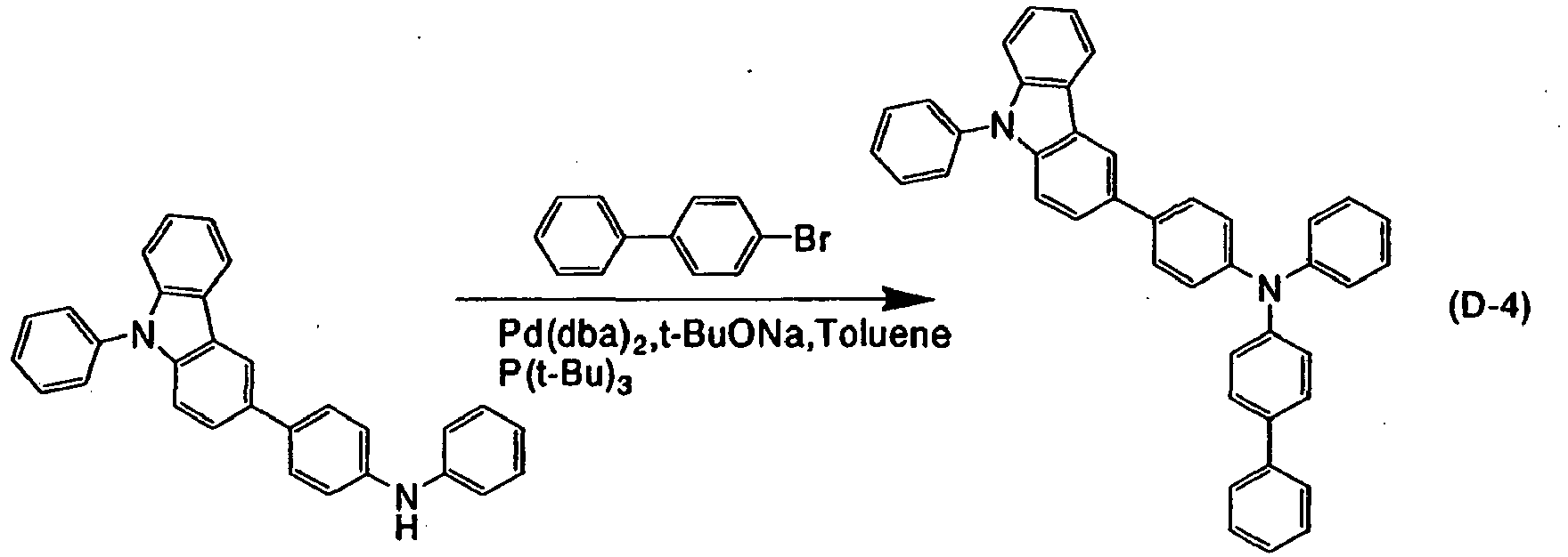
- In a 100-mL three-neck flask, 2.0 g (4.9 mmol) of 4-(9-phenyl-9H-carbazol-3-yl)diphenylamine, 1.1 g (4.9 mmol) of 4-bromobiphenyl, and 2.0 g (20 mmol) of sodium tert-butoxide were put, and the atmosphere in the flask was substituted by nitrogen. Then, 50 mL of toluene and 0.30 mL of tri(tert-butyl)phosphine (10 wt% hexane solution) were added to this mixture.
- This mixture was deaerated while being stirred under low pressure. After the deaeration, 0.10 g of bis(dibenzylideneacetone)palladium(0) was added thereto. Next, this mixture was stirred at 80 °C for 5 hours to be reacted. After the reaction, toluene was added to the reaction mixture, and suction filtration was performed on this suspension through Celite, alumina, and then Florisil to obtain filtrate. The obtained filtrate was washed with a saturated sodium carbonate solution and a saturated saline solution in this order. Magnesium sulfate was added to the organic layer, and the organic layer was dried. After the drying, suction filtration was performed on this mixture to remove the magnesium sulfate; thus, the filtrate was obtained.
- The obtained filtrate was concentrated and purified by silica gel column chromatography. The silica gel column chromatography was performed by, first, using a mixture solvent of toluene: hexane=1:9 as a developing solvent, and then using a mixture solvent of toluene: hexane=3:7 as another developing solvent. A solid which was obtained by concentrating the obtained fraction was recrystallized with a mixture solvent of chloroform and hexane to obtain 2.3 g of a white powder-like solid at a yield of 84 %.
- Sublimation purification of 1.2 g of the obtained white solid was performed by a train sublimation method. The sublimation purification was performed under a reduced pressure of 7.0 Pa, with a flow rate of argon at 3 mL/min, at 280 °C for 20 hours. Accordingly, 1.1 g of the white solid was obtained at a yield of 89 %.
- A compound which was obtained through the
above Step 4 was measured by a nuclear magnetic resonance method (1H NMR). The measurement result is described below, and the 1H NMR chart is shown inFIGS. 10A and 10B . It was found from the measurement result that the carbazole derivative of the present invention, 4-phenyl-4'-(9-phenyl-9H-carbazol-3-yl)triphenylamine (abbreviation: PCBA1BP) represented by the above structural formula (5), was obtained. - 1H NMR (DMSO-d, 300 MHz): δ (ppm) = 7.05-7.20 (m, 7H), 7.28-7.78 (m, 21H), 8.34 (d, J = 7.8 Hz, 1H), 8.57 (s, 1H).
- In addition, an absorption spectrum of a toluene solution of PCBA1BP (abbreviation) is shown in
FIG 11A . In addition, an absorption spectrum of a thin film of PCBA1BP (abbreviation) is shown inFIG. 11B . An ultraviolet-visible spectrophotometer (V-550, manufactured by JASCO Corporation) was used for the measurement. The spectrum of the solution was measured in a quartz cell. The sample of the thin film was fabricated by vapor evaporation of PCBA1BP (abbreviation) over a quartz substrate. The absorption spectrum of the solution which was obtained by subtracting the quartz cell from the measured sample is shown inFIG 11A , and the absorption spectrum of the thin film which was obtained by subtracting the quartz substrate from the measured sample is shown inFIG 11B . - In
FIGS. 11A and 11B , the horizontal axis indicates the wavelength (nm) and the vertical axis indicates the absorption intensity (arbitrary unit). In the case of the toluene solution, an absorption peak was observed at around 335 nm, and in the case of the thin film, an absorption peak was observed at around 341 nm. In addition, an emission spectrum of the toluene solution (excitation wavelength: 346 nm) of PCBA1BP (abbreviation) is shown inFIG. 11A . In addition, an emission spectrum of the thin film (excitation wavelength: 386 nm) of PCBA1BP (abbreviation) is shown inFIG 11B . InFIGS. 11A and 11B , the horizontal axis indicates the wavelength (nm) and the vertical axis indicates the light emission intensity (arbitrary unit). The maximum emission wavelength was 391 nm (excitation wavelength: 346 nm) in the case of the toluene solution and 416 nm (excitation wavelength: 386 nm) in the case of the thin film. - An oxidation-reduction reaction characteristic of PCBA1BP (abbreviation) was examined by a cyclic voltammetry (CV) measurement. An electrochemical analyzer (ALS model 600A or 600C, manufactured by BAS Inc.) was used for the measurement.
- As for a solution used in the CV measurement, dehydrated dimethylformamide (DMF) (manufactured by Aldrich, 99.8%, catalog number: 22705-6) was used as a solvent, and tetra-n-butylammonium perchlorate (n-Bu4NClO4, product of Tokyo Chemical Industry Co., Ltd., catalog No. T0836), which was a supporting electrolyte, was dissolved in the solvent such that the concentration thereof was 100 mmol/L. Further, the object to be measured was also dissolved in the solvent such that the concentration thereof was 2 mmol/L. A platinum electrode (PTE platinum electrode, manufactured by BAS Inc.) was used as a working electrode, another platinum electrode (Pt counter electrode for VC-3 (5 cm), manufactured by BAS Inc.) was used as an auxiliary electrode, and an Ag/Ag+ electrode (RE7 reference electrode for nonaqueous solvent, manufactured by BAS Inc.) was used as a reference electrode. Note that the measurement was performed at room temperature (20 °C to 25 °C). In addition, the scan speed at the CV measurement was 0.1 V/sec.
- First, potential energy (eV) of the reference electrode (Ag/Ag+ electrode) used in
Embodiment 1 with respect to the vacuum level was calculated. That is, the Fermi level of the Ag/Ag+ electrode was calculated. It is known that the oxidation-reduction potential of ferrocene in methanol is +0.610 V [vs. SHE] with respect to a standard hydrogen electrode (Reference: Christian R. Goldsmith et al., J. Am. Chem. Soc., Vol. 124, No. 1, pp.83-96, 2002). On the other hand, the oxidation-reduction potential of ferrocene in methanol measured by using the reference electrode used inEmbodiment 1 was found to be +0.11 V [vs. Ag/Ag+]. Therefore, it was found that the potential energy of the reference electrode used inEmbodiment 1 was less than that of the standard hydrogen electrode by 0.50 [eV]. - Here, it is also known that the potential energy of the standard hydrogen electrode with respect to the vacuum level is (-4.44 eV (Reference: Toshihiro Ohnishi and Tamami Koyama, Macromolecular EL material, Kyoritsu Shuppan, pp.64-67). As described above, the potential energy of the reference electrode used in
Embodiment 1 with respect to the vacuum level was calculated to be -4.44-0.50 = -4.94 [eV]. -
FIG. 41 shows the CV measurement result on the oxidation reaction characteristics. Note that the measurement of the oxidation reaction characteristics was performed by the steps of scanning the potential of the working electrode with respect to the reference electrode in ranges of (1) 0.07 V to 1.00 V, and then (2) 1.00 V to 0.07 V. - First, the calculation of the HOMO level of PCBA1BP (abbreviation) by CV measurement is described in detail. As shown in
FIG 41 , an oxidization peak potential E pa was 0.536 V In addition, a reduction peak potential E pc was 0.446 V Therefore, a half-wave potential (an intermediate potential between E pc and E pa) can be calculated to be 0.49 V. This shows that PCBA1BP (abbreviation) can be oxidized by an electrical energy of 0.49 V [vs. Ag/Ag+], and this energy corresponds to the HOMO level. Here, the potential energy of the reference electrode used inEmbodiment 1 with respect to the vacuum level is -4.94 [eV] as described above. Therefore, the HOMO level of PCBA1BP (abbreviation) was found to be -4.94-0.49 = -5.43 [eV]. In addition, the oxidation peak took a similar value even after the 100 cycles. Accordingly, it was found that repetition of the oxidation reduction between an oxidation state and a neutral state had favorable chracteristics. - In
Embodiment 2, a synthetic method of a carbazole derivative of the present invention, 4,4'-diphenyl-4"-(9-phenyl-9-H-carbazol-3-yl)triphenylamine (abbreviation: PCBBi1BP) represented by a structural formula (6), will be specifically described.
- A synthetic scheme of 4-phenyl-diphenylamine in Step 1-1 is shown in the following (E-1-1).

- In a three-neck flask, 5.2 g (2.5 mmol) of tri-tert-butylphosphine (10 wt% hexane solution) was added to a dehydrated xylene suspension (150 mL) containing 20.0 g (85.8 mmol) of 4-bromobiphenyl, 16.0 g (172 mmol) of aniline, 0.19 g (0.86 mmol) of palladium(II) acetate, and 23.7 g (172 mmol) of potassium carbonate, and a mixture thereof was refluxed under a nitrogen atmosphere at 120 °C for 10 hours. After completion of the reaction, the reaction mixture was washed with water and separated into an organic layer and an aqueous layer, and the aqueous layer was extracted with toluene.
- The above obtained toluene layer was combined with the above organic layer, followed by washing with a saturated saline solution. Then, magnesium sulfate was added thereto to remove moisture in the organic layer. Suction filtration was performed on this mixture to concentrate the obtained filtrate. The obtained residue was purified by silica gel column chromatography (a developing was solvent: toluene). Accordingly, 13.5 g of a white solid of 4-phenyl-diphenylamine, which was obtained by concentrating the obtained solution, was obtained at a yield of 64 %.
- A synthetic scheme of 4,4'-diphenyltriphenylamine in Step 1-2 is shown in the following (E-1-2).

- In a 100-mL three-neck flask, 3.7 g (15 mmol) of 4-phenyl-diphenylamine, 3.5 g (15 mmol) of 4-bromobiphenyl, 2.5 g (25 mmol) of sodium tert-butoxide, and 10 mg (0.02 mmol) of bis(dibenzylideneacetone)palladium(0) were put, and the atmosphere in the flask was substituted by nitrogen. Then, 40 mL of dehydrated xylene was added to this mixture. The mixture was deaerated while being stirred under low pressure. After the deaeration, 0.2 mL (60 mmol) of tri(tert-butyl)phosphine (10 wt% hexane solution) was added thereto.
- Next, this mixture was stirred at 120 °C for 5 hours, to be reacted. After the reaction, toluene was added to the reaction mixture, and suction filtration was performed on this suspension through Celite, alumina, and then Florisil to obtain filtrate. The obtained filtrate was washed with a saturated sodium carbonate solution and a saturated saline solution in this order. Magnesium sulfate was added to the obtained organic layer to remove moisture. Suction filtration was performed on this mixture through Celite, alumina, and then Florisil to concentrate the obtained filtrate. Acetone and methanol were added to the obtained residue, and the residue was irradiated with supersonic and then recrystallized to obtain 5.4 g of a white powder-like solid at a yield of 92 %.
- In addition to Step 1-1 and Step 1-2 which are described above, 4,4'-diphenyltriphenylamine can also be synthesized using a synthetic method shown in Step 1'. Note that a synthetic scheme of 4,4'-diphenyltriphenylamine in Step 1' is shown in the following (E-1').

- In a 200-mL three-neck flask, 1.9 g (20 mmol) of aniline, 9.3 g (40 mmol) of 4-bromobiphenyl, 4.5 g (45 mmol) of sodium tert-butoxide, 0.4 g (2.0 mmol) of palladium(II) acetate, and 1.1 g (2.0 mmol) of 1,1-bis(diphenylphosphino)ferrocene (abbreviation: DPPF) were put, and the atmosphere in the flask was substituted by nitrogen. Then, 70 mL of dehydrated xylene was added to this mixture. This mixture was deaerated while being stirred under low pressure, and the mixture was stirred at 110 °C for 3 hours to be reacted. After the reaction, toluene was added to the reaction mixture, and suction filtration was performed on this suspension through Celite, alumina, and then Florisil to obtain filtrate. The obtained filtrate was washed with a saturated sodium carbonate solution and a saturated saline solution in this order. Magnesium sulfate was added to the obtained organic layer to remove moisture. Suction filtration was performed on this mixture through Celite, alumina, and then Florisil to concentrate the obtained filtrate. Acetone and hexane were added to the obtained residue, and the residue was irradiated with supersonic and then recrystallized to obtain 5.4 g of a white powder-like solid at a yield of 67 %.
- With the use of Step 1-1 and Step 1-2 which are described above, or 4,4'-diphenyltriphenylamine which was synthesized using a synthetic method shown in Step 1', 4-bromo-4',4"-diphenyltriphenylamine is synthesized. Note that a synthetic scheme of 4-bromo-4',4"-diphenyltriphenylamine in
Step 2 is shown in the following (E-2).
- After 4.0 g (10 mmol) of 4,4'-diphenyltriphenylamine was dissolved in a mixture solvent of 50 mL of toluene and 50 mL of ethyl acetate in a conical flask, N-bromo succinimide (abbreviation: NBS) was added to this solution. After that, this mixture was stirred at room temperature for 120 hours. After completion of the reaction, this mixture solution was washed with water, and magnesium sulfate was added thereto to remove moisture. This mixture solution was filtrated and the obtained filtrate was concentrated to perform recrystallization. Accordingly, 4.5 g of an objective white powder was obtained at a yield of 95 %.
- A synthetic scheme of 4,4'-diphenyl-4"-(9-phenyl-9-H-carbazol-3-yl)triphenylamine (abbreviation: PCBBi1BP) in
Step 3 is shown in the following (E-3).
- In a 100-mL three-neck flask, 1.5 g (3.1 mmol) of 4-bromo-4',4"-diphenyltriphenylamine, 0.9 g (3.1 mmol) of 9-phenyl-9H-carbazol-3-boronic acid, 50 mg (0.023 mmol) of palladium(II) acetate, and 0.050 g (0.17 mmol) of tri(o-tolyl)phosphine were put, and the atmosphere in the flask was substituted by nitrogen. Note that since a synthetic method of 9-phenyl-9H-carbazol-3-boronic acid is similar to that described in
Embodiment 1, the description is to be referred thereto; thus, description here is omitted. 30 mL of ethyleneglycoldimethylether (DME) and 15 mL of potassium carbonate solution (2 mol/L) were added to this mixture. This mixture was deaerated while being stirred under low pressure. After the deaeration, this mixture was stirred at 90 °C for 5 hours to be reacted. - After the reaction, ethyl acetate was added to the reaction mixture, and this suspension was washed with a saturated sodium hydrogen carbonate solution and a saturated saline solution. Magnesium sulfate was added to an organic layer, and the organic layer was dried. After the drying, suction filtration was performed on this mixture to remove the magnesium sulfate; thus, filtrate was obtained. Toluene was added to a solid which was obtained by concentrating the obtained filtrate and the mixture was dissolved. Then, suction filtration was performed on this solution through Celite, alumina and Florisil to obtain filtrate. The obtained filtrate was concentrated and purified by silica gel column chromatography. The silica gel column chromatography was performed by, first, using a mixture solvent of toluene: hexane=1:9 as a developing solvent, and then using a mixture solvent of toluene: hexane=3:7 as another developing solvent.
- A solid which was obtained by concentrating the obtained fraction was recrystallized with a mixture solvent of dichloromethane and hexane to obtain 1.3 g of an objective white solid at a yield of 66 %. Sublimation purification of 1.1 g of the obtained white solid was performed by a train sublimation method. The sublimation purification was performed under a reduced pressure of 7.0 Pa, with a flow rate of argon at 4 mL/min, at 305 °C for 15 hours. Accordingly, 840 mg of the white solid was obtained at a yield of 76 %.
- A compound which was obtained through the
above Step 4 was measured by a nuclear magnetic resonance method (1H NMR). The measurement result is described below, and the 1H NMR chart is shown inFIGS. 12A and 12B . It was found from the measurement result that the carbazole derivative of the present invention, 4,4'-diphenyl-4"-(9-phenyl-9-H-carbazol-3-yl)triphenylamine (abbreviation: PCBBi1BP) represented by the above structural formula (6), was obtained. - 1H NMR (CDCl3, 300 MHz): δ (ppm) = 7.25-7.69 (m, 32H), 8.19 (d, J = 7.3 Hz, 1H), 8.35 (s, 1H).
- In addition, an absorption spectrum of a toluene solution of PCBBi1BP (abbreviation) is shown in
FIG. 13A . In addition, an absorption spectrum of a thin film of PCBBi1BP (abbreviation) is shown inFIG. 13B . An ultraviolet-visible spectrophotometer (V-550, manufactured by JASCO Corporation) was used for the measurement. The spectrum of the solution was measured in a quartz cell. The sample of the thin film was fabricated by vapor evaporation of PCBBi1BP (abbreviation) over a quartz substrate. The absorption spectrum of the solution which was obtained by subtracting the quartz cell from the measured sample is shown inFIG. 13A , and the absorption spectrum of the thin film which was obtained by subtracting the quartz substrate from the measured sample is shown inFIG. 13B . InFIGS. 13A and 13B , the horizontal axis indicates the wavelength (nm) and the vertical axis indicates the absorption intensity (arbitrary unit). In the case of the toluene solution, an absorption peak was observed at around 347 nm, and in the case of the thin film, an absorption peak was observed at around 350 nm. In addition, an emission spectrum of the toluene solution (excitation wavelength: 358 nm) of PCBBi1BP (abbreviation) is shown inFIG 13A . In addition, an emission spectrum of the thin film (excitation wavelength: 366 nm) of PCBBi1BP (abbreviation) is shownFIG 13B . InFIGS. 13A and 13B , the horizontal axis indicates the wavelength (nm) and the vertical axis indicates the light emission intensity (arbitrary unit). The maximum emission wavelength was 399 nm (excitation wavelength: 358 nm) in the case of the toluene solution and 417 nm (excitation wavelength: 366 nm) in the case of the thin film. - An oxidation-reduction reaction characteristic of PCBBi1BP (abbreviation) was examined by a cyclic voltammetry (CV) measurement. Since the measurement method is similar to that of
Embodiment 1, the description is omitted. -
FIG 42 shows the CV measurement result on the oxidation reaction characteristics. As shown inFIG. 42 , an oxidization peak potential E pa can be read as 0.521 V, and a reduction peak potential E pc can be read as +0.431 V Therefore, a half-wave potential (an intermediate potential between E pc and E pa) can be calculated to be +0.48 V. According to the calculation similar to that ofEmbodiment 1, the HOMO level of PCBBi1BP (abbreviation) was found to be = -5.42 [eV]. In addition, the oxidation peak took a similar value even after the 100 cycles. Accordingly, it was found that repetition of the oxidation reduction between an oxidation state and a neutral state had favorable characteristics. - The result of measuring the thin film using a photoelectron spectrometer (AC-2, manufactured by Riken Keiki Co., Ltd.) under the atmosphere indicated that the HOMO level of PCBBi1BP (abbreviation) was -5.34 eV. The Tauc plot of the absorption spectrum of the thin film revealed that the absorption edge was 3.15 eV Thus, the energy gap in the solid state was estimated to be 3.15 eV, which means that the LUMO level of PCBBi1BP (abbreviation) is -2.19 eV.
- In addition, the glass transition temperature of PCBBi1BP (abbreviation) was examined with a differential scanning calorimetry (
Pyris 1 DSC, manufactured by Perkin Elmer Co., Ltd.). According to the measurement results, it was found that the glass transition temperature was 123 °C. In this manner, PCBBi1BP (abbreviation) has a high glass transition temperature and favorable heat resistance. In addition, the crystallization peak does not exist; thus, it was found that PCBBi1BP (abbreviation) is a substance which is hard to be crystallized. - In
Embodiment 3, a synthetic method of a carbazole derivative of the present invention,
9,9-dimethyl-N-phenyl-N-[4-(9-phenyl-9H-carbazol-3-yl)phenyl]-fluorene-2-amine (abbreviation: PCBAF) represented by a structural formula (7), will be specifically described.
- A synthetic scheme of 2-bromo-9,9-dimethylfluoren in
Step 1 is shown in the following (F-1).
- In a 500-mL conical flask, 12.5 g (51 mmol) of 2-bromofluorene, 8.5 g (51 mmol) of potassium iodide, 14.3 g (0.50 mol) of potassium hydroxide, and 250 mL of dimethyl sulfoxide were stirred for 30 minutes. Then, 10 mL of methyl iodide was added to this mixture little by little. This mixture was stirred at room temperature for 48 hours. After the reaction, 400 mL of chloroform was added to the reaction solution and this mixture was stirred. This solution was washed with 1N hydrochloric acid, a saturated sodium carbonate solution, and a saturated saline solution in this order. Magnesium sulfate was added to the obtained organic layer to remove moisture.
- This mixture was subjected to suction filtration and concentrated. Then, a residue thereof was purified by silica gel column chromatography. The silica gel column chromatography was performed by, first, using hexane as a developing solvent, and then using a mixture solvent of ethyl acetate: hexane=1:5 as another developing solvent. The corresponding fractions were concentrated and dried to obtain 12 g of a brown oily substance at a yield of 97 %.
- A synthetic scheme of 9,9-dimethyl-N-phenyl-N-[4-(9-phenyl-9H-carbazol-3-yl)phenyl]-fluorene-2-amine (abbreviation: PCBAF) in
Step 2 is shown in the following (F-2).
- In a 100-mL three-neck flask, 2.0 g (4.9 mmol) of 4-(9-phenyl-9H-carbazol-3-yl)diphenylamine (abbreviation: PCBA), 1.3 g (4.9 mmol) of 2-bromo-9,9-dimethylfluoren, and 2.0 g (20 mmol) of sodium tert-butoxide were put, and the atmosphere in the flask was substituted by nitrogen. Note that since a synthetic method of PCBA (abbreviation) is similar to that described in
Embodiment 2, the description is to be referred thereto; thus, description here is omitted. Then, 50 mL of toluene and 0.30 mL of tri(tert-butyl)phosphine (10 wt% hexane solution) were added to this mixture. The mixture was deaerated while being stirred under low pressure. After the deaeration, 0.10 g of bis(dibenzylideneacetone)palladium(0) was added thereto. Next, the mixture was stirred at 80 °C for 5 hours to be reacted. After the reaction, toluene was added to the reaction mixture, and suction filtration was performed on this suspension through Celite, alumina, and then Florisil to obtain filtrate. - The obtained filtrate was concentrated and purified by silica gel column chromatography. The silica gel column chromatography was performed by, first, using a mixture solvent of toluene: hexane=1:9 as a developing solvent, and then using a mixture solvent of toluene: hexane=3:7 as another developing solvent. A solid which was obtained by concentrating the obtained fraction was recrystallized with a mixture solvent of chloroform and hexane to obtain 1.3 g of an objective compound at a yield of 44%.
- Sublimation purification of 1.3 g of the obtained light yellow solid was performed by a train sublimation method. The sublimation purification was performed under a reduced pressure of 7.0 Pa, with a flow rate of argon at 3 mL/min, at 270 °C for 20 hours. Accordingly, 1.0 g of the light yellow solid was obtained at a yield of 77 %.
- A compound which was obtained through the
above Step 2 was measured by a nuclear magnetic resonance method (1H NMR). The measurement result is described below, and the 1H NMR chart is shown inFIGS. 14A and 14B . It was found from the measurement result that the carbazole derivative of the present invention, 9,9-dimethyl-N-phenyl-N-[4-(9-phenyl-9H-carbazol-3-yl)phenyl]-fluorene-2-amine (abbreviation: PCBAF) represented by the above structural formula (7), was obtained. - 1H NMR (DMSO-d, 300 MHz): δ (ppm) = 1.39 (s, 6H) 6.98-7.82 (m, 26H), 8.35 (d, J =6.8 Hz, 1H), 8.57 (s, 1H).
- In addition, an absorption spectrum of a toluene solution of PCBAF (abbreviation) is shown in
FIG. 15A . In addition, an absorption spectrum of a thin film of PCBAF (abbreviation) is shown inFIG 15B . An ultraviolet-visible spectrophotometer (V-550, manufactured by JASCO Corporation) was used for the measurement. The spectrum of the solution was measured in a quartz cell. The sample of the thin film was fabricated by vapor evaporation of PCBAF (abbreviation) over a quartz substrate. The absorption spectrum of the solution which was obtained by subtracting the quartz cell from the measured sample is shown inFIG. 15A , and the absorption spectrum of the thin film which was obtained by subtracting the quartz substrate from the measured sample is shown inFIG. 15B . InFIGS. 15A and 15B , the horizontal axis indicates the wavelength (nm) and the vertical axis indicates the absorption intensity (arbitrary unit). In the case of the toluene solution, an absorption peak was observed at around 339 nm, and in the case of the thin film, an absorption peak was observed at around 345 nm. In addition, an emission spectrum of the toluene solution (excitation wavelength: 347 nm) of PCBAF (abbreviation) is shown inFIG 15A . In addition, an emission spectrum of the thin film (excitation wavelength: 370 nm) of PCBAF (abbreviation) is shownFIG 15B . InFIGS. 15A and 15B , the horizontal axis indicates the wavelength (nm) and the vertical axis indicates the light emission intensity (arbitrary unit). The maximum emission wavelength was 394 nm (excitation wavelength: 347 nm) in the case of the toluene solution and 404 nm (excitation wavelength: 370 nm) in the case of the thin film. - An oxidation-reduction reaction characteristic of PCBAF (abbreviation) was examined by a cyclic voltammetry (CV) measurement. Since the measurement method is similar to that of
Embodiment 1, the description is omitted. -
FIG. 43 shows the CV measurement result on the oxidation reaction characteristics. As shown inFIG 43 , an oxidization peak potential E pa can be read as 0.481 V, and a reduction peak potential E pc can be read as +0.393 V. Therefore, a half-wave potential (an intermediate potential between E pc and E pa) can be calculated to be +0.44 V According to the calculation similar to that ofEmbodiment 1, the HOMO level of PCBAF (abbreviation) was found to be = -5.38 [eV]. In addition, the oxidation peak took a similar value even after the 100 cycles. Accordingly, it was found that repetition of the oxidation reduction between an oxidation state and a neutral state had favorable characteristics. - In
Embodiment 4, a synthetic method of a carbazole derivative of the present invention, N-phenyl-N-[4-(9-phenyl-9H-carbazol-3-yl)phenyl]-spiro-9,9'-bifluoren-2-amine (abbreviation: PCBASF) represented by a structural formula (8), will be specifically described.
- A synthetic scheme of 9-(biphenyl-2-yl)-2-bromofluoren-9-ol in Step 1-1 is shown in the following (G-1-1).

- In a 100-mL three-neck flask to which a dropping funnel and a Dimroth condenser were connected, 1.26 g (0.052 mol) of magnesium was put, and the flask was evacuated. The magnesium was activated by heating and stirring for 30 minutes. After cooling to room temperature, the flask was placed under a nitrogen gas flow. Then, 5 mL of diethyl ether and several drops of dibromoethane were added thereto, and 11.65 g (0.050 mol) of 2-bromobiphenyl dissolved in 15 mL of diethyl ether was slowly dropped from the dropping funnel into the mixture. After completion of the dropping, the mixture was refluxed for 3 hours and made into a Grignard reagent.
- In a 200-mL three-neck flask to which a dropping funnel and a Dimroth condenser were connected, 11.7 g (0.045 mol) of 2-bromo-9-fluorenone and 40 mL of diethyl ether were put. To this reaction solution, the synthesized Grignard reagent was slowly dropped from the dropping funnel. After completion of the dropping, the mixture was refluxed for 2 hours, and then stirred at room temperature overnight. After completion of the reaction, the solution was washed twice with a saturated ammonia chloride solution, and separated into an aqueous layer and an organic layer. The obtained aqueous layer was extracted twice with ethyl acetate, and this ethyl acetate solution and the obtained organic layer were washed with a saturated saline solution. After moisture was removed by magnesium sulfate, suction filtration and concentration were performed to obtain 18.76 g of a solid of 9-(biphenyl-2-yl)-2-bromo-9-fluorenol at a yield of 90 %.
- A synthetic scheme of 2-bromo-spiro-9,9'-bifluoren in Step 1-2 is shown in the following (G-1-2).

- In a 200-mL three-neck flask, 18.76 g (0.045 mol) of the synthesized 9-(biphenyl-2-yl)-2-bromo-9-fluorenol and 100 mL of glacial acetic acid were put, several drops of concentrated hydrochloric acid were added thereto, and the mixture was refluxed for 2 hours. After completion of the reaction, a precipitate was collected by suction filtration, and the precipitate was filtered and washed with a saturated sodium hydrogen carbonate solution and water. The obtained brown solid was recrystallized with ethanol to obtain 10.24 g of a light-brown powder-like solid at a yield of 57%.
- A synthetic scheme of N-phenyl-N-[4-(9-phenyl-9H-carbazol-3-yl)phenyl]-spiro-9,9'-bifluoren-2-amine (abbreviation: PCBASF) in
Step 2 is shown in the following (G-2).
- In a 100-mL three-neck flask, 2.0 g (4.9 mmol) of 4-(9-phenyl-9H-carbazol-3-yl)diphenylamine (abbreviation: PCBA), 1.9 g (4.9 mmol) of 2-bromo-spiro-9,9'-bifluoren, and 2.0 g (20 mmol) of sodium tert-butoxide were put, and the atmosphere in the flask was substituted by nitrogen. Then, 50 mL of toluene and 0.30 mL of tri(tert-butyl)phosphine (10 wt% hexane solution) were added to this mixture. This mixture was deaerated while being stirred under low pressure. After the deaeration, 0.10 g of bis(dibenzylideneacetone)palladium(0) was added thereto.
- Next, this mixture was stirred at 80 °C for 5 hours to be reacted. After the reaction, toluene was added to the reaction mixture, and suction filtration was performed on this suspension through Celite, alumina, and then Florisil to obtain filtrate. The obtained filtrate was washed with a saturated sodium carbonate solution and a saturated saline solution in this order. After magnesium sulfate was added to an organic layer to remove moisture, suction filtration was performed on this mixture and the magnesium sulfate was removed to obtain filtrate. A solid which was obtained by concentrating the obtained filtrate was recrystallized with a mixture solvent of chloroform and hexane to obtain 3.4 g of a white powder-like solid at a yield of 94 %. Sublimation purification of 2.3 g of the obtained white solid was performed by a train sublimation method. The sublimation purification was performed under a reduced pressure of 7.0 Pa, with a flow rate of argon at 3 mL/min, at 310 °C for 20 hours. Accordingly, 1.7 g of the white solid was obtained at a yield of 74 %.
- A compound which was obtained through the
above Step 2 was measured by a nuclear magnetic resonance method (1H NMR). The measurement result is described below, and the 1H NMR chart is shown inFIGS. 16A and 16B . It was found from the measurement result that the carbazole derivative of the present invention, N-phenyl-N-[4-(9-phenyl-9H-carbazol-3-yl)phenyl]-spiro-9,9'-bifluoren-2-amine (abbreviation: PCBASF) represented by the above structural formula (8), was obtained. - 1H NMR (CDCl3, 300 MHz): δ (ppm) = 6.61-6.70 (m, 2H), 6.83 (d, J = 8.3 Hz, 2H), 6.88-7.79 (m, 30H), 8.16 (d, J = 8.3 Hz, 1H), 8.26 (s, 1H).
- In addition, an absorption spectrum of a toluene solution of PCBASF (abbreviation) is shown in
FIG. 17A . In addition, an absorption spectrum of a thin film of PCBASF (abbreviation) is shown inFIG. 17B . An ultraviolet-visible spectrophotometer (V-550, manufactured by JASCO Corporation) was used for the measurement. The spectrum of the solution was measured in a quartz cell. The sample of the thin film was fabricated by vapor evaporation of PCBASF (abbreviation) over a quartz substrate. The absorption spectrum of the solution which was obtained by subtracting the quartz cell from the measured sample is shown inFIG. 17A , and the absorption spectrum of the thin film which was obtained by subtracting the quartz substrate from the measured sample is shown inFIG. 17B . InFIGS. 17A and 17B , the horizontal axis indicates the wavelength (nm) and the vertical axis indicates the absorption intensity (arbitrary unit). In the case of the toluene solution, an absorption peak was observed at around 338 nm, and in the case of the thin film, an absorption peak was observed at around 345 nm. In addition, an emission spectrum of the toluene solution (excitation wavelength: 352 nm) of PCBASF (abbreviation) is shown inFIG. 17A . In addition, an emission spectrum of the thin film (excitation wavelength: 371 nm) of PCBASF (abbreviation) is shownFIG. 17B . InFIGS. 17A and 17B , the horizontal axis indicates the wavelength (nm) and the vertical axis indicates the light emission intensity (arbitrary unit). The maximum emission wavelength was 396 nm (excitation wavelength: 352 nm) in the case of the toluene solution and 427 nm (excitation wavelength: 371 nm) in the case of the thin film. - An oxidation-reduction reaction characteristic of PCBASF (abbreviation) was examined by a cyclic voltammetry (CV) measurement. Since the measurement method is similar to that of
Embodiment 1, the description is omitted. -
FIG 44 shows the CV measurement result on the oxidation reaction characteristics. As shown inFIG 44 , an oxidization peak potential E pa can be read as 0.52 V, and a reduction peak potential E pc can be read as +0.428 V. Therefore, a half-wave potential (an intermediate potential between E pc and E pa) can be calculated to be +0.47 V. According to the calculation similar to that ofEmbodiment 1, the HOMO level of PCBASF (abbreviation) was found to be = -5.41 [eV]. In addition, the oxidation peak took a similar value even after the 100 cycles. Accordingly, it was found that repetition of the oxidation reduction between an oxidation state and a neutral state had favorable characteristics. - In
Embodiment 5, a method for manufacturing a light-emittingelement 2, a light-emittingelement 3, a light-emittingelement 4, and a light-emittingelement 5, which were formed using carbazole derivatives of the present invention that are synthesized inEmbodiments 1 to 4 and measurement results of their element characteristics will be described. The light-emittingelement 2 was formed using 4-phenyl-4'-(9-phenyl-9H-carbazol-3-yl)triphenylamine (abbreviation: PCBA1BP), the light-emittingelement 3 was formed using 4,4'-diphenyl-4"-(9-phenyl-9-H-carbazol-3-yl)triphenylamine (abbreviation: PCBBi1BP), the light-emittingelement 4 was formed using 9,9-dimethyl-N-phenyl-N-[4-(9-phenyl-9H-carbazol-3-yl)phenyl]-fluorene-2-amine (abbreviation: PCBAF), and the light-emittingelement 5 was formed using N-phenyl-N-[4-(9-phenyl-9H-carbazol-3-yl)phenyl]-spiro-9,9'-bifluoren-2-amine (abbreviation: PCBASF). - Note that each element structure of the light-emitting elements in
Embodiment 5 is a structure shown inFIG. 18 , in which a hole-transportinglayer 1512 is formed using the above carbazole derivative of the present invention. In addition, a light-emittingelement 1 which is a comparative light-emitting element is formed using 4,4'-bis[N-(1-naphthyl)-N-phenylamino]biphenyl (abbreviation: NPB) for the hole-transportinglayer 1512. In order to make comparative conditions of the light-emittingelement 1 with each of the light-emittingelements 2 to 5 the same, the light-emittingelement 1 was formed over the same substrates as the light-emittingelements 2 to 5, and the light-emittingelement 1 was compared to the light-emittingelements 2 to 5. A structural formula of an organic compound used inEmbodiment 5 is shown below.

- First, indium tin oxide containing silicon oxide was deposited over a
substrate 1501 which is a glass substrate by a sputtering method to form afirst electrode 1502. The thickness of thefirst electrode 1502 was set to be 110 nm, and the area was set to be 2 mm × 2 mm. - Next, an
EL layer 1503 in which a plurality of layers are stacked over thefirst electrode 1502 was formed. InEmbodiment 5, theEL layer 1503 has a structure in which afirst layer 1511 which is a hole-injecting layer, asecond layer 1512 which is a hole-transporting layer, athird layer 1513 which is a light-emitting layer, afourth layer 1514 which is an electron-transporting layer, and afifth layer 1515 which is an electron-injecting layer are sequentially stacked. - The substrate having the
first electrode 1502 was fixed to a substrate holder provided in a vacuum evaporation apparatus in such a way that the surface of thefirst electrode 1502 faced downward, and then the pressure was reduced to about 10-4 Pa. Then, 4,4'-bis[N-(1-naphthyl)-N-phenylamino]biphenyl (abbreviation: NPB) and molybdenum(VI) oxide were co-evaporated on thefirst electrode 1502, whereby thefirst layer 1511 which is a hole-injecting layer was formed. The evaporation rate was controlled so that the thickness of the first layer which is a hole-injecting layer could be 50 nm and the weight ratio of NPB to molybdenum(VI) oxide could be 4:1 (= NPB : molybdenum oxide). Note that the co-evaporation method is an evaporation method in which evaporation is performed using a plurality of evaporation sources at the same time in one treatment chamber. - Next, a hole-transporting material was deposited over the
first layer 1511 to a thickness of 10 nm by an evaporation method using resistive heating, and thesecond layer 1512 which is a hole-transporting layer was formed. Note that 4,4'-bis[N-(1-naphthyl)-N-phenylamino]biphenyl (abbreviation: NPB) was used in the case of forming the light-emittingelement 1, 4-phenyl-4'-(9-phenyl-9H-carbazol-3-yl)triphenylamine (abbreviation: PCBA1BP) was used in the case of forming the light-emittingelement element 4, and N-phenyl-N-[4-(9-phenyl-9H-carbazol-3-yl)phenyl]-spiro-9,9'-bifluoren-2-amine (abbreviation: PCBASF) were used in the case of forming the light-emittingelement 5. - Next, the
third layer 1513 which is a light-emitting layer was formed over thesecond layer 1512 by an evaporation method using resistive heating. Thethird layer 1513 was formed by co-evaporating 9-[4-(10-phenyl-9-anthryl)phenyl]-9H-carbazole (abbreviation: CzPA) and 4-(10-phenyl-9-anthryl)-4'-(9-phenyl-9H-carbazol-3-yl)triphenylamine (abbreviation: PCBAPA) to a thickness of 30 nm. Here, the evaporation rate was controlled so that the weight ratio of CzPA to PCBAPA could be 1:0.10 (= CzPA : PCBAPA). - Further, tris(8-quinolinolato)aluminum(III) (abbreviation: Alq) was deposited over the
third layer 1513 to be a thickness of 10 nm by an evaporation method using resistive heating. Then, thefourth layer 1514 which is an electron-transporting layer was formed by depositing bathophenanthroline (abbreviation: BPhen) over thethird layer 1513 to a thickness of 20 nm. - Then, the
fifth layer 1515 which is an electron-injecting layer was formed by depositing lithium fluoride (LiF) to a thickness of 1 nm over thefourth layer 1514. - Finally, a
second electrode 1504 was formed by depositing aluminum to a thickness of 200 nm by an evaporation method using resistance heating, and the light-emittingelements 1 to 5 were formed. - The light-emitting
elements 1 to 5 obtained through the process described above were put into a glove box with a nitrogen atmosphere so that the light-emitting elements were sealed without being exposed to atmospheric air. After that, the operating characteristics of these light-emitting elements were measured. Note that the measurement was performed at room temperature (an atmosphere kept at 25 °C). -
FIG 19 shows the current density vs. luminance characteristics of the light-emittingelements FIG 20 shows the voltage vs. luminance characteristics of the light-emittingelements FIG 21 shows the luminance vs. current efficiency characteristics of the light-emittingelements FIG 22 shows the voltage vs. current characteristics of the light-emittingelements - When the drive voltage of the light-emitting
element 2 was 3.4 V, the luminance and the current value were 1277 cd/m2 and 0.79 mA, respectively. It was found that the light-emittingelement 2 using PCBA1BP (abbreviation) for thesecond layer 1512 showed higher luminance, even when the light-emittingelement 2 was compared to the light-emittingelement 1 using NPB for thesecond layer 1512. Further, it was found that the current efficiency was high with respect to the current density or the luminance. - In addition, in the light-emitting
element 2, an emission wavelength derived from PCBAPA which is a blue light-emitting material was observed but an emission wavelength derived from the hole-transporting material was not observed from emission spectrum shown inFIG. 23 . Thus, it was found that favorable carrier balance was realized in the structure of the light-emittingelement 2 using PCBA1BP (abbreviation) of the present invention. -
FIG. 24 shows the results of a continuous lighting test in which the light-emittingelement 2 was continuously lit by constant current driving with the initial luminance set at 1000 cd/m2 (the vertical axis indicates the relative luminance on the assumption that 1000 cd/m2 is 100 %). From the results inFIG 24 , the light-emittingelement 2 exhibits 92% of the initial luminance even after 160 hours, and was found to have a longer lifetime, as compared to the light-emittingelement 1. Thus, a long lifetime light-emitting element can be obtained by applying PCBA1BP (abbreviation) of the present invention. -
FIG 25 shows the current density vs. luminance characteristics of the light-emittingelements FIG 26 shows the voltage vs. luminance characteristics of the light-emittingelements FIG 27 shows the luminance vs. current efficiency characteristics of the light-emittingelements FIG 28 shows the voltage vs. current characteristics of the light-emittingelements - When the drive voltage of the light-emitting
element 3 was 3.4 V, the luminance and the current value were 1328 cd/m2 and 0.78 mA, respectively. It was found that the light-emittingelement 3 using PCBBi1BP (abbreviation) for thesecond layer 1512 showed higher luminance, even when the light-emittingelement 3 was compared to the light-emittingelement 1 using NPB for thesecond layer 1512. Further, it was found that the current efficiency was high with respect to the current density or the luminance. - In addition, in the light-emitting
element 3, an emission wavelength derived from PCBAPA which is a blue light-emitting material was observed but an emission wavelength derived from the hole-transporting material was not observed from emission spectrum shown inFIG 29 . Thus, it was found that favorable carrier balance was realized in the structure of the light-emittingelement 3 using PCBBi1BP (abbreviation) of the present invention. -
FIG 30 shows the current density vs. luminance characteristics of the light-emittingelements FIG 31 shows the voltage vs. luminance characteristics of the light-emittingelements FIG 32 shows the luminance vs. current efficiency characteristics of the light-emittingelements FIG 33 shows the voltage vs. current characteristics of the light-emittingelements - When the drive voltage of the light-emitting
element 4 was 3.8 V, the luminance and the current value were 1328cd/m2 and 1.08 mA, respectively. It was found that the light-emittingelement 4 using PCBAF (abbreviation) for thesecond layer 1512 showed higher luminance, even when the light-emittingelement 4 was compared to the light-emittingelement 1 using NPB for thesecond layer 1512. - In addition, in the light-emitting
element 4, an emission wavelength derived from PCBAPA which is a blue light-emitting material was observed but an emission wavelength derived from the hole-transporting material was not observed from emission spectrum shown inFIG 34 . Thus, it was found that favorable carrier balance was realized in the structure of the light-emittingelement 4 using PCBAF (abbreviation) of the present invention. -
FIG. 35 shows the results of a continuous lighting test in which the light-emittingelement 4 was continuously lit by constant current driving with the initial luminance set at 1000 cd/m2 (the vertical axis indicates the relative luminance on the assumption that 1000 cd/m2 is 100 %). From the results inFIG 35 , the light-emittingelement 4 exhibits 92% of the initial luminance even after 160 hours and was found to have a longer lifetime, as compared to the light-emittingelement 1. Thus, a long lifetime light-emitting element can be obtained by applying PCBAF (abbreviation) of the present invention. -
FIG. 36 shows the current density vs. luminance characteristics of the light-emittingelements FIG 37 shows the voltage vs. luminance characteristics of the light-emittingelements FIG 38 shows the luminance vs. current efficiency characteristics of the light-emittingelements FIG 39 shows the voltage vs. current characteristics, of the light-emittingelements - When the drive voltage of the light-emitting
element 5 was 3.8 V, the luminance and the current value were 1398 cd/m2 and 1.11 mA, respectively. It was found that the light-emittingelement 5 using PCBASF (abbreviation) for thesecond layer 1512 showed higher luminance, even when the light-emittingelement 5 was compared to the light-emittingelement 1 using NPB for thesecond layer 1512. Further, it was found that the current efficiency was high with respect to the current density or the luminance. - In addition, in the light-emitting
element 5, an emission wavelength derived from PCBAPA which is a blue light-emitting material was observed but an emission wavelength derived from the hole-transporting material was not observed from emission spectrum shown inFIG 40 . Thus, it was found that favorable carrier balance was realized in the structure of the light-emittingelement 5 using PCBASF (abbreviation) of the present invention. - As described above, it was found that the light-emitting
elements 2 to 5 which were formed using the carbazole derivatives of the present invention exhibited an equivalent level of efficiency to the light-emittingelement 1. Thus, it was found that a light-emitting element having high efficiency can be obtained by applying the present invention. - In addition, as another structure of the light-emitting
element 1 shown inEmbodiment 5, PCBA1BP (abbreviation) was used instead of NPB (abbreviation), which was used at the time of forming thefirst layer 1511, and was co-evaporated with molybdenum(VI) oxide to form thefirst layer 1511. With the efficiency, the drive voltage at a luminance of about 1000 cd/m2, and the reliability of such a light-emittingelement 1, favorable values equivalent to those of a light-emittingelement 8 were obtained. The light-emittingelement 8 will be formed inEmbodiment 10 by using a co-evaporation film of NPB and molybdenum(VI) oxide for a hole-injecting layer and using PCBBiNB (abbreviation) for a hole-transporting layer. When the drive voltage of the light-emittingelement 1 was 3.8 V, the luminance and the current value were 949 cd/m2 and 0.65 mA, respectively, and the light-emittingelement 1 exhibited 64 % of the initial luminance when driven for 1500 hours. - As thus described, it was found that PCBA1BP (abbreviation) was a favorable material also as a hole-injecting material. In addition, it was found that favorable characteristics can also be obtained by using the co-evaporation film with molybdenum(VI) oxide for the hole-injecting layer.
- In addition, as another structure of the light-emitting
element 2 shown inEmbodiment 5, PCBA1BP (abbreviation) was used instead of NPB (abbreviation), which was used at the time of forming thefirst layer 1511, and was co-evaporated with molybdenum(VI) oxide to form thefirst layer 1511. With the efficiency, the drive voltage at a luminance of about 1000 cd/m2, and the reliability of such a light-emittingelement 2, favorable values equivalent to those of a light-emittingelement 8 were obtained. The light-emittingelement 8 will be formed inEmbodiment 10 by using a co-evaporation film of NPB and molybdenum(VI) oxide for a hole-injecting layer and using PCBBiNB (abbreviation) for a hole-transporting layer. When the drive voltage of the light-emittingelement 2 was 3.6 V, the luminance and the current value were 843 cd/m2 and 0.53 mA, respectively, and the light-emittingelement 2 exhibited 65 % of the initial luminance when driven for 1500 hours. - As thus described, it was found that PCBA1BP (abbreviation) was a favorable material which can be used for both the
first layer 1511 which is a hole-injecting layer and thesecond layer 1512 which is a hole-transporting layer at the same time. Accordingly, an element could be manufactured easily and material use efficiency could also be improved. - In
Embodiment 6, a synthetic method of a carbazole derivative of the present invention, (biphenyl-4-yl)(phenyl)[4'-(9-phenyl-9H-carbazol-3-yl)biphenyl-4-yl]amine (abbreviation: PCTA1BP) represented by a structural formula (15), will be specifically described.
- A synthetic scheme of 4-[N-(biphenyl-4-yl)-N-phenyl]aminophenylboronic acid in
Step 1 is shown in the following (H-1).
- In a 300-mL three-neck flask, 7.0 g (18 mmol) of 4-bromo-4'-phenyltriphenylamine was put, and the atmosphere in the flask was substituted by nitrogen. Then, 80 mL of tetrahydrofuran (abbreviation: THF) was added thereto, and the mixture was stirred at -78 °C for 10 minutes. After that, 13 mL (21 mmol) of an n-butyllithium hexane solution (1.63 mol/L) was dropped onto this solution from a syringe, and the solution was stirred at -78 °C for 1 hour. After the stirring, 3.5 mL (31 mmol) of trimethyl borate was added to the reaction mixture, and the mixture was stirred at -78 °C for 1 hour and at room temperature for 24 hours. After the reaction, 100 mL of 1M dilute hydrochloric acid was added to the reaction solution, and the mixture was stirred at room temperature for 1 hour. After the stirring, this solution was extracted with ethyl acetate, and an organic layer was washed with a saturated saline solution. After the washing, magnesium sulfate was added to the organic layer, and the organic layer was dried. After the drying, magnesium sulfate was removed by suction filtration to obtain filtrate. The obtained filtrate was concentrated and recrystallized with a mixture solvent of chloroform and hexane to obtain 3.6 g of an object at a yield of 56 %.
- A synthetic scheme of (biphenyl-4-yl)(phenyl)[4'-(9-phenyl-9H-carbazol-3-yl)biphenyl-4-yl]amine in
Step 2 is shown in the following (H-2).
- In a 100-mL three-neck flask, 2.2 g (5.5 mmol) of 4-[N-(biphenyl-4-yl)-N-phenyl]aminophenylboronic acid, 2.0 g (5.5 mmol) of 3-(4-bromophenyl)-9-phenyl-9H-carbazole, 10 mg (0.045 mmol) of palladium(II) acetate, and 0.69 g (0.23 mmol) of tri(o-tolyl)phosphine were put, and 10 mL of a potassium carbonate solution (2.0 mol/L) and 20 mL of ethylene glycol dimethyl ether (abbreviation: DME) were added thereto. This mixture was deaerated while being stirred under low pressure, and the atmosphere in the flask was substituted by nitrogen. This mixture was stirred at 90 °C for 5 hours. After the stirring, toluene was added to the reaction mixture, and the mixture was heated at 90 °C.
- After the heating, this suspension was separated into an organic layer and an aqueous layer. After the separation, the organic layer was washed with a saturated sodium hydrogen carbonate solution and a saturated saline solution. Magnesium sulfate was added to the organic layer, and the organic layer was dried. Suction filtration was performed on this mixture through Celite, alumina, and then Florisil to obtain filtrate. The obtained filtrate was concentrated to obtain a solid. The obtained filtrate was dissolved and purified by silica gel column chromatography. The silica gel column chromatography was performed by, first, using a mixture solvent of toluene: hexane=1:9 as a developing solvent, and then using a mixture solvent of toluene: hexane=2:3 as another developing solvent. A solid which was obtained by concentrating the obtained fraction was dissolved in chloroform and purified by high performance liquid chromatography (HPLC) (developing solvent, chloroform). A solid which was obtained by concentrating the obtained fraction was recrystallized with a mixture solvent of chloroform and hexane to obtain 1.7 g of an objective white solid at a yield of 48 %.
- Sublimation purification of 1.0 g of the obtained white solid was performed by a train sublimation method. The sublimation purification was performed under a reduced pressure of 7.0 Pa, with a flow rate of argon at 4 mL/min, at 300 °C for 15 hours to obtain 0.62 g of the white solid at a yield of 62 %.
- A compound which was obtained through the
above Step 2 was measured by a nuclear magnetic resonance method (1H NMR). The measurement result is described below, and the 1H NMR chart is shown inFIGS. 45A and 45B . It was found from the measurement result that the carbazole derivative of the present invention, PCTA1BP (abbreviation) represented by the above structural formula (15), was obtained. 1H NMR (CDCl3, 300 MHz): δ (ppm) = 7.02-7.79 (m, 32H), 8.19 (d, J = 7.3 Hz, 1H), 8.39 (s, 1H). - In addition, an absorption spectrum of PCTA1BP (abbreviation) (measurement range: 200 nm to 800 nm) was measured. In the case of the toluene solution, an absorption peak on a long wavelength side was observed at around 349 nm, and in the case of the thin film, an absorption peak on a long wavelength side was observed at around 357 nm.
- In addition, an emission spectrum of PCTA1BP (abbreviation) (measurement range: 370 nm to 550 nm) was measured. In the case of the toluene solution, a maximum emission wavelength was 405 nm (excitation wavelength: 320 nm), and in the case of the thin film, a maximum emission wavelength was 420 nm (excitation wavelength: 284 nm). Since the measurement method of an absorption spectrum and an emission spectrum is similar to that of
Embodiment 1, the description is omitted. - The result of measuring the thin film using a photoelectron spectrometer (AC-2, manufactured by Riken Keiki Co., Ltd.) under the atmosphere indicated that the HOMO level of PCTA1BP (abbreviation) was -5.49 eV. The Tauc plot of the absorption spectrum of the thin film revealed that the absorption edge was 3.10 eV. Thus, the energy gap in the solid state was estimated to be 3.10 eV, which means that the LUMO level of PCTA1BP (abbreviation) is -2.39 eV.
- An oxidation-reduction reaction characteristic of PCTA1BP (abbreviation) was examined by a cyclic voltammetry (CV) measurement. Since the measurement method is similar to that of
Embodiment 1, the description is omitted. According to the calculation similar to that ofEmbodiment 1, the HOMO level of PCTA1BP (abbreviation) was found to be = -5.48 [eV]. In addition, the oxidation peak took a similar value even after the 100 cycles. Accordingly, it was found that repetition of the oxidation reduction between an oxidation state and a neutral state had favorable characteristics. - In addition, the glass transition temperature of PCTA1BP (abbreviation) was examined with a differential scanning calorimetry (
Pyris 1 DSC, manufactured by Perkin Elmer Co., Ltd.). According to the measurement results, it was found that the glass transition temperature was 118 °C. In this manner, PCTA1BP (abbreviation) has a high glass transition temperature and favorable heat resistance. In addition, the crystallization peak does not exist; thus, it was found that PCTA1BP (abbreviation) is a substance which is hard to be crystallized. - Note that with the efficiency, the drive voltage at a luminance of about 1000 cd/m2, and the reliability of a light-emitting element formed using PCTA1BP (abbreviation) which was synthesized in
Embodiment 6 in a manner similar to that ofEmbodiment 5 for a hole-transporting layer, favorable values equivalent to those of a light-emittingelement 8 which will be formed using PCBBiNB inEmbodiment 10 were obtained. When the drive voltage of the light-emitting element was 3.6 V, the luminance and the current value were 1044 cd/m2 and 0.67 mA, respectively, and the light-emitting element exhibited 52 % of the initial luminance when driven for 1100 hours. - In
Embodiment 7, a synthetic method of a carbazole derivative of the present invention, bis(biphenyl-4-yl)[4'-(9-phenyl-9H-carbazol-3-yl)biphenyl-4-yl]amine (abbreviation: PCTBi1BP) represented by a structural formula (190), will be specifically described.
- A synthetic scheme of 4-[bis(biphenyl-4-yl)amino]phenylboronic acid in
Step 1 is shown in the following (I-1).
- In a 300-mL three-neck flask, 6.0 g (13 mmol) of 4-bromo-4',4"-diphenyltriphenylamine was put, and the atmosphere in the flask was substituted by nitrogen. Then, 80 mL of tetrahydrofuran (abbreviation: THF) was added thereto, and the mixture was stirred at -78 °C for 10 minutes. After that, 10 mL of an n-butyllithium hexane solution (1.63 mol/L) was dropped onto this solution from a syringe, and the solution was stirred at -78 °C for 1 hour. After the stirring, 2.8 mL (25 mmol) of trimethyl borate was added to the reaction mixture, and the mixture was stirred at -78 °C for 1 hour and further at room temperature for 24 hours. After the stirring, about 50 mL of dilute hydrochloric acid was added to the reaction mixture, and the mixture was stirred at room temperature for 30 minutes. After the stirring, ethyl acetate was added to this mixture to perform extraction. After the extraction, an organic layer was washed with a saturated saline solution. Then, magnesium sulfate was added to the organic layer, and the organic layer was dried. After the drying, suction filtration was performed on this mixture to obtain filtrate. The obtained filtrate was concentrated and recrystallized with a mixture solvent of chloroform and hexane to obtain 4.8 g of an objective white powder-like solid at a yield of 86 %.
- A synthetic scheme of bis(biphenyl-4-yl)[4'-(9-phenyl-9H-carbazol-3-yl)biphenyl-4-yl]amine in
Step 2 is shown in the following (I-2).
- In a 100-mL three-neck flask, 2.0 g (4.5 mmol) of 4-[bis(biphenyl-4-yl)amino]phenylboronic acid, 1.8 g (4.5 mmol) of 3-(4-bromophenyl)-9-phenyl-9H-carbazole, 10 mg (0.045 mmol) of palladium(II) acetate, and 0.69 g (0.23 mmol) of tri(o-tolyl)phosphine were put, and 10 mL of a potassium carbonate solution (2.0 mol/L) and 20 mL of ethylene glycol dimethyl ether (abbreviation: DME) were added thereto. This mixture was deaerated while being stirred under low pressure, and the atmosphere in the flask was substituted by nitrogen. This mixture was stirred at 90 °C for 5 hours. After the stirring, toluene was added to the reaction mixture, and the mixture was heated at 90 °C.
- After the heating, this suspension was separated into an organic layer and an aqueous layer. After the separation, the organic layer was washed with a saturated sodium hydrogen carbonate solution and a saturated saline solution. Magnesium sulfate was added to the organic layer, and the organic layer was dried. Suction filtration was performed on this mixture through Celite, alumina, and then Florisil to obtain filtrate. The obtained filtrate was concentrated to obtain a solid. The obtained filtrate was dissolved in toluene and purified by silica gel column chromatography. The silica gel column chromatography was performed by using toluene as a developing solvent. A solid which was obtained by concentrating the obtained fraction was recrystallized with a mixture solvent of toluene and hexane to obtain 2.4 g of an objective white solid at a yield of 74 %.
- Sublimation purification of the obtained white solid was performed by a train sublimation method. The sublimation purification was performed under a reduced pressure of 7.0 Pa, with a flow rate of argon at 3 mL/min, at 340 °C for 20 hours to obtain 0.70 g of the white solid, the theoretical yield of which is 1.5 g, at a yield of 46%.
- A compound which was obtained through the
above Step 2 was measured by a nuclear magnetic resonance method (1H NMR). The measurement result is described below, and the 1H NMR chart is shown inFIGS. 46A and 46B . It was found from the measurement result that the carbazole derivative of the present invention, PCTBi1BP (abbreviation) represented by the above structural formula (190), was obtained. 1H NMR (CDCl3, 300 MHz): δ (ppm) = 7.18-7.83 (m, 36H), 8.21 (d, J = 7.3 Hz, 1H), 8.40 (s, 1H). - In addition, an absorption spectrum of PCTBi1BP (abbreviation) (measurement range: 200 nm to 800 nm) was measured. In the case of the toluene solution, an absorption peak on a long wavelength side was observed at around 350 nm, and in the case of the thin film, an absorption peak on a long wavelength side was observed at around 357 nm.
- In addition, an emission spectrum of PCTBi1BP (abbreviation) (measurement range: 370 nm to 550 nm) was measured. In the case of the toluene solution, a maximum emission wavelength was 410 nm (excitation wavelength: 320 nm), and in the case of the thin film, a maximum emission wavelength was 447 mm (excitation wavelength: 340 nm). Since the measurement method of an absorption spectrum and an emission spectrum is similar to that of
Embodiment 1, the description is omitted. - The result of measuring the thin film using a photoelectron spectrometer (AC-2, manufactured by Riken Keiki Co., Ltd.) under the atmosphere indicated that the HOMO level of PCTBi1BP (abbreviation) was -5.50 eV. The Tauc plot of the absorption spectrum of the thin film revealed that the absorption edge was 3.14 eV. Thus, the energy gap in the solid state was estimated to be 3.14 eV, which means that the LUMO level of PCTBi1BP (abbreviation) is -2.36 eV.
- An oxidation-reduction reaction characteristic of PCTBi1BP (abbreviation) was examined by a cyclic voltammetry (CV) measurement. Since the measurement method is similar to that of
Embodiment 1, the description is omitted. - According to the calculation similar to that of
Embodiment 1, the HOMO level of PCTBi1BP (abbreviation) was found to be = -5.46 [eV]. In addition, the oxidation peak took a similar value even after the 100 cycles. Accordingly, it was found that repetition of the oxidation reduction between an oxidation state and a neutral state had favorable characteristics. - In addition, the glass transition temperature of PCTBi1BP (abbreviation) was examined with a differential scanning calorimetry (
Pyris 1 DSC, manufactured by Perkin Elmer Co., Ltd.). According to the measurement results, it was found that the glass transition temperature was 133 °C. In this manner, PCTBi1BP (abbreviation) has a high glass transition temperature and favorable heat resistance. In addition, the crystallization peak does not exist; thus, it was found that PCTBi1BP (abbreviation) is a substance which is hard to be crystallized. - Note that with the efficiency, the drive voltage at a luminance of about 1000 cd/m2, and the reliability of a light-emitting element formed using PCTBi1BP (abbreviation) which was synthesized in
Embodiment 7 in a manner similar to that ofEmbodiment 5 for a hole-transporting layer, favorable values equivalent to those of a light-emittingelement 8 which will be formed using PCBBiNB inEmbodiment 10 were obtained. When the drive voltage of the light-emitting element was 3.6 V, the luminance and the current value were 873 cd/m2 and 0.56 mA, respectively, and the light-emitting element exhibited 80 % of the initial luminance when driven for 110 hours. - In
Embodiment 8, a synthetic method of a carbazole derivative of the present invention, 4-(1-naphthyl)-4'-(9-phenyl-9H-carbazol-3-yl)-triphenylamine (abbreviation: PCBANB) represented by a structural formula (343), will be specifically described.
- A synthetic scheme of 3-(4-bromophenyl)-9-phenyl-9H-carbazole in
Step 1 is shown in the following (J-1).
- In a 200-mL three-neck flask, 3.7 g (9.9 mmol) of 3-iodo-9-phenyl-9H-carbazole, 2.0 g (9.9 mmol) of 4-bromo phenylboronic acid, and 0.61 g (2.0 mmol) of tri(o-tolyl)phosphine were put, and 50 mL of ethylene glycol dimethyl ether (abbreviation: DME) and 10 mL of a potassium carbonate solution (2 mol/L) were added to this mixture. This mixture was deaerated while being stirred under low pressure, and the atmosphere in the flask was substituted by nitrogen after the deaeration.
- Then, 0.11 g (0.50 mmol) of palladium(II) acetate was added to this mixture. This mixture was stirred at 80 °C for 9.5 hours. After the stirring, this mixture was cooled to room temperature and then washed twice with water. The obtained aqueous layer was extracted twice with toluene. Then, the extracted solution was combined with an organic layer, followed by washing with a saturated saline solution. The organic layer was dried with magnesium sulfate, this mixture was naturally filtrated, and then the filtrate was concentrated.
- The obtained oily substance was dissolved in about 20 mL of toluene, and suction filtration was performed on this solution through Celite, alumina, and then Florisil. A solid which was obtained by concentrating the obtained filtrate was purified by silica gel column chromatography (developing solvent, toluene: hexane = 1:4) to obtain 1.9 g of an objective white powder-like solid at a yield of 49 %.
- A synthetic scheme of 4-(1-naphthyl)diphenylamine in
Step 2 is shown in the following (J-2).
- In a 200-mL three-neck flask, 12 g (50 mmol) of 4-bromodiphenylamine, 8.6 g (50 mmol) of 1-naphthaleneboronic acid, 22 mg (0.1 mmol) of palladium(II) acetate, and 60 mg (0.2 mmol) of tri(o-tolyl)phosphine were put, and 50 mL of toluene, 20 mL of ethanol, and 35 mL of a potassium carbonate solution (2 mol/L) were added to this mixture. This mixture was deaerated while being stirred under low pressure. After the deaeration, the mixture was stirred under a nitrogen atmosphere at 90 °C for 2 hours to be reacted.
- After the reaction, 100 mL of toluene was added to this reaction mixture, and this suspension was filtrated through Florisil and then Celite. The obtained filtrate was washed with water. Then, magnesium sulfate was added to remove moisture. This suspension was concentrated and purified by silica gel column chromatography (developing solvent, toluene: hexane: ethyl acetate = 1:8:1). The obtained fraction was concentrated, and methanol was added thereto. The mixture was irradiated with supersonic and then recrystallized to obtain 3.0 g of an objective white powder at a yield of 20 %.
- A synthetic scheme of 4-(1-naphthyl)-4'-(9-phenyl-9H-carbazol-3-yl)-triphenylamine in
Step 3 is shown in the following (J-3).
- In a 50-mL three-neck flask, 1.2 g (3.0 mmol) of 3-(4-bromophenyl)-9-phenyl-9H-carbazole, 0.9 g (3.0 mmol) of 4-(1-naphthyl)diphenylamine, 0.5 g (5.0 mmol) of sodium tert-butoxide, and 6.0 mg (0.01 mmol) of bis(dibenzylideneacetone)palladium(0) were put, and 15 mL of dehydrated xylene was added to this mixture. This mixture was deaerated while being stirred under low pressure. After the deaeration, 0.06 mL (0.03 mmol) of tri(tert-butyl)phosphine (10 wt% hexane solution) was added thereto. This mixture was stirred under a nitrogen atmosphere at 120 °C for 4.5 hours to be reacted.
- After the reaction, 250 mL of toluene was added to this reaction mixture, and this suspension was filtrated through Florisil, silica gel, alumina, and then Celite. The obtained filtrate was washed with water. Then, magnesium sulfate was added to remove moisture. This suspension was filtrated through Florisil, alumina, silica gel, and then Celite to obtain filtrate. The obtained filtrate was concentrated, and acetone and methanol were added thereto. The mixture was irradiated with supersonic and then recrystallized to obtain 1.5 g of an objective white powder at a yield of 82 %.
- An Rf value of the objective substance by a silica gel thin layer chromatography (TLC) (developing solvent, ethyl acetate: hexane = 1:10) was 0.34, that of 3-(4-bromophenyl)-9-phenyl-9H-carbazole was 0.46, and that of 4-(1-naphthyl)diphenylamine was 0.25.
- A compound which was obtained through the
above Step 3 was measured by a nuclear magnetic resonance method (1H NMR). The measurement result is described below, and the 1H NMR chart is shown inFIGS. 47A and 47B . It was found from the measurement result that the carbazole derivative of the present invention, PCBANB (abbreviation) represented by the above structural formula (343), was obtained. 1H NMR (CDCl3, 300 MHz): δ (ppm) = 7.07 (t, J = 6.6 Hz, 1H), 7.25-7.67 (m, 26H), 7.84 (d, J = 7.8 Hz, 1H), 7.89-7.92 (m, 1H), 8.03-8.07 (m, 1H), 8.18 (d, J = 7.8 Hz, 1H), 8.35 (d, J = 0.9 Hz, 1H). - In addition, an absorption spectrum of PCBANB (abbreviation) (measurement range: 200 nm to 800 nm) was measured. In the case of the toluene solution, an absorption peak on a long wavelength side was observed at around 335 nm, and in the case of the thin film, an absorption peak on a long wavelength side was observed at around 341 nm.
- In addition, an emission spectrum of PCBANB (abbreviation) (measurement range: 370 nm to 550 nm) was measured. In the case of the toluene solution, a maximum emission wavelength was 410 nm (excitation wavelength: 345 nm), and in the case of the thin film, a maximum emission wavelength was 433 nm (excitation wavelength: 341 nm).
- Since the measurement method of an absorption spectrum and an emission spectrum is similar to that of
Embodiment 1, the description is omitted. - The result of measuring the thin film using a photoelectron spectrometer (AC-2, manufactured by Riken Keiki Co., Ltd.) under the atmosphere indicated that the HOMO level of PCBANB (abbreviation) was -5.44 eV. The Tauc plot of the absorption spectrum of the thin film revealed that the absorption edge was 3.25 eV Thus, the energy gap in the solid state was estimated to be 3.25 eV, which means that the LUMO level of PCBANB (abbreviation) is -2.19 eV.
- An oxidation-reduction reaction characteristic of PCBANB (abbreviation) was examined by a cyclic voltammetry (CV) measurement. Since the measurement method is similar to that of
Embodiment 1, the description is omitted. - According to the calculation similar to that of
Embodiment 1, the HOMO level of PCBANB (abbreviation) was found to be = -5.44 [eV]. In addition, the oxidation peak took a similar value even after the 100 cycles. Accordingly, it was found that repetition of the oxidation reduction between an oxidation state and a neutral state had favorable characteristics. - In addition, the glass transition temperature of PCBANB (abbreviation) was examined with a differential scanning calorimetry (
Pyris 1 DSC, manufactured by Perkin Elmer Co., Ltd.). According to the measurement results, it was found that the glass transition temperature was 115 °C. In this manner, PCBANB (abbreviation) has a high glass transition temperature and favorable heat resistance. In addition, the crystallization peak does not exist; thus, it was found that PCBANB (abbreviation) is a substance which is hard to be crystallized. - In addition,
FIGS. 56 to 59 show the measurement results in element characteristics of the light-emittingelement 6 which was formed using, for a hole-transporting layer, PCBANB (abbreviation) which is the carbazole derivative of the present invention that was synthesized inEmbodiment 8 in a manner similar to that ofEmbodiment 5. It was found that the hole-transporting material of the present invention which was used for the light-emittingelement 6 showed higher luminance, even when the hole-transporting material of the present invention which was used for the light-emittingelement 6 was compared to NPB of the light-emittingelement 1. Note that the light-emittingelement 1 which is a comparative light-emitting element was formed using 4,4'-bis[N-(1-naphthyl)-N-phenylamino]biphenyl (abbreviation: NPB) for the hole-transporting layer 151 in a manner similar to that ofEmbodiment 5. - In addition, in the light-emitting
element 6, an emission wavelength derived from PCBAPA which is a blue light-emitting material was observed but an emission wavelength derived from the hole-transporting material was not observed from emission spectrum shown inFIG. 59 . Thus, it was found that the hole-transporting material of the present invention realizes favorable carrier balance in the structure of the light-emittingelement 6. -
FIG 60 shows the result of a continuous lighting test in which the light-emittingelement 6 was continuously lit by constant current driving with the initial luminance set at 1000 cd/m2 (the vertical axis indicates the relative luminance on the assumption that 1000 cd/m2 is 100 %). From the results inFIG 60 , the light-emittingelement 6 was found to have a longer lifetime, as compared to the light-emittingelement 1. Thus, a long lifetime light-emitting element can be obtained by applying the present invention. - In
Embodiment 9, a synthetic method of a carbazole derivative of the present invention, 4,4'-di(1-naphthyl)-4"-(9-phenyl-9H-carbazol-3-yl)-triphenylamine (abbreviation: PCBNBB) represented by a structural formula (229), will be specifically described.
- A synthetic scheme of 4,4'-dibromotriphenylamine in
Step 1 is shown in the following (K-1).
- After 12 g (50 mmol) of triphenylamine was dissolved in a mixture solvent of 250 mL of ethyl acetate in a 500-mL conical flask, 18 g (100 mmol) of N-bromo succinimide (abbreviation: NBS) was added to this solution. After that, this mixture was stirred at room temperature for 24 hours. After completion of the reaction, this mixture solution was washed with water, and magnesium sulfate was added thereto to remove moisture. This mixture solution was filtrated and the obtained filtrate was concentrated and dried to obtain 20 g of an objective white solid at a yield of 99 %.
- A synthetic scheme of 4,4'-di(1-naphthyl)triphenylamine in
Step 2 is shown in the following (K-2).
- In a 100-mL three-neck flask, 6.0 g (15 mmol) of 4,4'-dibromotriphenylamine, 5.2 g (30 mmol) of 1-naphthaleneboronic acid, 2.0 mg (0.01 mmol) of palladium(II) acetate, and 6.0 mg (0.02 mmol) of tri(o-tolyl)phosphine were put, and 20 mL of toluene, 5 mL of ethanol, and 20 mL of a potassium carbonate solution (2 mol/L) were added to this mixture. This mixture was deaerated while being stirred under low pressure. After the deaeration, the mixture was stirred under a nitrogen atmosphere at 90 °C for 4.5 hours to be reacted.
- After the reaction, 150 mL of toluene was added to this reaction mixture, and on this suspension was filtrated through Florisil and then Celite. The obtained filtrate was washed with water. Then, magnesium sulfate was added to remove moisture. This suspension was filtrated through Florisil, alumina, silica gel, and then Celite to obtain filtrate. The obtained filtrate was concentrated, and methanol was added thereto. The mixture was irradiated with supersonic and then recrystallized to obtain 6.4 g of an objective white powder at a yield of 86 %.
- An Rf value of the objective substance by a silica gel thin layer chromatography (TLC) (developing solvent, ethyl acetate: hexane = 1:10) was 0.53 and that of 4,4'-dibromotriphenylamine was 0.69.
- A synthetic scheme of 4-bromo-4',4"-di(1-naphthyl)triphenylamine in
Step 3 is shown in the following (K-3).
- After 6.4 g (13 mmol) of 4,4'-di(1-naphthyl)triphenylamine was dissolved in 150 mL of ethyl acetate in a 300-mL conical flask, 2.3 g (13 mmol) of N-bromo succinimide (abbreviation: NBS) was added to this solution. After that, this mixture was stirred at room temperature for 24 hours. After completion of the reaction, this mixture solution was washed with water, and magnesium sulfate was added thereto to remove moisture. This mixture solution was filtrated, the obtained filtrate was concentrated, and methanol was added thereto. The mixture was irradiated with supersonic and then recrystallized to be purified by silica gel column chromatography (developing solvent, toluene: hexane = 1:5). Accordingly, 1.6 g of an objective white powder was obtained at a yield of 22 %.
- A synthetic scheme of 4,4'-di(1-naphthyl)-4"-(9-phenyl-9H-carbazol-3-yl)-triphenylamine in
Step 4 is shown in the following (K-4).
- In a 50-mL three-neck flask, 1.4 g (2.5 mmol) of 4-bromo-4',4"-di(1-naphthyl)triphenylamine, 0.7 g (2.5 mmol) of 9-phenyl-9H-carbazol-3-yl-boronic acid, 4.0 mg (0.02 mmol) of palladium(II) acetate, and 6.0 mg (0.02 mmol) of tri(o-tolyl)phosphine were put, and 20 mL of toluene, 5 mL of ethanol, and 2.5 mL of a potassium carbonate solution (2 mol/L) were added to this mixture. This mixture was deaerated while being stirred under low pressure. After the deaeration, the mixture was stirred under a nitrogen atmosphere at 90 °C for 6.5 hours to be reacted.
- After the reaction, 150 mL of toluene was added to this reaction mixture, and this suspension was filtrated through Florisil and then Celite. The obtained filtrate was washed with water. Then, magnesium sulfate was added to remove moisture. This suspension was filtrated through Florisil, alumina, silica gel, and then Celite to obtain filtrate. The obtained filtrate was concentrated and purified by silica gel column chromatography (developing solvent, toluene: hexane = 1:4). The obtained fraction was concentrated, and methanol was added thereto. The mixture was irradiated with supersonic and then recrystallized to obtain 0.4 g of an objective white powder at a yield of 22 %.
- A compound which was obtained through the
above Step 4 was measured by a nuclear magnetic resonance method (1H NMR). The measurement result is described below, and the 1H NMR chart is shown inFIGS. 48A and 48B . It was found from the measurement result that the carbazole derivative of the present invention, PCBNBB (abbreviation) represented by the above structural formula (229), was obtained. 1H NMR (CDCl3, 300 MHz): δ (ppm) = 7.28-7.72 (m, 30H), 7.85 (d, J =7.8 Hz, 2H), 7.90-7.93 (m, 2H), 8.06-8.09 (m, 2H), 8.19 (d, J =7.5 Hz, 1H), 8.38 (d, J =1.5 Hz, 1H). - In addition, an absorption spectrum of PCBNBB (abbreviation) (measurement range: 200 nm to 800 nm) was measured. In the case of the toluene solution, an absorption peak on a long wavelength side was observed at around 345 nm, and in the case of the thin film, an absorption peak on a long wavelength side was observed at around 355 nm.
- In addition, an emission spectrum of PCBNBB (abbreviation) (measurement range: 370 nm to 550 nm) was measured. In the case of the toluene solution, a maximum emission wavelength was 413 nm (excitation wavelength: 355 nm), and in the case of the thin film, a maximum emission wavelength was 428 nm (excitation wavelength: 370 nm).
- Since the measurement method of an absorption spectrum and an emission spectrum is similar to that of
Embodiment 1, the description is omitted. - The result of measuring the thin film using a photoelectron spectrometer (AC-2, manufactured by Riken Keiki Co., Ltd.) under the atmosphere indicated that the HOMO level of PCBNBB (abbreviation) was -5.46 eV. The Tauc plot of the absorption spectrum of the thin film revealed that the absorption edge was 3.15 eV. Thus, the energy gap in the solid state was estimated to be 3.15 eV, which means that the LUMO level of PCBNBB (abbreviation) is -2.31 eV.
- An oxidation-reduction reaction characteristic of PCBNBB (abbreviation) was examined by a cyclic voltammetry (CV) measurement. Since the measurement method is similar to that of
Embodiment 1, the description is omitted. According to the calculation similar to that ofEmbodiment 1, the HOMO level of PCBNBB (abbreviation) was found to be = -5.43 [eV]. In addition, the oxidation peak took a similar value even after the 100 cycles. Accordingly, it was found that repetition of the oxidation reduction between an oxidation state and a neutral state had favorable characteristics. - In addition, the glass transition temperature of PCBNBB (abbreviation) was examined with a differential scanning calorimetry (
Pyris 1 DSC, manufactured by Perkin Elmer Co., Ltd.). According to the measurement results, it was found that the glass transition temperature was 136 °C. In this manner, PCBNBB (abbreviation) has a high glass transition temperature and favorable heat resistance. In addition, the crystallization peak does not exist; thus, it was found that PCBNBB (abbreviation) is a substance which is hard to be crystallized. - In addition,
FIGS. 56 to 59 show the measurement results in element characteristics of the light-emittingelement 7 which was formed using, for a hole-transporting layer, PCBNBB (abbreviation) which is the carbazole derivative of the present invention that was synthesized inEmbodiment 9 in a manner similar to that ofEmbodiment 5. It was found that the hole-transporting material of the present invention which was used for the light-emittingelement 7 showed higher luminance, even when the hole-transporting material of the present invention which was used for the light-emittingelement 7 was compared to NPB of the light-emittingelement 1. Note that the light-emittingelement 1 which is a comparative light-emitting element was formed using 4,4'-bis[N-(1-naphthyl)-N-phenylaminolbiphenyl (abbreviation: NPB) for the hole-transporting layer 151 in a manner similar to that ofEmbodiment 5. - In addition, in the light-emitting
element 7, an emission wavelength derived from PCBAPA which is a blue light-emitting material was observed but an emission wavelength derived from the hole-transporting material was not observed from emission spectrum shown inFIG 59 . Thus, it was found that the hole-transporting material of the present invention realizes favorable carrier balance in the structure of the light-emittingelement 7. -
FIG 60 shows the result of a continuous lighting test in which the light-emittingelement 7 was continuously lit by constant current driving with the initial luminance set at 1000 cd/m2 (the vertical axis indicates the relative luminance on the assumption that 1000 cd/m2 is 100 %). From the results inFIG 60 , the light-emittingelement 7 was found to have a longer lifetime, as compared to the light-emittingelement 1. - In
Embodiment 10, a synthetic method of a carbazole derivative of the present invention, 4-(1-naphthyl)-4'-phenyl-4"-(9-phenyl-9H-carbazol-3-yl)triphenylamine (abbreviation: PCBBiNB) represented by a structural formula (220), will be specifically described.
- A synthetic scheme of 4-phenyltriphenylamine in
Step 1 is shown in the following (L-1).
- In a 300-mL three-neck flask, 9.3 g (40 mmol) of 4-bromophenyl, 6.8 g (40 mmol) of diphenylamine, 5.0 g (50 mol) of sodium tert-butoxide, and 10 mg of bis(dibenzylideneacetone)palladium(0) were put, and the atmosphere in the flask was substituted by nitrogen. Then, 100 mL of xylene and 0.6 mL of tri(tert-butyl)phosphine (10 wt% hexane solution) were added to this mixture.
- This mixture was deaerated while being stirred under low pressure. After the atmosphere was substituted by nitrogen, the mixture was stirred at 130 °C for 3.5 hours. After the stirring, 250 mL of toluene was added to the reaction mixture, and this suspension was filtrated through Celite, alumina, and then Florisil. The obtained filtrate was washed with water and dried, and magnesium sulfate was added thereto. This mixture was filtrated through Celite, alumina, and then Florisil to obtain filtrate. The obtained filtrate was concentrated, and methanol was added thereto. The mixture was irradiated with supersonic and then recrystallized to obtain 11 g of an objective white powder at a yield of 89 %.
- A synthetic scheme of 4-bromo-4'-phenyltriphenylamine in
Step 2 is shown in the following (L-2).
- In a 500-mL conical flask, 6.4 g (20 mmol) of 4-phenyltriphenylamine, 250 mL of ethyl acetate, and 150 mL of toluene were added and the mixture was stirred, and then 3.6 g (20 mmol) of N-bromo succinimide (abbreviation: NBS) was added to this solution. After that, this mixture was stirred for 27.5 hours. After the obtained suspension was washed with water, moisture was removed by magnesium sulfate. This suspension was concentrated and dried to obtain 7.7 g of an objective white powder at a yield of 96 %.
- A synthetic scheme of 4-(1-naphthyl)-4'-phenyltriphenylamine in
Step 3 is shown in the following (L-3).
- In a 100-mL three-neck flask, 8.0 g (20 mmol) of 4-bromo-4'-phenyltriphenylamine, 3.4 g (20 mmol) of 1-naphthaleneboronic acid, 44 mg (0.2 mmol) of palladium(II) acetate, and 60 mg (0.4 mmol) of tri(o-tolyl)phosphine were put, and 20 mL of toluene, 10 mL of ethanol, and 15 mL of a potassium carbonate solution (2 mol/L) were added to this mixture. This mixture was deaerated while being stirred under low pressure. After the deaeration, the mixture was stirred under a nitrogen atmosphere at 90 °C for 6.5 hours to be reacted.
- After the reaction, 150 mL of toluene was added to this reaction mixture, and this suspension was filtrated through Florisil, silica gel, and then Celite. The obtained filtrate was washed with water. Then, magnesium sulfate was added to remove moisture. This suspension was filtrated through Florisil, alumina, silica gel, and then Celite to obtain filtrate. The obtained filtrate was concentrated, and methanol was added thereto. The mixture was irradiated with supersonic and then recrystallized to obtain 8.6 g of an objective white powder at a yield of 97 %.
- An Rf value of the objective substance by a silica gel thin layer chromatography (TLC) (developing solvent, ethyl acetate: hexane = 1:10) was 0.43 and that of 4-bromo-4'-phenyltriphenylamine was 0.50.
- A synthetic scheme of 4-bromo-4'-(1-naphthyl)-4"-phenyl-triphenylamine in
Step 4 is shown in the following (L-4).
- After 8.6 g (19 mmol) of 4-(1-naphthyl)-4'-phenyltriphenylamine was dissolved in 150 mL of ethyl acetate in a 300-mL conical flask, 3.4 g (19 mmol) of N-bromo succinimide (abbreviation: NBS) was added to this solution. After that, this mixture was stirred at room temperature for 24 hours. After completion of the reaction, this mixture solution was washed with water, and magnesium sulfate was added thereto to remove moisture. This mixture solution was filtrated. The obtained filtrate was concentrated and purified by silica gel column chromatography (developing solvent, toluene: hexane = 1:4). The obtained fraction was concentrated, and methanol was added thereto. The mixture was irradiated with supersonic and then recrystallized to obtain 8.1 g of an objective white powder at a yield of 80 %.
- A synthetic scheme of 4-(1-naphthyl)-4'-phenyl-4"-(9-phenyl-9H-carbazol-3-yl)triphenylamine in
Step 5 is shown in the following (L-5).
- In a 50-mL three-neck flask, 1.6 g (3.0 mmol) of 4-bromo-4'-(1-naphthyl)-4"-phenyl-triphenylamine, 0.9 g (30 mmol) of 9-phenyl-9H-carbazol-3-yl-boronic acid, 12 mg (0.06 mmol) of palladium(II) acetate, and 36 mg (0.12 mmol) of tri(o-tolyl)phosphine were put, and 15 mL of toluene, 15 mL of ethanol, and 3 mL of a potassium carbonate solution (2 mol/L) were added to this mixture. This mixture was deaerated while being stirred under low pressure. After the deaeration, the mixture was stirred under a nitrogen atmosphere at 90 °C for 2 hours to be reacted.
- After the reaction, 150 mL of toluene was added to this reaction mixture, and this suspension was filtrated through Florisil, silica gel, and then Celite. The obtained filtrate was washed with water. Then, magnesium sulfate was added to remove moisture. This suspension was filtrated through Florisil, alumina, silica gel, and then Celite to obtain filtrate. The obtained filtrate was concentrated and purified by silica gel column chromatography (developing solvent, toluene: hexane = 1:4). The obtained fraction was concentrated, acetone and methanol were added thereto. The mixture was irradiated with supersonic and then recrystallized to obtain 0.9 g of an objective white powder at a yield of 44 %.
- An Rf value of the objective substance by a silica gel thin layer chromatography (TLC) (developing solvent, ethyl acetate: hexane = 1:10) was 0.26 and that of 4-bromo-4'-(1-naphthyl)-4"-phenyl-triphenylamine was 0.45.
- A compound which was obtained through the
above Step 5 was measured by a nuclear magnetic resonance method (1H NMR). The measurement result is described below, and the 1H NMR chart is shown inFIGS. 49A and 49B . It was found from the measurement result that the carbazole derivative of the present invention, PCBBiNB (abbreviation) represented by the above structural formula (220), was obtained. 1H NMR (CDCl3, 300 MHz): δ (ppm) = 7.27-7.69 (m, 31H), 7.84 (d, J = 7.8 Hz, 1H), 7.89-7.92 (m, 1H), 8.04-8.08 (m, 1H), 8.18 (d, J = 7.8 Hz, 1H), 8.36 (d, J = 1.5 Hz, 1H). - In addition, an absorption spectrum of PCBBiNB (abbreviation) (measurement range: 200 nm to 800 nm) was measured. In the case of the toluene solution, an absorption peak on a long wavelength side was observed at around 342 nm, and in the case of the thin film, an absorption peak on a long wavelength side was observed at around 351 nm.
- In addition, an emission spectrum of PCBBiNB (abbreviation) (measurement range: 370 nm to 550 nm) was measured. In the case of the toluene solution, a maximum emission wavelength was 409 nm (excitation wavelength: 355 nm), and in the case of the thin film, a maximum emission wavelength was 433 nm (excitation wavelength: 336 nm).
- Since the measurement method of an absorption spectrum and an emission spectrum is similar to that of
Embodiment 1, the description is omitted. - The result of measuring the thin film using a photoelectron spectrometer (AC-2, manufactured by Riken Keiki Co., Ltd.) under the atmosphere indicated that the HOMO level of PCBBiNB (abbreviation) was -5.35 eV. The Tauc plot of the absorption spectrum of the thin film revealed that the absorption edge was 3.18 eV. Thus, the energy gap in the solid state was estimated to be 3.18 eV, which means that the LUMO level of PCBBiNB (abbreviation) is -2.17 eV.
- An oxidation-reduction reaction characteristic of PCBBiNB (abbreviation) was examined by a cyclic voltammetry (CV) measurement. Since the measurement method is similar to that of
Embodiment 1, the description is omitted. - According to the calculation similar to that of
Embodiment 1, the HOMO level of PCBBiNB (abbreviation) was found to be = -5.42 [eV]. In addition, the oxidation peak took a similar value even after the 100 cycles. Accordingly, it was found that repetition of the oxidation reduction between an oxidation state and a neutral state had favorable characteristics. - In addition, the glass transition temperature of PCBBiNB (abbreviation) was examined with a differential scanning calorimetry (
Pyris 1 DSC, manufactured by Perkin Elmer Co., Ltd.). According to the measurement results, it was found that the glass transition temperature was 143 °C. In this manner, PCBBiNB (abbreviation) has a high glass transition temperature and favorable heat resistance. In addition, the crystallization peak does not exist; thus, it was found that PCBBiNB (abbreviation) is a substance which is hard to be crystallized. - In addition,
FIGS. 56 to 59 show the measurement results in element characteristics of the light-emittingelement 8 which was formed using, for a hole-transporting layer, PCBBiNB (abbreviation) which is the carbazole derivative of the present invention that was synthesized inEmbodiment 10 in a manner similar to that ofEmbodiment 5. It was found that the hole-transporting material of the present invention which was used for the light-emittingelement 8 showed higher luminance, even when the hole-transporting material of the present invention which was used for the light-emittingelement 8 was compared to NPB of the light-emittingelement 1. Note that the light-emittingelement 1 which is a comparative light-emitting element was formed using 4,4'-bis[N-(1-naphthyl)-N-phenylamino]biphenyl (abbreviation: NPB) for the hole-transporting layer 151 in a manner similar to that ofEmbodiment 5. - In addition, in the light-emitting
element 8, an emission wavelength derived from PCBAPA which is a blue light-emitting material was observed but an emission wavelength derived from the hole-transporting material was not observed from emission spectrum shown inFIG. 59 . Thus, it was found that the hole-transporting material of the present invention realizes favorable carrier balance in the structure of the light-emittingelement 8. -
FIG. 60 shows the result of a continuous lighting test in which the light-emittingelement 8 was continuously lit by constant current driving with the initial luminance set at 1000 cd/m2 (the vertical axis indicates the relative luminance on the assumption that 1000 cd/m2 is 100 %). From the results inFIG. 60 , the light-emittingelement 8 was found to have a longer lifetime, as compared to the light-emittingelement 1. Thus, a long lifetime light-emitting element can be obtained by applying the present invention. - In addition, as another structure of the light-emitting
element 8 shown inEmbodiment 10, PCBBiNB (abbreviation) was used instead of NPB (abbreviation), which was used at the time of forming thefirst layer 1511, and was co-evaporated with molybdenum(VI) oxide to form thefirst layer 1511. With the efficiency, the drive voltage at a luminance of about 1000 cd/m2, and the reliability of such a light-emittingelement 8, favorable values equivalent to those of the light-emittingelement 8 were obtained. The light-emittingelement 8 was formed inEmbodiment 10 by using a co-evaporation film of NPB and molybdenum(VI) oxide for a hole-injecting layer and using PCBBiNB (abbreviation) for a hole-transporting layer. When the drive voltage of the light-emittingelement 8 was 4.2 V, the luminance and the current value were 1062 cd/m2 and 0.75 mA, respectively, and the light-emittingelement 8 exhibited 81 % of the initial luminance when driven for 350 hours. - As thus described, it was found that PCBBiNB (abbreviation) was a favorable material which can be used for both the
first layer 1511 which is a hole-injecting layer and thesecond layer 1512 which is a hole-transporting layer at the same time. Accordingly, an element could be manufactured easily and material use efficiency could also be improved. - In Embodiment 11, a synthetic method of a carbazole derivative of the present invention,
[4'-(1-naphthyl)biphenyl-4-yl](phenyl)[4-(9-phenyl-9H-carbazol-3-yl)phenyl]amine (abbreviation: PCBANT) represented by a structural formula (355), will be specifically described.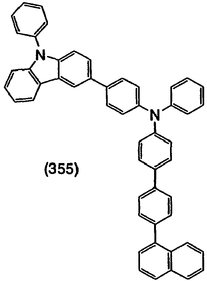
- A synthetic scheme of 4-(4-bromophenyl)-4'-phenyl-triphenylamine in
Step 1 is shown in the following (M-1).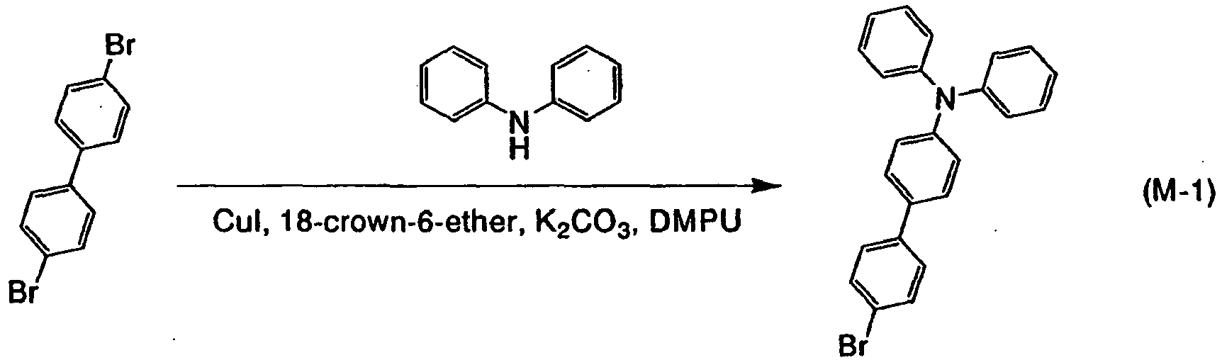
- In a 500-mL three-neck flask, 22 g (70 mmol) of 4,4'-dibromobiphenyl, 8.5 g (50 mmol) of diphenylamine, 1.9 g (10 mmol) of copper(I) iodide, 2.6 g (10 mmol) of 18-crown-6-ether, 6.9 g (50 mmol) of potassium carbonate, and 50 mL of 1,3-dimethyl-3,4,5,6-tetrahydro-2(1H)pyrimidinone (abbreviation: DMPU) were put, and the mixture was stirred under a nitrogen atmosphere at 180 °C for 37 hours.
- After the reaction, 500 mL of toluene was added to this reaction mixture, and this suspension was filtrated through Florisil, silica gel, and then Celite. The obtained filtrate was washed with water. Then, magnesium sulfate was added to remove moisture. This suspension was filtrated through Florisil, alumina, silica gel, and then Celite to obtain filtrate. The obtained filtrate was concentrated and purified by silica gel column chromatography (developing solvent, toluene: hexane = 1:4). The obtained fraction was concentrated, and hexane and methanol were added thereto. The mixture was irradiated with supersonic and then recrystallized to obtain 5.3 g of an objective white powder at a yield of 27 %.
- An Rf value of the objective substance by a silica gel thin layer chromatography (TLC) (developing solvent, ethyl acetate: hexane = 1:10) was 0.5 and that of 4,4'-dibromobiphenyl was 0.59.
- A synthetic scheme of [4'-(1-naphthyl)biphenyl-4-yl]diphenylamine in
Step 2 is shown in the following (M-2).
- In a 100-mL three-neck flask, 4.0 g (10 mmol) of 4-(4-bromophenyl)-4'-phenyl-triphenylamine, 1.7 g (10 mmol) of 1-naphthaleneboronic acid, 11 mg (0.05 mmol) of palladium(II) acetate, and 15 mg (0.05 mmol) of tri(o-tolyl)phosphine were put, and 20 mL of toluene, 5 mL of ethanol, and 10 mL of a potassium carbonate solution (2 mol/L) were added to this mixture. This mixture was deaerated while being stirred under low pressure. After the deaeration, the mixture was stirred under a nitrogen atmosphere at 90 °C for 7 hours to be reacted.
- After the reaction, 150 mL of toluene was added to this reaction mixture, and this suspension was filtrated through silica gel, alumina, and then Celite. The obtained filtrate was washed with water. Then, magnesium sulfate was added to remove moisture. This suspension was filtrated through silica gel, alumina, and then Celite to obtain filtrate. The obtained filtrate was concentrated, and methanol was added thereto. The mixture was irradiated with supersonic and then recrystallized to obtain 3.6 g of an objective white powder at a yield of 80 %.
- An Rf value of the objective substance by a silica gel thin layer chromatography (TLC) (developing solvent, ethyl acetate: hexane = 1:10) was 0.58 and that of 4-bromophenyl-4'-phenyl-triphenylamine was 0.65.
- A synthetic scheme of (4-bromophenyl)[4'-(1-naphthyl)biphenyl-4-yl]phenylamine in
Step 3 is shown in the following (M-3).
- After 3.6 g (8.0 mmol) of [4'-(1-naphthyl)biphenyl-4-yl]diphenylamine was dissolved in 100 mL of ethyl acetate in a 200-mL conical flask, 1.4 g (8.0 mmol) of N-bromo succinimide (abbreviation: NBS) was added to this solution. After that, this mixture was stirred at room temperature for 72 hours. After completion of the reaction, this mixture solution was washed with water, and magnesium sulfate was added thereto to remove moisture. This mixture solution was filtrated, the obtained filtrate was concentrated, and methanol was added thereto. The mixture was irradiated with supersonic and then recrystallized to obtain 3.9 g of an objective white powder at a yield of 93 %.
- A synthetic scheme of [4'-(1-naphthyl)biphenyl-4-yl](phenyl)[4-(9-phenyl-9H-carbazol-3-yl)phenyl]amine in
Step 4 is shown in the following (M-4).
- In a 100-mL three-neck flask, 1.6 g (3 mmol) of (4-bromophenyl)[4'-(1-naphthyl)biphenyl-4-yl]phenylamine, 0.8 g (3 mmol) of 9-phenyl-9H-carbazol-3-boronic acid, 6.0 mg (0.03 mmol) of palladium(II) acetate, and 18 mg (0.03 mmol) of tri(o-tolyl)phosphine were put, and 20 mL of toluene, 5 mL of ethanol, and 3 mL of a potassium carbonate solution (2 mol/L) were added to this mixture. This mixture was deaerated while being stirred under low pressure. After the deaeration, the mixture was stirred under a nitrogen atmosphere at 80 °C for 6.5 hours to be reacted.
- After the reaction, 150 mL of toluene was added to this reaction mixture, and this suspension was filtrated through Florisil, silica gel, and then Celite. The obtained filtrate was washed with water. Then, magnesium sulfate was added to remove moisture. This suspension was filtrated through Florisil, alumina, and then Celite to obtain filtrate. The obtained filtrate was concentrated and purified by silica gel column chromatography (developing solvent, toluene: hexane = 1:4). The obtained fraction was concentrated, and methanol was added thereto. The mixture was irradiated with supersonic and then recrystallized to obtain 1.2 g of an objective white powder at a yield of 60 %.
- An Rf value of the objective substance by a silica gel thin layer chromatography (TLC) (developing solvent, ethyl acetate: hexane = 1:10) was 0.28 and that of (4-bromophenyl)[4'-(1-naphthyl)biphenyl-4-yl]phenylamine was 0.42.
- A compound which was obtained through the
above Step 4 was measured by a nuclear magnetic resonance method (1H NMR). The measurement result is described below, and the 1H NMR chart is shown inFIGS. 50A and 50B . It was found from the measurement result that the carbazole derivative of the present invention, PCBANT (abbreviation) represented by the above structural formula (355), was obtained. 1H NMR (CDCl3, 300 MHz): δ (ppm) = 7.08 (t, J = 7.5 Hz, 1H), 7.20-7.73 (m, 30H), 7.87 (d, J = 8.1 Hz, 1H), 7.92 (d, J = 7.2 Hz, 1H), 8.00 (d, J = 8.4 Hz, 1H), 8.19 (d, J = 7.8 Hz, 1H), 8.35 (d, J = 1.8 Hz, 1H). - Molecular weight of the above compound was measured by a TOF-MS detector (Waters Micromass LCT Premier, manufactured by Waters). A mixture solution containing acetonitrile and 0.1 % of a formic acid solution (mixture rate of acetonitrile and the formic acid solution, 80/20 vol/vol) was used as a solvent. Accordingly, a main peak with a molecular weight of 689.30 (mode is ES+) was detected, and it was confirmed that an objective PCBANT (abbreviation) was obtained.
- In addition, an absorption spectrum of PCBANT (abbreviation) (measurement range: 200 nm to 800 nm) was measured. In the case of the toluene solution, an absorption peak on a long wavelength side was observed at around 342 nm, and in the case of the thin film, an absorption peak on a long wavelength side was observed at around 351 nm.
- In addition, an emission spectrum of PCBANT (abbreviation) (measurement range: 370 nm to 550 nm) was measured. In the case of the toluene solution, a maximum emission wavelength was 414 nm (excitation wavelength: 355 nm), and in the case of the thin film, a maximum emission wavelength was 342 nm (excitation wavelength: 365 nm). Since the measurement method of an absorption spectrum and an emission spectrum is similar to that of
Embodiment 1, the description is omitted. - The result of measuring the thin film using a photoelectron spectrometer (AC-2, manufactured by Riken Keiki Co., Ltd.) under the atmosphere indicated that the HOMO level of PCBANT (abbreviation) was -5.38 eV. The Tauc plot of the absorption spectrum of the thin film revealed that the absorption edge was 3.11 eV. Thus, the energy gap in the solid state was estimated to be 3.11 eV, which means that the LUMO level of PCBANT (abbreviation) is -2.27 eV.
- An oxidation-reduction reaction characteristic of PCBANT (abbreviation) was examined by a cyclic voltammetry (CV) measurement. Since the measurement method is similar to that of
Embodiment 1, the description is omitted. - According to the calculation similar to that of
Embodiment 1, the HOMO level of PCBANT (abbreviation) was found to be = -5.43 [eV]. In addition, the oxidation peak took a similar value even after the 100 cycles. Accordingly, it was found that repetition of the oxidation reduction between an oxidation state and a neutral state had favorable characteristics. - In addition, the glass transition temperature of PCBANT (abbreviation) was examined with a differential scanning calorimetry (
Pyris 1 DSC, manufactured by Perkin Elmer Co., Ltd.). According to the measurement results, it was found that the glass transition temperature was 131 °C. In this manner, PCBANT (abbreviation) has a high glass transition temperature and favorable heat resistance. In addition, the crystallization peak does not exist; thus, it was found that PCBANT (abbreviation) is a substance which is hard to be crystallized. - Note that the efficiency, the drive voltage at a luminance of about 1000 cd/m2, and the reliability of a light-emitting element formed using PCBANT (abbreviation) which was synthesized in Embodiment 11 in a manner similar to that of
Embodiment 5 for a hole-transporting layer, favorable values equivalent to those of the light-emittingelement 8 which was formed using PCBBiNB inEmbodiment 10 were obtained. When the drive voltage of the light-emitting element was 4.0 V, the luminance and the current value were 1186 cd/m2 and 0.73 mA, respectively, and the light-emitting element exhibited 65 % of the initial luminance when driven for 180 hours. - In
Embodiment 12, a synthetic method of a carbazole derivative of the present invention, 4-[9-(biphenyl-4-yl)-9H-carbazol-3-yl)-4'-phenyl-triphenylamine (abbreviation: BCBA1BP) represented by a structural formula (63), will be specifically described.
- A synthetic scheme of 9-(biphenyl-4-yl)-9H-carbazole in
Step 1 is shown in the following (N-1).
- In a 200-mL three-neck flask, 12 g (50 mmol) of 4-bromobiphenyl, 8.4 g (50 mmol) of carbazole, 230 mg (1 mmol) of palladium acetate (abbreviation: Pd(OAc)(II)), 1.8 g (3.0 mmol) of 1,1-bis(diphenylphosphino)ferrocene (abbreviation: DPPF), and 13 g (180 mmol) of sodium tert-butoxide were put, and the atmosphere of the flask was substituted by nitrogen. Then, 80 mL of dehydrated xylene was added to this mixture. This mixture was deaerated while being stirred under low pressure, and the mixture was stirred under a nitrogen atmosphere at 120 °C for 7.5 hours to be reacted.
- After completion of the reaction, about 600 mL of heated toluene was added to this suspension, and filtrated twice through Florisil, alumina, and then Celite. The obtained filtrate was concentrated, and hexane was added thereto. The mixture was recrystallized to obtain 14 g of an objective white powder at a yield of 87 %.
- A synthetic scheme of 9-(biphenyl-4-yl)-3-bromo-9H-carbazole in
Step 2 is shown in the following (N-2).
- After 3.1 g (10 mmol) of 9-(biphenyl-4-yl)-9H-carbazole was dissolved in 100 mL of chloroform in a 200-mL conical flask, 1.8 g (10 mmol) of N-bromo succinimide (abbreviation: NBS) was added to this solution. After that, this mixture was stirred at room temperature for 24 hours. After completion of the reaction, this mixture solution was washed with water, and magnesium sulfate was added thereto to remove moisture. This mixture solution was filtrated, and the obtained filtrate was concentrated and dried to obtain 3.7 g of an objective white powder at a yield of 95 %.
- A synthetic scheme of [9-(biphenyl-4-yl)-9H-carbazol-3-yl]boronic acid in
Step 3 is shown in the following (N-3).
- In a 500-mL three-neck flask, 8.0 g (20 mmol) of 9-(4-biphenyl)-3-bromo-9H-carbazole was put, and the atmosphere in the flask was substituted by nitrogen. Then, 200 mL of tetrahydrofuran (abbreviation: THF) was added thereto to reach -78 °C. After that, 16 mL (24 mmol) of an n-butyllithium hexane solution (1.6 mol/L) was dropped onto this mixture solution, and the solution was stirred for 2 hours. Then, 4.0 mL (40 mmol) of trimethyl borate was added to this reaction mixture, and the mixture was stirred at -78 °C for 2 hours and at room temperature for 18 hours. After the reaction, 50 mL of 1M dilute hydrochloric acid was added to this reaction solution, and the mixture was stirred for 3 hours. This mixture was extracted with toluene, and the obtained organic layer was washed with a saturated saline solution. After the washing, magnesium sulfate was added to the organic layer to remove moisture. This suspension was filtrated, the obtained filtrate was concentrated, and hexane was added thereto. The mixture was irradiated with supersonic and then recrystallized to obtain 6.6 g of an objective white powder at a yield of 91 %.
- A synthetic scheme of 4-[9-(biphenyl-4-yl)-9H-carbazol-3-yl)-4'-phenyl-triphenylamine in
Step 4 is shown in the following (N-4).
- In a 50-mL three-neck flask, 1.2 g (3.0 mmol) of 4-bromo-4'-phenyl-triphenylamine, 1.1 g (3.0 mmol) of [9-(biphenyl-4-yl)-9H-carbazol-3-yl]boronic acid, 6.0 mg (0.03 mmol) of palladium(II) acetate, and 18 mg (0.06 mmol) of tri(o-tolyl)phosphine were put, and 20 mL of toluene, 5 mL of ethanol, and 3 mL of a potassium carbonate solution (2 mol/L) were added to this mixture. This mixture was deaerated while being stirred under low pressure. After the deaeration, the mixture was stirred under a nitrogen atmosphere at 90 °C for 6.5 hours to be reacted.
- After the reaction, 150 mL of toluene was added to this reaction mixture, and this suspension was filtrated through Florisil and then Celite. The obtained filtrate was washed with water. Then, magnesium sulfate was added to remove moisture. This suspension was filtrated through Florisil, alumina, silica gel, and then Celite to obtain filtrate. The obtained filtrate was concentrated, and acetone and methanol were added thereto. The mixture was irradiated with supersonic and then recrystallized to obtain 1.5 g of an objective white powder at a yield of 79 %.
- An Rf value of the objective substance by a silica gel thin layer chromatography (TLC) (developing solvent, ethyl acetate: hexane = 1:10) was 0.45 and that of 4-bromo-4'-phenyl-triphenylamine was 0.68.
- A compound which was obtained through the
above Step 4 was measured by a nuclear magnetic resonance method (1H NMR). The measurement result is described below, and the 1H NMR chart is shown inFIGS. 51A and 51B . It was found from the measurement result that the carbazole derivative of the present invention, BCBA1BP (abbreviation) represented by the above structural formula (63), was obtained. 1H NMR (CDCl3, 300 MHz): δ (ppm) = 7.06 (t, J = 7.2 Hz, 1H), 7.20-7.72 (m, 29H), 7.83 (d, J = 8.4 Hz, 2H), 8.19 (d, J = 7.8 Hz, 1H), 8.35 (s, 1H). - Molecular weight of the above compound was measured by a TOF-MS detector (Waters Micromass LCT Premier, manufactured by Waters). A mixture solution containing acetonitrile and 0.1 % of a formic acid solution (mixture rate of acetonitrile and the formic acid solution, 80/20 vol/vol) was used as a solvent. Accordingly, a main peak with a molecular weight of 638.27 (mode is ES+) was detected, and it was confirmed that an objective BCBA1BP (abbreviation) was obtained.
- In addition, an absorption spectrum of PCBA1BP (abbreviation) (measurement range: 200 nm to 800 nm) was measured. In the case of the toluene solution, an absorption peak on a long wavelength side was observed at around 336 nm, and in the case of the thin film, an absorption peak on a long wavelength side was observed at around 342 nm.
- In addition, an emission spectrum of PCBA1BP (abbreviation) (measurement range: 370 nm to 550 nm) was measured. In the case of the toluene solution, a maximum emission wavelength was 394 nm (excitation wavelength: 350 nm), and in the case of the thin film, a maximum emission wavelength was 408 nm (excitation wavelength: 301 nm). Since the measurement method of an absorption spectrum and an emission spectrum is similar to that of
Embodiment 1, the description is omitted. - The result of measuring the thin film using a photoelectron spectrometer (AC-2, manufactured by Riken Keiki Co., Ltd.) under the atmosphere indicated that the HOMO level of PCBA1BP (abbreviation) was -5.48 eV. The Tauc plot of the absorption spectrum of the thin film revealed that the absorption edge was 3.19 eV. Thus, the energy gap in the solid state was estimated to be 3.19 eV, which means that the LUMO level of PCBA1BP (abbreviation) is -2.29 eV.
- An oxidation-reduction reaction characteristic of PCBA1BP (abbreviation) was examined by a cyclic voltammetry (CV) measurement. Since the measurement method is similar to that of
Embodiment 1, the description is omitted. - According to the calculation similar to that of
Embodiment 1, the HOMO level of PCBA1BP (abbreviation) was found to be = -5.43 [eV]. In addition, the oxidation peak took a similar value even after the 100 cycles. Accordingly, it was found that repetition of the oxidation reduction between an oxidation state and a neutral state had favorable characteristics. - In addition, the glass transition temperature of PCBA1BP (abbreviation) was examined with a differential scanning calorimetry (
Pyris 1 DSC, manufactured by Perkin Elmer Co., Ltd.). According to the measurement results, it was found that the glass transition temperature was 122 °C. In this manner, PCBA1BP (abbreviation) has a high glass transition temperature and favorable heat resistance. In addition, the crystallization peak does not exist; thus, it was found that PCBA1BP (abbreviation) is a substance which is hard to be crystallized. - Note that the efficiency, the drive voltage at a luminance of about 1000 cd/m2, and the reliability of a light-emitting element formed using PCBA1BP (abbreviation) which was synthesized in
Embodiment 12 in a manner similar to that ofEmbodiment 5 for a hole-transporting layer, favorable values equivalent to those of the light-emittingelement 8 which was formed using PCBBiNB inEmbodiment 10 were obtained. When the drive voltage of the light-emitting element was 4.0 V, the luminance and the current value were 1031 cd/m2 and 0.72 mA, respectively, and the light-emitting element exhibited 89 % of the initial luminance when driven for 180 hours. - In Embodiment 13, a synthetic method of a carbazole derivative of the present invention, 4-[9-(biphenyl-4-yl)-9H-carbazol-3-yl)-4'-(1-naphthyl)triphenylamine (abbreviation: BCBANB) represented by a structural formula (364), will be specifically described.

- A synthetic scheme of 4-bromotriphenylamine in
Step 1 is shown in the following (O-1).
- To 1.5 L of an ethyl acetate solution containing 54.0 g (220 mmol) of triphenylamine, 35.6 g (200 mmol) of N-bromo succinimide (abbreviation: NBS) was added. Then, the mixture was stirred for 24 hours. After the obtained suspension was concentrated to 1 L, the concentrated suspension was washed with 1 L of an aqueous solution containing 5 % of sodium acetate. After the washing, this solution was further concentrated to about 50 mL. Then, methanol was added to the concentrated solution and the solution was precipitated. The obtained precipitate was filtered and dried to obtain 46.5 g of an objective white powder at a yield of 73 %.
- A synthetic scheme of 4-(1-naphthyl)triphenylamine in
Step 2 is shown in the following (O-2).
- In a 20mL three-neck flask, 9.7 g (30 mmol) of 4-bromotriphenylamine, 5.7 g (33 mmol) of 1-naphthaleneboronic acid, 67 mg (0.3 mmol) of palladium(II) acetate, and 91 g (0.3 mmol) of tri(o-tolyl)phosphine were put, and 20 mL of toluene, 20 mL of ethanol, and 20mL of a potassium carbonate solution (2 mol/L) were added to this mixture. This mixture was deaerated while being stirred under low pressure. After the deaeration, the mixture was stirred under a nitrogen atmosphere at 90 °C for 2 hours to be reacted.
- After the reaction, 150 mL of toluene was added to this reaction mixture, and this suspension was filtrated through Florisil, silica gel, and then Celite. The obtained filtrate was washed with sodium hydrogen carbonate solution and water in this order, and magnesium sulfate was added thereto to dry the filtrate. After the drying, this suspension was filtrated through Florisil, alumina, silica gel, and then Celite to obtain filtrate. The obtained filtrate was concentrated and dried to obtain 11 g of an objective light-yellow solid at a yield of 99 %.
- An Rf value of the objective substance by a silica gel thin layer chromatography (TLC) (developing solvent, ethyl acetate: hexane = 1:10) was 0.48 and that of 4-bromotriphenylamine was 0.55.
- A compound which was obtained through the
above Step 2 was measured by a nuclear magnetic resonance method (1H NMR). It was found from the measurement result that the compound of the present invention represented by the above structural formula (364) was obtained. 1H NMR (CDCl3, 300 MHz): δ (ppm) = 7.07 (t, J = 7.5 Hz, 1H), 7.22-7.61 (m, 21H), 7.83 (d, J = 7.8 Hz, 1H), 7.88-7.91 (m, 1H), 8.02-8.05 (m, 1H). - A synthetic scheme of 4-bromo-4'-(1-naphthyl)triphenylamine in
Step 3 is shown in the following (O-3).
- After 11 g (30 mmol) of 4-(1-naphthyl)triphenylamine was dissolved in 300 mL of ethyl acetate in a 500-mL recovery flask, 5.3 g (30 mmol) of N-bromo succinimide (abbreviation: NBS) was added to this solution. After that, this mixture was stirred at room temperature for 168 hours. After completion of the reaction, this mixture solution was washed with water, and magnesium sulfate was added thereto to remove moisture. This mixture solution was filtrated, and the obtained filtrate was concentrated and purified by silica gel column chromatography (developing solvent, toluene: hexane = 1:4). The obtained fraction was concentrated, and methanol was added thereto. The mixture was irradiated with supersonic and then recrystallized to obtain 7.8 g of an objective white powder at a yield of 43 %.
- A synthetic scheme of 4-[9-(biphenyl-4-yl)-9H-carabazol-3-yl]-4'-(1-naphthyl)triphenylamine in
Step 4 is shown in the following (O-4).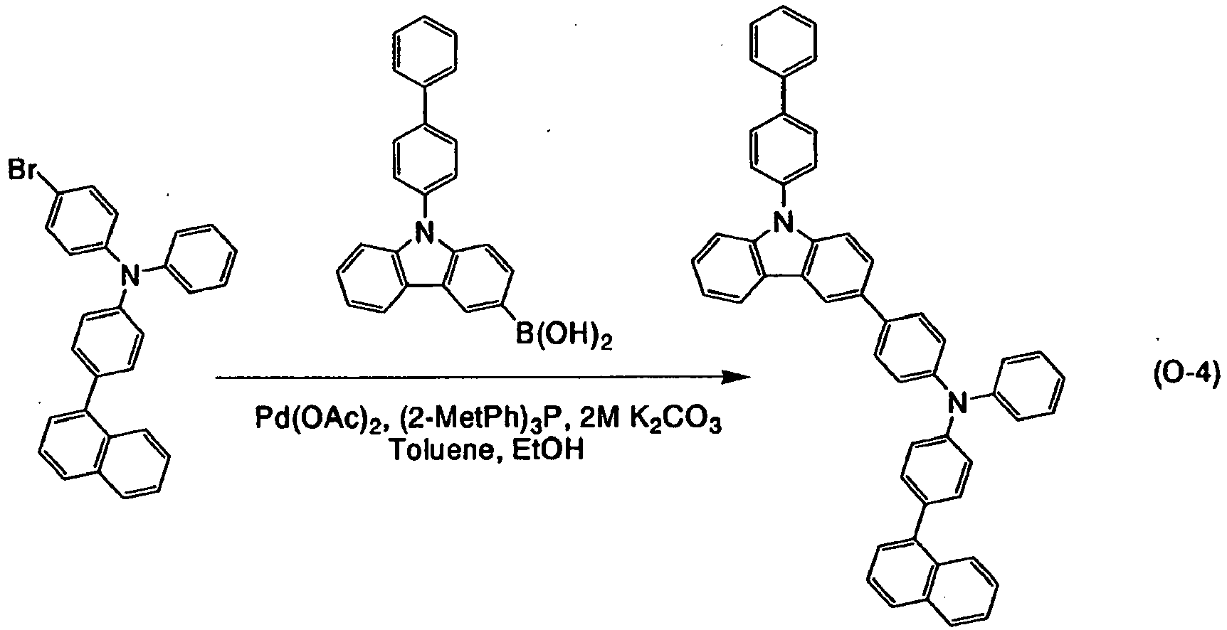
- In a 100-mL three-neck flask, 1.35 g (3.0 mmol) of 4-bromo-4'-(1-naphthyl)triphenylamine, 1.1 g (3.0 mmol) of [9-(biphenyl-4-yl)-9H-carbazol-3-yl]boronic acid, 6.0 mg (0.02 mmol) of palladium(II) acetate, and 9.0 mg (0.06 mmol) of tri(o-tolyl)phosphine were put, and 20 mL of toluene, 5 mL of ethanol, and 3 mL of a potassium carbonate solution (2 mol/L) were added to this mixture. This mixture was deaerated while being stirred under low pressure. After the deaeration, the mixture was stirred under a nitrogen atmosphere at 90 °C for 3 hours to be reacted.
- After the reaction, 150 mL of toluene was added to this reaction mixture, and this suspension was filtrated through Florisil, silica gel, and then Celite. The obtained filtrate was washed with water. Then, magnesium sulfate was added to remove moisture. This suspension was filtrated through Florisil, alumina, silica gel, and then Celite to obtain filtrate. The obtained filtrate was concentrated and purified by silica gel column chromatography (developing solvent, toluene: hexane = 1:4). The obtained fraction was concentrated, and acetone and methanol were added thereto. The mixture was irradiated with supersonic and then recrystallized to obtain 1.0 g of an objective white powder at a yield of 50 %.
- An Rf value of the objective substance by a silica gel thin layer chromatography (TLC) (developing solvent, ethyl acetate: hexane = 1:10) was 0.45 and that of 4-bromo-4'-(1-naphthyl)triphenylamine was 0.66.
- A compound which was obtained through the
above Step 4 was measured by a nuclear magnetic resonance method (1H NMR). The measurement result is described below, and the 1H NMR chart is shown inFIGS. 52A and 52B . It was found from the measurement result that the carbazole derivative of the present invention, BCBANB (abbreviation) represented by the above structural formula (364), was obtained. 1H NMR (CDCl3, 300 MHz): δ (ppm) = 7.08 (t, J = 6.9 Hz, 1H), 7.28-7.71 (m, 28H), 7.82-7.86 (m, 3H), 7.89-7.92 (m, 1H), 8.04-8.07 (m, 1H), 8.20 (d, J = 7.8 Hz, 1H), 8.37 (d, J = 1.2 Hz, 1H). - Molecular weight of the above compound was measured by a TOF-MS detector (Waters Micromass LCT Premier, manufactured by Waters). A mixture solution containing acetonitrile and 0.1 % of a formic acid solution (mixture rate of acetonitrile and the forminc acid solution, 80/20 vol/vol) was used as a solvent. Accordingly, a main peak with a molecular weight of 556.52 (mode is ES+) was detected, and it was confirmed that an objective BCBANB (abbreviation) was obtained.
- In addition, an absorption spectrum of BCBANB (abbreviation) (measurement range: 200 nm to 800 nm) was measured. In the case of the toluene solution, an absorption peak on a long wavelength side was observed at around 335 nm, and in the case of the thin film, an absorption peak on a long wavelength side was observed at around 344 nm.
- In addition, an emission spectrum of BCBANB (abbreviation) (measurement range: 370 nm to 550 nm) was measured. In the case of the toluene solution, a maximum emission wavelength was 410 nm (excitation wavelength: 345 nm), and in the case of the thin film, a maximum emission wavelength was 422 nm (excitation wavelength: 328 nm).
- Since the measurement method of an absorption spectrum and an emission spectrum is similar to that of
Embodiment 1, the description is omitted. - The result of measuring the thin film using a photoelectron spectrometer (AC-2, manufactured by Riken Keiki Co., Ltd.) under the atmosphere indicated that the HOMO level of BCBANB (abbreviation) was -5.42 eV. The Tauc plot of the absorption spectrum of the thin film revealed that the absorption edge was 3.19 eV. Thus, the energy gap in the solid state was estimated to be 3.19 eV, which means that the LUMO level of BCBANB (abbreviation) is -2.23 eV.
- An oxidation-reduction reaction characteristic of BCBANB (abbreviation) was examined by a cyclic voltammetry (CV) measurement. Since the measurement method is similar to that of
Embodiment 1, the description is omitted. - According to the calculation similar to that of
Embodiment 1, the HOMO level of BCBANB (abbreviation) was found to be = -5.45 [eV]. In addition, the oxidation peak took a similar value even after the 100 cycles. Accordingly, it was found that repetition of the oxidation reduction between an oxidation state and a neutral state had favorable characteristics. - In addition, the glass transition temperature of BCBANB (abbreviation) was examined with a differential scanning calorimetry (
Pyris 1 DSC, manufactured by Perkin Elmer Co., Ltd.). According to the measurement results, it was found that the glass transition temperature was 130 °C. In this manner, BCBANB (abbreviation) has a high glass transition temperature and favorable heat resistance. In addition, the crystallization peak does not exist; thus, it was found that BCBANB (abbreviation) is a substance which is hard to be crystallized. - Note that the efficiency, the drive voltage at a luminance of about 1000 cd/m2, and the reliability of a light-emitting element formed using BCBANB (abbreviation) which was synthesized in Embodiment 13 in a manner similar to that of
Embodiment 5 for a hole-transporting layer, favorable values equivalent to those of the light-emittingelement 8 which was formed using PCBBiNB inEmbodiment 10 were obtained. When the drive voltage of the light-emitting element was 4.0 V, the luminance and the current value were 848 cd/m2 and 0.52 mA, respectively. - In Embodiment 14, a synthetic method of a carbazole derivative of the present invention,
4-[9-(biphenyl-4-yl)-9H-carbazol-3-yl)-4'-(1-naphthyl)4"-phenyl-triphenylamine (abbreviation: BCBBiNB) represented by a structural formula (366), will be specifically described.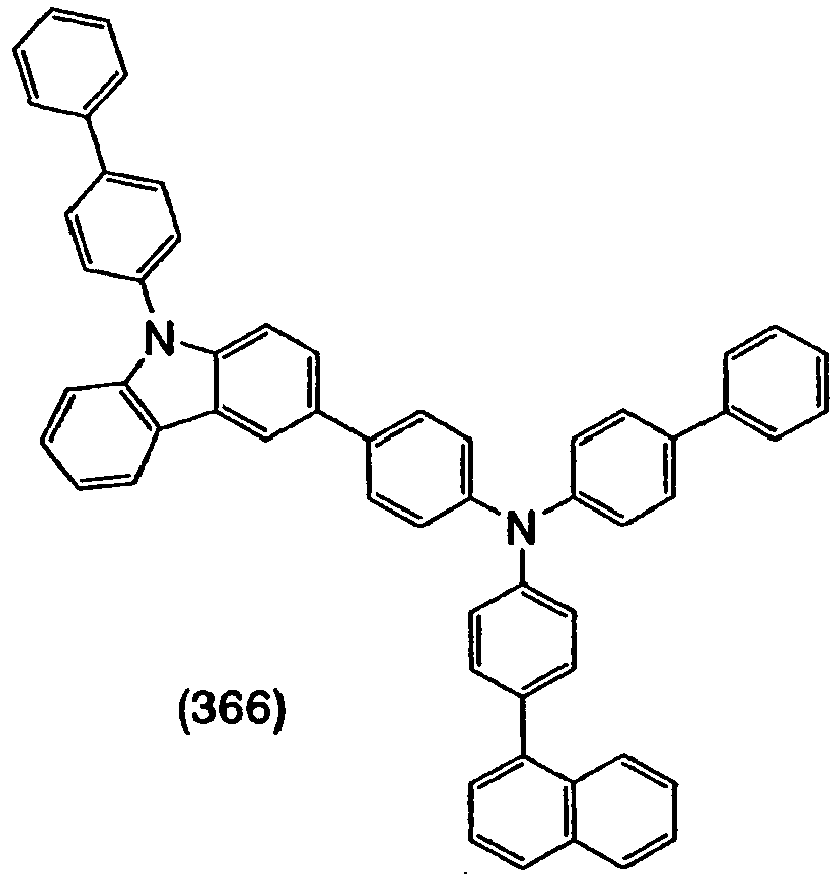
- A synthetic scheme of 4-[9-(biphenyl-4-yl)-9H-carbazol-3-yl)-4'-(1-naphthyl)4"-phenyl-triphenylamine in
Step 1 is shown in the following (P-1).
- In a 100-mL three-neck flask, 1.6 g (3.0 mmol) of 4-bromo-4'-(1-naphthyl)-4"-phenyl-triphenylamine, 1.1 g (3.0 mmol) of [9-(biphenyl-4-yl)-9H-carbazol-3-yl]boronic acid, 6.0 mg (0.03 mmol) of palladium(II) acetate, and 18 mg (0.03 mmol) of tri(o-tolyl)phosphine were put, and 20 mL of toluene, 5 mL of ethanol, and 3 mL of a potassium carbonate solution (2 mol/L) were added to this mixture. This mixture was deaerated while being stirred under low pressure. After the deaeration, the mixture was stirred under a nitrogen atmosphere at 90 °C for 6.5 hours to be reacted.
- After the reaction, 150 mL of toluene was added to this reaction mixture, and this suspension was filtrated through Florisil, silica gel, and then Celite. The obtained filtrate was washed with water. Then, magnesium sulfate was added to remove moisture. This suspension was filtrated through Florisil, alumina, silica gel, and then Celite to obtain filtrate. The obtained filtrate was concentrated and purified by silica gel column chromatography (developing solvent, toluene: hexane = 1:4). The obtained fraction was concentrated, and acetone and methanol were added thereto. The mixture was irradiated with supersonic and then recrystallized to obtain 1.4 g of an objective white powder at a yield of 60 %.
- An Rf value of the objective substance by a silica gel thin layer chromatography (TLC) (developing solvent, ethyl acetate: hexane = 1:10) was 0.26 and that of 4-bromo-4'-(1-naphthyl)-4"-phenyl-triphenylamine was 0.46.
- A compound which was obtained through the
above Step 1 was measured by a nuclear magnetic resonance method (1H NMR). The measurement result is described below, and the 1H NMR chart is shown inFIGS. 53A and 53B . It was found from the measurement result that the carbazole derivative of the present invention, BCBBiNB (abbreviation) represented by the above structural formula (366), was obtained. 1H NMR (CDCl3, 300 MHz): δ (ppm) = 7.30-7.71 (m, 33H), 7.82-7.86 (m, 3H), 7.90-7.93 (m, 1H), 8.05-8.08 (m, 1H), 8.20 (d, J = 7.8 Hz, 1H), 8.38 (d, J = 1.5 Hz, 1H). - Molecular weight of the above compound was measured by a TOF-MS detector (Waters Micromass LCT Premier, manufactured by Waters). A mixture solution containing acetonitrile and 0.1 % of a formic acid solution (mixture rate of acetonitrile and the forminc acid solution, 80/20 vol/vol) was used as a solvent. Accordingly, a main peak with a molecular weight of 765.32 (mode is ES+) was detected, and it was confirmed that an objective BCBBiNB (abbreviation) was obtained.
- In addition, an absorption spectrum of BCBBiNB (abbreviation) (measurement range: 200 nm to 800 nm) was measured. In the case of the toluene solution, an absorption peak on a long wavelength side was observed at around 342 nm, and in the case of the thin film, an absorption peak on a long wavelength side was observed at around 351 nm.
- In addition, an emission spectrum of BCBBiNB (abbreviation) (measurement range: 370 nm to 550 nm) was measured. In the case of the toluene solution, a maximum emission wavelength was 409 nm (excitation wavelength: 355 nm), and in the case of the thin film, a maximum emission wavelength was 433 nm (excitation wavelength: 336 nm).
- Since the measurement method of an absorption spectrum and an emission spectrum is similar to that of
Embodiment 1, the description is omitted. - The result of measuring the thin film using a photoelectron spectrometer (AC-2, manufactured by Riken Keiki Co., Ltd.) under the atmosphere indicated that the HOMO level of BCBBiNB (abbreviation) was -5.35 eV. The Tauc plot of the absorption spectrum of the thin film revealed that the absorption edge was 3.18 eV. Thus, the energy gap in the solid state was estimated to be 3.18 eV, which means that the LUMO level of BCBBiNB (abbreviation) is -2.17 eV.
- An oxidation-reduction reaction characteristic of BCBBiNB (abbreviation) was examined by a cyclic voltammetry (CV) measurement. Since the measurement method is similar to that of
Embodiment 1, the description is omitted. - According to the calculation similar to that of
Embodiment 1, the HOMO level of BCBBiNB (abbreviation) was found to be = -5.42 [eV]. In addition, the oxidation peak took a similar value even after the 100 cycles. Accordingly, it was found that repetition of the oxidation reduction between an oxidation state and a neutral state had favorable characteristics. - In addition, the glass transition temperature of BCBBiNB (abbreviation) was examined with a differential scanning calorimetry (
Pyris 1 DSC, manufactured by Perkin Elmer Co., Ltd.). According to the measurement results, it was found that the glass transition temperature was 143 °C. In this manner, BCBBiNB (abbreviation) has a high glass transition temperature and favorable heat resistance. In addition, the crystallization peak does not exist; thus, it was found that BCBBiNB (abbreviation) is a substance which is hard to be crystallized. - Note that the efficiency, the drive voltage at a luminance of about 1000 cd/m2, and the reliability of a light-emitting element formed using BCBBiNB (abbreviation) which was synthesized in Embodiment 14 in a manner similar to that of
Embodiment 5 for a hole-transporting layer, favorable values equivalent to those of the light-emittingelement 8 which was formed using PCBBiNB inEmbodiment 10 were obtained. When the drive voltage of the light-emitting element was 4.0 V, the luminance and the current value were 996 cd/m2 and 0.59 mA, respectively, and the light-emitting element exhibited 84 % of the initial luminance when driven for 180 hours. - In Embodiment 15, a synthetic method of a carbazole derivative of the present invention, 4-{9-[4-(1-naphthyl)phenyl]-9H-carbazol-3-yl}-4'-phenyl-triphenylamine (abbreviation: NBCBA1BP) represented by a structural formula (386), will be specifically described.

- A synthetic scheme of 9-(4-bromophenyl)-9H-carbazole in
Step 1 is shown in the following (Q-1).
- In a 300-mL three-neck flask, 56 g (240 mmol) of 1,4-dibromobenzene, 31 g (180 mmol) of 9H-carabazole, 4.6 g (24 mmol) of copper(I) iodide, 2.1 g (8.0 mmol) of 18-crown-6-ether, 66 g (480 mmol) of potassium carbonate, and 8 mL of 1,3-dimethyl-3,4,5,6-tetrahydro-2(1H)pyrimidinone (abbreviation: DMPU) were put, and the mixture was stirred under a nitrogen atmosphere at 180 °C for 6 hours.
- After the reaction, this suspension was filtrated, and the filtrate was washed with dilute hydrochloric acid, a saturated sodium hydrogen carbonate solution, and a saturated saline solution in this order. Then, moisture was removed by magnesium sulfate. This suspension was filtrated, and the obtained filtrate was concentrated and purified by silica gel column chromatography (developing solvent, toluene: hexane = 9:1). The obtained fraction was concentrated, and chloroform and hexane were added thereto. The mixture was irradiated with supersonic and then recrystallized to obtain 21 g of an objective light brown plate-like crystal at a yield of 35 %.
- A synthetic scheme of 9-[4-(1-naphthyl)phenyl]-9H-carbazole in
Step 2 is shown in the following (Q-2).
- In a 100-mL three-neck flask, 4.8 g (15 mmol) of 9-(4-bromophenyl)-9H-carbazole, 2.6 g (15 mmol) of 1-naphthaleneboronic acid, 2.0 mg (0.01 mmol) of palladium(II) acetate, and 6.0 mg (0.02 mmol) of tri(o-tolyl)phosphine were put, and 20 mL of toluene, 10 mL of ethanol, and 10 mL of a potassium carbonate solution (2 mol/L) were added to this mixture. This mixture was deaerated while being stirred under low pressure. After the deaeration, the mixture was stirred under a nitrogen atmosphere at 90 °C for 9 hours to be reacted.
- After the reaction, 150 mL of toluene was added to this reaction mixture, and this suspension was filtrated through Florisil and then Celite. The obtained filtrate was washed with water. Then, magnesium sulfate was added to remove moisture. This suspension was filtrated through Florisil, alumina, silica gel, and then Celite to obtain filtrate. The obtained filtrate was concentrated, and acetone and methanol were added thereto. The mixture was irradiated with supersonic and then recrystallized to obtain , 5.0 g of an objective white powder at a yield of 90 %.
- An Rf value of the objective substance by a silica gel thin layer chromatography (TLC) (developing solvent, ethyl acetate: hexane = 1:10) was 0.46 and that of 9-(4-bromophenyl)-9H-carbazole was 0.54.
- A synthetic scheme of 3-bromo-9-[4-(1-naphthyl)phenyl]-9H-carbazole in
Step 3 is shown in the following (Q-3).
- After 5.0 g (14 mmol) of 9-[4-(1-naphthyl)phenyl]-9H-carbazole was dissolved in a mixture solvent of 50 mL of toluene and 250 mL of ethyl acetate in a 300-mL conical flask, 2.5 g (14 mmol) of N-bromo succinimide (abbreviation: NBS) was added to this solution. After that, this mixture was stirred at room temperature for 168 hours. After completion of the reaction, this mixture solution was filtrated through Florisil and then Celite. Then, the obtained filtrate was washed with water, and magnesium sulfate was added thereto to remove moisture. This mixture solution was filtrated, the obtained filtrate was concentrated, and hexane was added thereto. Then, the mixture was irradiated with supersonic to obtain 6.1 g of an objective white powder at a yield of 99%.
- A synthetic scheme of 9-[4-(1-naphthyl)phenyl]-9H-carbazol-3-boronic acid in
Step 4 is shown in the following (Q-4).
- In a 500-mL three-neck flask, 5.0 g (14 mmol) of 3-bromo-9-[4-(1-naphthyl)phenyl]-9H-carbazole was put, and the atmosphere in the flask was substituted by nitrogen. Then, 200 mL of tetrahydrofuran (abbreviation: THF) was added thereto to reach -78 °C. 11 mL (17 mmol) of an n-butyllithium hexane solution (1.6 mol/L) was dropped onto this mixture solution, and the solution was stirred for 4 hours. After that, 2.7 mL (27 mmol) of trimethyl borate was added to this reaction mixture, and the mixture was stirred at -78 °C for 2 hours and at room temperature for 16 hours. After the reaction, 50 mL of 1M dilute hydrochloric acid was added to this reaction solution, and the mixture was stirred for 4 hours. This mixture was extracted with toluene, and the obtained organic layer was washed with a saturated saline solution. After the washing, magnesium sulfate was added to the organic layer to remove moisture. This suspension was filtrated, the obtained filtrate was concentrated, and chloroform and hexane were added thereto. The mixture was irradiated with supersonic and then recrystallized to obtain 3.5 g of an objective white powder at a yield of 63 %.
- A synthetic scheme of 4-{9-[4(1-naphthyl)phenyl)-9H-carbazol-3-yl}-4'-phenyl-triphenylamine in
Step 5 is shown in the following (Q-5).
- In a 50-mL three-neck flask, 1.0 g (2.5 mmol) of 4-bromo-4'-phenyl-triphenylamine, 1.0 g (2.5 mmol) of 9-[4-(1-naphthyl)phenyl]-9H-carbazol-3-boronic acid, 4.0 mg (0.02 mmol) of palladium(II) acetate, and 6.0 mg (0.02 mmol) of tri(o-tolyl)phosphine were put, and 20 mL of toluene, 5 mL of ethanol, and 2.5 mL of a potassium carbonate solution (2 mol/L) were added to this mixture. This mixture was deaerated while being stirred under low pressure. After the deaeration, the mixture was stirred under a nitrogen atmosphere at 90 °C for 13 hours to be reacted.
- After the reaction, 150 mL of toluene was added to this reaction mixture, and this suspension was filtrated through Florisil, silica gel, and then Celite. The obtained filtrate was washed with water. Then, magnesium sulfate was added to remove moisture. This suspension was filtrated through Florisil, alumina, silica gel, and then Celite to obtain filtrate. The obtained filtrate was concentrated, and acetone and methanol were added thereto. The mixture was irradiated with supersonic and then recrystallized to obtain 1.2 g of an objective white powder at a yield of 70 %.
- An Rf value of the objective substance by a silica gel thin layer chromatography (TLC) (developing solvent, ethyl acetate: hexane = 1:10) was 0.41 and that of 4-bromo-4'-phenyl-triphenylamine was 0.62.
- A compound which was obtained through the
above Step 5 was measured by a nuclear magnetic resonance method (1H NMR). The measurement result is described below, and the 1H NMR chart is shown inFIGS. 54A and 54B . It was found from the measurement result that the carbazole derivative of the present invention, NBCBA1BP (abbreviation) represented by the above structural formula (386), was obtained. 1H NMR (CDCl3, 300 MHz): δ (ppm) = 7.06 (t, J = 6.6 Hz, 1H), 7.21-7.77 (m, 30H), 7.92-7.98 (m, 2H), 8.04-8.08 (m, 1H), 8.22 (d, J = 7.8 Hz, 1H), 8.37 (d, J = 1.5 Hz, 1H). - In addition, an absorption spectrum of NBCBA1BP (abbreviation) (measurement range: 200 nm to 800 nm) was measured. In the case of the toluene solution, an absorption peak on a long wavelength side was observed at around 333 nm, and in the case of the thin film, an absorption peak on a long wavelength side was observed at around 340 nm.
- In addition, an emission spectrum of NBCBA1BP (abbreviation) (measurement range: 370 nm to 550 nm) was measured. In the case of the toluene solution, a maximum emission wavelength was 393 nm (excitation wavelength: 350 nm), and in the case of the thin film, a maximum emission wavelength was 488 nm (excitation wavelength: 302 nm).
- Since the measurement method of an absorption spectrum and an emission spectrum is similar to that of
Embodiment 1, the description is omitted. - The result of measuring the thin film using a photoelectron spectrometer (AC-2, manufactured by Riken Keiki Co., Ltd.) under the atmosphere indicated that the HOMO level of NBCBA1BP (abbreviation) was -5.53 eV The Tauc plot of the absorption spectrum of the thin film revealed that the absorption edge was 3.22 eV Thus, the energy gap in the solid state was estimated to be 3.22 eV, which means that the LUMO level of NBCBA1BP (abbreviation) is -2.31 eV.
- An oxidation-reduction reaction characteristic of NBCBA1BP (abbreviation) was examined by a cyclic voltammetry (CV) measurement. Since the measurement method is similar to that of
Embodiment 1, the description is omitted. - According to the calculation similar to that of
Embodiment 1, the HOMO level of NBCBA1BP (abbreviation) was found to be = -5.43 [eV]. In addition, the oxidation peak took a similar value even after the 100 cycles. Accordingly, it was found that repetition of the oxidation reduction between an oxidation state and a neutral state had favorable characteristics. - In addition, the glass transition temperature of NBCBA1BP (abbreviation) was examined with a differential scanning calorimetry (
Pyris 1 DSC, manufactured by Perkin Elmer Co., Ltd.). According to the measurement results, it was found that the glass transition temperature was 132 °C. In this manner, NBCBA1BP (abbreviation) has a high glass transition temperature and favorable heat resistance. In addition, the crystallization peak does not exist; thus, it was found that NBCBA1BP (abbreviation) is a substance which is hard to be crystallized. - Note that the efficiency, the drive voltage at a luminance of about 1000 cd/m2, and the reliability of a light-emitting element formed using NBCBA1BP (abbreviation) which was synthesized in Embodiment 15 in a manner similar to that of
Embodiment 5 for a hole-transporting layer, favorable values equivalent to those of the light-emittingelement 8 which was formed using PCBBiNB inEmbodiment 10 were obtained. When the drive voltage of the light-emitting element was 3.6 V, the luminance and the current value were 773 cd/m2 and 0.47 mA, respectively. - In
Embodiment 16, a synthetic method of a carbazole derivative of the present invention, 4-[9-(1-naphthyl)-9H-carbazol-3-yl]-4'-phenyl-triphenylamine (abbreviation: NCBA1BP) represented by a structural formula (395), will be specifically described.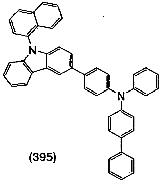
- A synthetic scheme of 9-(1-naphthyl)-9H-carbazole in
Step 1 is shown in the following (R-1).
- In a 500-mL three-neck flask, 21 g (100 mmol) of 1-bromonaphthalene, 17 g (100 mmol) of carabazole, 0.1 g (5.0 mmol) of copper(I) iodide, 0.7 g (2.5 mmol) of 18-crown-6-ether, 33 g (240 mmol) of potassium carbonate, and 80 mL of 1,3-dimethyl-3,4,5,6-tetrahydro-2(1H)-pyrimidinone (abbreviation: DMPU) were put, and the mixture was stirred under a nitrogen atmosphere at 170 °C for 6 hours. Then, 10 g (50 mmol) of 1-bromonaphthalene, 2.0 g (10 mmol) of copper(I) iodide, and 2.6 g (10 mmol) of 18-crown-6-ether were further added to this reaction mixture, and the mixture was further stirred at 170 °C for 7.5 hours. After that, 10 g (50 mmol) of 1-bromonaphthalene was further added to this reaction mixture, and the mixture was further stirred at 180 °C for 6 hours.
- After the reaction, about 200 mL of toluene and about 100 mL of hydrochloric acid (1 mol/L) were added to this reaction mixture, and the mixture was filtered through Celite. The obtained filtrate was filtrated through Florisil and Celite. The obtained filtrate was separated into an organic layer and an aqueous layer. After this organic layer was washed with hydrochloric acid (1 mol/L) and water in this order, magnesium sulfate was added to remove moisture. This suspension was filtered through Florisil and Celite. Then, hexane was added to the oily substance obtained by concentrating the obtained filtrate, and the mixture was irradiated with supersonic and then recrystallized to obtain 22 g of an objective white powder at a yield of 75 %.
- An Rf value of the objective substance by a silica gel thin layer chromatography (TLC) (developing solvent, ethyl acetate: hexane = 1:10) was 0.61, that of 1-bromonaphthalene was 0.74, and that of carbazole was 0.24.
- A synthetic scheme of 3-bromo-9-(1-naphthyl)-9H-carbazole in
Step 2 is shown in the following (R-2).
- After 5.9 g (20 mmol) of 9-(1-naphthyl)-9H-carbazole was dissolved in a mixture solvent of 50 mL of toluene and 50 mL of ethyl acetate in a 500-mL conical flask, 3.6 g (20 mmol) of N-bromo succinimide (abbreviation: NBS) was added to this solution. After that, this mixture was stirred at room temperature for 170 hours. After completion of the reaction, this mixture solution was washed with water, and magnesium sulfate was added thereto to remove moisture. This mixture solution was filtrated, and the obtained filtrate was concentrated and dried to obtain 7.4 g of an objective white powder at a yield of 99 %.
- An Rf value of the objective substance by a silica gel thin layer chromatography (TLC) (developing solvent, ethyl acetate: hexane = 1:10) was 0.43 and that of 9-(1-naphthyl)9H-carbazole was 0.35.
- A synthetic scheme of 9-(1-naphthyl)9H-carbazol-3-boronic acid in
Step 3 is shown in the following (R-3).
- In a 500-mL three-neck flask, 3.7 g (10 mmol) of 9-(1-naphthyl)9H-carbazole was put, and the atmosphere in the flask was substituted by nitrogen. Then, 200 mLof tetrahydrofuran (abbreviation: THF) was added thereto, and the mixture was stirred at -78°C. Then, 7 mL (13 mmol) of an n-butyllithium hexane solution (1.6 mol/L) was dropped onto this mixture solution, and the solution was stirred for 2 hours. After that, 2 mL (20 mmol) of trimethyl borate was added to this reaction mixture, and the mixture was stirred at -78 °C for 3 hours and at room temperature for 16 hours. After the reaction, 50 mL of 1M dilute hydrochloric acid wes added to this reaction solution, and the mixture was stirred for 4 hours. This mixture was extracted with ethyl acetate, and the obtained organic layer was washed with a saturated saline solution. After the washing, magnesium sulfate was added to the organic layer to remove moisture. This suspension was filtrated, the obtained filtrate was concentrated, and chloroform and hexane were added thereto. The mixture was irradiated with supersonic and then recrystallized to obtain 2.6 g of an objective yellow powder at a yield of 78 %.
- A synthetic scheme of 4-[9-(1-naphthyl)-9H-carbazol-3-yl]-4'-phenyl-triphenylamine (abbreviation: NCBA1BP) in
Step 4 is shown in the following (R-4).
- In a 50-mL three-neck flask, 1.2 g (3.0 mmol) of 4-bromo-4'-phenyl-triphenylamine, 1.0 g (3.0 mmol) of 9-(1-naphthyl)9H-carbazol-3-boronic acid, 6.0 mg (0.03 mmol) of palladium(II) acetate, and 0.03 mg (18 mmol) of tri(o-tolyl)phosphine were put, and 15 mL of toluene, 5 mL of ethanol, and 3 mL of a potassium carbonate solution (2 mol/L) were added to this mixture. This mixture was deaerated while being stirred under low pressure. After the deaeration, the mixture was stirred under a nitrogen atmosphere at 90 °C for 6.5 hours to be reacted.
- After the reaction, 150 mL of toluene was added to this reaction mixture, and this suspension was filtrated through Florisil, silica gel, and then Celite. The obtained filtrate was washed with water. Then, magnesium sulfate was added to remove moisture. This suspension was filtrated through Florisil, alumina, silica gel, and then Celite to obtain filtrate. The obtained filtrate was concentrated and purified by silica gel column chromatography (developing solvent, toluene: hexane = 1:3). The obtained fraction was concentrated, and methanol was added thereto. The mixture was irradiated with supersonic and then recrystallized to obtain 0.5 g of an objective white powder at a yield of 25 %.
- An Rf value of the objective substance by a silica gel thin layer chromatography (TLC) (developing solvent, ethyl acetate: hexane = 1:10) was 0.34 and that of 4-bromo-4'-phenyl-triphenylamine was 0.54.
- A compound which was obtained through the
above Step 4 was measured by a nuclear magnetic resonance method (1H NMR). The measurement result is described below, and the 1H NMR chart is shown inFIGS. 55A and 55B . It was found from the measurement result that the carbazole derivative of the present invention, NCBA1BP (abbreviation) represented by the above structural formula (395), was obtained. 1H NMR (CDCl3, 300 MHz): δ (ppm) = 7.00-7.07 (m, 3H), 7.19-8.00 (m, 25H), 8.03-8.07 (m, 2H), 8.22-8.25 (m, 1H), 8.40 (d, J = 1.5, 1H). - In addition, an absorption spectrum of NCBA1BP (abbreviation) (measurement range: 200 nm to 800 nm) was measured. In the case of the toluene solution, an absorption peak on a long wavelength side was observed at around 333 nm, and in the case of the thin film, an absorption peak on a long wavelength side was observed at around 340 nm.
- In addition, an emission spectrum of NCBA1BP (abbreviation) (measurement range: 370 nm to 550 nm) was measured. In the case of the toluene solution, a maximum emission wavelength was 392 nm (excitation wavelength: 345 nm), and in the case of the thin film, a maximum emission wavelength was 426 nm (excitation wavelength: 328 nm). Since the measurement method of an absorption spectrum and an emission spectrum is similar to that of
Embodiment 1, the description is omitted. - The result of measuring the thin film using a photoelectron spectrometer (AC-2, manufactured by Riken Keiki Co., Ltd.) under the atmosphere indicated that the HOMO level of NCBA1BP (abbreviation) was -5.44 eV. The Tauc plot of the absorption spectrum of the thin film revealed that the absorption edge was 3.19 eV. Thus, the energy gap in the solid state was estimated to be 3.19 eV, which means that the LUMO level of NCBA1BP (abbreviation) is -2.25 eV.
- An oxidation-reduction reaction characteristic of NCBA1BP (abbreviation) was examined by a cyclic voltammetry (CV) measurement. Since the measurement method is similar to that of
Embodiment 1, the description is omitted. According to the calculation similar to that ofEmbodiment 1, the HOMO level of NCBA1BP (abbreviation) was found to be = -5.43 [eV]. In addition, the oxidation peak took a similar value even after the 100 cycles. Accordingly, it was found that repetition of the oxidation reduction between an oxidation state and a neutral state had favorable characteristics. - In addition, the glass transition temperature of NCBA1BP (abbreviation) was examined with a differential scanning calorimetry (
Pyris 1 DSC, manufactured by Perkin Elmer Co., Ltd.). According to the measurement results, it was found that the glass transition temperature was 128 °C. In this manner, NCBA1BP (abbreviation) has a high glass transition temperature and favorable heat resistance. In addition, the crystallization peak does not exist; thus, it was found that NCBA1BP (abbreviation) is a substance which is hard to be crystallized. - Note that the efficiency, the drive voltage at a luminance of about 1000 cd/m2, and the reliability of a light-emitting element formed using NCBA1BP (abbreviation) which was synthesized in
Embodiment 16 in a manner similar to that ofEmbodiment 5 for a hole-transporting layer, favorable values equivalent to those of the light-emittingelement 8 which was formed using PCBBiNB inEmbodiment 10 were obtained. When the drive voltage of the light-emitting element was 4.0 V, the luminance and the current value were 1198 cd/m2 and 0.82 mA, respectively. - In Embodiment 17, a synthetic method of a carbazole derivative of the present invention, 4,4'-diphenyl-4"-(6,9-diphenyl-9H-carbazol-3-yl)triphenylamine (abbreviation: PCBBi1BPIII) represented by a structural formula (422), will be specifically described.

- A synthetic scheme of 3-bromo-6,9-diphenyl-9H-carbazole in
Step 1 is shown in the following (S-1).
- In a 300-mL erlenmayer flask, 4.8 g (15 mmol) of 3,9-diphenyl-9H-carbazole was put, and 250 mL of a mixture solvent (ethyl acetate: toluene = 4:1) was added to this solution. After that, this mixture was stirred for 30 minutes. Then, 2.7 g (15 mmol) of N-bromo succinimide (abbreviation: NBS) was added to this solution little by little, and the solution was stirred for 48 hours.
- After the stirring, this mixture was washed with a saturated sodium hydrogen carbonate solution and a saturated saline solution in this order. After the washing, moisture of the obtained organic layer was removed by magnesium sulfate. Then, suction filtration was performed on this mixture and the magnesium sulfate was removed to obtain filtrate. A small amount of ethanol was added to an oily substance which was obtained by concentrating the obtained filtrate. Then, the mixture was irradiated with supersonic to precipitate a solid. The precipitated solid was collected by suction filtration to obtain 5.4 g of a white powder-like solid at a yield of 90 %.
- A synthetic scheme of 4,4'-diphenyl-4"-(6,9-diphenyl-9H-carbazol-3-yl)triphenylamine in
Step 2 is shown in the following (S-2).
- In a 100-mL three-neck flask, 1.7 g (3.8 mmol) of N,N-bis(biphenyl-4-yl)aminophenyl-4-boronic acid, 1.5 g (3.8 mmol) of 3-bromo-6,9-diphenyl-9H-carbazole, 8.4 mg (0.038 mmol) of palladium(II) acetate, and 0.080 mg (0.26 mmol) of tri(o-tolyl)phosphine were put. Then, 10 mL of toluene, 2 mL of ethanol, and 10 mL of a 2M potassium carbonate solution were added to this mixture. After this mixture was deaerated under low pressure, the atmosphere in the flask was substituted by nitrogen. This mixture was stirred at 100 °C for 3 hours.
- After the stirring, toluene was added to this reaction mixture, and this mixture was heated at 50 °C and stirrred. After this suspension was brought back to room temperature, the suspension was separated into an organic layer and an aqueous layer. The obtained organic layer was washed with a saturated sodium carbonate solution and a saturated saline solution in this order. After the washing, magnesium sulfate was added to the obtained organic layer to remove moisture. Suction filtration was performed on this mixture to obtain filtrate. Suction filtration was performed on the obtained filtrate through Celite (Wako Pure Chemical Industries, Ltd., catalog No.: 531-16855), Florisil (Wako Pure Chemical Industries, Ltd., catalog No.: 540-00135), and alumina to obtain filtrate. The obtained filtrate was concentrated and purified by silica gel column chromatography. The silica gel column chromatography was performed by, first, using a mixture solvent of toluene: hexane=1:4 as a developing solvent, and then using a mixture solvent of toluene: hexane=1:1 as another developing solvent. A solid which was obtained by concentrating the obtained fraction was recrystallized with a mixture solvent of chloroform and hexane to obtain 2.3 g of a white powder-like solid at a yield of 87 %.
- Sublimation purification of 2.3 g of the obtained white solid was performed by a train sublimation method. The sublimation purification was performed under a reduced pressure of 7.0 Pa, with a flow rate of argon at 4 mL/min, at 320 °C for 18 hours to obtain 1.8 g of the white solid at a yield of 78 %.
- A compound which was obtained through the
above Step 2 was measured by a nuclear magnetic resonance method (1H NMR). The measurement result is described below, and the 1H NMR chart is shown inFIGS. 61A and 61B . It was found from the measurement result that the carbazole derivative of the present invention, PCBBi1BPIII (abbreviation) represented by the above structural formula (422), was obtained. 1H NMR (CDCl3, 300 MHz): δ (ppm) = 7.22-7.77 (m, 36H), 8.38-8.42 (m, 2H). - Molecular weight of the above compound was measured by a TOF-MS detector (Waters Micromass LCT Premier, manufactured by Waters). A mixture solution containing acetonitrile and 0.1 % of a formic acid solution (mixture rate of acetonitrile and the forminc acid solution, 80/20 vol/vol) was used as a solvent. Accordingly, a main peak with a molecular weight of 714.30 (mode is ES+) was detected, and it was confirmed that an objective PCBBi1BPIII (abbreviation) was obtained.
- In addition, various physical properties of PCBBi1BPIII (abbreviation) were measured as described below.
- In addition, an absorption spectrum of PCBBi1BPIII (abbreviation) (measurement range: 200 nm to 800 nm) was measured. In the case of the toluene solution, an absorption peak on a long wavelength side was observed at around 348 nm, and in the case of the thin film, an absorption peak on a long wavelength side was observed at around 352 nm. In addition, an emission spectrum of PCBBi1BPIII (abbreviation) (measurement range: 390 nm to 550 nm) was measured. In the case of the toluene solution, a maximum emission wavelength was 397 nm (excitation wavelength: 358 nm), and in the case of the thin film, a maximum emission wavelength was 439 nm (excitation wavelength: 369 nm).
- The result of measuring the thin film using a photoelectron spectrometer (AC-2, manufactured by Riken Keiki Co., Ltd.) under the atmosphere indicated that the HOMO level of PCBBi1BPIII (abbreviation) was -5.46 eV. The Tauc plot of the absorption spectrum of the thin film revealed that the absorption edge was 3.21 eV. Thus, the energy gap in the solid state was estimated to be 3.21 eV, which means that the LUMO level of PCBBi1BPIII (abbreviation) is -2.25 eV.
- An oxidation-reduction reaction characteristic of PCBBi1BPIII (abbreviation) was examined by a cyclic voltammetry (CV) measurement. Since the measurement method is similar to that of
Embodiment 1, the description is omitted. According to the calculation similar to that ofEmbodiment 1, the HOMO level of PCBBi1BPIII (abbreviation) was found to be = -41 [eV]. In addition, the oxidation peak took a similar value even after the 100 cycles. Accordingly, it was found that repetition of the oxidation reduction between an oxidation state and a neutral state had favorable characteristics. - In addition, the glass transition temperature of PCBBi1BPIII (abbreviation) was examined with a differential scanning calorimetry (
Pyris 1 DSC, manufactured by Perkin Elmer Co., Ltd.). According to the measurement results, it was found that the glass transition temperature was 138 °C. In this manner, PCBBi1BPIII (abbreviation) has a high glass transition temperature and favorable heat resistance. In addition, the crystallization peak does not exist; thus, it was found that PCBBi1BPIII (abbreviation) is a substance which is hard to be crystallized. - Note that the efficiency, the drive voltage at a luminance of about 1000 cd/m2, and the reliability of a light-emitting element formed using PCBBi1BPIII (abbreviation) which was synthesized in Embodiment 17 in a manner similar to that of
Embodiment 5 for a hole-transporting layer, favorable values equivalent to those of the light-emittingelement 8 which was formed using PCBBiNB inEmbodiment 10 were obtained. When the drive voltage of the light-emitting element was 4.2 V, the luminance and the current value were 1070 cd/m2 and 0.75 mA, respectively, and the light-emitting element exhibited 74 % of the initial luminance when driven for 360 hours. - In Embodiment 18, a synthetic method of a carbazole derivative of the present invention, 3,3'-dimethyl-4"-phenyl-4-(9-phenyl-9H-carbazol-3-yl)-triphenylamine (abbreviation: PCBA1BPIV) represented by a structural formula (423), will be specifically described.

- A synthetic scheme of 3,3'-dimethyl-4"-phenyl-triphenylamine in
Step 1 is shown in the following (T-1).
- In a 100-mL three-neck flask, 5.8 g (25 mmol) of 4-bromobiphenyl, 4.9 g (25 mmol) of m,m'-Ditolylamine, 3.0 (30 mmol) of sodium tert-butoxide, and 140 mg (0.25 mmol) of bis(dibenzylideneacetone)palladium(0) were put, and the atmosphere of the flask was substituted by nitrogen. Then, 50 mL of dehydrated xylene was added to this mixture. This mixture was deaerated while being stirred under low pressure. After the deaeration, 1.0 mL (0.5 mmol) of tri(tert-butyl)phosphine (10 wt% hexane solution) was added thereto. This mixture was stirred under a nitrogen atmosphere at 130 °C for 1.5 hours to be reacted.
- After the reaction, 80 mL of toluene and 420 mL of hexane were added to this reaction mixture, and this suspension was filtrated through Florisil, silica gel, and then Celite. The obtained filtrate was washed with water. Then, magnesium sulfate was added to remove moisture. This suspension was filtrated through Florisil and then Celite to obtain filtrate. The obtained filtrate was concentrated, and methanol was added thereto. The mixture was irradiated with supersonic and then recrystallized to obtain 8.5 g of an objective white powder at a yield of 97 %.
- A compound which was obtained through the
above Step 1 was measured by a nuclear magnetic resonance method (1H NMR). 1H NMR (CDCl3, 300 MHz): δ (ppm) = 2.28 (s, 6H), 6.85 (d, J = 6.9, 2H), 6.91-6.95 (m, 4H), 7.09-7.18 (m, 4H), 7.29 (t, J = 7.5, 1H), 7.38-7.48 (m, 4H), 7.56-7.59 (m, 2H). - A synthetic scheme of 4-bromo-3,3'-dimethyl-4"-phenyl-triphenylamine in
Step 2 is shown in the following (T-2).
- After 2.5 g (24 mmol) of 3,3'-dimethyl-4"-phenyl-triphenylamine was dissolved in 200 mL of ethyl acetate in a 200-mL conical flask, 4.3 g (24 mmol) of N-bromo succinimide (abbreviation: NBS) was added to this solution. After that, this mixture was stirred at room temperature for 48 hours. After completion of the reaction, this mixture solution was washed with water, and magnesium sulfate was added thereto to remove moisture. This mixture solution was filtrated and the obtained filtrate was concentrated and dried to obtain 9.1 g of an objective caramel-like solid at a yield of 88 %.
- A synthetic scheme of 3,3'-dimethyl-4"-phenyl-4-(9-phenyl-9H-carbazol-3-yl)-triphenylamine in
Step 3 is shown in the following (T-3).
- In a 300-mL recovery flask, 1.7 g (4.0 mmol) of 4-bromo-3,3'-dimethyl-4"-phenyl-triphenylamine, 1.4g (5.0 mmol) of 9-phenyl-9H-carbazol-3-boronic acid, 5.0 mg (0.02 mmol) of palladium(II) acetate, and 6.0 mg (0.02 mmol) of tri(o-tolyl)phosphine were put, and 30 mL of toluene, 5 mL of ethanol, and 3.5 mL of a potassium carbonate solution (2 mol/L) were added to this mixture. This mixture was deaerated while being stirred under low pressure. After the deaeration, the mixture was stirred under a nitrogen atmosphere at 90 °C for 3 hours to be reacted.
- After the reaction, 150 mL of toluene was added to this reaction mixture, and this suspension was filtrated through Florisil and then Celite. The obtained filtrate was washed with water. Then, magnesium sulfate was added to remove moisture. This suspension was filtrated through Florisil, alumina, silica gel, and then Celite to obtain filtrate. The obtained filtrate was concentrated and purified by silica gel column chromatography (developing solvent, toluene: hexane = 1:4). The obtained fraction was concentrated, and hexane and acetone were added thereto. The mixture was irradiated with supersonic and then recrystallized to obtain 1.0 g of an objective white powder at a yield of 42 %.
- An Rf value of the objective substance by a silica gel thin layer chromatography (TLC) (developing solvent, ethyl acetate: hexane = 1:10) was 0.51 and that of 4-bromo3,3'-dimethyl-4"-phenyl-triphenylamine was 0.62.
- A compound which was obtained through the
above Step 3 was measured by a nuclear magnetic resonance method (1H NMR). The measurement result is described below, and the 1H NMR chart is shown inFIGS. 62A to 62C . It was found from the measurement result that the carbazole derivative of the present invention, PCBA1BPIV (abbreviation) represented by the above structural formula (423), was obtained. 1H NMR (CDCl3, 300 MHz): δ (ppm) = 2.26 (s, 3H), 2.30 (s, 3H), 6.86 (d, J = 7.8, 1H), 6.99-7.59 (m, 25H), 8.09-8.13 (m, 2H). - Molecular weight of the above compound was measured by a TOF-MS detector (Waters Micromass LCT Premier, manufactured by Waters). A mixture solution containing acetonitrile and 0.1 % of a formic acid solution (mixture rate of acetonitrile and the forminc acid solution, 80/20 vol/vol) was used as a solvent. Accordingly, a main peak with a molecular weight of 591.28 (mode is ES+) was detected, and it was confirmed that an objective PCBA1BPIV (abbreviation) was obtained.
- In addition, various physical properties of PCBA1BPIV (abbreviation) were measured as described below.
- In addition, an absorption spectrum of PCBA1BPIV (abbreviation) (measurement range: 200 nm to 800 nm) was measured. In the case of the toluene solution, an absorption peak on a long wavelength side was observed at around 325 nm, and in the case of the thin film, an absorption peak on a long wavelength side was observed at around 329 nm. In addition, an emission spectrum of PCBA1BPIV (abbreviation) (measurement range: 370 nm to 550 nm) was measured. In the case of the toluene solution, a maximum emission wavelength was 393 nm (excitation wavelength: 330 nm), and in the case of the thin film, a maximum emission wavelength was 422 nm (excitation wavelength: 357 nm).
- The result of measuring the thin film using a photoelectron spectrometer (AC-2, manufactured by Riken Keiki Co., Ltd.) under the atmosphere indicated that the HOMO level of PCBA1BPIV (abbreviation) was -5.57 eV. The Tauc plot of the absorption spectrum of the thin film revealed that the absorption edge was 3.36 eV Thus, the energy gap in the solid state was estimated to be 3.36 eV, which means that the LUMO level of PCBA1BPIV (abbreviation) is -2.21 eV.
- In addition, the glass transition temperature of PCBA1BPIV (abbreviation) was examined with a differential scanning calorimetry (
Pyris 1 DSC, manufactured by Perkin Elmer Co., Ltd.). According to the measurement results, it was found that the glass transition temperature was 105 °C. In this manner, PCBA1BPIV (abbreviation) has a high glass transition temperature and favorable heat resistance. In addition, the crystallization peak does not exist; thus, it was found that PCBA1BPIV (abbreviation) is a substance which is hard to be crystallized. - Note that the efficiency, the drive voltage at a luminance of about 1000 cd/m2, and the reliability of a light-emitting element formed using PCBA1BPIV (abbreviation) which was synthesized in Embodiment 18 in a manner similar to that of
Embodiment 5 for a hole-transporting layer, favorable values equivalent to those of the light-emittingelement 8 which was formed using PCBBiNB inEmbodiment 10 were obtained. When the drive voltage of the light-emitting element was 4.0 V, the luminance and the current value were 924 cd/m2 and 0.61 mA, respectively. - In Embodiment 19, a synthetic method of a carbazole derivative of the present invention, 4,4'-di(2-naphthyl)-4"-(9-phenyl-9H-carbazol-3-yl)-triphenylamine (abbreviation: PCBNBBβ) represented by a structural formula (345), will be specifically described.

- A synthetic scheme of 4,4'-di(2-naphthyl)-triphenylamine in
Step 1 is shown in the following (U-1).
- in a 300-mL three-neck flask, 6.0 g (15 mmol) of 4,4'-dibromotriphenylamine, 6.2g (36 mmol) of 2-naphthaleneboronic acid, 16 mg (0.1 mmol) of palladium(II) acetate, and 21 mg (0.1 mmol) of tri(o-tolyl)phosphine were put, and 50 mL of toluene, 20 mL of ethanol, and 20 mL of a potassium carbonate solution (2 mol/L) were added to this mixture. This mixture was deaerated while being stirred under low pressure. After the deaeration, the mixture was stirred under a nitrogen atmosphere at 90 °C for 4.5 hours to be reacted.
- After the reaction, 150 mL of toluene was added to this reaction mixture, and this suspension was filtrated through Florisil, silica gel, and then Celite. The obtained filtrate was washed with water. Then, magnesium sulfate was added to remove moisture. This suspension was filtrated through Florisil, alumina, silica gel, and then Celite to obtain filtrate. The obtained filtrate was concentrated, and hexane was added thereto. The mixture was irradiated with supersonic and then recrystallized to obtain 5.6 g of an objective white powder at a yield of 75 %.
- An Rf value of the objective substance by a silica gel thin layer chromatography (TLC) (developing solvent, ethyl acetate: hexane = 1:10) was 0.53 and that of 4,4'-dibromotriphenylamine was 0.78.
- A synthetic scheme of 4-bromo-4',4"-di(2-naphthyl)-triphenylamine in
Step 2 is shown in the following (U-2).
- After 4.0 g (8.0 mmol) of 4,4'-di(2-naphthyl)-triphenylamine was dissolved in a mixture solvent of 200 mL of toluene and 250 mL of ethyl acetate in a 500-mL conical flask, 1.4 g (8 mmol) of N-bromo succinimide (abbreviation: NBS) was added to this solution. After that, this mixture was stirred at room temperature for 96 hours. After completion of the reaction, this mixture solution was washed with water, and magnesium sulfate was added thereto to remove moisture. This suspension was filtrated through Florisil and then Celite. The obtained filtrate was concentrated and purified by silica gel column chromatography (developing solvent, toluene: hexane = 1:4). The obtained fraction was concentrated, and acetone and hexane were added thereto. The mixture was irradiated with supersonic and then recrystallized to obtain 3.4 g of an objective white powder at a yield of 61 %.
- A compound which was obtained through the
above Step 2 was measured by a nuclear magnetic resonance method (1H NMR). The measurement result is described below. 1H NMR (CDCl3, 300 MHz): δ (ppm) = 7.09 (d, J = 8.4, 2H), 7.24 (d, J = 7.8, 4H), 7.40 (d, J = 8.4, 2H), 7.47-7.51 (m, 4H), 7.66 (d, J = 8.1, 4H), 7.73-7.76 (m, 2H), 7.85-7.93 (m, 6H), 8.03 (s, 2H). - A synthetic scheme of 4,4'-di(2-naphthyl)-4"-(9-phenyl-9H-carbazol-3-yl)-triphenylamine in
Step 3 is shown in the following (U-3).
- In a 50-mL three-neck flask, 1.0 g (1.7 mmol) of 4-bromo-4',4"-di(2-naphthyl)-triphenylamine, 0.6 g (2.0 mmol) of 9-phenyl-9H-carbazol-3-boronic acid, 2.2 mg (1.0 µmol) of palladium(II) acetate, and 3.0 mg (10 µmol) of tri(o-tolyl)phosphine were put, and 20 mL of toluene, 3 mL of ethanol, and 2.0 mL of a potassium carbonate solution (2 mol/L) were added to this mixture. This mixture was deaerated while being stirred under low pressure. After the deaeration, the mixture was stirred under a nitrogen atmosphere at 90 °C for 14 hours to be reacted.
- After the reaction, 150 mL of toluene was added to this reaction mixture, and this suspension was filtrated through Florisil, silica gel, alumina, and then Celite. The obtained filtrate was concentrated and purified by silica gel column chromatography (developing solvent, toluene: hexane = 1:4). The obtained fraction was concentrated, and methanol, chloroform, acetone, and hexane were added thereto. The mixture was irradiated with supersonic and then recrystallized to obtain 1.5 g of an objective light-yellow powder at a yield of 95 %.
- An Rf value of the objective substance by a silica gel thin layer chromatography (TLC) (developing solvent, ethyl acetate: hexane = 1:10) was 0.31 and that of 4-bromo-4',4"-di(2-naphthyl)-triphenylamine was 0.56.
- A compound which was obtained through the
above Step 3 was measured by a nuclear magnetic resonance method (1H NMR). The measurement result is described below, and the 1H NMR chart is shown inFIGS. 63A and 63B . It was found from the measurement result that the carbazole derivative of the present invention, PCBNBBβ (abbreviation) represented by the above structural formula (345), was obtained. 1H NMR (CDCl3, 300 MHz): δ (ppm) = 7.29-7.90 (m, 34H), 8.03 (s, 2H), 8.16 (d, J = 7.2, 1H), 8.34 (d, J = 1.5, 1H). - Molecular weight of the above compound was measured by a TOF-MS detector (Waters Micromass LCT Premier, manufactured by Waters). A mixture solution containing acetonitrile and 0.1 % of a formic acid solution (mixture rate of acetonitrile and the forminc acid solution, 80/20 vol/vol) was used as a solvent. Accordingly, a main peak with a molecular weight of 739.32 (mode is ES+) was detected, and it was confirmed that an objective PCBNBBβ (abbreviation) was obtained.
- In addition, various physical properties of PCBNBBβ (abbreviation) were measured as described below.
- In addition, an absorption spectrum of PCBNBBβ (abbreviation) (measurement range: 200 nm to 800 nm) was measured. In the case of the toluene solution, an absorption peak on a long wavelength side was observed at around 357 nm, and in the case of the thin film, an absorption peak on a long wavelength side was observed at around 366 nm. In addition, an emission spectrum of PCBNBBβ (abbreviation) (measurement range: 390 nm to 550 nm) was measured. In the case of the toluene solution, a maximum emission wavelength was 415 nm (excitation wavelength: 360 nm), and in the case of the thin film, a maximum emission wavelength was 449 nm (excitation wavelength: 376 nm).
- The result of measuring the thin film using a photoelectron spectrometer (AC-2, manufactured by Riken Keiki Co., Ltd.) under the atmosphere indicated that the HOMO level of PCBNBBβ (abbreviation) was -5.36 eV. The Tauc plot of the absorption spectrum of the thin film revealed that the absorption edge was 3.06 eV Thus, the energy gap in the solid state was estimated to be 3.06 eV, which means that the LUMO level of PCBNBBβ (abbreviation) is -2.30 eV.
- An oxidation-reduction reaction characteristic of PCBNBBβ (abbreviation) was examined by a cyclic voltammetry (CV) measurement. Since the measurement method is similar to that of
Embodiment 1, the description is omitted. According to the calculation similar to that ofEmbodiment 1, the HOMO level of PCBNBBβ (abbreviation) was found to be = -5.41 [eV]. In addition, the oxidation peak took a similar value even after the 100 cycles. Accordingly, it was found that repetition of the oxidation reduction between an oxidation state and a neutral state had favorable characteristics. - In addition, the glass transition temperature of PCBNBBβ (abbreviation) was examined with a differential scanning calorimetry (
Pyris 1 DSC, manufactured by Perkin Elmer Co., Ltd.). According to the measurement results, it was found that the glass transition temperature was 129 °C. In this manner, PCBNBBβ (abbreviation) has a high glass transition temperature and favorable heat resistance. In addition, the crystallization peak does not exist; thus, it was found that PCBNBBβ (abbreviation) is a substance which is hard to be crystallized. - Note that the efficiency, the drive voltage at a luminance of about 1000 cd/m2, and the reliability of a light-emitting element formed using PCBNBBβ (abbreviation) which was synthesized in Embodiment 19 in a manner similar to that of
Embodiment 5 for a hole-transporting layer, favorable values equivalent to those of the light-emittingelement 8 which was formed using PCBBiNB inEmbodiment 10 were obtained. When the drive voltage of the light-emitting element was 4.4 V, the luminance and the current value were 1104 cd/m2 and 0.74 mA, respectively, and the light-emitting element exhibited 75 % of the initial luminance when driven for 650 hours. - In
Embodiment 20, a synthetic method of a carbazole derivative of the present invention,
4-pheny-4'-(9-phenyl-9H-carbazol-3-yl)-4"-(9-phenylfluoren-9-yl)-triphenylamine (abbreviation: PCBBiFLP) represented by a structural formula (424), will be specifically described. Note that the above compound is the carbazole derivative represented by the general formula (1) in which R 1 is hydrogen, R 2 is a phenyl group, I is 0, m is 1, n is 0, α2 is a 1,4-phenylene group, α4 is a 1,4-phenylene group, Ar 1 is a biphenyl-4-yl group, Ar 2 is a fuluoren-9-yl group, and the nineth position of the fuluoren-9-yl group is substituted by a phenyl group.
- A synthetic scheme of 4-bromo-4'-phenyl-diphenylamine in
Step 1 is shown in the following (V-1).
- After 37 g (150 mmol) of 4-phenyl-diphenylamine was dissolved in 400 mL of ethyl acetate in a 1000-mL conical flask, 27 g (150 mmol) of N-bromo succinimide (abbreviation: NBS) was added to this solution. After that, this mixture was stirred at room temperature for 24 hours.
- After completion of the reaction, this mixture solution was washed with water, and magnesium sulfate was added thereto to remove moisture. This mixture solution was filtrated through Florisil, silica gel, alumina, and then Celite, the obtained filtrate was concentrated, and toluene and hexane were added thereto. The mixture was irradiated with supersonic and then recrystallized to obtain 4.0 g of an objective white powder. In addition, the filtrate which was obtained at the time of this recrystallization was purified by silica gel column chromatography (developing solvent, toluene: hexane = 1:4). The obtained fraction was concentrated, and methanol was added thereto. The mixture was irradiated with supersonic and then recrystallized to obtain 4.5 g of an objective white powder. Thus, in total, 8.5 g of an objective white powder was obtained at a yield of 73 %.
- A synthetic scheme of 4-phenyl-4'-(9-phenyl-9H-carbazol-3-yl)-diphenylamine in
Step 2 is shown in the following (V-2).
- In a 200-mL three-neck flask, 16g (50 mmol) of 4-bromo-4'-phenyl-diphenylamine, 16 g (55 mmol) of 9-phenyl-9H-carbazol-3-boronic acid, 110 mg (0.4 mmol) of palladium(II) acetate, and 150 mg (0.4 mmol) of tri(o-tolyl)phosphine were put, and 70 mL of toluene, 5 mL of ethanol, and 23 mL of a potassium carbonate solution (2 mol/L) were added to this mixture. This mixture was deaerated while being stirred under low pressure. After the deaeration, the mixture was stirred under a nitrogen atmosphere at 90 °C for 7.5 hours to be reacted.
- After the reaction, 150 mL of toluene was added to this reaction mixture, and this suspension was filtrated through Florisil, silica gel, and then Celite. The obtained filtrate was washed with water. Then, magnesium sulfate was added to remove moisture. This suspension was filtrated through Florisil, alumina, silica gel, and then Celite to obtain filtrate. The obtained filtrate was concentrated and purified by silica gel column chromatography (developing solvent, toluene: hexane = 1:4). The obtained fraction was concentrated, and chloroform and methanol were added thereto. The mixture was irradiated with supersonic and then recrystallized to obtain 10 g of an objective light-yellow powder at a yield of 41 %.
- A synthetic scheme of 9-(4-bromophenyl)-9-phenylfluorene in
Step 3 is shown in the following (V-3).
- In a 100-mL three-neck flask, 1.2 g (50 mmol) of magnesium was put, the mixture was stirred under low pressure for 30 minutes, and the magnesium was activated. After the flask was cooled to room temperature and is made to have a nitrogen atmosphere, several drops of dibromoethane were added, so that foam formation and heat generation were confirmed. After 12 g (50 mmol) of 2-bromobiphenyl dissolved in 10 mL of diethyl ether was slowly dropped into this mixture, the mixture was stirred and heated under reflux for 2.5 hours and made into a Grignard reagent.
- In a 500-mL three-neck flask, 10g (40 mmol) of 4-bromobenzophenone and 100 mL of diethyl ether were put. After the Grignard reagent which was synthesized in advance was slowly dropped into this mixture, the mixture was stirred and heated under reflux for 9 hours
- After the reaction, this mixture was filtrated to obtain filtrate. The obtained filtrate was dissolved in 150 mL of ethyl acetate, a 1N-hydrochloric acid solution was added thereto, and the mixture was stirred for 2 hours. An organic layer of this solution was washed with water. Then, magnesium sulfate was added to remove moisture. This suspension was filtrated and the obtained filtrate was concentrated to obtain a candy-like substance.
- In a 500-mL recovery flask, this candy-like substance, 50 mL of glacial acetic acid, and 1.0 mL of hydrochloric acid were put, and the mixture was stirred under a nitrogen atmosphere at 130 °C for 1.5 hours to be reacted. After the reaction, this reactiom mixture solution was filtrated to obtain filtrate. The obtained filtrate was washed with water, a sodium hydroxide aqueous solution, water, and methanol in this order to obtain 11 g of an objective white power at a yield of 69 %.
- A synthetic scheme of 4-pheny-4'-(9-phenyl-9H-carbazol-3-yl)-4"-(9-phenylfluoren-9-yl)-triphenylamine in
Step 4 is shown in the following (V-4).
- In a 100-mL three-neck flask, 1.2 g (3.0 mmol) of 9-(4-bromophenyl)-9-phenylfluorene, 1.5 g (3.0 mmol) of 4-phenyl-4'-(9-phenyl-9H-carbazol-3-yl)-diphenylamine, 0.4 mg (4.0 mmol) of sodium tert-butoxide, and 17 mg (0.03 mmol) of bis(dibenzylideneacetone)palladium(0) were put, and the atmosphere of the flask was substituted by nitrogen. Then, 20 mL of dehydrated xylene was added to this mixture. This mixture was deaerated while being stirred under low pressure. After the deaeration, 0.2 mL (0.1 mmol) of tri(tert-butyl)phosphine (10 wt% hexane solution) was added thereto. This mixture was stirred under a nitrogen atmosphere at 130 °C for 5.5 hours to be reacted.
- After the reaction, 150 mL of toluene was added to this reaction mixture, and this suspension was filtrated through Florisil and then Celite. The obtained filtrate was concentrated and purified by silica gel column chromatography (developing solvent, toluene: hexane = 1:4). The obtained fraction was concentrated, and acetone and methanol were added thereto. The mixture was irradiated with supersonic and then recrystallized to obtain 1.8 g of an objective white powder at a yield of 76 %.
- An Rf value of the objective substance by a silica gel thin layer chromatography (TLC) (developing solvent, ethyl acetate: hexane = 1:10) was 0.35, that of 9-(4-bromophenyl)-9-phenylfluorene was 0.65, and that of 4-phenyl-4'-(9-phenyl-9H-carbazol-3-yl)-diphenylamine was 0.19.
- A compound which was obtained through the
above Step 4 was measured by a nuclear magnetic resonance method (1H NMR). The measurement result is described below, and the 1H NMR chart is shown inFIGS. 64A and 64B . It was found from the measurement result that the carbazole derivative of the present invention, PCBBiFLP (abbreviation) represented by the above structural formula (424), was obtained. 1H NMR (CDCl3, 300 MHz): δ (ppm) = 7.02 (d, J = 8.7, 2H), 7.12 (d, J = 8.7, 2H), 7.17-7.64 (m, 36H), 7.77 (d, J = 6.9, 2H). - In addition, various physical properties of PCBBiFLP (abbreviation) were measured as described below.
- In addition, an absorption spectrum of PCBBiFLP (abbreviation) (measurement range: 200 nm to 800 nm) was measured. In the case of the toluene solution, an absorption peak on a long wavelength side was observed at around 337 nm, and in the case of the thin film, an absorption peak on a long wavelength side was observed at around 339 nm. In addition, an emission spectrum of PCBBiFLP (abbreviation) (measurement range: 390 nm to 550 nm) was measured. In the case of the toluene solution, a maximum emission wavelength was 395 nm (excitation wavelength: 343 nm), and in the case of the thin film, a maximum emission wavelength was 425 nm (excitation wavelength: 361 nm).
- The result of measuring the thin film using a photoelectron spectrometer (AC-2, manufactured by Riken Keiki Co., Ltd.) under the atmosphere indicated that the HOMO level of PCBBiFLP (abbreviation) was -5.53 eV. The Tauc plot of the absorption spectrum of the thin film revealed that the absorption edge was 3.28 eV Thus, the energy gap in the solid state was estimated to be 3.28 eV, which means that the LUMO level of PCBBiFLP (abbreviation) is -2.25 eV.
- An oxidation-reduction reaction characteristic of PCBBiFLP (abbreviation) was examined by a cyclic voltammetry (CV) measurement. Since the measurement method is similar to that of
Embodiment 1, the description is omitted. According to the calculation similar to that ofEmbodiment 1, the HOMO level of PCBBiFLP (abbreviation) was found to be = -5.42 [eV]. In addition, the oxidation peak took a similar value even after the 100 cycles. Accordingly, it was found that repetition of the oxidation reduction between an oxidation state and a neutral state had favorable characteristics. - In addition, the glass transition temperature of PCBBiFLP (abbreviation) was examined with a differential scanning calorimetry (
Pyris 1 DSC, manufactured by Perkin Elmer Co., Ltd.). According to the measurement results, it was found that the glass transition temperature was 156 °C. In this manner, PCBBiFLP (abbreviation) has a high glass transition temperature and favorable heat resistance. In addition, the crystallization peak does not exist; thus, it was found that PCBBiFLP (abbreviation) is a substance which is hard to be crystallized. - Note that the efficiency, the drive voltage at a luminance of about 1000 cd/m2, and the reliability of a light-emitting element formed using PCBBiFLP (abbreviation) which was synthesized in
Embodiment 20 in a manner similar to that ofEmbodiment 5 for a hole-transporting layer, favorable values equivalent to those of the light-emittingelement 8 which was formed using PCBBiNB inEmbodiment 10 were obtained. When the drive voltage of the light-emitting element was 4.4 V, the luminance and the current value were 1104 cd/m2 and 0.74 mA, respectively, and the light-emitting element exhibited 75 % of the initial luminance when driven for 650 hours. - Note that the efficiency, the drive voltage at a luminance of about 1000 cd/m2, and the reliability of a light-emitting element formed using PCBBiFLP (abbreviation) which was synthesized in
Embodiment 20 in a manner similar to that ofEmbodiment 5 for a hole-transporting layer, favorable values equivalent to those of the light-emittingelement 8 which was formed using PCBBiNB inEmbodiment 10 were obtained. When the drive voltage of the light-emitting element was 4.0 V, the luminance and the current value were 1171 cd/m2 and 0.65 mA, respectively, and the light-emitting element exhibited 74 % of the initial luminance when driven for 360 hours. - In
Embodiment 21, a synthetic method of a carbazole derivative of the present invention, 4-(1-naphthyl)-4'-(9-phenyl-9H-carbazol-3-yl)-triphenylamine (abbreviation: PCBANB) represented by a structural formula (343), which is different from that inEmbodiment 8, will be specifically described.
- A synthetic scheme of 1-(4-bromophenyl)-naphthalene in
Step 1 is shown in the following (W-1).
- In a 500-mL three-neck flask, 46g (160 mmol) of 4-bromoiodobenzene, 24 g (140 mmol) of 1-naphthaleneboronic acid, 45 mg (0.2 mmol) of palladium(II) acetate, and 60 mg (0.2 mmol) of tri(o-tolyl)phosphine were put, and 100 mL of toluene, 20 mL of ethanol, and 11 mL of a potassium carbonate solution (2 mol/L) were added to this mixture. This mixture was deaerated while being stirred under low pressure. After the deaeration, the mixture was stirred under a nitrogen atmosphere at 90 °C for 4 hours to be reacted.
- After the reaction, 500 mL of toluene was added to this reaction mixture, and this suspension was filtrated through Florisil and then Celite. The obtained filtrate was washed with water. Then, magnesium sulfate was added to remove moisture. This suspension was filtrated through Florisil and then Celite to obtain filtrate. The obtained filtrate was concentrated and purified by silica gel column chromatography (developing solvent, hexane). The obtained fraction was concentrated to obtain 25 g of an objective colorless transparent liquid at a yield of 62 %.
- An Rf value of the objective substance by a silica gel thin layer chromatography (TLC) (developing solvent, hexane) was 0.38 and that of 4-bromoiodobenzene was 0.57.
- A synthetic scheme of 4-(1-naphthyl)-4'-(9-phenyl-9H-carbazol-3-yl)-triphenylamine in
Step 2 is shown in the following (W-2).
- In a 100-mL three-neck flask, 2.8 g (10 mmol) of 1-(4-bromophenyl)-naphthalene, 4.1 g (10 mmol) of 4-(9-phenyl-9H-carbazol-3-yl)-diphenylamine, 1.2 g (12 mmol) of sodium tert-butoxide, and 11 mg (0.02 mmol) of bis(dibenzylideneacetone)palladium(0) were put, and the atmosphere of the flask was substituted by nitrogen. Then, 30 mL of dehydrated xylene was added to this mixture. This mixture was deaerated while being stirred under low pressure. After the deaeration, 0.1 mL (0.06 mmol) of tri(tert-butyl)phosphine (10 wt% hexane solution) was added thereto. This mixture was stirred under a nitrogen atmosphere at 110 °C for 6 hours to be reacted.
- After the reaction, 150 mL of toluene was added to this reaction mixture, and this suspension was filtrated through Florisil, silica gel, and then Celite. The obtained filtrate was concentrated and purified by silica gel column chromatography (developing solvent, toluene: hexane = 1:4). The obtained fraction was concentrated, and acetone and methanol were added thereto. The mixture was irradiated with supersonic and then recrystallized to obtain 5.2 g of an objective white powder at a yield of 85 %.
- Note that unless otherwise specified, for the Florisil and the Celite which are described in each sythesitic method of the above embodiments of the present invention, Florisil (Wako Pure Chemical Industries, Ltd., catalog No.: 540-00135) and Celite (Wako Pure Chemical Industries, Ltd., catalog No.: 531-16855) are used, respectively.
- The present application is based on Japanese Patent Application serial No.
2007-312509 2008-129917
Claims (10)
- A carbazole derivative represented by a general formula (1),
 each of α 1 , α 2 , α 3 , and α 4 are represented by general formula (2-1),
 Ar 1 is represented by general formulas (3-6),
 Ar 2 represents an aryl group having less than or equal to 13 carbon atoms,R 1 represents any of a hydrogen atom, an alkyl group having 1 to 6 carbon atoms, a substituted or unsubstituted phenyl group, and a substituted or unsubstituted biphenyl group,R 2 represents any of an alkyl group having 1 to 6 carbon atoms, a substituted or unsubstituted phenyl group, and a substituted or unsubstituted biphenyl group,each of / and n is 0,m is 0 or 1,R 11, R 12, R 14, and R 15 each represent any of a hydrogen atom, an alkyl group having 1 to 6 carbon atoms, a phenyl group, and a biphenyl group,R 81 to R 85 each represent any of a hydrogen atom, an alkyl group having 1 to 6 carbon atoms, a phenyl group, and a biphenyl group,R 86 and R 87 each represent an alkyl group having 1 to 6 carbon atoms,R 88 and R 89 each represent any of a hydrogen atom, an alkyl group having 1 to 6 carbon atoms, a phenyl group, and a biphenyl group.
 - The carbazole derivative according to claim 1,
wherein R 2 represents an unsubstituted phenyl group. - The carbazole derivative according to claim 1,
wherein Ar 2 represents an unsubstituted phenyl group. - The carbazole derivative according to claim 1, wherein the carbazole derivative is represented by a structural formula (7).

- A light-emitting element comprising:a pair of electrodes; andan EL layer between the pair of electrodes, the EL layer including a light-emitting layer and a hole-transporting layer,wherein the light-emitting layer includes a carbazole derivative represented by a general formula (1),
 wherein:each of α 1, α 2, α 3, and α 4 are represented by general formula (2-1),
 Ar 1 is represented by general formulas (3-6),
 Ar 2 represents an aryl group having less than or equal to 13 carbon atoms,R 1 represents any of a hydrogen atom, an alkyl group having 1 to 6 carbon atoms, a substituted or unsubstituted phenyl group, and a substituted or unsubstituted biphenyl group,R 2 represents any of an alkyl group having 1 to 6 carbon atoms, a substituted or unsubstituted phenyl group, and a substituted or unsubstituted biphenyl group,each of / and n is 0,m is 0 or 1,R 11, R 12, R 14, and R 15 each represent any of a hydrogen atom, an alkyl group having 1 to 6 carbon atoms, a phenyl group, and a biphenyl group,R 81 to R 85 each represent any of a hydrogen atom, an alkyl group having 1 to 6 carbon atoms, a phenyl group, and a biphenyl group,R 86 and R 87 each represent an alkyl group having 1 to 6 carbon atoms,R 88 and R 89 each represent any of a hydrogen atom, an alkyl group having 1 to 6 carbon atoms, a phenyl group, and a biphenyl group.
 - The light-emitting element according to claim 5,
wherein R 2 represents an unsubstituted phenyl group. - The light-emitting element according to claim 5,
wherein Ar 2 represents an unsubstituted phenyl group. - The light-emitting element according to claim 5, wherein the carbazole derivative is represented by a structural formula (7).

- A light-emitting device comprising the light-emitting element according to claim 5.
- An electronic device comprising the light-emitting device according to claim 9.
Applications Claiming Priority (3)
| Application Number | Priority Date | Filing Date | Title |
|---|---|---|---|
| JP2007312509 | 2007-12-03 | ||
| JP2008129917 | 2008-05-16 | ||
| EP08858330.7A EP2225204B1 (en) | 2007-12-03 | 2008-11-28 | Carbazole derivative, and light-emitting element, light-emitting device, and electronic device using carbazole derivative |
Related Parent Applications (1)
| Application Number | Title | Priority Date | Filing Date |
|---|---|---|---|
| EP08858330.7A Division EP2225204B1 (en) | 2007-12-03 | 2008-11-28 | Carbazole derivative, and light-emitting element, light-emitting device, and electronic device using carbazole derivative |
Publications (1)
| Publication Number | Publication Date |
|---|---|
| EP2757094A1 true EP2757094A1 (en) | 2014-07-23 |
Family
ID=40717765
Family Applications (2)
| Application Number | Title | Priority Date | Filing Date |
|---|---|---|---|
| EP14001338.4A Withdrawn EP2757094A1 (en) | 2007-12-03 | 2008-11-28 | Carbazole derivative, and light-emitting element, light-emitting device, and electronic device uing carbazole derivative |
| EP08858330.7A Active EP2225204B1 (en) | 2007-12-03 | 2008-11-28 | Carbazole derivative, and light-emitting element, light-emitting device, and electronic device using carbazole derivative |
Family Applications After (1)
| Application Number | Title | Priority Date | Filing Date |
|---|---|---|---|
| EP08858330.7A Active EP2225204B1 (en) | 2007-12-03 | 2008-11-28 | Carbazole derivative, and light-emitting element, light-emitting device, and electronic device using carbazole derivative |
Country Status (7)
| Country | Link |
|---|---|
| US (6) | US20090160323A1 (en) |
| EP (2) | EP2757094A1 (en) |
| JP (22) | JP5268187B2 (en) |
| KR (15) | KR101597994B1 (en) |
| CN (7) | CN107253929B (en) |
| TW (4) | TWI499586B (en) |
| WO (1) | WO2009072587A1 (en) |
Cited By (14)
| Publication number | Priority date | Publication date | Assignee | Title |
|---|---|---|---|---|
| EP2821460A1 (en) | 2012-02-27 | 2015-01-07 | LG Chem, Ltd. | Organic light emitting diode |
| US9051239B2 (en) | 2009-05-29 | 2015-06-09 | Semiconductor Energy Laboratory Co., Ltd. | Fluorene derivative, light-emitting element, light-emitting device, electronic device, and lighting device |
| US9065058B2 (en) | 2010-09-10 | 2015-06-23 | Semiconductor Energy Laboratory Co., Ltd. | Light-emitting element and electronic device |
| US10355219B2 (en) | 2012-08-03 | 2019-07-16 | Semiconductor Energy Laboratory Co., Ltd. | Organic compound, light-emitting element, light-emitting device, electronic device, and lighting device |
| US10403839B2 (en) | 2011-02-16 | 2019-09-03 | Semiconductor Energy Laboratory Co., Ltd. | Light-emitting element |
| US10556864B2 (en) | 2007-12-03 | 2020-02-11 | Semiconductor Energy Laboratory Co., Ltd. | Carbazole derivative, and light-emitting element, light-emitting device, and electronic device using the carbazole derivative |
| US10629823B2 (en) | 2012-11-26 | 2020-04-21 | Semiconductor Energy Laboratory Co., Ltd. | Light-emitting element, light-emitting device, electronic device, and lighting device |
| US10756287B2 (en) | 2009-12-01 | 2020-08-25 | Semiconductor Energy Laboratory Co., Ltd. | Light-emitting element, light-emitting device, electronic device, and lighting device |
| US10897012B2 (en) | 2012-08-03 | 2021-01-19 | Semiconductor Energy Laboratory Co., Ltd. | Light-emitting element, light-emitting device, electronic device, and lighting device |
| US10978661B2 (en) | 2011-03-23 | 2021-04-13 | Semiconductor Energy Laboratory Co., Ltd. | Light-emitting element |
| US11072623B2 (en) | 2015-07-21 | 2021-07-27 | Semiconductor Energy Laboratory Co., Ltd. | Light-emitting element, display device, electronic device, and lighting device |
| US11974445B2 (en) | 2015-07-23 | 2024-04-30 | Semiconductor Energy Laboratory Co., Ltd. | Light-emitting element, display device, electronic device, and lighting device |
| US12089491B2 (en) | 2016-01-29 | 2024-09-10 | Semiconductor Energy Laboratory Co., Ltd. | Light-emitting element, light-emitting device, electronic device, and lighting device |
| US12100795B2 (en) | 2011-02-16 | 2024-09-24 | Semiconductor Energy Laboratory Co., Ltd. | Light-emitting element |
Families Citing this family (87)
| Publication number | Priority date | Publication date | Assignee | Title |
|---|---|---|---|---|
| KR102301756B1 (en) | 2008-05-16 | 2021-09-15 | 가부시키가이샤 한도오따이 에네루기 켄큐쇼 | Triarylamine derivative, light-emitting substance, light-emitting element, light-emitting device, and electronic device |
| JP5608095B2 (en) | 2008-11-25 | 2014-10-15 | 出光興産株式会社 | Aromatic amine derivative and organic electroluminescence device |
| TWI583253B (en) * | 2009-01-21 | 2017-05-11 | 半導體能源研究所股份有限公司 | Light-emitting element, light-emitting device and electronic device |
| JP2010254671A (en) * | 2009-03-31 | 2010-11-11 | Semiconductor Energy Lab Co Ltd | Carbazole derivative, light emitting element material, light emitting element, light emitting device, electronic device, and lighting device |
| WO2010114021A1 (en) * | 2009-04-01 | 2010-10-07 | 出光興産株式会社 | Organic electroluminescent element |
| JP5617202B2 (en) * | 2009-07-24 | 2014-11-05 | 三菱化学株式会社 | Organic compound, charge transport material, composition for organic electroluminescence device, organic electroluminescence device, organic EL display and organic EL lighting |
| CN102482215B (en) | 2009-08-19 | 2015-04-15 | 出光兴产株式会社 | Aromatic amine derivative and organic electroluminescent element using the same |
| JP5672858B2 (en) | 2009-08-27 | 2015-02-18 | 三菱化学株式会社 | Charge transport material, composition for charge transport film, organic electroluminescence device, organic EL display and organic EL lighting |
| JP2011088887A (en) * | 2009-09-22 | 2011-05-06 | Semiconductor Energy Lab Co Ltd | Halogenated diarylamine compound and method for synthesizing the same |
| US10570113B2 (en) * | 2010-04-09 | 2020-02-25 | Semiconductor Energy Laboratory Co., Ltd. | Aromatic amine derivative, light-emitting element, light-emitting device, electronic device, and lighting device |
| JP5623996B2 (en) | 2010-09-21 | 2014-11-12 | 株式会社半導体エネルギー研究所 | Carbazole derivatives |
| JP5872861B2 (en) | 2010-11-30 | 2016-03-01 | 株式会社半導体エネルギー研究所 | Carbazole compounds |
| JP5969216B2 (en) * | 2011-02-11 | 2016-08-17 | 株式会社半導体エネルギー研究所 | Light emitting element, display device, lighting device, and manufacturing method thereof |
| KR20250034194A (en) * | 2011-04-07 | 2025-03-10 | 가부시키가이샤 한도오따이 에네루기 켄큐쇼 | Light-emitting element |
| EP2782975B1 (en) * | 2011-10-27 | 2018-01-10 | Merck Patent GmbH | Materials for electronic devices |
| CN102516295A (en) * | 2011-11-01 | 2012-06-27 | 黑龙江大学 | Fluorenyl aromatic phosphine oxide, preparation method thereof and application thereof |
| KR20130078466A (en) * | 2011-12-30 | 2013-07-10 | 삼성디스플레이 주식회사 | Organic light-emitting diode for green color, and flat display device including the same |
| CN104093696B (en) | 2012-02-10 | 2017-03-29 | 出光兴产株式会社 | Aromatic amine derivative, organic electroluminescent element, and electronic device |
| US9054323B2 (en) * | 2012-03-15 | 2015-06-09 | Universal Display Corporation | Secondary hole transporting layer with diarylamino-phenyl-carbazole compounds |
| DE102012102910B4 (en) * | 2012-04-03 | 2016-09-22 | Novaled Ag | Vertical organic transistor and method of manufacturing |
| KR102198635B1 (en) | 2012-04-20 | 2021-01-05 | 가부시키가이샤 한도오따이 에네루기 켄큐쇼 | Organic compound, light-emitting element, light-emitting device, electronic device, and lighting device |
| CN102702075A (en) * | 2012-06-13 | 2012-10-03 | 吉林奥来德光电材料股份有限公司 | Organic electroluminescent material containing tertiary aromatic amine structure and preparation method and application thereof |
| KR20140038886A (en) * | 2012-09-21 | 2014-03-31 | 가부시키가이샤 한도오따이 에네루기 켄큐쇼 | Light-emitting element |
| US9172047B2 (en) | 2012-11-30 | 2015-10-27 | Samsung Display Co., Ltd. | Hole transport material for organic electroluminescence device and organic electroluminescence device using the same |
| KR101684979B1 (en) | 2012-12-31 | 2016-12-09 | 제일모직 주식회사 | Organic optoelectronic device and display including the same |
| US9496503B2 (en) * | 2013-03-25 | 2016-11-15 | Semiconductor Energy Laboratory Co., Ltd. | Organic compound, light-emitting element, light-emitting device, electronic device, and lighting device |
| KR102034819B1 (en) | 2013-03-26 | 2019-10-21 | 가부시키가이샤 한도오따이 에네루기 켄큐쇼 | Organic compound, light-emitting element, light-emitting device, display device, electronic device, and lighting device |
| KR20150022529A (en) * | 2013-08-23 | 2015-03-04 | 삼성디스플레이 주식회사 | Organic light emitting device |
| KR102194819B1 (en) | 2013-08-27 | 2020-12-24 | 삼성디스플레이 주식회사 | Organic light emitting diode comprising the same |
| KR102082668B1 (en) * | 2013-11-14 | 2020-02-28 | 덕산네오룩스 주식회사 | Compound for organic electronic element, organic electronic element using the same, and an electronic device thereof |
| KR102109484B1 (en) * | 2013-11-21 | 2020-05-12 | 덕산네오룩스 주식회사 | Compound for organic electronic element, organic electronic element using the same, and an electronic device thereof |
| KR102253438B1 (en) | 2014-03-26 | 2021-05-20 | 삼성디스플레이 주식회사 | Amine-based compound and organic light emitting device comprising the same |
| KR101542714B1 (en) | 2014-04-04 | 2015-08-12 | 주식회사 엘지화학 | Hetero-cyclic compound and organic light emitting device comprising the same |
| KR101537499B1 (en) * | 2014-04-04 | 2015-07-16 | 주식회사 엘지화학 | Organic light emitting diode |
| KR101537500B1 (en) | 2014-04-04 | 2015-07-20 | 주식회사 엘지화학 | Organic light emitting diode |
| KR20150115622A (en) | 2014-04-04 | 2015-10-14 | 주식회사 엘지화학 | Hetero-cyclic compound and organic light emitting device comprising the same |
| KR102244071B1 (en) * | 2014-05-02 | 2021-04-26 | 삼성디스플레이 주식회사 | Organic light emitting device |
| KR101931250B1 (en) * | 2014-05-13 | 2018-12-20 | 제일모직 주식회사 | Compound, organic optoelectric device and display device |
| CN106661001A (en) * | 2014-05-14 | 2017-05-10 | 哈佛学院院长等 | Organic light-emitting diode materials |
| US10749118B2 (en) | 2014-06-26 | 2020-08-18 | Samsung Display Co., Ltd. | Heterocyclic compound and organic light-emitting device including the same |
| US10756275B2 (en) * | 2014-07-11 | 2020-08-25 | Idemitsu Kosan Co., Ltd. | Compound, material for organic electroluminescence devices, organic electroluminescence device, and electronic equipment |
| DE102015017428B4 (en) | 2014-07-25 | 2025-10-09 | Semiconductor Energy Laboratory Co.,Ltd. | Light-emitting element, light-emitting device, electronic device and lighting device |
| KR101649564B1 (en) * | 2014-08-12 | 2016-08-19 | (주)아이씨비 | A process of preparing fluorene-carbazole compoound for hole transfer layer of organic electronic device |
| KR101649566B1 (en) * | 2014-08-12 | 2016-08-19 | (주)아이씨비 | Fluorene-carbazole compoound for hole transfer layer and organic electronic device comprising the same |
| KR101835501B1 (en) * | 2014-08-13 | 2018-03-07 | 삼성에스디아이 주식회사 | Organic optoelectric device and display device |
| WO2016026122A1 (en) * | 2014-08-21 | 2016-02-25 | Dow Global Technologies Llc | Benzocyclobutenes derived compositions, and electronic devices containing the same |
| KR101803599B1 (en) | 2014-09-12 | 2017-12-01 | 주식회사 엘지화학 | Organic light emitting diode |
| KR101641781B1 (en) | 2014-09-12 | 2016-07-21 | 주식회사 엘지화학 | Organic light emitting device |
| KR102330221B1 (en) | 2014-11-05 | 2021-11-25 | 삼성디스플레이 주식회사 | Organic light emitting device and display having the same |
| KR102349284B1 (en) | 2014-12-30 | 2022-01-11 | 삼성디스플레이 주식회사 | Amine-based compound and organic light emitting device comprising the same |
| JP6534853B2 (en) | 2015-04-21 | 2019-06-26 | 三星ディスプレイ株式會社Samsung Display Co.,Ltd. | Material for organic electroluminescent device, organic electroluminescent device using the same, and method for manufacturing the same |
| US11895909B2 (en) * | 2015-04-29 | 2024-02-06 | Samsung Display Co., Ltd. | Organic light-emitting device |
| JP6692126B2 (en) * | 2015-06-03 | 2020-05-13 | 三星ディスプレイ株式會社Samsung Display Co.,Ltd. | Material for organic electroluminescence device and organic electroluminescence device using the same |
| KR101984244B1 (en) | 2015-09-09 | 2019-05-30 | 삼성에스디아이 주식회사 | Organic compound and organic optoelectric device and display device |
| EP3356369B1 (en) | 2015-10-01 | 2022-05-04 | Idemitsu Kosan Co., Ltd | Benzimidazolo[1,2-a]benzimidazole carrying triazine groups for organic light emitting diodes |
| EP3150604B1 (en) | 2015-10-01 | 2021-07-14 | Idemitsu Kosan Co., Ltd. | Benzimidazolo[1,2-a]benzimidazole carrying benzimidazolo[1,2-a]benzimidazolylyl groups, carbazolyl groups, benzofurane groups or benzothiophene groups for organic light emitting diodes |
| TWI560171B (en) * | 2015-10-16 | 2016-12-01 | Tetrahedron Technology Corp | Organic electroluminescent devices and material thereof |
| KR102595922B1 (en) * | 2015-12-22 | 2023-10-31 | 삼성디스플레이 주식회사 | Carbazole-based compound and organic light emitting device comprising the same |
| KR102528297B1 (en) * | 2015-12-28 | 2023-05-04 | 삼성디스플레이 주식회사 | Compound and Organic light emitting device comprising same |
| KR102120517B1 (en) | 2016-04-28 | 2020-06-08 | 주식회사 엘지화학 | Organic light emitting device |
| KR102044057B1 (en) * | 2016-04-28 | 2019-11-12 | 주식회사 엘지화학 | Organic light emitting device |
| CN119403354A (en) * | 2017-05-19 | 2025-02-07 | 株式会社半导体能源研究所 | Electronic devices, light-emitting devices, electronic equipment and lighting devices |
| KR101869842B1 (en) * | 2017-06-14 | 2018-06-21 | 제일모직 주식회사 | Compound for organic optoelectronic device, organic light emitting diode including the same and display including the organic light emitting diode |
| KR102220220B1 (en) * | 2017-06-14 | 2021-02-24 | 솔루스첨단소재 주식회사 | Organic compounds and organic electro luminescence device comprising the same |
| KR102129952B1 (en) * | 2017-07-10 | 2020-07-03 | 삼성에스디아이 주식회사 | Compound for organic optoelectronic device, composition for organic optoelectronic device and organic optoelectronic device and display device |
| KR20250079071A (en) | 2018-06-06 | 2025-06-04 | 가부시키가이샤 한도오따이 에네루기 켄큐쇼 | Light emitting device, display device, and electronic device |
| KR102801558B1 (en) | 2018-06-11 | 2025-05-08 | 엘지디스플레이 주식회사 | An electroluminescent compound and an electroluminescent device comprising the same |
| KR102855273B1 (en) | 2018-07-31 | 2025-09-05 | 가부시키가이샤 한도오따이 에네루기 켄큐쇼 | Organic compounds, light-emitting elements, light-emitting devices, electronic devices, and lighting devices |
| CN113412438A (en) | 2019-02-06 | 2021-09-17 | 株式会社半导体能源研究所 | Light-emitting device, light-emitting apparatus, electronic apparatus, display apparatus, and lighting apparatus |
| US20220173318A1 (en) * | 2019-05-15 | 2022-06-02 | Lg Chem, Ltd. | Organic light-emitting device |
| DE102020117123A1 (en) | 2019-07-05 | 2021-01-07 | Semiconductor Energy Laboratory Co., Ltd. | MATERIAL FOR HOLE TRANSPORT LAYER, MATERIAL FOR HOLE INJECTION LAYER, ORGANIC COMPOUND, LIGHT EMITTING DEVICE, LIGHT EMITTING DEVICE, ELECTRONIC DEVICE AND LIGHTING DEVICE |
| JP7609606B2 (en) | 2019-11-08 | 2025-01-07 | 株式会社半導体エネルギー研究所 | Light-emitting device, electronic device and lighting device |
| KR102761521B1 (en) * | 2020-03-27 | 2025-02-05 | 삼성디스플레이 주식회사 | Light-emitting device and apparatus including the same |
| TWI908783B (en) | 2020-04-03 | 2025-12-21 | 日商半導體能源研究所股份有限公司 | Aromatic amine compounds, materials for hole transport layers, materials for hole injection layers, light-emitting devices, light-emitting apparatus, electronic devices, and lighting equipment. |
| KR102851397B1 (en) * | 2020-06-11 | 2025-08-29 | 삼성디스플레이 주식회사 | Organic electroluminescence device and amine compound for organic electroluminescence device |
| US12232342B2 (en) | 2020-12-29 | 2025-02-18 | Semiconductor Energy Laboratory Co., Ltd. | Organic semiconductor device, organic el device, photodiode sensor, display device, light-emitting apparatus, electronic device, and lighting device |
| CN116583514A (en) * | 2021-02-24 | 2023-08-11 | 株式会社Lg化学 | Compound and organic light-emitting device comprising same |
| US12389739B2 (en) | 2021-02-25 | 2025-08-12 | Semiconductor Energy Laboratory Co., Ltd. | Light-emitting device, display device, light-emitting apparatus, electronic device, and lighting device |
| KR20220144978A (en) | 2021-04-21 | 2022-10-28 | 전귀숙 | Board game tool and card set with the same |
| US20230146354A1 (en) | 2021-08-20 | 2023-05-11 | Semiconductor Energy Laboratory Co., Ltd. | Light-emitting device, light-emitting apparatus, organic compound, electronic appliance, and lighting device |
| US20230124044A1 (en) | 2021-08-31 | 2023-04-20 | Semiconductor Energy Laboratory Co., Ltd. | Light-emitting device, light-emitting apparatus, electronic appliance, and lighting device |
| KR20230056805A (en) * | 2021-10-19 | 2023-04-28 | 삼성디스플레이 주식회사 | Light emitting element |
| CN117343078A (en) | 2021-11-25 | 2024-01-05 | 北京夏禾科技有限公司 | Organic electroluminescent materials and devices |
| US20250275469A1 (en) | 2022-04-22 | 2025-08-28 | Semiconductor Energy Laboratory Co., Ltd. | Light-Emitting Device, Organic Compound, Light-Emitting Apparatus, Light-Emitting And Light-Receiving Apparatus, Electronic Appliance, and Lighting Device |
| CN115850022B (en) * | 2022-12-27 | 2025-08-22 | 郑州圣壹新材料科技有限公司 | A method for synthesizing 9,9-dimethyl-2-bromofluorene |
| CN118684641A (en) | 2023-03-24 | 2024-09-24 | 株式会社半导体能源研究所 | Organic compounds, organic semiconductor devices, electronic devices |
| KR20250008471A (en) | 2023-07-07 | 2025-01-14 | 가부시키가이샤 한도오따이 에네루기 켄큐쇼 | Organic compound, light-emitting device, light-emitting apparatus, electronic device, and lighting device |
Citations (3)
| Publication number | Priority date | Publication date | Assignee | Title |
|---|---|---|---|---|
| JPH09310066A (en) * | 1996-05-23 | 1997-12-02 | Idemitsu Kosan Co Ltd | Organic electroluminescent device |
| US20070231503A1 (en) * | 2004-04-02 | 2007-10-04 | Hwang Seok-Hwan | Organic light emitting device and flat panel display device comprising the same |
| EP2221896A1 (en) * | 2007-11-22 | 2010-08-25 | Idemitsu Kosan Co., Ltd. | Organic el element |
Family Cites Families (103)
| Publication number | Priority date | Publication date | Assignee | Title |
|---|---|---|---|---|
| JPS5626197Y2 (en) | 1975-11-15 | 1981-06-22 | ||
| JPS5268208U (en) | 1975-11-17 | 1977-05-20 | ||
| JPS5268187U (en) | 1975-11-17 | 1977-05-20 | ||
| JPS5817470B2 (en) | 1975-11-29 | 1983-04-07 | 住友化学工業株式会社 | Synquina morpholine |
| JPS5825714B2 (en) | 1975-12-03 | 1983-05-28 | 三井造船株式会社 | Nenryyou Gas Seizouhouhou |
| JPS5268202A (en) | 1975-12-05 | 1977-06-06 | Mitsubishi Chem Ind Ltd | Coke oven having denitration means |
| JPS5785290U (en) | 1980-11-12 | 1982-05-26 | ||
| JPS5785290A (en) | 1980-11-17 | 1982-05-27 | Fujitsu Ltd | Method of producing ceramic printed board |
| JPH0812430B2 (en) * | 1986-07-07 | 1996-02-07 | キヤノン株式会社 | Electrophotographic photoreceptor |
| US5061569A (en) * | 1990-07-26 | 1991-10-29 | Eastman Kodak Company | Electroluminescent device with organic electroluminescent medium |
| JP3824385B2 (en) * | 1996-08-02 | 2006-09-20 | 三井化学株式会社 | Organic electroluminescence device |
| JP2882403B1 (en) * | 1997-11-20 | 1999-04-12 | 日本電気株式会社 | Organic electroluminescence device material and organic electroluminescence device using the same |
| JP3801330B2 (en) * | 1997-11-28 | 2006-07-26 | 三井化学株式会社 | Organic electroluminescence device |
| JPH11219730A (en) * | 1998-02-03 | 1999-08-10 | Fuji Photo Film Co Ltd | Nonaqueous electrolyte secondary battery |
| JPH11251067A (en) | 1998-03-02 | 1999-09-17 | Junji Kido | Organic electroluminescent device |
| JP4542646B2 (en) * | 1998-09-09 | 2010-09-15 | 出光興産株式会社 | Organic electroluminescence device and phenylenediamine derivative |
| CN1213127C (en) * | 1998-09-09 | 2005-08-03 | 出光兴产株式会社 | Organic electroluminescent device and phenylenediamine derivative |
| JP2000196140A (en) | 1998-12-28 | 2000-07-14 | Sharp Corp | Organic electroluminescent device and manufacturing method thereof |
| JP4799717B2 (en) * | 1999-05-24 | 2011-10-26 | 三井化学株式会社 | Amine compounds |
| JP4788078B2 (en) * | 2000-09-20 | 2011-10-05 | コニカミノルタホールディングス株式会社 | ORGANIC ELECTROLUMINESCENT ELEMENT, ORGANIC ELECTROLUMINESCENT ELEMENT MATERIAL, AND DISPLAY DEVICE |
| JP4770033B2 (en) | 2001-02-13 | 2011-09-07 | コニカミノルタホールディングス株式会社 | Organic electroluminescence device |
| JP4686895B2 (en) * | 2001-04-27 | 2011-05-25 | コニカミノルタホールディングス株式会社 | Organic electroluminescence element and display device |
| US6597012B2 (en) | 2001-05-02 | 2003-07-22 | Junji Kido | Organic electroluminescent device |
| JP4023204B2 (en) | 2001-05-02 | 2007-12-19 | 淳二 城戸 | Organic electroluminescence device |
| JP2003055320A (en) * | 2001-08-16 | 2003-02-26 | Idemitsu Kosan Co Ltd | Method for producing aromatic diamine derivative |
| JP2003075955A (en) | 2001-09-03 | 2003-03-12 | Konica Corp | Photothermographic imaging material with improved silver tone |
| JP4477803B2 (en) * | 2001-09-19 | 2010-06-09 | 三井化学株式会社 | Amine compound and organic electroluminescent device containing the compound |
| US6760365B2 (en) * | 2001-10-11 | 2004-07-06 | Interdigital Technology Corporation | Acquisition circuit for low chip rate option for mobile telecommunication system |
| JP3823312B2 (en) | 2001-10-18 | 2006-09-20 | 日本電気株式会社 | Organic thin film transistor |
| JP2003238501A (en) * | 2002-02-18 | 2003-08-27 | Idemitsu Kosan Co Ltd | Aromatic oligoamine derivative and organic electroluminescent device containing the same |
| JP2004047443A (en) * | 2002-05-15 | 2004-02-12 | Konica Minolta Holdings Inc | Organic electroluminescence element and color display device |
| US20030230980A1 (en) | 2002-06-18 | 2003-12-18 | Forrest Stephen R | Very low voltage, high efficiency phosphorescent oled in a p-i-n structure |
| JP4338367B2 (en) * | 2002-07-11 | 2009-10-07 | 三井化学株式会社 | Compound, organic electroluminescent element material, and organic electroluminescent element |
| TWI282701B (en) * | 2002-08-16 | 2007-06-11 | Au Optronics Corp | Organic electroluminescent device |
| JP3902993B2 (en) * | 2002-08-27 | 2007-04-11 | キヤノン株式会社 | Fluorene compound and organic light emitting device using the same |
| JP4142404B2 (en) * | 2002-11-06 | 2008-09-03 | 出光興産株式会社 | Aromatic amine derivative and organic electroluminescence device using the same |
| JP4152761B2 (en) * | 2003-01-29 | 2008-09-17 | 出光興産株式会社 | Aromatic amine derivative and organic electroluminescence device using the same |
| US7232617B2 (en) * | 2003-02-04 | 2007-06-19 | Cityu Research Limited | Electroluminescent devices |
| JPWO2004091262A1 (en) | 2003-04-02 | 2006-07-06 | 富士写真フイルム株式会社 | Organic electroluminescence device and organic electroluminescence display |
| DE102004001865A1 (en) * | 2003-05-08 | 2004-12-16 | Siemens Ag | Non-conjugated polymeric perarylated boranes, their use as organic semiconducting emitters and / or transport materials, processes for their production and uses thereof |
| US7951874B2 (en) | 2003-05-08 | 2011-05-31 | Osram Opto Semiconductors Gmbh | Non-conjugated polymeric perarylated boranes, use thereof as organically semiconductor transmitters and/or transport materials, methods for producing same and uses thereof |
| US7220603B2 (en) * | 2003-09-19 | 2007-05-22 | Semiconductor Energy Laboratory Co., Ltd. | Method for manufacturing display device and manufacturing apparatus |
| US7541734B2 (en) | 2003-10-03 | 2009-06-02 | Semiconductor Energy Laboratory Co., Ltd. | Light emitting device having a layer with a metal oxide and a benzoxazole derivative |
| JP4476594B2 (en) * | 2003-10-17 | 2010-06-09 | 淳二 城戸 | Organic electroluminescent device |
| US7030554B2 (en) | 2004-02-06 | 2006-04-18 | Eastman Kodak Company | Full-color organic display having improved blue emission |
| US8198801B2 (en) * | 2004-03-19 | 2012-06-12 | Lg Chem, Ltd. | Materials for injecting or transporting holes and organic electroluminescence devices using the same |
| KR20050118098A (en) * | 2004-03-19 | 2005-12-15 | 주식회사 엘지화학 | New materials for injecting or transporting holes and organic electroluminescence devices using the same |
| KR100787425B1 (en) | 2004-11-29 | 2007-12-26 | 삼성에스디아이 주식회사 | Phenylcarbazole compound and organic electroluminescent device using same |
| KR100846586B1 (en) | 2006-05-29 | 2008-07-16 | 삼성에스디아이 주식회사 | Organic light emitting device and flat panel display device having the same |
| KR100669716B1 (en) | 2004-07-14 | 2007-01-16 | 삼성에스디아이 주식회사 | Phenylcarbazole compound and organic electroluminescent device using same |
| KR100573137B1 (en) * | 2004-04-02 | 2006-04-24 | 삼성에스디아이 주식회사 | Fluorene compound and organic electroluminescent device using same |
| JP4065547B2 (en) * | 2004-04-12 | 2008-03-26 | キヤノン株式会社 | Fluorene compound and organic light emitting device using the same |
| JP4925569B2 (en) | 2004-07-08 | 2012-04-25 | ローム株式会社 | Organic electroluminescent device |
| WO2006046441A1 (en) * | 2004-10-29 | 2006-05-04 | Idemitsu Kosan Co., Ltd. | Aromatic amine compound and organic electroluminescent device using same |
| US8021765B2 (en) | 2004-11-29 | 2011-09-20 | Samsung Mobile Display Co., Ltd. | Phenylcarbazole-based compound and organic electroluminescent device employing the same |
| US7075231B1 (en) * | 2005-01-03 | 2006-07-11 | Eastman Kodak Company | Tandem OLEDs having low drive voltage |
| CN101094828A (en) * | 2005-01-05 | 2007-12-26 | 出光兴产株式会社 | Aromatic amine derivative and organic electroluminescent device using same |
| WO2006103848A1 (en) * | 2005-03-25 | 2006-10-05 | Idemitsu Kosan Co., Ltd. | Aromatic amine derivative and organic electroluminescent element employing the same |
| WO2006114921A1 (en) * | 2005-04-18 | 2006-11-02 | Idemitsu Kosan Co., Ltd. | Aromatic triamine compound and organic electroluminescent device using same |
| EP1880990A1 (en) | 2005-05-09 | 2008-01-23 | Idemitsu Kosan Co., Ltd. | Novel organic electroluminescent material, organic electroluminescent element employing the same, and thin-film-forming solution for organic electroluminescence |
| DE102005023437A1 (en) | 2005-05-20 | 2006-11-30 | Merck Patent Gmbh | Connections for organic electronic devices |
| JP2007015933A (en) | 2005-07-05 | 2007-01-25 | Sony Corp | Method for synthesizing anthracene derivative, organic electroluminescent element, and display device |
| KR101324758B1 (en) * | 2005-07-14 | 2013-11-06 | 가부시키가이샤 한도오따이 에네루기 켄큐쇼 | Carbazole derivative and light emitting element material, light emitting element, and electronic appliance obtained using the same |
| JP2007045816A (en) * | 2005-07-14 | 2007-02-22 | Semiconductor Energy Lab Co Ltd | Carbazole derivative, and material for light-emitting element, light-emitting element, and electronic device obtained using the same |
| EP1910289A4 (en) * | 2005-08-04 | 2010-06-09 | Semiconductor Energy Lab | Carbazole derivative, light-emitting element material obtained by using carbazole derivative, light-emitting element, and electronic device |
| FR2889660B1 (en) * | 2005-08-11 | 2007-10-19 | Oreal | KERATIN FIBER COLORING COMPOSITION COMPRISING AT LEAST ONE OXIDATION BASE AND A PARTICULAR SORBITAN POLYOXYETHYLENE ESTER |
| US7972387B2 (en) | 2005-08-11 | 2011-07-05 | L'oreal S.A. | Composition for dyeing keratin fibers comprising at least one oxidation base and a polyoxyethylenated sorbitan ester |
| JP4893173B2 (en) | 2005-09-13 | 2012-03-07 | 三菱化学株式会社 | Composition for organic electroluminescent device and organic electroluminescent device |
| JP5019837B2 (en) * | 2005-09-30 | 2012-09-05 | 株式会社半導体エネルギー研究所 | Spirofluorene derivative, material for light emitting element, light emitting element, light emitting device and electronic device |
| CN103641726B (en) * | 2005-09-30 | 2015-10-28 | 株式会社半导体能源研究所 | Spirofluorene derivative, light-emitting element material, luminous element, luminaire and electronics |
| WO2007058127A1 (en) | 2005-11-16 | 2007-05-24 | Idemitsu Kosan Co., Ltd. | Aromatic amine derivative and organic electroluminescent element using the same |
| US20070145888A1 (en) * | 2005-11-16 | 2007-06-28 | Idemitsu Kosan Co., Ltd. | Aromatic amine derivatives and organic electroluminescence device using the same |
| EP1961741B1 (en) | 2005-12-12 | 2013-10-16 | Hodogaya Chemical Co., Ltd. | m-CARBAZOLYLPHENYL COMPOUNDS |
| JP4653061B2 (en) | 2005-12-20 | 2011-03-16 | キヤノン株式会社 | Amine compound, organic light emitting device and blue organic light emitting device |
| JP5063007B2 (en) | 2006-02-06 | 2012-10-31 | 富士フイルム株式会社 | Organic electroluminescence device |
| US7968904B2 (en) | 2006-02-06 | 2011-06-28 | Fujifilm Corporation | Organic electroluminescence device |
| US20070215889A1 (en) * | 2006-03-20 | 2007-09-20 | Semiconductor Energy Laboratory Co., Ltd. | Aromatic amine compound, and light-emitting element, light-emitting device, and electronic appliance using the aromatic amine compound |
| WO2007108403A1 (en) | 2006-03-21 | 2007-09-27 | Semiconductor Energy Laboratory Co., Ltd. | Quinoxaline derivative, and light-emitting element, light-emitting device, electronic device using the quinoxaline derivative |
| JP5063155B2 (en) * | 2006-03-21 | 2012-10-31 | 株式会社半導体エネルギー研究所 | Quinoxaline derivative, and light-emitting element, light-emitting device, and electronic device using quinoxaline derivative |
| JP2007258526A (en) | 2006-03-24 | 2007-10-04 | Konica Minolta Holdings Inc | Organic electroluminescence device and organic electroluminescence display |
| US7638207B2 (en) * | 2006-03-30 | 2009-12-29 | Eastman Kodak Company | OLED device with improved efficiency and lifetime |
| EP2031670B1 (en) | 2006-06-22 | 2013-11-27 | Idemitsu Kosan Co., Ltd. | Organic electroluminescent device employing heterocycle-containing arylamine derivative |
| JP2008062636A (en) | 2006-09-06 | 2008-03-21 | K Planning:Kk | Paper piece binder ring, desk calendar using this paper piece binder ring, and flip-type desk book |
| CN101535256B (en) * | 2006-11-24 | 2013-05-22 | 出光兴产株式会社 | Aromatic amine derivative and organic electroluminescent element using same |
| JP5121848B2 (en) * | 2006-12-08 | 2013-01-16 | エージェンシー フォー サイエンス, テクノロジー アンド リサーチ | Arylamine compounds and electronic devices |
| US7723722B2 (en) * | 2007-03-23 | 2010-05-25 | Semiconductor Energy Laboratory Co., Ltd. | Organic compound, anthracene derivative, and light-emitting element, light-emitting device, and electronic device using anthracene derivative |
| US7816859B2 (en) * | 2007-04-30 | 2010-10-19 | Global Oled Technology Llc | White light tandem OLED |
| JP2008300503A (en) * | 2007-05-30 | 2008-12-11 | Sony Corp | Organic electroluminescence device and display device |
| DE102007032001B4 (en) * | 2007-07-09 | 2009-02-19 | Carl Zeiss Vision Gmbh | Device and method for determining the required correction of the refractive error of an eye |
| KR101002733B1 (en) * | 2007-09-14 | 2010-12-21 | 제일모직주식회사 | Organic compound, and organic photoelectric device comprising the same |
| EP2202818B1 (en) | 2007-09-28 | 2014-11-12 | Idemitsu Kosan Co., Ltd. | Organic el device |
| KR100948965B1 (en) * | 2007-10-25 | 2010-03-23 | 주식회사 하나화인켐 | Organic light emitting compound and organic light emitting device having the same |
| JP2009120582A (en) * | 2007-10-26 | 2009-06-04 | Toyo Ink Mfg Co Ltd | Compound having carbazolyl group and use thereof |
| WO2009061145A1 (en) * | 2007-11-08 | 2009-05-14 | Lg Chem, Ltd. | New compound and organic light emitting device using the same |
| KR20090048299A (en) * | 2007-11-08 | 2009-05-13 | 주식회사 엘지화학 | New organic light emitting device material and organic light emitting device using same |
| JP2009130142A (en) * | 2007-11-22 | 2009-06-11 | Idemitsu Kosan Co Ltd | Organic EL device and organic EL material-containing solution |
| KR101597994B1 (en) * | 2007-12-03 | 2016-02-26 | 가부시키가이샤 한도오따이 에네루기 켄큐쇼 | Carbazole derivative, and light-emitting element, light-emitting device, and electronic device using carbazole derivative |
| KR20090112137A (en) * | 2008-04-23 | 2009-10-28 | 주식회사 이엘엠 | Organic electroluminescent composition and organic electroluminescent device comprising same |
| KR102301756B1 (en) * | 2008-05-16 | 2021-09-15 | 가부시키가이샤 한도오따이 에네루기 켄큐쇼 | Triarylamine derivative, light-emitting substance, light-emitting element, light-emitting device, and electronic device |
| WO2014163228A1 (en) * | 2013-04-04 | 2014-10-09 | (주)피엔에이치테크 | Novel organic electroluminescent element compound and organic electroluminescent element comprising same |
| JP2015153864A (en) | 2014-02-13 | 2015-08-24 | 国立大学法人山形大学 | Organic film and organic electronic device using the same |
| JP6990996B2 (en) | 2017-06-01 | 2022-02-03 | 日本放送協会 | Organic electroluminescence elements, display devices, lighting devices |
| WO2018101492A2 (en) * | 2018-03-19 | 2018-06-07 | 出光興産株式会社 | Organic electroluminescent element and electronic device |
-
2008
- 2008-11-28 KR KR1020107014761A patent/KR101597994B1/en active Active
- 2008-11-28 KR KR1020187010597A patent/KR101930231B1/en active Active
- 2008-11-28 CN CN201710477630.1A patent/CN107253929B/en active Active
- 2008-11-28 CN CN202310208430.1A patent/CN116375628A/en active Pending
- 2008-11-28 KR KR1020177003975A patent/KR20170020544A/en not_active Ceased
- 2008-11-28 KR KR1020217003510A patent/KR102340209B1/en active Active
- 2008-11-28 CN CN201410545381.1A patent/CN104387314B/en active Active
- 2008-11-28 KR KR1020137012544A patent/KR20130058086A/en not_active Ceased
- 2008-11-28 KR KR1020257012185A patent/KR102842725B1/en active Active
- 2008-11-28 KR KR1020217040575A patent/KR102563248B1/en active Active
- 2008-11-28 KR KR1020257025827A patent/KR20250119673A/en active Pending
- 2008-11-28 KR KR1020197004792A patent/KR102059908B1/en active Active
- 2008-11-28 EP EP14001338.4A patent/EP2757094A1/en not_active Withdrawn
- 2008-11-28 CN CN202310208433.5A patent/CN116375629B/en active Active
- 2008-11-28 KR KR1020187034701A patent/KR102022839B1/en active Active
- 2008-11-28 CN CN202010084186.9A patent/CN111187199B/en active Active
- 2008-11-28 KR KR1020147020657A patent/KR20140106740A/en not_active Ceased
- 2008-11-28 WO PCT/JP2008/072104 patent/WO2009072587A1/en not_active Ceased
- 2008-11-28 EP EP08858330.7A patent/EP2225204B1/en active Active
- 2008-11-28 KR KR1020197037313A patent/KR102127998B1/en active Active
- 2008-11-28 KR KR1020197037317A patent/KR102252370B1/en active Active
- 2008-11-28 CN CN201210564507.0A patent/CN103274990B/en active Active
- 2008-11-28 CN CN200880126449.5A patent/CN101952250B/en active Active
- 2008-11-28 KR KR1020237026188A patent/KR20230119034A/en not_active Ceased
- 2008-11-28 KR KR1020167004302A patent/KR20160027225A/en not_active Ceased
- 2008-12-01 TW TW103109037A patent/TWI499586B/en active
- 2008-12-01 TW TW102102873A patent/TWI417284B/en active
- 2008-12-01 TW TW102146888A patent/TWI455927B/en active
- 2008-12-01 TW TW097146672A patent/TWI438191B/en active
- 2008-12-02 US US12/326,311 patent/US20090160323A1/en not_active Abandoned
- 2008-12-03 JP JP2008308385A patent/JP5268187B2/en active Active
-
2011
- 2011-12-02 JP JP2011264495A patent/JP5268202B2/en active Active
-
2012
- 2012-12-06 JP JP2012267493A patent/JP5268208B2/en active Active
-
2013
- 2013-05-06 JP JP2013097219A patent/JP5512859B2/en active Active
-
2014
- 2014-03-26 JP JP2014062874A patent/JP5785290B2/en active Active
-
2015
- 2015-07-23 JP JP2015145600A patent/JP5993503B2/en active Active
-
2016
- 2016-08-19 JP JP2016161010A patent/JP6316356B2/en active Active
-
2017
- 2017-09-22 US US15/713,129 patent/US20180009751A1/en not_active Abandoned
-
2018
- 2018-03-27 JP JP2018059613A patent/JP6522190B2/en active Active
- 2018-09-24 US US16/139,412 patent/US10556864B2/en active Active
- 2018-10-19 JP JP2018197504A patent/JP2019019137A/en not_active Withdrawn
- 2018-10-19 JP JP2018197508A patent/JP2019019138A/en not_active Withdrawn
- 2018-11-14 JP JP2018213648A patent/JP6585268B2/en active Active
- 2018-11-14 JP JP2018213649A patent/JP6463547B1/en active Active
-
2019
- 2019-02-12 JP JP2019022522A patent/JP2019110315A/en not_active Withdrawn
- 2019-04-23 JP JP2019081798A patent/JP6625777B2/en active Active
-
2020
- 2020-01-14 US US16/741,830 patent/US20200148640A1/en not_active Abandoned
- 2020-06-17 JP JP2020104568A patent/JP6783409B2/en active Active
- 2020-07-01 JP JP2020113937A patent/JP6959405B2/en active Active
- 2020-12-24 JP JP2020214420A patent/JP6869421B1/en active Active
-
2021
- 2021-04-13 JP JP2021067623A patent/JP2021107416A/en not_active Withdrawn
- 2021-10-07 JP JP2021165410A patent/JP7155374B2/en active Active
-
2022
- 2022-07-11 US US17/861,363 patent/US12110274B2/en active Active
- 2022-10-05 JP JP2022160661A patent/JP7443452B2/en active Active
-
2024
- 2024-02-21 JP JP2024024437A patent/JP2024052816A/en not_active Withdrawn
- 2024-07-10 US US18/768,495 patent/US20250011286A1/en active Pending
-
2025
- 2025-10-30 JP JP2025183503A patent/JP2026012345A/en active Pending
Patent Citations (3)
| Publication number | Priority date | Publication date | Assignee | Title |
|---|---|---|---|---|
| JPH09310066A (en) * | 1996-05-23 | 1997-12-02 | Idemitsu Kosan Co Ltd | Organic electroluminescent device |
| US20070231503A1 (en) * | 2004-04-02 | 2007-10-04 | Hwang Seok-Hwan | Organic light emitting device and flat panel display device comprising the same |
| EP2221896A1 (en) * | 2007-11-22 | 2010-08-25 | Idemitsu Kosan Co., Ltd. | Organic el element |
Non-Patent Citations (3)
| Title |
|---|
| CHRISTIAN R. GOLDSMITH ET AL., J. AM. CHEM. SOC., vol. 124, no. 1, 2002, pages 83 - 96 |
| MENG-HUAN HO; YAO-SHAN WU; CHIN H. CHEN, 2005 SID INTERNATIONAL SYMPOSIUM DIGEST OF TECHNICAL PAPERS, vol. XXXVI, pages 802 - 805 |
| TOSHIHIRO OHNISHI; TAMAMI KOYAMA: "Macromolecular EL material", KYORITSU SHUPPAN, pages: 64 - 67 |
Cited By (31)
| Publication number | Priority date | Publication date | Assignee | Title |
|---|---|---|---|---|
| US12110274B2 (en) | 2007-12-03 | 2024-10-08 | Semiconductor Energy Laboratory Co., Ltd. | Carbazole derivative, and light-emitting element, light-emitting device, and electronic device using carbazole derivative |
| US10556864B2 (en) | 2007-12-03 | 2020-02-11 | Semiconductor Energy Laboratory Co., Ltd. | Carbazole derivative, and light-emitting element, light-emitting device, and electronic device using the carbazole derivative |
| US10553797B2 (en) | 2009-05-29 | 2020-02-04 | Semiconductor Energy Laboratory Co., Ltd. | Fluorene derivative, light-emitting elements, light-emitting device, electronic device, and lighting device |
| US9051239B2 (en) | 2009-05-29 | 2015-06-09 | Semiconductor Energy Laboratory Co., Ltd. | Fluorene derivative, light-emitting element, light-emitting device, electronic device, and lighting device |
| US10862042B2 (en) | 2009-05-29 | 2020-12-08 | Semiconductor Energy Laboratory Co., Ltd. | Fluorene derivative, light-emitting element, light-emitting device, electronic device, and lighting device |
| US9741937B2 (en) | 2009-05-29 | 2017-08-22 | Semiconductor Energy Laboratory Co., Ltd. | Fluorene derivative, light-emitting element, light-emitting device, electronic device, and lighting device |
| US12484439B2 (en) | 2009-12-01 | 2025-11-25 | Semiconductor Energy Laboratory Co., Ltd. | Light-emitting element, light-emitting device, electronic device, and lighting device |
| US10756287B2 (en) | 2009-12-01 | 2020-08-25 | Semiconductor Energy Laboratory Co., Ltd. | Light-emitting element, light-emitting device, electronic device, and lighting device |
| US9065058B2 (en) | 2010-09-10 | 2015-06-23 | Semiconductor Energy Laboratory Co., Ltd. | Light-emitting element and electronic device |
| US9735372B2 (en) | 2010-09-10 | 2017-08-15 | Semiconductor Energy Laboratory Co., Ltd. | Light-emitting element and electronic device |
| US10833282B2 (en) | 2010-09-10 | 2020-11-10 | Semiconductor Energy Laboratory Co., Ltd. | Light-emitting element and electronic device |
| US11038135B2 (en) | 2011-02-16 | 2021-06-15 | Semiconductor Energy Laboratory Co., Ltd. | Light-emitting element |
| US12100795B2 (en) | 2011-02-16 | 2024-09-24 | Semiconductor Energy Laboratory Co., Ltd. | Light-emitting element |
| US10403839B2 (en) | 2011-02-16 | 2019-09-03 | Semiconductor Energy Laboratory Co., Ltd. | Light-emitting element |
| US12150325B2 (en) | 2011-02-16 | 2024-11-19 | Semiconductor Energy Laboratory Co., Ltd. | Light-emitting element |
| US11812626B2 (en) | 2011-02-16 | 2023-11-07 | Semiconductor Energy Laboratory Co., Ltd. | Light-emitting element |
| US10978661B2 (en) | 2011-03-23 | 2021-04-13 | Semiconductor Energy Laboratory Co., Ltd. | Light-emitting element |
| US12581794B2 (en) | 2011-03-23 | 2026-03-17 | Semiconductor Energy Laboratory Co., Ltd. | Light-emitting element |
| US11871592B2 (en) | 2011-03-23 | 2024-01-09 | Semiconductor Energy Laboratory Co., Ltd. | Light-emitting element |
| US9331287B2 (en) | 2012-02-27 | 2016-05-03 | Lg Chem, Ltd. | Organic light emitting diode |
| EP2821460A1 (en) | 2012-02-27 | 2015-01-07 | LG Chem, Ltd. | Organic light emitting diode |
| US10897012B2 (en) | 2012-08-03 | 2021-01-19 | Semiconductor Energy Laboratory Co., Ltd. | Light-emitting element, light-emitting device, electronic device, and lighting device |
| US11968889B2 (en) | 2012-08-03 | 2024-04-23 | Semiconductor Energy Laboratory Co., Ltd. | Light-emitting element, light-emitting device, electronic device, and lighting device |
| US11043637B2 (en) | 2012-08-03 | 2021-06-22 | Semiconductor Energy Laboratory Co., Ltd. | Light-emitting element, light-emitting device, electronic device, and lighting device |
| US12295256B2 (en) | 2012-08-03 | 2025-05-06 | Semiconductor Energy Laboratory Co., Ltd. | Light-emitting element, light-emitting device, electronic device, and lighting device |
| US10355219B2 (en) | 2012-08-03 | 2019-07-16 | Semiconductor Energy Laboratory Co., Ltd. | Organic compound, light-emitting element, light-emitting device, electronic device, and lighting device |
| US10629823B2 (en) | 2012-11-26 | 2020-04-21 | Semiconductor Energy Laboratory Co., Ltd. | Light-emitting element, light-emitting device, electronic device, and lighting device |
| US11072623B2 (en) | 2015-07-21 | 2021-07-27 | Semiconductor Energy Laboratory Co., Ltd. | Light-emitting element, display device, electronic device, and lighting device |
| US11974445B2 (en) | 2015-07-23 | 2024-04-30 | Semiconductor Energy Laboratory Co., Ltd. | Light-emitting element, display device, electronic device, and lighting device |
| US12225748B2 (en) | 2015-07-23 | 2025-02-11 | Semiconductor Energy Laboratory Co., Ltd. | Light-emitting element, display device, electronic device, and lighting device |
| US12089491B2 (en) | 2016-01-29 | 2024-09-10 | Semiconductor Energy Laboratory Co., Ltd. | Light-emitting element, light-emitting device, electronic device, and lighting device |
Also Published As
Similar Documents
| Publication | Publication Date | Title |
|---|---|---|
| US12110274B2 (en) | Carbazole derivative, and light-emitting element, light-emitting device, and electronic device using carbazole derivative |
Legal Events
| Date | Code | Title | Description |
|---|---|---|---|
| PUAI | Public reference made under article 153(3) epc to a published international application that has entered the european phase |
Free format text: ORIGINAL CODE: 0009012 |
|
| 17P | Request for examination filed |
Effective date: 20140411 |
|
| AC | Divisional application: reference to earlier application |
Ref document number: 2225204 Country of ref document: EP Kind code of ref document: P |
|
| AK | Designated contracting states |
Kind code of ref document: A1 Designated state(s): AT BE BG CH CY CZ DE DK EE ES FI FR GB GR HR HU IE IS IT LI LT LU LV MC MT NL NO PL PT RO SE SI SK TR |
|
| RIN1 | Information on inventor provided before grant (corrected) |
Inventor name: SEO, SATOSHI Inventor name: OSAKA, HARUE Inventor name: NOMURA, HIROKO Inventor name: KAWAKAMI, SACHIKO Inventor name: SHITAGAKI, SATOKO Inventor name: USHIKUBO, TAKAHIRO |
|
| R17P | Request for examination filed (corrected) |
Effective date: 20150119 |
|
| RBV | Designated contracting states (corrected) |
Designated state(s): AT BE BG CH CY CZ DE DK EE ES FI FR GB GR HR HU IE IS IT LI LT LU LV MC MT NL NO PL PT RO SE SI SK TR |
|
| 17Q | First examination report despatched |
Effective date: 20150828 |
|
| STAA | Information on the status of an ep patent application or granted ep patent |
Free format text: STATUS: EXAMINATION IS IN PROGRESS |
|
| TPAC | Observations filed by third parties |
Free format text: ORIGINAL CODE: EPIDOSNTIPA |
|
| GRAP | Despatch of communication of intention to grant a patent |
Free format text: ORIGINAL CODE: EPIDOSNIGR1 |
|
| STAA | Information on the status of an ep patent application or granted ep patent |
Free format text: STATUS: GRANT OF PATENT IS INTENDED |
|
| INTG | Intention to grant announced |
Effective date: 20211027 |
|
| STAA | Information on the status of an ep patent application or granted ep patent |
Free format text: STATUS: THE APPLICATION IS DEEMED TO BE WITHDRAWN |
|
| 18D | Application deemed to be withdrawn |
Effective date: 20220308 |