EP2747291A2 - Manchester Code Empfangsschaltung - Google Patents
Manchester Code Empfangsschaltung Download PDFInfo
- Publication number
- EP2747291A2 EP2747291A2 EP13198621.8A EP13198621A EP2747291A2 EP 2747291 A2 EP2747291 A2 EP 2747291A2 EP 13198621 A EP13198621 A EP 13198621A EP 2747291 A2 EP2747291 A2 EP 2747291A2
- Authority
- EP
- European Patent Office
- Prior art keywords
- signal
- reception
- tclk
- clock
- bit time
- Prior art date
- Legal status (The legal status is an assumption and is not a legal conclusion. Google has not performed a legal analysis and makes no representation as to the accuracy of the status listed.)
- Granted
Links
Images








Classifications
-
- H—ELECTRICITY
- H04—ELECTRIC COMMUNICATION TECHNIQUE
- H04L—TRANSMISSION OF DIGITAL INFORMATION, e.g. TELEGRAPHIC COMMUNICATION
- H04L7/00—Arrangements for synchronising receiver with transmitter
- H04L7/02—Speed or phase control by the received code signals, the signals containing no special synchronisation information
- H04L7/033—Speed or phase control by the received code signals, the signals containing no special synchronisation information using the transitions of the received signal to control the phase of the synchronising-signal-generating means, e.g. using a phase-locked loop
- H04L7/0331—Speed or phase control by the received code signals, the signals containing no special synchronisation information using the transitions of the received signal to control the phase of the synchronising-signal-generating means, e.g. using a phase-locked loop with a digital phase-locked loop [PLL] processing binary samples, e.g. add/subtract logic for correction of receiver clock
-
- H—ELECTRICITY
- H03—ELECTRONIC CIRCUITRY
- H03M—CODING; DECODING; CODE CONVERSION IN GENERAL
- H03M5/00—Conversion of the form of the representation of individual digits
- H03M5/02—Conversion to or from representation by pulses
- H03M5/04—Conversion to or from representation by pulses the pulses having two levels
- H03M5/06—Code representation, e.g. transition, for a given bit cell depending only on the information in that bit cell
- H03M5/12—Biphase level code, e.g. split phase code, Manchester code; Biphase space or mark code, e.g. double frequency code
-
- H—ELECTRICITY
- H04—ELECTRIC COMMUNICATION TECHNIQUE
- H04L—TRANSMISSION OF DIGITAL INFORMATION, e.g. TELEGRAPHIC COMMUNICATION
- H04L25/00—Baseband systems
- H04L25/38—Synchronous or start-stop systems, e.g. for Baudot code
- H04L25/40—Transmitting circuits; Receiving circuits
- H04L25/49—Transmitting circuits; Receiving circuits using code conversion at the transmitter; using predistortion; using insertion of idle bits for obtaining a desired frequency spectrum; using three or more amplitude levels ; Baseband coding techniques specific to data transmission systems
- H04L25/4904—Transmitting circuits; Receiving circuits using code conversion at the transmitter; using predistortion; using insertion of idle bits for obtaining a desired frequency spectrum; using three or more amplitude levels ; Baseband coding techniques specific to data transmission systems using self-synchronising codes, e.g. split-phase codes
Definitions
- the present disclosure relates to a Manchester code receiving circuit, and more particularly to a technique for improving the jitter tolerance of a reception signal.
- a Manchester code is used in communication according to, for example, Fieldbus which is a standard for performing digital communication between measuring/controlling apparatuses.
- Fieldbus which is a standard for performing digital communication between measuring/controlling apparatuses.
- the signal level changes in the middle of a signal indicative of each 0/1 bit. Therefore, a reception clock signal which functions as the reference of the transmission can be transmitted while being superimposed on a data signal.
- Fig. 7 is a block diagram showing a configuration example of a related-art data receiving circuit for receiving data which are encoded in a Manchester code.
- a data receiving circuit 200 which receives data from a communication transmission path 100 includes a MAU (Medium Attachment Unit) 210, an edge detecting module 220, a reception clock extracting module 230, a code detecting module 240, and a reception controlling module 250.
- the transmission path 100 may be configured by wired means such as a coaxial cable, or by wireless means.
- the MAU 210 converts an analog signal transmitted through the transmission medium of the communication transmission path 100, to a digitized reception signal.
- the edge detecting module 220 synchronizes the digitized reception signal to a clock signal inside the data receiving circuit 200, to produce a synchronized reception signal, detects rising and falling edges from the synchronized reception signal, and outputs an edge detection signal.
- the rate of the clock signal is 2 N (N is an integer of three or more) times a predetermined communication rate.
- Fig. 8 is a waveform chart showing a manner in which the edge detection signal is output from falling and rising edges of a synchronized reception signal of a Manchester code.
- the synchronized reception signal of a Manchester code changes at the middle of a bit time corresponding to the transfer time of one bit.
- the edge detection signal having the clock width is output.
- the edge detection signal is output also at the start of the latter bit time. Therefore, the edge detection signal indicates one of the boundaries and middle of a bit time.
- the reception clock extracting module 230 produces a reception clock signal and a reception clock enable signal based on the clock signal and the edge detection signal.
- the reception clock signal is a clock signal for allowing the code detecting module 240 to sample a bit signal in which the signal level changes at the middle. Since one bit signal must be sampled two times, the rate of the reception clock signal is two times the communication rate per one bit.
- the reception clock enable signal enables the reception clock signal every other time so that the reception controlling module 250 which is in the subsequent stage, and which receives the produced reception clock signal operates at a clock frequency corresponding to the communication rate that is one half of the rate of the reception clock signal.
- the code detecting module 240 samples and decodes the synchronized reception signal at the rising timing of the reception clock signal to output a code type signal and received data.
- the code type signal indicates the preamble, the start delimiter, the end delimiter, the data code, etc.
- Fig. 9 shows the code definitions of the preamble, the start delimiter, and the end delimiter in a Manchester code, and an example of the data code ("11001010").
- the reception controlling module 250 controls the reception of the received data based on the received data and code type signal which are input to the module. This control operation is performed on the basis of the bit time. Therefore, the reception controlling module 250 uses the reception clock signal while the reception clock signal is enabled every other time by the reception clock enable signal.
- the reception clock extracting module 230 includes a clock extraction counter 232 for producing the reception clock signal and the reception clock enable signal based on the clock signal and the edge detection signal.
- the reception clock signal is inverted every 4 clock cycles, and the reception clock enable signal is inverted every 8 clock cycles. Namely, the reception clock signal is inverted when the count value of the clock extraction counter 232 changes to 4, 8, C, and 0, and the reception clock enable signal is inverted when the count value changes to 8 and 0.
- the reception clock signal is inverted when the second significant bit of the clock extraction counter 232 changes, and the reception clock enable signal is inverted when the most significant bit changes.
- bit time distortion occurs, and the bit time is lengthened or shortened with respect to 2 N clock cycles of the clock signal.
- the sampling interval which is set in accordance with the reception clock signal, and the bit time of the synchronized reception signal are misaligned with each other, and therefore the sampling of the synchronized reception signal sometimes fails.
- Fig. 11 shows an example where the bit time is longer than 2 N clock cycles. In the broken line circle in the figure, the same signal is sampled two times.
- the reception clock extracting module 230 includes a clock extraction controlling module 231 which controls the count value based on the edge detection signal.
- the clock extraction controlling module 231 adjusts the next count value. Specifically, the count value is adjusted in the following manner.
- the count up operation is further advanced (+2) from the normal value (+1) by 1, and, when the detected edge position lags (when the detection is done at a late timing), the operation is further delayed ( ⁇ 0) from the normal value (+1) by 1.
- the edge detection signal is detected at the timing when the count value is 0 or 8. In the case where the edge detection signal is detected at the timing when the count value is 0 or 8, therefore, the adjustment is not performed, and the count value is increased by 1 as usual.
- the count value is not increased and remains at the current count value, and, in the case where the bit time is shorter than the predetermined one, and the edge detection signal is detected at the timing when the count value is from 5 to 7 or from D to F, the count value is increased by 2.
- Fig. 12 is a timing chart illustrating an example of the operation of the circuit of Fig. 7 .
- the bit time is longer than the predetermined one, and the edge detection signal is detected at timing T1 when the count value is 9.
- the next count value is not increased to A and remains at the current count value of 9 as indicated by the white numeral. Therefore, subsequent sampling timings can be delayed by one clock cycle of the clock signal.
- the reception clock extracting module 230 performs the above-described adjustment at respective timings T2, T3, T4, T5, and T6 to cause the count value to follow the distortion of the bit timing.
- a digital signal such as a Manchester code often contains a jitter component at each edge.
- a reception signal contains a jitter component, the position of en edge is deviated from an ideal position where there is no jitter.
- Fig. 13 is a diagram illustrating the definition of jitter, and shows an example of a reception signal of a Manchester code.
- jitter means a width Tjit in the case where the positions of edges are deviated with respect to an ideal waveform where there is no jitter, by 1/2*Tjit at the maximum in the + direction or by 1/2*Tjit at the maximum in the - direction.
- the jitter Tjit of 6 ⁇ s means that the position of each edge is deviated by 3 ⁇ s at the maximum with respect to an ideal edge position in arbitrary one of the ⁇ directions.
- distortion relating to the bit time (a phenomenon in which the actual bit time is longer or shorter than a predetermined bit time) is not generated.
- a Manchester code is correctly sampled by a method in which a signal of 1 bit time of communication data is sampled once per 1/2 bit time, and twice in total.
- sampling must be performed twice at 1 bit time of communication data. Therefore, sampling is performed by a reception clock signal the rate of which is two times the communication rate.
- the reception jitter tolerance (limitation of jitter) with respect to the reception signal supplied to the data receiving circuit 200 is (2 N-2 - 1)*Tclk.
- sampling In order to correctly acquire the synchronized reception signal, sampling must be performed once at 1/2 bit time and twice at 1 bit time because, when jitter is within (2 N-2 - 1)*Tclk, this is satisfied by always holding the following conditions.
- jitter exceeds (2 N-2 - 1)*Tclk, however, one of the following conditions is not satisfied, and sampling which is to be performed once at 1/2 bit time and twice at 1 bit time is disabled.
- Fig. 16 is a timing chart illustrating a further example of the operation of the circuit of Fig. 7 , and shows the case where, as a result of a situation where jitter exceeds a predetermined value, sampling which is to be performed once at 1/2 bit time and twice at 1 bit time is disabled.
- the value of the lower 3 bits of the clock extraction counter 232 is 0. While using this as the starting point, thereafter, the counter value of the clock extraction counter 232 is adjusted. Since the pulse of the synchronized reception signal between edges t2 and t3 is originally a pulse of 1/2 bit time, the correct sampling number is 1. However, the pulse width exceeds the conditions of (4) above to become 12*Tclk.
- the pulse of the synchronized reception signal between edges t4 and t5 is originally a pulse of 1 bit time, the correct sampling number is 2. However, the pulse width exceeds the conditions of (1) above to become 20*Tclk. In addition to the first sampling of t2 + 4*Tclk and the second sampling of t2 + 12*Tclk, therefore, the third sampling of t4 + 20*Tclk occurs. Also in this case, a Manchester code cannot be correctly received as shown in the cross-hatched portions of the value to be sampled.
- Figs. 17A and 17B are diagrams showing waveform examples of a Manchester code
- Fig. 17A shows jitter in the case where rising is delayed because of the characteristics of a) above of the analog circuit
- Fig. 17B shows jitter in the case where falling is delayed because of the characteristics of b) above of the analog circuit.
- Fig. 18 is a timing chart illustrating a still further example of the operation of the circuit of Fig. 7 .
- positional deviation of an edge of which exceeds 1/2*(3*Tclk) occurs in a digital circuit.
- jitter exceeds 3*Tclk, and a Manchester code cannot be correctly received as shown in the cross-hatched portions (edges t1, t3, t5, and t7 of the synchronized reception signal) of the value to be sampled.
- Exemplary embodiments of the invention provide a Manchester code receiving circuit in which the reception jitter tolerance can be prevented from being impaired by characteristics of an analog circuit, and can be enhanced by the whole analog and digital circuits.
- a Manchester code receiving circuit comprises:
- the characteristic compensating unit may be configured to perform compensation while further considering characteristics of a digital circuit which is connected to a stage subsequent to the analog circuit.
- the characteristic compensating unit may include a characteristic-based control element storing module configured to store a characteristic-based control element, and is configured to execute a clock extracting operation based on the characteristic-based control element which is read out from the characteristic-based control element storing module.
- a jitter increase in a Manchester code which is caused by a difference between the rising time and the falling time can be compensated, and the reception jitter tolerance can be enhanced.
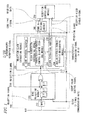
- Fig. 1 is a block diagram showing the embodiment of the invention.
- the components which are common to Fig. 7 are denoted by the same reference numerals.
- Figs. 1 and 7 are different from each other in the configuration of the reception clock extracting module 230.
- the reception clock extracting module 230 in Fig. 1 namely, an edge interval counter 233, an analog-circuit characteristic designating module 234, and a clock extraction controlling module 235 to which a function different from that in Fig. 7 is provided are disposed in addition to the clock extraction counter 232.
- the edge interval counter 233 counts intervals of edges which is detected and output by the edge detecting module 220, and supplies the count data to the clock extraction controlling module 235.
- the analog-circuit characteristic designating module 234 supplies a control signal for extracting clocks corresponding to the designated analog characteristics, to the clock extraction controlling module 235.
- the analog characteristics of the MAU 210 are at least one of: the rise delay characteristics in which the rising time of the reception signal is longer than the falling time; and the fall delay characteristics in which the falling time of the reception signal is longer than the rising time.
- the clock extraction controlling module 235 includes a characteristic-based control element storing module 236 which controls a predetermined clock extracting operation so as to be performed based on the analog characteristics of the MAU 210 that are designated through the analog-circuit characteristic designating module 234.
- the clock extraction counter 232 executes a predetermined counting operation based on a count value control signal which is output from the clock extraction controlling module 235.
- a related-art method of adjusting a count value is an adjusting method in which, when the edge position leads an ideal position, as shown in Fig. 15 , the count up operation is increased from the normal value of +1 by 1 to be set as +2, and, when the edge position lags, the count up operation is decreased from the normal value of +1 by 1 to be set as ⁇ 0. Therefore, the distance from the edge detection position to the sampling position (reception clock position) is not constant.
- the count value of the clock extraction counter 232 is adjusted while changing the follow-up width to the edge position according to the deviation width of the edge position, and therefore the lower (N - 1) bits of the count value subsequent to the edge detection position is always 1.
- the distance from the edge detection position to the sampling position is always constant (see Fig. 4 ).
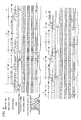
- the specific count value adjusting method for realizing this is as indicated in the tables of Figs. 2 and 3 .
- a signal of 1 bit time of communication data must be sampled once at 1/2 bit time, and twice at 1 bit time.
- the output of the reception clock signal is suppressed, and sampling is skipped with respect to a sampling position which is at a constant distance from the edge detection position.
- the certain conditions indicate the following two conditions for inhibiting sampling in order to correctly acquire a Manchester code:
- a Manchester code having the analog circuit characteristics of a) or b) described in the paragraph [0036] can be sampled once at 1/2 bit time, and twice at 1 bit time, and the Manchester code can be correctly acquired.
- Specific reception clock output suppressing conditions for realizing this are (a-1), (a-2) and (b-1), (b-2) which will be described later.
- the reception signal which is transmitted through the transmission path 100 is converted to a Manchester code by the MAU 210, and then supplied to the edge detecting module 220.
- CLK clock signal
- the clock extraction controlling module 235 produces and outputs the count value control signal for adjusting the count value so as to operate following with the edge position which is detected by the count up operation of the clock extraction counter 232.
- the count value is adjusted in the following manner.
- the count up operation is further advanced (+2) from the normal value (+1) by 1, and, when the edge position lags, the count up operation is further delayed ( ⁇ 0) from the normal value (+1) by 1,
- the distance from the edge position (the position of the edge detection signal) to the sampling position (the position of the reception clock position) is not constant, and hence the sampling position of the synchronized reception signal cannot be identified.
- the follow-up width which follows the edge position of the synchronized reception signal is changed according to the deviation width of the edge position.
- the count value is adjusted in accordance with a table such as shown in Fig. 2 .
- the lower (N - 1) bits of the count value of the clock extraction counter 232 which is subsequent to the edge detection position where the edge detection signal becomes active (High) is always 1. Therefore, the time from the edge position (the position of the edge detection signal) to the sampling position (the position of the reception clock position) is always constant (the points of 4*Tclk, 12*Tclk, 20*Tclk, ... from the edge position), and hence the sampling position of the synchronized reception signal can be identified.
- the clock extraction counter 232 outputs the reception clock signal at a cycle in which "the value of the lower (N - 1) bits of the clock extraction counter 232 at the current clock (CLK) cycle is 2 N-2 - 1" and "the value of the lower (N - 1) bits of the clock extraction counter 232 at the next clock is 2 N-2 ".
- the reception clock signal has a frequency which is two times the communication rate.
- the clock extraction counter 232 supplies the most significant bit of the clock extraction counter 232, as the reception clock enable signal to the reception controlling module 250.
- the code detecting module 240 samples the synchronized reception signal at the rising of the clock (CLK) during the High period of the reception clock signal, and performs decoding to recognize the type of the communication data.
- the adjustment of the count value according to the table of Fig. 2 is a basic adjustment.
- the reception jitter tolerance (limitation of jitter) becomes (2 N-2 - 1)*Tclk.
- the count value of the clock extraction counter 232 is adjusted as indicated by hatching the count value.
- the analog circuit which outputs the Manchester code has the above-described characteristics a) or b).
- Td within 1*Tclk
- the pulse width of the Manchester code which is input to a digital circuit becomes as described below, and the reception jitter tolerance cannot satisfy (2 N-2 - 1)*Tclk.
- the edge interval counter 233 is supplied to the clock extraction controlling module 235, and conditions for the reception clock output are added.
- the edge interval counter 233 is a counter in which, at the timing when the edge detection signal becomes active (High), the count value is initialized to 0, and, at the other timings, the count value is simply incremented (+1). The conditions to be added are as described below.
- the fact that the analog circuit has the characteristics a) is designated from the outside into the characteristic-based control element storing module 236 through the analog-circuit characteristic designating module 234. Then, a characteristic-based control element which performs a control so as to execute a clock extracting operation corresponding to the characteristics a) is read from the characteristic-based control element storing module 236 into the clock extraction controlling module 235.
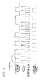
- the timings of t4 + 20*Tclk and t6 + 20*Tclk in the timing chart of Fig. 5 correspond to the conditions.
- the state where the conditions hold corresponds to the third sampling point in 1 bit time of the communication data, and the reception clock signal is not necessary for acquiring the correct value.
- Timing of t2 + 12*Tclk in the timing chart of Fig. 5 corresponds to the conditions.
- the value of the edge interval counter 233 is 2 N-1 + 2 N-2 - 2
- the edge detection signal is active (High) in the next cycle
- the synchronized reception signal is Low.
- the state where the conditions hold corresponds to the second sampling point in 1/2 bit time of the communication data, and the reception clock signal is not necessary for acquiring the correct value.
- the reception clock signal is output in accordance with the condition of (5).
- the fact that the analog circuit has the characteristics b) is designated from the outside into the characteristic-based control element storing module 236 through the analog-circuit characteristic designating module 234. Then, a characteristic-based control element which performs a control so as to execute a clock extracting operation corresponding to the characteristics b) is read from the characteristic-based control element storing module 236 into the clock extraction controlling module 235.
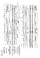
- the timing of t3 + 20*Tclk in the timing chart of Fig. 6 corresponds to the conditions.
- the state where the conditions hold corresponds to the third sampling point in 1 bit time of the communication data, and the reception clock signal is not necessary for acquiring the correct value.
- Timings of t1 + 12*Tclk and t5 + 12*Tclk in the timing chart of Fig. 6 correspond to the conditions.
- the value of the edge interval counter is 2 N-1 + 2 N-2 - 2
- the edge detection signal is active (High) in the next cycle
- the synchronized reception signal is High
- the state where the conditions hold corresponds to the second sampling point in 1/2 bit time of the communication data, and the reception clock signal is not necessary for acquiring the correct value.
- the reception clock signal is output in accordance with the condition of (5).
- reception clock output control When the above-described reception clock output control is performed, also a reception signal of jitter of (2 N-2 - 1)*Tclk having the analog circuit characteristics of a) or b) can be sampled twice per 1 bit time (once per 1/2 bit time), and the reception signal can be correctly sampled.
- Received data of the code type, "1", and "0" are output to the reception controlling module 250 which is in the subsequent stage, and which performs a reception control.
- the timing chart of Fig. 6 shows a similar case where the analog circuit has the characteristics of b).
Landscapes
- Engineering & Computer Science (AREA)
- Computer Networks & Wireless Communication (AREA)
- Signal Processing (AREA)
- Physics & Mathematics (AREA)
- Spectroscopy & Molecular Physics (AREA)
- Theoretical Computer Science (AREA)
- Dc Digital Transmission (AREA)
- Synchronisation In Digital Transmission Systems (AREA)
Applications Claiming Priority (2)
| Application Number | Priority Date | Filing Date | Title |
|---|---|---|---|
| JP2012276848 | 2012-12-19 | ||
| JP2013185094A JP5700091B2 (ja) | 2012-12-19 | 2013-09-06 | マンチェスターコード受信回路 |
Publications (3)
| Publication Number | Publication Date |
|---|---|
| EP2747291A2 true EP2747291A2 (de) | 2014-06-25 |
| EP2747291A3 EP2747291A3 (de) | 2016-04-13 |
| EP2747291B1 EP2747291B1 (de) | 2019-11-27 |
Family
ID=50023386
Family Applications (1)
| Application Number | Title | Priority Date | Filing Date |
|---|---|---|---|
| EP13198621.8A Active EP2747291B1 (de) | 2012-12-19 | 2013-12-19 | Manchester Code Empfangsschaltung |
Country Status (4)
| Country | Link |
|---|---|
| US (1) | US9083505B2 (de) |
| EP (1) | EP2747291B1 (de) |
| JP (1) | JP5700091B2 (de) |
| CN (1) | CN103888143B (de) |
Cited By (1)
| Publication number | Priority date | Publication date | Assignee | Title |
|---|---|---|---|---|
| CN106302022A (zh) * | 2016-08-19 | 2017-01-04 | 凌云科技集团有限责任公司 | 一种机载大气数据系统曼彻斯特码解析及仿真系统 |
Families Citing this family (6)
| Publication number | Priority date | Publication date | Assignee | Title |
|---|---|---|---|---|
| KR102329802B1 (ko) | 2015-07-23 | 2021-11-22 | 삼성전자주식회사 | 테스트 인터페이스 보드, 테스트 장비, 테스트 시스템 및 테스트 방법 |
| TWI615700B (zh) * | 2015-10-14 | 2018-02-21 | 慧榮科技股份有限公司 | 時脈校正方法、參考時脈產生方法、時脈校正電路以及參考時脈產生電路 |
| CN106911324A (zh) * | 2015-12-23 | 2017-06-30 | 华大半导体有限公司 | 一种高频标签的ppm解码方法 |
| KR102507862B1 (ko) * | 2018-07-09 | 2023-03-08 | 주식회사 엘엑스세미콘 | 인터페이스신호에서 임베디드클럭을 복원하는 클럭복원장치 및 소스드라이버 |
| CN112491446B (zh) * | 2021-02-05 | 2021-06-04 | 苏州裕太微电子有限公司 | 一种有线通信抗干扰方法及系统 |
| CN119382712B (zh) * | 2024-12-31 | 2025-03-11 | 青岛本原微电子有限公司 | 一种曼彻斯特解码系统及解码方法 |
Family Cites Families (7)
| Publication number | Priority date | Publication date | Assignee | Title |
|---|---|---|---|---|
| US5805632A (en) * | 1992-11-19 | 1998-09-08 | Cirrus Logic, Inc. | Bit rate doubler for serial data transmission or storage |
| JP2911748B2 (ja) | 1994-05-31 | 1999-06-23 | 株式会社日立製作所 | フィールドバスシステムにおける通信装置 |
| US5726650A (en) * | 1995-06-07 | 1998-03-10 | Silicon Systems, Inc. | Adaptive manchester decoding with adjustable delay and power saving mode |
| US7382845B1 (en) * | 2001-12-14 | 2008-06-03 | Symmetricom, Inc. | Distribution of synchronization in an ethernet local area network environment |
| EP1335520B1 (de) | 2002-02-11 | 2018-05-30 | Semiconductor Components Industries, LLC | Multiplex-bussystem mit tastverhältniskorrektur |
| DE102006011059A1 (de) | 2006-03-08 | 2007-09-13 | Robert Bosch Gmbh | Verfahren und System zum Übertragen von in einem Signal codierten Daten |
| JP4947173B2 (ja) | 2010-03-16 | 2012-06-06 | 横河電機株式会社 | 交流インピーダンス測定装置 |
-
2013
- 2013-09-06 JP JP2013185094A patent/JP5700091B2/ja active Active
- 2013-12-18 US US14/132,006 patent/US9083505B2/en active Active
- 2013-12-19 EP EP13198621.8A patent/EP2747291B1/de active Active
- 2013-12-19 CN CN201310706069.1A patent/CN103888143B/zh active Active
Non-Patent Citations (1)
| Title |
|---|
| None |
Cited By (2)
| Publication number | Priority date | Publication date | Assignee | Title |
|---|---|---|---|---|
| CN106302022A (zh) * | 2016-08-19 | 2017-01-04 | 凌云科技集团有限责任公司 | 一种机载大气数据系统曼彻斯特码解析及仿真系统 |
| CN106302022B (zh) * | 2016-08-19 | 2019-05-14 | 凌云科技集团有限责任公司 | 一种机载大气数据系统曼彻斯特码解析及仿真系统 |
Also Published As
| Publication number | Publication date |
|---|---|
| EP2747291B1 (de) | 2019-11-27 |
| EP2747291A3 (de) | 2016-04-13 |
| US20140169507A1 (en) | 2014-06-19 |
| JP5700091B2 (ja) | 2015-04-15 |
| CN103888143B (zh) | 2017-08-08 |
| JP2014140153A (ja) | 2014-07-31 |
| CN103888143A (zh) | 2014-06-25 |
| US9083505B2 (en) | 2015-07-14 |
Similar Documents
| Publication | Publication Date | Title |
|---|---|---|
| US9083505B2 (en) | Manchester code receiving circuit | |
| US7920601B2 (en) | Vehicular communications system having improved serial communication | |
| JP6697990B2 (ja) | 半導体装置 | |
| EP1704457B1 (de) | Einrichtung mit verbesserter serieller kommunikation | |
| US8842793B2 (en) | Communication circuit and method of adjusting sampling clock signal | |
| US8565296B2 (en) | Adaptive receiver system and adaptive transceiver system | |
| EP3422626B1 (de) | Demodulator für pulsweitenmodulierte taktsignale | |
| EP3912303B1 (de) | Abtastpunktbestimmung für asynchrone datenerfassung mit niedriger frequenz | |
| US20110026572A1 (en) | Baud rate error detection circuit and baud rate error detection method | |
| KR20140079083A (ko) | 듀티 사이클 보정 장치 및 방법, 그리고 그를 이용하는 수신기 | |
| JP2017135506A (ja) | スキュー調整回路、半導体装置およびスキューキャリブレーション方法 | |
| US9654114B2 (en) | Transmission circuit, integrated circuit, and parallel-to-serial conversion method | |
| US7167034B2 (en) | Arrangement for correcting the phase of a data sampling clock signal during a period of sampling data in a received signal | |
| US20060193414A1 (en) | Synchronization and data recovery device | |
| US6597296B2 (en) | Center phase verifying circuit and center phase verifying method | |
| US5901181A (en) | Circuit for restoring bits transmitted by a series signal | |
| CN110719071B (zh) | 一种带有校准的倍频电路以及控制方法 | |
| US10033525B2 (en) | Transmission device and signal processing method | |
| WO2022081559A1 (en) | Dynamic timing calibration systems and methods | |
| US9350529B1 (en) | Method and apparatus for detecting logical signal | |
| JP2014003375A (ja) | データ受信回路 | |
| CN120825173B (zh) | 一种模数转换器动态时钟相位校准与同步系统 | |
| KR102856507B1 (ko) | 타임-인터리브 adc의 타이밍 스큐 불일치 교정 방법 | |
| JPWO2006120746A1 (ja) | Pll回路およびその設計方法 | |
| WO2017213138A1 (ja) | 受信装置 |
Legal Events
| Date | Code | Title | Description |
|---|---|---|---|
| PUAI | Public reference made under article 153(3) epc to a published international application that has entered the european phase |
Free format text: ORIGINAL CODE: 0009012 |
|
| 17P | Request for examination filed |
Effective date: 20131219 |
|
| AK | Designated contracting states |
Kind code of ref document: A2 Designated state(s): AL AT BE BG CH CY CZ DE DK EE ES FI FR GB GR HR HU IE IS IT LI LT LU LV MC MK MT NL NO PL PT RO RS SE SI SK SM TR |
|
| AX | Request for extension of the european patent |
Extension state: BA ME |
|
| PUAL | Search report despatched |
Free format text: ORIGINAL CODE: 0009013 |
|
| AK | Designated contracting states |
Kind code of ref document: A3 Designated state(s): AL AT BE BG CH CY CZ DE DK EE ES FI FR GB GR HR HU IE IS IT LI LT LU LV MC MK MT NL NO PL PT RO RS SE SI SK SM TR |
|
| AX | Request for extension of the european patent |
Extension state: BA ME |
|
| RIC1 | Information provided on ipc code assigned before grant |
Ipc: H03M 5/12 20060101AFI20160304BHEP Ipc: H04L 25/49 20060101ALI20160304BHEP |
|
| R17P | Request for examination filed (corrected) |
Effective date: 20161013 |
|
| RBV | Designated contracting states (corrected) |
Designated state(s): AL AT BE BG CH CY CZ DE DK EE ES FI FR GB GR HR HU IE IS IT LI LT LU LV MC MK MT NL NO PL PT RO RS SE SI SK SM TR |
|
| STAA | Information on the status of an ep patent application or granted ep patent |
Free format text: STATUS: EXAMINATION IS IN PROGRESS |
|
| 17Q | First examination report despatched |
Effective date: 20181016 |
|
| GRAP | Despatch of communication of intention to grant a patent |
Free format text: ORIGINAL CODE: EPIDOSNIGR1 |
|
| STAA | Information on the status of an ep patent application or granted ep patent |
Free format text: STATUS: GRANT OF PATENT IS INTENDED |
|
| INTG | Intention to grant announced |
Effective date: 20190604 |
|
| RIN1 | Information on inventor provided before grant (corrected) |
Inventor name: SHIMADA, KATSUYUKI |
|
| GRAS | Grant fee paid |
Free format text: ORIGINAL CODE: EPIDOSNIGR3 |
|
| GRAA | (expected) grant |
Free format text: ORIGINAL CODE: 0009210 |
|
| STAA | Information on the status of an ep patent application or granted ep patent |
Free format text: STATUS: THE PATENT HAS BEEN GRANTED |
|
| AK | Designated contracting states |
Kind code of ref document: B1 Designated state(s): AL AT BE BG CH CY CZ DE DK EE ES FI FR GB GR HR HU IE IS IT LI LT LU LV MC MK MT NL NO PL PT RO RS SE SI SK SM TR |
|
| REG | Reference to a national code |
Ref country code: GB Ref legal event code: FG4D |
|
| REG | Reference to a national code |
Ref country code: CH Ref legal event code: EP |
|
| REG | Reference to a national code |
Ref country code: AT Ref legal event code: REF Ref document number: 1207883 Country of ref document: AT Kind code of ref document: T Effective date: 20191215 |
|
| REG | Reference to a national code |
Ref country code: DE Ref legal event code: R096 Ref document number: 602013063317 Country of ref document: DE |
|
| REG | Reference to a national code |
Ref country code: IE Ref legal event code: FG4D |
|
| REG | Reference to a national code |
Ref country code: NL Ref legal event code: MP Effective date: 20191127 |
|
| REG | Reference to a national code |
Ref country code: LT Ref legal event code: MG4D |
|
| PG25 | Lapsed in a contracting state [announced via postgrant information from national office to epo] |
Ref country code: FI Free format text: LAPSE BECAUSE OF FAILURE TO SUBMIT A TRANSLATION OF THE DESCRIPTION OR TO PAY THE FEE WITHIN THE PRESCRIBED TIME-LIMIT Effective date: 20191127 Ref country code: BG Free format text: LAPSE BECAUSE OF FAILURE TO SUBMIT A TRANSLATION OF THE DESCRIPTION OR TO PAY THE FEE WITHIN THE PRESCRIBED TIME-LIMIT Effective date: 20200227 Ref country code: NO Free format text: LAPSE BECAUSE OF FAILURE TO SUBMIT A TRANSLATION OF THE DESCRIPTION OR TO PAY THE FEE WITHIN THE PRESCRIBED TIME-LIMIT Effective date: 20200227 Ref country code: GR Free format text: LAPSE BECAUSE OF FAILURE TO SUBMIT A TRANSLATION OF THE DESCRIPTION OR TO PAY THE FEE WITHIN THE PRESCRIBED TIME-LIMIT Effective date: 20200228 Ref country code: LT Free format text: LAPSE BECAUSE OF FAILURE TO SUBMIT A TRANSLATION OF THE DESCRIPTION OR TO PAY THE FEE WITHIN THE PRESCRIBED TIME-LIMIT Effective date: 20191127 Ref country code: NL Free format text: LAPSE BECAUSE OF FAILURE TO SUBMIT A TRANSLATION OF THE DESCRIPTION OR TO PAY THE FEE WITHIN THE PRESCRIBED TIME-LIMIT Effective date: 20191127 Ref country code: ES Free format text: LAPSE BECAUSE OF FAILURE TO SUBMIT A TRANSLATION OF THE DESCRIPTION OR TO PAY THE FEE WITHIN THE PRESCRIBED TIME-LIMIT Effective date: 20191127 Ref country code: SE Free format text: LAPSE BECAUSE OF FAILURE TO SUBMIT A TRANSLATION OF THE DESCRIPTION OR TO PAY THE FEE WITHIN THE PRESCRIBED TIME-LIMIT Effective date: 20191127 Ref country code: LV Free format text: LAPSE BECAUSE OF FAILURE TO SUBMIT A TRANSLATION OF THE DESCRIPTION OR TO PAY THE FEE WITHIN THE PRESCRIBED TIME-LIMIT Effective date: 20191127 |
|
| PG25 | Lapsed in a contracting state [announced via postgrant information from national office to epo] |
Ref country code: IS Free format text: LAPSE BECAUSE OF FAILURE TO SUBMIT A TRANSLATION OF THE DESCRIPTION OR TO PAY THE FEE WITHIN THE PRESCRIBED TIME-LIMIT Effective date: 20200327 Ref country code: RS Free format text: LAPSE BECAUSE OF FAILURE TO SUBMIT A TRANSLATION OF THE DESCRIPTION OR TO PAY THE FEE WITHIN THE PRESCRIBED TIME-LIMIT Effective date: 20191127 Ref country code: HR Free format text: LAPSE BECAUSE OF FAILURE TO SUBMIT A TRANSLATION OF THE DESCRIPTION OR TO PAY THE FEE WITHIN THE PRESCRIBED TIME-LIMIT Effective date: 20191127 |
|
| PG25 | Lapsed in a contracting state [announced via postgrant information from national office to epo] |
Ref country code: AL Free format text: LAPSE BECAUSE OF FAILURE TO SUBMIT A TRANSLATION OF THE DESCRIPTION OR TO PAY THE FEE WITHIN THE PRESCRIBED TIME-LIMIT Effective date: 20191127 |
|
| PG25 | Lapsed in a contracting state [announced via postgrant information from national office to epo] |
Ref country code: DK Free format text: LAPSE BECAUSE OF FAILURE TO SUBMIT A TRANSLATION OF THE DESCRIPTION OR TO PAY THE FEE WITHIN THE PRESCRIBED TIME-LIMIT Effective date: 20191127 Ref country code: RO Free format text: LAPSE BECAUSE OF FAILURE TO SUBMIT A TRANSLATION OF THE DESCRIPTION OR TO PAY THE FEE WITHIN THE PRESCRIBED TIME-LIMIT Effective date: 20191127 Ref country code: CZ Free format text: LAPSE BECAUSE OF FAILURE TO SUBMIT A TRANSLATION OF THE DESCRIPTION OR TO PAY THE FEE WITHIN THE PRESCRIBED TIME-LIMIT Effective date: 20191127 Ref country code: PT Free format text: LAPSE BECAUSE OF FAILURE TO SUBMIT A TRANSLATION OF THE DESCRIPTION OR TO PAY THE FEE WITHIN THE PRESCRIBED TIME-LIMIT Effective date: 20200419 Ref country code: EE Free format text: LAPSE BECAUSE OF FAILURE TO SUBMIT A TRANSLATION OF THE DESCRIPTION OR TO PAY THE FEE WITHIN THE PRESCRIBED TIME-LIMIT Effective date: 20191127 |
|
| REG | Reference to a national code |
Ref country code: CH Ref legal event code: PL |
|
| REG | Reference to a national code |
Ref country code: BE Ref legal event code: MM Effective date: 20191231 |
|
| REG | Reference to a national code |
Ref country code: DE Ref legal event code: R097 Ref document number: 602013063317 Country of ref document: DE |
|
| PG25 | Lapsed in a contracting state [announced via postgrant information from national office to epo] |
Ref country code: MC Free format text: LAPSE BECAUSE OF FAILURE TO SUBMIT A TRANSLATION OF THE DESCRIPTION OR TO PAY THE FEE WITHIN THE PRESCRIBED TIME-LIMIT Effective date: 20191127 Ref country code: SK Free format text: LAPSE BECAUSE OF FAILURE TO SUBMIT A TRANSLATION OF THE DESCRIPTION OR TO PAY THE FEE WITHIN THE PRESCRIBED TIME-LIMIT Effective date: 20191127 Ref country code: SM Free format text: LAPSE BECAUSE OF FAILURE TO SUBMIT A TRANSLATION OF THE DESCRIPTION OR TO PAY THE FEE WITHIN THE PRESCRIBED TIME-LIMIT Effective date: 20191127 |
|
| REG | Reference to a national code |
Ref country code: AT Ref legal event code: MK05 Ref document number: 1207883 Country of ref document: AT Kind code of ref document: T Effective date: 20191127 |
|
| PLBE | No opposition filed within time limit |
Free format text: ORIGINAL CODE: 0009261 |
|
| STAA | Information on the status of an ep patent application or granted ep patent |
Free format text: STATUS: NO OPPOSITION FILED WITHIN TIME LIMIT |
|
| GBPC | Gb: european patent ceased through non-payment of renewal fee |
Effective date: 20200227 |
|
| PG25 | Lapsed in a contracting state [announced via postgrant information from national office to epo] |
Ref country code: LU Free format text: LAPSE BECAUSE OF NON-PAYMENT OF DUE FEES Effective date: 20191219 Ref country code: FR Free format text: LAPSE BECAUSE OF NON-PAYMENT OF DUE FEES Effective date: 20200127 Ref country code: IE Free format text: LAPSE BECAUSE OF NON-PAYMENT OF DUE FEES Effective date: 20191219 |
|
| 26N | No opposition filed |
Effective date: 20200828 |
|
| PG25 | Lapsed in a contracting state [announced via postgrant information from national office to epo] |
Ref country code: PL Free format text: LAPSE BECAUSE OF FAILURE TO SUBMIT A TRANSLATION OF THE DESCRIPTION OR TO PAY THE FEE WITHIN THE PRESCRIBED TIME-LIMIT Effective date: 20191127 Ref country code: LI Free format text: LAPSE BECAUSE OF NON-PAYMENT OF DUE FEES Effective date: 20191231 Ref country code: CH Free format text: LAPSE BECAUSE OF NON-PAYMENT OF DUE FEES Effective date: 20191231 Ref country code: SI Free format text: LAPSE BECAUSE OF FAILURE TO SUBMIT A TRANSLATION OF THE DESCRIPTION OR TO PAY THE FEE WITHIN THE PRESCRIBED TIME-LIMIT Effective date: 20191127 Ref country code: AT Free format text: LAPSE BECAUSE OF FAILURE TO SUBMIT A TRANSLATION OF THE DESCRIPTION OR TO PAY THE FEE WITHIN THE PRESCRIBED TIME-LIMIT Effective date: 20191127 Ref country code: BE Free format text: LAPSE BECAUSE OF NON-PAYMENT OF DUE FEES Effective date: 20191231 |
|
| PG25 | Lapsed in a contracting state [announced via postgrant information from national office to epo] |
Ref country code: GB Free format text: LAPSE BECAUSE OF NON-PAYMENT OF DUE FEES Effective date: 20200227 Ref country code: IT Free format text: LAPSE BECAUSE OF FAILURE TO SUBMIT A TRANSLATION OF THE DESCRIPTION OR TO PAY THE FEE WITHIN THE PRESCRIBED TIME-LIMIT Effective date: 20191127 |
|
| PG25 | Lapsed in a contracting state [announced via postgrant information from national office to epo] |
Ref country code: CY Free format text: LAPSE BECAUSE OF FAILURE TO SUBMIT A TRANSLATION OF THE DESCRIPTION OR TO PAY THE FEE WITHIN THE PRESCRIBED TIME-LIMIT Effective date: 20191127 |
|
| PG25 | Lapsed in a contracting state [announced via postgrant information from national office to epo] |
Ref country code: MT Free format text: LAPSE BECAUSE OF FAILURE TO SUBMIT A TRANSLATION OF THE DESCRIPTION OR TO PAY THE FEE WITHIN THE PRESCRIBED TIME-LIMIT Effective date: 20191127 Ref country code: HU Free format text: LAPSE BECAUSE OF FAILURE TO SUBMIT A TRANSLATION OF THE DESCRIPTION OR TO PAY THE FEE WITHIN THE PRESCRIBED TIME-LIMIT; INVALID AB INITIO Effective date: 20131219 |
|
| PG25 | Lapsed in a contracting state [announced via postgrant information from national office to epo] |
Ref country code: TR Free format text: LAPSE BECAUSE OF FAILURE TO SUBMIT A TRANSLATION OF THE DESCRIPTION OR TO PAY THE FEE WITHIN THE PRESCRIBED TIME-LIMIT Effective date: 20191127 |
|
| PG25 | Lapsed in a contracting state [announced via postgrant information from national office to epo] |
Ref country code: MK Free format text: LAPSE BECAUSE OF FAILURE TO SUBMIT A TRANSLATION OF THE DESCRIPTION OR TO PAY THE FEE WITHIN THE PRESCRIBED TIME-LIMIT Effective date: 20191127 |
|
| P01 | Opt-out of the competence of the unified patent court (upc) registered |
Effective date: 20230603 |
|
| PGFP | Annual fee paid to national office [announced via postgrant information from national office to epo] |
Ref country code: DE Payment date: 20251126 Year of fee payment: 13 |