EP2745478B1 - Schaltungsanordnung und verfahren zum übertragen von signalen - Google Patents
Schaltungsanordnung und verfahren zum übertragen von signalen Download PDFInfo
- Publication number
- EP2745478B1 EP2745478B1 EP12813749.4A EP12813749A EP2745478B1 EP 2745478 B1 EP2745478 B1 EP 2745478B1 EP 12813749 A EP12813749 A EP 12813749A EP 2745478 B1 EP2745478 B1 EP 2745478B1
- Authority
- EP
- European Patent Office
- Prior art keywords
- signals
- data
- clock
- data signals
- clock signals
- Prior art date
- Legal status (The legal status is an assumption and is not a legal conclusion. Google has not performed a legal analysis and makes no representation as to the accuracy of the status listed.)
- Active
Links
Images

Classifications
-
- H—ELECTRICITY
- H04—ELECTRIC COMMUNICATION TECHNIQUE
- H04L—TRANSMISSION OF DIGITAL INFORMATION, e.g. TELEGRAPHIC COMMUNICATION
- H04L7/00—Arrangements for synchronising receiver with transmitter
- H04L7/04—Speed or phase control by synchronisation signals
- H04L7/048—Speed or phase control by synchronisation signals using the properties of error detecting or error correcting codes, e.g. parity as synchronisation signal
-
- H—ELECTRICITY
- H04—ELECTRIC COMMUNICATION TECHNIQUE
- H04L—TRANSMISSION OF DIGITAL INFORMATION, e.g. TELEGRAPHIC COMMUNICATION
- H04L25/00—Baseband systems
- H04L25/02—Details ; arrangements for supplying electrical power along data transmission lines
- H04L25/0264—Arrangements for coupling to transmission lines
- H04L25/0272—Arrangements for coupling to multiple lines, e.g. for differential transmission
- H04L25/0276—Arrangements for coupling common mode signals
-
- G—PHYSICS
- G06—COMPUTING OR CALCULATING; COUNTING
- G06F—ELECTRIC DIGITAL DATA PROCESSING
- G06F1/00—Details not covered by groups G06F3/00 - G06F13/00 and G06F21/00
- G06F1/04—Generating or distributing clock signals or signals derived directly therefrom
- G06F1/10—Distribution of clock signals, e.g. skew
- G06F1/105—Distribution of clock signals, e.g. skew in which the distribution is at least partially optical
-
- H—ELECTRICITY
- H04—ELECTRIC COMMUNICATION TECHNIQUE
- H04L—TRANSMISSION OF DIGITAL INFORMATION, e.g. TELEGRAPHIC COMMUNICATION
- H04L7/00—Arrangements for synchronising receiver with transmitter
- H04L7/0091—Transmitter details
-
- G—PHYSICS
- G06—COMPUTING OR CALCULATING; COUNTING
- G06F—ELECTRIC DIGITAL DATA PROCESSING
- G06F1/00—Details not covered by groups G06F3/00 - G06F13/00 and G06F21/00
- G06F1/04—Generating or distributing clock signals or signals derived directly therefrom
-
- H—ELECTRICITY
- H04—ELECTRIC COMMUNICATION TECHNIQUE
- H04L—TRANSMISSION OF DIGITAL INFORMATION, e.g. TELEGRAPHIC COMMUNICATION
- H04L7/00—Arrangements for synchronising receiver with transmitter
- H04L7/0008—Synchronisation information channels, e.g. clock distribution lines
Definitions
- the present invention relates to a circuit arrangement according to the preamble of claim 1 and a method according to the preamble of claim 11.
- the bit transmission layer or physical layer is the lowest layer in the O [pen] S [ystems] I [nterconnection] layer model, which is also called the OSI reference model and a layer model of the International Organization for Standardization (ISO), which in turn serves as a design basis for communication protocols in computer networks.
- ISO International Organization for Standardization
- the physical layer is responsible for combining, forward] e [rror] correction], modulation, power control, spreading (C [ode] D [ivision] M [ultiple] A [ccess]) and the like and knows neither data nor applications, only zeros and ones.
- PHY provides the overlying security layer (D [ata] L [ink] L [ayer]), in particular a sublayer called M [edia] A [ccess] C [ontrol] layer, logical channels (transport channels in the case of Universal ] M [obile] T [elecommunications] S [ystem]).
- D-PHY basically enables a flexible, inexpensive and fast serial interface for communication connections between components within a mobile device.
- FIG. 3A provides a data source in modern mobile phones, for example an application processor, on the M [obile] I [ndustry] P [rocessor] I [nterface] -D [isplay] S [erial] I [nterface] image data as D-PHY- Signals for display on a connected data sink, for example on a connected display, are available.
- a data sink for example an application processor, can also receive image data from a connected data source, for example from a connected camera, in D-PHY format via a MIPI-C [amera] S [erial] I [nterface].
- a DSI or DSI-2 or CSI or CSI-2 or CSI-3 based on the D-PHY protocol comprises up to four differential data lines and a differential clock line that electrically connects the application processor to the display and / or the camera using copper cables connect.
- the data rate per differential data line is up to 1.5 Gbps (gigabits per second).
- the SL83014 includes a galvanic connection that can be used for bidirectional LP data transmission.
- the object of the present invention is to further develop a circuit arrangement of the type mentioned and a method of the type mentioned so that a further
- the various signals for the transport taking place between the transmitting arrangement and the receiving arrangement via at least one optical medium in particular via at least one optical waveguide, for example via at least one glass fiber and / or via at least one plastic fiber, can be processed into a common signal stream, in particular bundled on the transmission side or serialized and unbundled or deserialized at the receiving end.
- a common signal stream bundled or serialized according to the transmission arrangement set out above can be recorded on the side of the receiving arrangement in order to use it to generate the at least one, in particular the up to four, differential data lines and to recover the at least one, in particular exactly one, differential clock line for the DSI, also in the DSI-2 specification, and / or for the CSI, also in the CSI-2 and / or CSI-3 specifications, in particular by unbundling.
- the optical transmission does not generate any high-frequency electromagnetic fields that could affect sensitive neighboring receivers of high-frequency useful signals such as Bluetooth, global positioning, universal, mobile telecommunications ] S [ystem] or Wi-Fi receivers. This also does not impair their function.
- the number of transmission channels can be reduced to one optical waveguide per display and / or per camera.
- the present invention can be transmitted with simultaneous serial and / or bundled, in particular CSI-protocol-based and / or CSI-2-protocol-based and / or CSI-3-protocol-based and / or DSI-protocol-based and / or DSI-2-protocol-based, transmission both single-ended data and clock signals based on logic levels and differential data and clock signals, in particular data and clock signals based on common mode, in particular D-PHY data signals and D-PHY clock signals, for example of up to four bits wide MIPI-D-PHY data signals and MIPI-D-PHY clock signals, between at least one data source, in particular at least one, for example high-resolution and / or for example functioning as an image source, Camera and / or at least one application processor, and at least one data sink, in particular at least one application processor and / or at least one, for example high-resolution and / or for example acting as an image sink, display unit, for example at least one display or at least
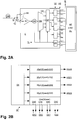
- Figure 1A shows an exemplary embodiment for the basic structure of a transmission arrangement S for connection to a D [display] S [erial] I [nterface] data transmission interface IS or also to a C [amera] S [erial] I [nterface] data transmission interface IS.
- the image data generated in the application processor AP or in the camera KA are transmitted on four data lines or channels CH0 +, CH0-, CH1 +, CH1-, CH2 +, CH2-, CH3 +, CH3- as D-PHY signals at the data transmission interface, which is up to four bits wide IS provided together with D-PHY-correct clock signals CLK +, CLK-.
- the transmission arrangement S receives these signals on an integrated interface logic LS, whose blocks each have at least one state machine for correct interpretation of the D-PHY logic signals and for differentiating between high-frequency data streams (so-called H [igh] S [peed] data) and low-frequency data streams (so-called L [ow] S [peed] data) can have.
- a framer FR following in the transmission arrangement S ensures the D [irect] C [urrent] balancing of the input signal and generates a signal on the receiving side (cf. Figure 2A ) recognizable frame, which the receiving arrangement E (cf. Figure 2A ) enables the received data to be reassigned to the correct output data lines or output channels CH0 +, CH0-, CH1 +, CH1-, CH2 +, CH2-, CH3 +, CH3-.
- the framer FR can according to Figure 1B both the single-ended data signals HSD0, HSD1, HSD2, HSD3 based on logic levels and the differential data signals DD0 +, DD0-, DD1 +, DD1-, DD2 +, DD2-, DD3 +, DD3- can be applied.
- the framer embeds FR in accordance with Figure 1B these differential data signals DD0 +, DD0-, DD1 +, DD1-, DD2 +, DD2-, DD3 +, DD3- in the stream of the single-ended, logic level-based data signals HSD0, HSD1, HSD2, HSD3.
- the framer FR and the multiplexer MU together form the serializer SE.
- the D-PHY clock signal provided via the clock port CLK +, CLK- and via the clock module CS of the interface logic LS by means of the clock generator PS serves as a (clock) reference for the serializer SE, in particular for its multiplexer MU, and is embedded in the serial data stream, i.e. in the serialized output signal. This creates the common signal current SI, which is sent to the receiving arrangement E (cf. Figure 2A ) is transmitted.
- the output driver AT is an integrated laser driver for controlling at least one directly connected laser LA, in particular for controlling at least one directly connected laser V [ertical] C [avity] S [urface] E [mitting] L [aserdiode].
- Figure 2A shows an exemplary embodiment for the basic structure of a receiving arrangement E for connection to a D [display] S [serial] I [nterface] data transmission interface IE or also to a C [amera] S [erial] I [nterface] data transmission interface IE.
- the transmission arrangement S (cf. Figure 1A ) sent serial or bundled data are received via an input amplifier EV of the receiving arrangement E and fed to an integrated clock and data recovery CD.
- This integrated clock and data recovery CD regenerates the original D-PHY clock from the common signal stream SI, which is transmitted directly to the D [display] S [erial] I [nterface] or the C [amera] via the clock module CE of the interface logic LE ] S [erial] I [nterface] will be made available again.
- the remaining serial data stream is unbundled and parallelized via a demultiplexer DM and sent to a deframer DF (cf. Figure 2B ), which is basically the mirror image of the framer FR in accordance with Figure 1B is constructed.
- the demultiplexer DM and the deframer DF together form the deserializer DS.
- the Deframer FR can according to Figure 2B the differential data signals DD0 +, DD0-, DD1 +, DD1-, DD2 +, DD2-, DD3 +, DD3- from the single-ended data signals HSD0, HSD1, HSD2, HSD3 based on logic levels by means of its decoder DK designed as a 6b / 5b decoder block separate and reassign the repaired data signals to the respectively applicable data lines CH0 +, CH0-, CH1 +, CH1-, CH2 +, CH2-, CH3 +, CH3-.
- the interface logic blocks LE shown in the receiving arrangement E can each have at least one state machine for correctly interpreting the D-PHY logic signals and for differentiating between high-frequency data streams and low-frequency data streams.
- the input amplifier EV is designed as an integrated transimpedance amplifier, which makes it possible to connect a photodiode FD directly to the receiving arrangement E.
- the cable-based multiplexed connection between the transmission arrangement S (cf. Figure 1A ) and the receiving arrangement E (cf. Figure 2A ) on an optical basis namely by means of an optical waveguide OM designed, for example, in the form of a glass fiber and / or in the form of a plastic fiber, and to operate it.
Landscapes
- Engineering & Computer Science (AREA)
- Computer Networks & Wireless Communication (AREA)
- Signal Processing (AREA)
- Theoretical Computer Science (AREA)
- Power Engineering (AREA)
- Physics & Mathematics (AREA)
- General Engineering & Computer Science (AREA)
- General Physics & Mathematics (AREA)
- Dc Digital Transmission (AREA)
- Optical Communication System (AREA)
- Logic Circuits (AREA)
Applications Claiming Priority (2)
| Application Number | Priority Date | Filing Date | Title |
|---|---|---|---|
| DE102011052764 | 2011-08-16 | ||
| PCT/DE2012/200054 WO2013023656A2 (de) | 2011-08-16 | 2012-08-16 | Schaltungsanordnung und verfahren zum übertragen von signalen |
Publications (2)
| Publication Number | Publication Date |
|---|---|
| EP2745478A2 EP2745478A2 (de) | 2014-06-25 |
| EP2745478B1 true EP2745478B1 (de) | 2021-03-10 |
Family
ID=47556997
Family Applications (1)
| Application Number | Title | Priority Date | Filing Date |
|---|---|---|---|
| EP12813749.4A Active EP2745478B1 (de) | 2011-08-16 | 2012-08-16 | Schaltungsanordnung und verfahren zum übertragen von signalen |
Country Status (5)
| Country | Link |
|---|---|
| US (1) | US9231756B2 (enExample) |
| EP (1) | EP2745478B1 (enExample) |
| JP (1) | JP6126603B2 (enExample) |
| DE (1) | DE112012003363A5 (enExample) |
| WO (1) | WO2013023656A2 (enExample) |
Family Cites Families (10)
| Publication number | Priority date | Publication date | Assignee | Title |
|---|---|---|---|---|
| JP2001103028A (ja) * | 1999-10-01 | 2001-04-13 | Nippon Telegr & Teleph Corp <Ntt> | 信号多重方法 |
| US7587537B1 (en) * | 2007-11-30 | 2009-09-08 | Altera Corporation | Serializer-deserializer circuits formed from input-output circuit registers |
| JP4633547B2 (ja) * | 2004-06-18 | 2011-02-16 | パナソニック株式会社 | 携帯情報端末機器およびその機器内相互通信方法 |
| KR101030768B1 (ko) * | 2004-08-26 | 2011-04-27 | 삼성전자주식회사 | 소비전력이 적고 고주파 동작이 가능한 광범위 지연동기루프 회로 및 이를 구비하는 광학 구동 시스템 |
| JP5223183B2 (ja) * | 2006-10-31 | 2013-06-26 | 日立電線株式会社 | 光電気複合配線部品及びこれを用いた電子機器 |
| JP2008160370A (ja) * | 2006-12-22 | 2008-07-10 | Kddi Corp | データ伝送システム及び方法、データ送信装置並びにデータ受信装置 |
| KR101175048B1 (ko) * | 2007-04-05 | 2012-08-17 | 오무론 가부시키가이샤 | 광 전송 모듈 |
| CA2695724C (en) * | 2007-09-10 | 2014-01-28 | Nokia Corporation | Changing hardware settings based on data preamble |
| JP4609552B2 (ja) * | 2008-08-22 | 2011-01-12 | オムロン株式会社 | 光伝送用並列直列変換器、光伝送システム、及び電子機器 |
| JP5187277B2 (ja) * | 2009-06-16 | 2013-04-24 | ソニー株式会社 | 情報処理装置、及びモード切り替え方法 |
-
2012
- 2012-08-16 EP EP12813749.4A patent/EP2745478B1/de active Active
- 2012-08-16 WO PCT/DE2012/200054 patent/WO2013023656A2/de not_active Ceased
- 2012-08-16 DE DE112012003363.9T patent/DE112012003363A5/de not_active Withdrawn
- 2012-08-16 JP JP2014525318A patent/JP6126603B2/ja not_active Expired - Fee Related
-
2014
- 2014-02-14 US US14/181,465 patent/US9231756B2/en active Active
Non-Patent Citations (1)
| Title |
|---|
| None * |
Also Published As
| Publication number | Publication date |
|---|---|
| US9231756B2 (en) | 2016-01-05 |
| WO2013023656A3 (de) | 2013-05-30 |
| US20150043692A1 (en) | 2015-02-12 |
| JP6126603B2 (ja) | 2017-05-10 |
| DE112012003363A5 (de) | 2014-06-26 |
| JP2014529932A (ja) | 2014-11-13 |
| WO2013023656A2 (de) | 2013-02-21 |
| EP2745478A2 (de) | 2014-06-25 |
Similar Documents
| Publication | Publication Date | Title |
|---|---|---|
| EP2745459B1 (de) | Schaltungsanordnung und verfahren zum uebertragen von signalen | |
| EP2745456B1 (de) | Schaltungsanordnung und verfahren zum übertragen von signalen | |
| DE102009030079B4 (de) | Ethernet-Sende-/Empfangseinrichtung mit mehreren Ports | |
| DE19809189B4 (de) | Paralleldatenzeitunsicherheitsdetektionsschaltung | |
| EP2745457B1 (de) | Schaltungsanordnung und verfahren zum uebertragen von signalen | |
| EP2745460B1 (de) | Schaltungsanordnung und verfahren zum uebertragen von signalen | |
| EP2745478B1 (de) | Schaltungsanordnung und verfahren zum übertragen von signalen | |
| EP2745458B1 (de) | Schaltungsanordnung und verfahren zum uebertragen von signalen | |
| EP1971049B1 (de) | Schnittstellenbaustein und Verfahren zu dessem Betrieb | |
| DE102010061734B4 (de) | Datenkommunikationsschnittstelle für die Datenkommunikation zwischen einem Bussystem und einem Mikrocontroller | |
| EP2745185B1 (de) | Sendeanordnung und verfahren zum übertragen von signalen | |
| DE102018010492B4 (de) | Ausserband-Kommunikation in einer seriellen Kommunikationsumgebung | |
| EP3477650B1 (de) | Verfahren und einrichtung zur kommunikation in einer medizinischen bildgebungseinrichtung und medizinische bildgebungseinrichtung | |
| DE10355591A1 (de) | Bereitstellen von überarbeiteten Signalen an einer Mehrzahl von Toren | |
| DE102020129017A1 (de) | USB-Modul | |
| DE102004059022A1 (de) | Verfahren und elektrischer Logikbaustein zur Verlängerung einer USB-Schnittstelle | |
| DE102009039369A1 (de) | Schaltungsanordnung mit einer auf einem Schaltungsträger angeordneten integrierten Transceiverschaltung und Knoten für ein Bussystem | |
| DE102014205212A1 (de) | System und verfahren für eine 10/40 gigabit-ethernet-mehrfachbahn-gearbox | |
| DE102018220502A1 (de) | Gleichtaktbegrenzungsvorrichtung für einen Bus eines Bussystems und Verfahren zum Begrenzen von Gleichtaktstörungen in einem Bussystem |
Legal Events
| Date | Code | Title | Description |
|---|---|---|---|
| PUAI | Public reference made under article 153(3) epc to a published international application that has entered the european phase |
Free format text: ORIGINAL CODE: 0009012 |
|
| 17P | Request for examination filed |
Effective date: 20140317 |
|
| AK | Designated contracting states |
Kind code of ref document: A2 Designated state(s): AL AT BE BG CH CY CZ DE DK EE ES FI FR GB GR HR HU IE IS IT LI LT LU LV MC MK MT NL NO PL PT RO RS SE SI SK SM TR |
|
| DAX | Request for extension of the european patent (deleted) | ||
| STAA | Information on the status of an ep patent application or granted ep patent |
Free format text: STATUS: EXAMINATION IS IN PROGRESS |
|
| 17Q | First examination report despatched |
Effective date: 20190503 |
|
| RAP1 | Party data changed (applicant data changed or rights of an application transferred) |
Owner name: SILICON LINE GMBH |
|
| GRAP | Despatch of communication of intention to grant a patent |
Free format text: ORIGINAL CODE: EPIDOSNIGR1 |
|
| STAA | Information on the status of an ep patent application or granted ep patent |
Free format text: STATUS: GRANT OF PATENT IS INTENDED |
|
| RIC1 | Information provided on ipc code assigned before grant |
Ipc: G06F 1/10 20060101AFI20200304BHEP Ipc: H04L 25/02 20060101ALI20200304BHEP Ipc: G06F 1/04 20060101ALN20200304BHEP Ipc: H04L 7/00 20060101ALN20200304BHEP |
|
| INTG | Intention to grant announced |
Effective date: 20200318 |
|
| GRAJ | Information related to disapproval of communication of intention to grant by the applicant or resumption of examination proceedings by the epo deleted |
Free format text: ORIGINAL CODE: EPIDOSDIGR1 |
|
| STAA | Information on the status of an ep patent application or granted ep patent |
Free format text: STATUS: EXAMINATION IS IN PROGRESS |
|
| REG | Reference to a national code |
Ref country code: DE Ref legal event code: R079 Ref document number: 502012016668 Country of ref document: DE Free format text: PREVIOUS MAIN CLASS: H04L0025020000 Ipc: G06F0001100000 |
|
| INTC | Intention to grant announced (deleted) | ||
| RIN1 | Information on inventor provided before grant (corrected) |
Inventor name: JANSEN, FLORIAN Inventor name: HOELTKE, HOLGER Inventor name: BLON, THOMAS |
|
| GRAP | Despatch of communication of intention to grant a patent |
Free format text: ORIGINAL CODE: EPIDOSNIGR1 |
|
| STAA | Information on the status of an ep patent application or granted ep patent |
Free format text: STATUS: GRANT OF PATENT IS INTENDED |
|
| RIC1 | Information provided on ipc code assigned before grant |
Ipc: G06F 1/04 20060101ALN20200826BHEP Ipc: G06F 1/10 20060101AFI20200826BHEP Ipc: H04L 7/00 20060101ALN20200826BHEP Ipc: H04L 25/02 20060101ALI20200826BHEP |
|
| INTG | Intention to grant announced |
Effective date: 20200916 |
|
| GRAS | Grant fee paid |
Free format text: ORIGINAL CODE: EPIDOSNIGR3 |
|
| GRAA | (expected) grant |
Free format text: ORIGINAL CODE: 0009210 |
|
| STAA | Information on the status of an ep patent application or granted ep patent |
Free format text: STATUS: THE PATENT HAS BEEN GRANTED |
|
| AK | Designated contracting states |
Kind code of ref document: B1 Designated state(s): AL AT BE BG CH CY CZ DE DK EE ES FI FR GB GR HR HU IE IS IT LI LT LU LV MC MK MT NL NO PL PT RO RS SE SI SK SM TR |
|
| REG | Reference to a national code |
Ref country code: GB Ref legal event code: FG4D Free format text: NOT ENGLISH |
|
| REG | Reference to a national code |
Ref country code: CH Ref legal event code: EP Ref country code: AT Ref legal event code: REF Ref document number: 1370546 Country of ref document: AT Kind code of ref document: T Effective date: 20210315 |
|
| REG | Reference to a national code |
Ref country code: DE Ref legal event code: R096 Ref document number: 502012016668 Country of ref document: DE |
|
| REG | Reference to a national code |
Ref country code: IE Ref legal event code: FG4D Free format text: LANGUAGE OF EP DOCUMENT: GERMAN |
|
| REG | Reference to a national code |
Ref country code: NL Ref legal event code: FP |
|
| REG | Reference to a national code |
Ref country code: LT Ref legal event code: MG9D |
|
| PG25 | Lapsed in a contracting state [announced via postgrant information from national office to epo] |
Ref country code: NO Free format text: LAPSE BECAUSE OF FAILURE TO SUBMIT A TRANSLATION OF THE DESCRIPTION OR TO PAY THE FEE WITHIN THE PRESCRIBED TIME-LIMIT Effective date: 20210610 Ref country code: BG Free format text: LAPSE BECAUSE OF FAILURE TO SUBMIT A TRANSLATION OF THE DESCRIPTION OR TO PAY THE FEE WITHIN THE PRESCRIBED TIME-LIMIT Effective date: 20210610 Ref country code: FI Free format text: LAPSE BECAUSE OF FAILURE TO SUBMIT A TRANSLATION OF THE DESCRIPTION OR TO PAY THE FEE WITHIN THE PRESCRIBED TIME-LIMIT Effective date: 20210310 Ref country code: HR Free format text: LAPSE BECAUSE OF FAILURE TO SUBMIT A TRANSLATION OF THE DESCRIPTION OR TO PAY THE FEE WITHIN THE PRESCRIBED TIME-LIMIT Effective date: 20210310 Ref country code: GR Free format text: LAPSE BECAUSE OF FAILURE TO SUBMIT A TRANSLATION OF THE DESCRIPTION OR TO PAY THE FEE WITHIN THE PRESCRIBED TIME-LIMIT Effective date: 20210611 Ref country code: LT Free format text: LAPSE BECAUSE OF FAILURE TO SUBMIT A TRANSLATION OF THE DESCRIPTION OR TO PAY THE FEE WITHIN THE PRESCRIBED TIME-LIMIT Effective date: 20210310 |
|
| PG25 | Lapsed in a contracting state [announced via postgrant information from national office to epo] |
Ref country code: SE Free format text: LAPSE BECAUSE OF FAILURE TO SUBMIT A TRANSLATION OF THE DESCRIPTION OR TO PAY THE FEE WITHIN THE PRESCRIBED TIME-LIMIT Effective date: 20210310 Ref country code: RS Free format text: LAPSE BECAUSE OF FAILURE TO SUBMIT A TRANSLATION OF THE DESCRIPTION OR TO PAY THE FEE WITHIN THE PRESCRIBED TIME-LIMIT Effective date: 20210310 Ref country code: LV Free format text: LAPSE BECAUSE OF FAILURE TO SUBMIT A TRANSLATION OF THE DESCRIPTION OR TO PAY THE FEE WITHIN THE PRESCRIBED TIME-LIMIT Effective date: 20210310 |
|
| PG25 | Lapsed in a contracting state [announced via postgrant information from national office to epo] |
Ref country code: EE Free format text: LAPSE BECAUSE OF FAILURE TO SUBMIT A TRANSLATION OF THE DESCRIPTION OR TO PAY THE FEE WITHIN THE PRESCRIBED TIME-LIMIT Effective date: 20210310 Ref country code: CZ Free format text: LAPSE BECAUSE OF FAILURE TO SUBMIT A TRANSLATION OF THE DESCRIPTION OR TO PAY THE FEE WITHIN THE PRESCRIBED TIME-LIMIT Effective date: 20210310 Ref country code: SM Free format text: LAPSE BECAUSE OF FAILURE TO SUBMIT A TRANSLATION OF THE DESCRIPTION OR TO PAY THE FEE WITHIN THE PRESCRIBED TIME-LIMIT Effective date: 20210310 |
|
| PG25 | Lapsed in a contracting state [announced via postgrant information from national office to epo] |
Ref country code: ES Free format text: LAPSE BECAUSE OF FAILURE TO SUBMIT A TRANSLATION OF THE DESCRIPTION OR TO PAY THE FEE WITHIN THE PRESCRIBED TIME-LIMIT Effective date: 20210310 Ref country code: PL Free format text: LAPSE BECAUSE OF FAILURE TO SUBMIT A TRANSLATION OF THE DESCRIPTION OR TO PAY THE FEE WITHIN THE PRESCRIBED TIME-LIMIT Effective date: 20210310 Ref country code: PT Free format text: LAPSE BECAUSE OF FAILURE TO SUBMIT A TRANSLATION OF THE DESCRIPTION OR TO PAY THE FEE WITHIN THE PRESCRIBED TIME-LIMIT Effective date: 20210712 Ref country code: SK Free format text: LAPSE BECAUSE OF FAILURE TO SUBMIT A TRANSLATION OF THE DESCRIPTION OR TO PAY THE FEE WITHIN THE PRESCRIBED TIME-LIMIT Effective date: 20210310 Ref country code: IS Free format text: LAPSE BECAUSE OF FAILURE TO SUBMIT A TRANSLATION OF THE DESCRIPTION OR TO PAY THE FEE WITHIN THE PRESCRIBED TIME-LIMIT Effective date: 20210710 Ref country code: RO Free format text: LAPSE BECAUSE OF FAILURE TO SUBMIT A TRANSLATION OF THE DESCRIPTION OR TO PAY THE FEE WITHIN THE PRESCRIBED TIME-LIMIT Effective date: 20210310 |
|
| REG | Reference to a national code |
Ref country code: DE Ref legal event code: R097 Ref document number: 502012016668 Country of ref document: DE |
|
| PLBE | No opposition filed within time limit |
Free format text: ORIGINAL CODE: 0009261 |
|
| STAA | Information on the status of an ep patent application or granted ep patent |
Free format text: STATUS: NO OPPOSITION FILED WITHIN TIME LIMIT |
|
| PG25 | Lapsed in a contracting state [announced via postgrant information from national office to epo] |
Ref country code: DK Free format text: LAPSE BECAUSE OF FAILURE TO SUBMIT A TRANSLATION OF THE DESCRIPTION OR TO PAY THE FEE WITHIN THE PRESCRIBED TIME-LIMIT Effective date: 20210310 Ref country code: AL Free format text: LAPSE BECAUSE OF FAILURE TO SUBMIT A TRANSLATION OF THE DESCRIPTION OR TO PAY THE FEE WITHIN THE PRESCRIBED TIME-LIMIT Effective date: 20210310 |
|
| 26N | No opposition filed |
Effective date: 20211213 |
|
| PG25 | Lapsed in a contracting state [announced via postgrant information from national office to epo] |
Ref country code: SI Free format text: LAPSE BECAUSE OF FAILURE TO SUBMIT A TRANSLATION OF THE DESCRIPTION OR TO PAY THE FEE WITHIN THE PRESCRIBED TIME-LIMIT Effective date: 20210310 |
|
| PG25 | Lapsed in a contracting state [announced via postgrant information from national office to epo] |
Ref country code: MC Free format text: LAPSE BECAUSE OF FAILURE TO SUBMIT A TRANSLATION OF THE DESCRIPTION OR TO PAY THE FEE WITHIN THE PRESCRIBED TIME-LIMIT Effective date: 20210310 |
|
| REG | Reference to a national code |
Ref country code: BE Ref legal event code: MM Effective date: 20210831 |
|
| PG25 | Lapsed in a contracting state [announced via postgrant information from national office to epo] |
Ref country code: IT Free format text: LAPSE BECAUSE OF FAILURE TO SUBMIT A TRANSLATION OF THE DESCRIPTION OR TO PAY THE FEE WITHIN THE PRESCRIBED TIME-LIMIT Effective date: 20210310 |
|
| PG25 | Lapsed in a contracting state [announced via postgrant information from national office to epo] |
Ref country code: IS Free format text: LAPSE BECAUSE OF FAILURE TO SUBMIT A TRANSLATION OF THE DESCRIPTION OR TO PAY THE FEE WITHIN THE PRESCRIBED TIME-LIMIT Effective date: 20210710 Ref country code: LU Free format text: LAPSE BECAUSE OF NON-PAYMENT OF DUE FEES Effective date: 20210816 |
|
| PG25 | Lapsed in a contracting state [announced via postgrant information from national office to epo] |
Ref country code: IE Free format text: LAPSE BECAUSE OF NON-PAYMENT OF DUE FEES Effective date: 20210816 Ref country code: BE Free format text: LAPSE BECAUSE OF NON-PAYMENT OF DUE FEES Effective date: 20210831 |
|
| REG | Reference to a national code |
Ref country code: AT Ref legal event code: MM01 Ref document number: 1370546 Country of ref document: AT Kind code of ref document: T Effective date: 20210816 |
|
| PG25 | Lapsed in a contracting state [announced via postgrant information from national office to epo] |
Ref country code: AT Free format text: LAPSE BECAUSE OF NON-PAYMENT OF DUE FEES Effective date: 20210816 |
|
| PGFP | Annual fee paid to national office [announced via postgrant information from national office to epo] |
Ref country code: CH Payment date: 20230228 Year of fee payment: 11 |
|
| PG25 | Lapsed in a contracting state [announced via postgrant information from national office to epo] |
Ref country code: HU Free format text: LAPSE BECAUSE OF FAILURE TO SUBMIT A TRANSLATION OF THE DESCRIPTION OR TO PAY THE FEE WITHIN THE PRESCRIBED TIME-LIMIT; INVALID AB INITIO Effective date: 20120816 Ref country code: CY Free format text: LAPSE BECAUSE OF FAILURE TO SUBMIT A TRANSLATION OF THE DESCRIPTION OR TO PAY THE FEE WITHIN THE PRESCRIBED TIME-LIMIT Effective date: 20210310 |
|
| P01 | Opt-out of the competence of the unified patent court (upc) registered |
Effective date: 20230527 |
|
| PGFP | Annual fee paid to national office [announced via postgrant information from national office to epo] |
Ref country code: NL Payment date: 20230830 Year of fee payment: 12 Ref country code: GB Payment date: 20230930 Year of fee payment: 12 |
|
| REG | Reference to a national code |
Ref country code: CH Ref legal event code: PL |
|
| PG25 | Lapsed in a contracting state [announced via postgrant information from national office to epo] |
Ref country code: MK Free format text: LAPSE BECAUSE OF FAILURE TO SUBMIT A TRANSLATION OF THE DESCRIPTION OR TO PAY THE FEE WITHIN THE PRESCRIBED TIME-LIMIT Effective date: 20210310 Ref country code: CH Free format text: LAPSE BECAUSE OF NON-PAYMENT OF DUE FEES Effective date: 20230831 |
|
| PG25 | Lapsed in a contracting state [announced via postgrant information from national office to epo] |
Ref country code: TR Free format text: LAPSE BECAUSE OF FAILURE TO SUBMIT A TRANSLATION OF THE DESCRIPTION OR TO PAY THE FEE WITHIN THE PRESCRIBED TIME-LIMIT Effective date: 20210310 |
|
| PG25 | Lapsed in a contracting state [announced via postgrant information from national office to epo] |
Ref country code: MT Free format text: LAPSE BECAUSE OF FAILURE TO SUBMIT A TRANSLATION OF THE DESCRIPTION OR TO PAY THE FEE WITHIN THE PRESCRIBED TIME-LIMIT Effective date: 20210310 |
|
| REG | Reference to a national code |
Ref country code: NL Ref legal event code: MM Effective date: 20240901 |
|
| GBPC | Gb: european patent ceased through non-payment of renewal fee |
Effective date: 20240816 |
|
| PG25 | Lapsed in a contracting state [announced via postgrant information from national office to epo] |
Ref country code: NL Free format text: LAPSE BECAUSE OF NON-PAYMENT OF DUE FEES Effective date: 20240901 |
|
| PG25 | Lapsed in a contracting state [announced via postgrant information from national office to epo] |
Ref country code: GB Free format text: LAPSE BECAUSE OF NON-PAYMENT OF DUE FEES Effective date: 20240816 |
|
| PGFP | Annual fee paid to national office [announced via postgrant information from national office to epo] |
Ref country code: FR Payment date: 20250831 Year of fee payment: 14 |
|
| PGFP | Annual fee paid to national office [announced via postgrant information from national office to epo] |
Ref country code: DE Payment date: 20251103 Year of fee payment: 14 |