EP2745478B1 - Circuit arrangement and method for transmitting signals - Google Patents
Circuit arrangement and method for transmitting signals Download PDFInfo
- Publication number
- EP2745478B1 EP2745478B1 EP12813749.4A EP12813749A EP2745478B1 EP 2745478 B1 EP2745478 B1 EP 2745478B1 EP 12813749 A EP12813749 A EP 12813749A EP 2745478 B1 EP2745478 B1 EP 2745478B1
- Authority
- EP
- European Patent Office
- Prior art keywords
- signals
- data
- clock
- data signals
- clock signals
- Prior art date
- Legal status (The legal status is an assumption and is not a legal conclusion. Google has not performed a legal analysis and makes no representation as to the accuracy of the status listed.)
- Active
Links
- 238000000034 method Methods 0.000 title claims description 11
- 230000005540 biological transmission Effects 0.000 claims description 33
- 230000003287 optical effect Effects 0.000 claims description 17
- 101100451536 Arabidopsis thaliana HSD2 gene Proteins 0.000 claims description 7
- 101100451537 Caenorhabditis elegans hsd-1 gene Proteins 0.000 claims description 7
- 101000652369 Homo sapiens Spermatogenesis-associated protein 7 Proteins 0.000 claims description 7
- 102100030257 Spermatogenesis-associated protein 7 Human genes 0.000 claims description 7
- 238000011084 recovery Methods 0.000 claims description 7
- 239000000835 fiber Substances 0.000 claims description 6
- 239000003365 glass fiber Substances 0.000 claims description 6
- RYGMFSIKBFXOCR-UHFFFAOYSA-N Copper Chemical compound [Cu] RYGMFSIKBFXOCR-UHFFFAOYSA-N 0.000 claims description 5
- 229910052802 copper Inorganic materials 0.000 claims description 5
- 239000010949 copper Substances 0.000 claims description 5
- 238000011144 upstream manufacturing Methods 0.000 claims 1
- 238000011161 development Methods 0.000 description 3
- 230000018109 developmental process Effects 0.000 description 3
- 239000008186 active pharmaceutical agent Substances 0.000 description 2
- 238000004891 communication Methods 0.000 description 2
- 230000005672 electromagnetic field Effects 0.000 description 2
- XUIMIQQOPSSXEZ-UHFFFAOYSA-N Silicon Chemical compound [Si] XUIMIQQOPSSXEZ-UHFFFAOYSA-N 0.000 description 1
- 230000002457 bidirectional effect Effects 0.000 description 1
- 238000012937 correction Methods 0.000 description 1
- 238000013461 design Methods 0.000 description 1
- 230000008520 organization Effects 0.000 description 1
- 229910052710 silicon Inorganic materials 0.000 description 1
- 239000010703 silicon Substances 0.000 description 1
- 238000012546 transfer Methods 0.000 description 1
Images

Classifications
-
- H—ELECTRICITY
- H04—ELECTRIC COMMUNICATION TECHNIQUE
- H04L—TRANSMISSION OF DIGITAL INFORMATION, e.g. TELEGRAPHIC COMMUNICATION
- H04L7/00—Arrangements for synchronising receiver with transmitter
- H04L7/04—Speed or phase control by synchronisation signals
- H04L7/048—Speed or phase control by synchronisation signals using the properties of error detecting or error correcting codes, e.g. parity as synchronisation signal
-
- H—ELECTRICITY
- H04—ELECTRIC COMMUNICATION TECHNIQUE
- H04L—TRANSMISSION OF DIGITAL INFORMATION, e.g. TELEGRAPHIC COMMUNICATION
- H04L25/00—Baseband systems
- H04L25/02—Details ; arrangements for supplying electrical power along data transmission lines
- H04L25/0264—Arrangements for coupling to transmission lines
- H04L25/0272—Arrangements for coupling to multiple lines, e.g. for differential transmission
- H04L25/0276—Arrangements for coupling common mode signals
-
- G—PHYSICS
- G06—COMPUTING; CALCULATING OR COUNTING
- G06F—ELECTRIC DIGITAL DATA PROCESSING
- G06F1/00—Details not covered by groups G06F3/00 - G06F13/00 and G06F21/00
- G06F1/04—Generating or distributing clock signals or signals derived directly therefrom
- G06F1/10—Distribution of clock signals, e.g. skew
- G06F1/105—Distribution of clock signals, e.g. skew in which the distribution is at least partially optical
-
- H—ELECTRICITY
- H04—ELECTRIC COMMUNICATION TECHNIQUE
- H04L—TRANSMISSION OF DIGITAL INFORMATION, e.g. TELEGRAPHIC COMMUNICATION
- H04L7/00—Arrangements for synchronising receiver with transmitter
- H04L7/0091—Transmitter details
-
- G—PHYSICS
- G06—COMPUTING; CALCULATING OR COUNTING
- G06F—ELECTRIC DIGITAL DATA PROCESSING
- G06F1/00—Details not covered by groups G06F3/00 - G06F13/00 and G06F21/00
- G06F1/04—Generating or distributing clock signals or signals derived directly therefrom
-
- H—ELECTRICITY
- H04—ELECTRIC COMMUNICATION TECHNIQUE
- H04L—TRANSMISSION OF DIGITAL INFORMATION, e.g. TELEGRAPHIC COMMUNICATION
- H04L7/00—Arrangements for synchronising receiver with transmitter
- H04L7/0008—Synchronisation information channels, e.g. clock distribution lines
Definitions
- the present invention relates to a circuit arrangement according to the preamble of claim 1 and a method according to the preamble of claim 11.
- the bit transmission layer or physical layer is the lowest layer in the O [pen] S [ystems] I [nterconnection] layer model, which is also called the OSI reference model and a layer model of the International Organization for Standardization (ISO), which in turn serves as a design basis for communication protocols in computer networks.
- ISO International Organization for Standardization
- the physical layer is responsible for combining, forward] e [rror] correction], modulation, power control, spreading (C [ode] D [ivision] M [ultiple] A [ccess]) and the like and knows neither data nor applications, only zeros and ones.
- PHY provides the overlying security layer (D [ata] L [ink] L [ayer]), in particular a sublayer called M [edia] A [ccess] C [ontrol] layer, logical channels (transport channels in the case of Universal ] M [obile] T [elecommunications] S [ystem]).
- D-PHY basically enables a flexible, inexpensive and fast serial interface for communication connections between components within a mobile device.
- FIG. 3A provides a data source in modern mobile phones, for example an application processor, on the M [obile] I [ndustry] P [rocessor] I [nterface] -D [isplay] S [erial] I [nterface] image data as D-PHY- Signals for display on a connected data sink, for example on a connected display, are available.
- a data sink for example an application processor, can also receive image data from a connected data source, for example from a connected camera, in D-PHY format via a MIPI-C [amera] S [erial] I [nterface].
- a DSI or DSI-2 or CSI or CSI-2 or CSI-3 based on the D-PHY protocol comprises up to four differential data lines and a differential clock line that electrically connects the application processor to the display and / or the camera using copper cables connect.
- the data rate per differential data line is up to 1.5 Gbps (gigabits per second).
- the SL83014 includes a galvanic connection that can be used for bidirectional LP data transmission.
- the object of the present invention is to further develop a circuit arrangement of the type mentioned and a method of the type mentioned so that a further
- the various signals for the transport taking place between the transmitting arrangement and the receiving arrangement via at least one optical medium in particular via at least one optical waveguide, for example via at least one glass fiber and / or via at least one plastic fiber, can be processed into a common signal stream, in particular bundled on the transmission side or serialized and unbundled or deserialized at the receiving end.
- a common signal stream bundled or serialized according to the transmission arrangement set out above can be recorded on the side of the receiving arrangement in order to use it to generate the at least one, in particular the up to four, differential data lines and to recover the at least one, in particular exactly one, differential clock line for the DSI, also in the DSI-2 specification, and / or for the CSI, also in the CSI-2 and / or CSI-3 specifications, in particular by unbundling.
- the optical transmission does not generate any high-frequency electromagnetic fields that could affect sensitive neighboring receivers of high-frequency useful signals such as Bluetooth, global positioning, universal, mobile telecommunications ] S [ystem] or Wi-Fi receivers. This also does not impair their function.
- the number of transmission channels can be reduced to one optical waveguide per display and / or per camera.
- the present invention can be transmitted with simultaneous serial and / or bundled, in particular CSI-protocol-based and / or CSI-2-protocol-based and / or CSI-3-protocol-based and / or DSI-protocol-based and / or DSI-2-protocol-based, transmission both single-ended data and clock signals based on logic levels and differential data and clock signals, in particular data and clock signals based on common mode, in particular D-PHY data signals and D-PHY clock signals, for example of up to four bits wide MIPI-D-PHY data signals and MIPI-D-PHY clock signals, between at least one data source, in particular at least one, for example high-resolution and / or for example functioning as an image source, Camera and / or at least one application processor, and at least one data sink, in particular at least one application processor and / or at least one, for example high-resolution and / or for example acting as an image sink, display unit, for example at least one display or at least
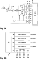
- Figure 1A shows an exemplary embodiment for the basic structure of a transmission arrangement S for connection to a D [display] S [erial] I [nterface] data transmission interface IS or also to a C [amera] S [erial] I [nterface] data transmission interface IS.
- the image data generated in the application processor AP or in the camera KA are transmitted on four data lines or channels CH0 +, CH0-, CH1 +, CH1-, CH2 +, CH2-, CH3 +, CH3- as D-PHY signals at the data transmission interface, which is up to four bits wide IS provided together with D-PHY-correct clock signals CLK +, CLK-.
- the transmission arrangement S receives these signals on an integrated interface logic LS, whose blocks each have at least one state machine for correct interpretation of the D-PHY logic signals and for differentiating between high-frequency data streams (so-called H [igh] S [peed] data) and low-frequency data streams (so-called L [ow] S [peed] data) can have.
- a framer FR following in the transmission arrangement S ensures the D [irect] C [urrent] balancing of the input signal and generates a signal on the receiving side (cf. Figure 2A ) recognizable frame, which the receiving arrangement E (cf. Figure 2A ) enables the received data to be reassigned to the correct output data lines or output channels CH0 +, CH0-, CH1 +, CH1-, CH2 +, CH2-, CH3 +, CH3-.
- the framer FR can according to Figure 1B both the single-ended data signals HSD0, HSD1, HSD2, HSD3 based on logic levels and the differential data signals DD0 +, DD0-, DD1 +, DD1-, DD2 +, DD2-, DD3 +, DD3- can be applied.
- the framer embeds FR in accordance with Figure 1B these differential data signals DD0 +, DD0-, DD1 +, DD1-, DD2 +, DD2-, DD3 +, DD3- in the stream of the single-ended, logic level-based data signals HSD0, HSD1, HSD2, HSD3.
- the framer FR and the multiplexer MU together form the serializer SE.
- the D-PHY clock signal provided via the clock port CLK +, CLK- and via the clock module CS of the interface logic LS by means of the clock generator PS serves as a (clock) reference for the serializer SE, in particular for its multiplexer MU, and is embedded in the serial data stream, i.e. in the serialized output signal. This creates the common signal current SI, which is sent to the receiving arrangement E (cf. Figure 2A ) is transmitted.
- the output driver AT is an integrated laser driver for controlling at least one directly connected laser LA, in particular for controlling at least one directly connected laser V [ertical] C [avity] S [urface] E [mitting] L [aserdiode].
- Figure 2A shows an exemplary embodiment for the basic structure of a receiving arrangement E for connection to a D [display] S [serial] I [nterface] data transmission interface IE or also to a C [amera] S [erial] I [nterface] data transmission interface IE.
- the transmission arrangement S (cf. Figure 1A ) sent serial or bundled data are received via an input amplifier EV of the receiving arrangement E and fed to an integrated clock and data recovery CD.
- This integrated clock and data recovery CD regenerates the original D-PHY clock from the common signal stream SI, which is transmitted directly to the D [display] S [erial] I [nterface] or the C [amera] via the clock module CE of the interface logic LE ] S [erial] I [nterface] will be made available again.
- the remaining serial data stream is unbundled and parallelized via a demultiplexer DM and sent to a deframer DF (cf. Figure 2B ), which is basically the mirror image of the framer FR in accordance with Figure 1B is constructed.
- the demultiplexer DM and the deframer DF together form the deserializer DS.
- the Deframer FR can according to Figure 2B the differential data signals DD0 +, DD0-, DD1 +, DD1-, DD2 +, DD2-, DD3 +, DD3- from the single-ended data signals HSD0, HSD1, HSD2, HSD3 based on logic levels by means of its decoder DK designed as a 6b / 5b decoder block separate and reassign the repaired data signals to the respectively applicable data lines CH0 +, CH0-, CH1 +, CH1-, CH2 +, CH2-, CH3 +, CH3-.
- the interface logic blocks LE shown in the receiving arrangement E can each have at least one state machine for correctly interpreting the D-PHY logic signals and for differentiating between high-frequency data streams and low-frequency data streams.
- the input amplifier EV is designed as an integrated transimpedance amplifier, which makes it possible to connect a photodiode FD directly to the receiving arrangement E.
- the cable-based multiplexed connection between the transmission arrangement S (cf. Figure 1A ) and the receiving arrangement E (cf. Figure 2A ) on an optical basis namely by means of an optical waveguide OM designed, for example, in the form of a glass fiber and / or in the form of a plastic fiber, and to operate it.
Description
Die vorliegende Erfindung betrifft eine Schaltungsanordnung gemäß dem Oberbegriff des Anspruchs 1 sowie ein Verfahren gemäß dem Oberbegriff des Anspruchs 11.The present invention relates to a circuit arrangement according to the preamble of claim 1 and a method according to the preamble of claim 11.
Die Bitübertragungsschicht oder physikalische Schicht (PHY) ist die unterste Schicht im O[pen]S[ystems]I[nterconnection]-Schichtenmodell, das auch OSI-Referenzmodell genannt wird und ein Schichtenmodell der Internationalen Organisation für Normung (ISO) bezeichnet, das wiederum als Designgrundlage von Kommunikationsprotokollen in Rechnernetzen dient.The bit transmission layer or physical layer (PHY) is the lowest layer in the O [pen] S [ystems] I [nterconnection] layer model, which is also called the OSI reference model and a layer model of the International Organization for Standardization (ISO), which in turn serves as a design basis for communication protocols in computer networks.
Die Physical Layer (PHY) ist für Combining, F[orward]E[rror]C[orrection], Modulation, Power Control, Spreading (C[ode]D[ivision]M[ultiple]A[ccess]) und dergleichen zuständig und kennt weder Daten noch Anwendungen, sondern nur Nullen und Einsen. PHY stellt der darüber liegenden Sicherungsschicht (D[ata]L[ink]L[ayer]), insbesondere einer Teilschicht namens M[edia]A[ccess]C[ontrol]-Layer, logische Kanäle zur Verfügung (Transportkanäle bei U[niversal]M[obile]T[elecommunications]S[ystem]).The physical layer (PHY) is responsible for combining, forward] e [rror] correction], modulation, power control, spreading (C [ode] D [ivision] M [ultiple] A [ccess]) and the like and knows neither data nor applications, only zeros and ones. PHY provides the overlying security layer (D [ata] L [ink] L [ayer]), in particular a sublayer called M [edia] A [ccess] C [ontrol] layer, logical channels (transport channels in the case of Universal ] M [obile] T [elecommunications] S [ystem]).
D-PHY ermöglicht grundsätzlich eine flexible, kostengünstige und schnelle serielle Schnittstelle für Kommunikationsverbindungen zwischen Komponenten innerhalb einer mobilen Vorrichtung.D-PHY basically enables a flexible, inexpensive and fast serial interface for communication connections between components within a mobile device.
Wie anhand
Ein auf dem D-PHY-Protokoll basierendes DSI oder DSI-2 oder CSI oder CSI-2 oder CSI-3 umfasst bis zu vier differentielle Datenleitungen und eine differentielle Taktleitung, die den Applikationsprozessor elektrisch mittels Kupferkabel mit dem Display und/oder mit der Kamera verbinden. Die Datenrate pro differentieller Datenleitung beträgt bis zu 1,5 Gbps (Gigabit pro Sekunde).A DSI or DSI-2 or CSI or CSI-2 or CSI-3 based on the D-PHY protocol comprises up to four differential data lines and a differential clock line that electrically connects the application processor to the display and / or the camera using copper cables connect. The data rate per differential data line is up to 1.5 Gbps (gigabits per second).
Dieses konventionelle Versenden und Empfangen der D-PHY-DSI- oder D-PHY-CSI-Signale über ein bis vier differentielle Datensignale und eine differentielle Taktleitung ist in der D-PHY-Schnittstellenkonfiguration der
Wie in diesem Zusammenhang aus
Mit zunehmender Auflösung von Displays und Kameras steigen auch die Datenraten vom Applikationsprozessor zum Display bzw. von der Kamera zum Applikationsprozessor. Die hierbei während der Datenübertragung erzeugten hochfrequenten elektromagnetischen Felder stören die empfindlichen benachbarten Empfänger von hochfrequenten Nutzsignalen, wie zum Beispiel den Bluetooth-, G[lobal]P[ositioning]S[ystem]-, U[niversal]M[obile]T[elecommunications]S[ystem]- oder Wi-Fi-Empfänger, und beeinträchtigen damit deren Funktion erheblich.As the resolution of displays and cameras increases, so do the data rates from the application processor to the display or from the camera to the application processor. The high-frequency electromagnetic fields generated during the data transmission interfere with the sensitive neighboring receivers of high-frequency useful signals, such as the Bluetooth, G [lobal] P [ositioning] S [system], U [niversal] M [obile] T [telecommunications] ] S [ystem] or Wi-Fi receivers, and thus significantly impair their function.
Umfangreiche und somit kostenaufwändige Abschirmmaßnahmen an den Übertragungskabeln sind notwendig, um einen störungsfreien Betrieb der vorgenannten Empfänger sicherzustellen.Extensive and therefore costly shielding measures on the transmission cables are necessary in order to ensure trouble-free operation of the aforementioned receivers.
Mit zunehmender Anzahl an Displays und an Kameras in modernen Mobiltelefonen oder vergleichbaren Geräten können die Kabelbaumgrößen in derartigen Geräten leicht auf bis zu sechzig Leitungen ansteigen, die nur für die Übertragung von Bilddaten benötigt werden. Diese Kabelbaumgrößen verhindern nachteiligerweise eine weitere Miniaturisierung derartiger Geräte.With an increasing number of displays and cameras in modern cell phones or comparable devices, the cable harness sizes in such devices can easily increase to up to sixty lines that are only required for the transmission of image data. These wire harness sizes disadvantageously prevent further miniaturization of such devices.
In der vom 3. März 2011 datierenden Informationsschrift "
Ausgehend von den vorstehend dargelegten Nachteilen und Unzulänglichkeiten sowie unter Würdigung des umrissenen Standes der Technik liegt der vorliegenden Erfindung die Aufgabe zugrunde, eine Schaltungsanordnung der eingangs genannten Art sowie ein Verfahren der eingangs genannten Art so weiterzuentwickeln, dass eine weitereOn the basis of the disadvantages and inadequacies set out above and taking into account the prior art outlined, the object of the present invention is to further develop a circuit arrangement of the type mentioned and a method of the type mentioned so that a further
Miniaturisierung von Gerätschaften, denen eine derartige Schaltungsanordnung sowie ein derartiges Verfahren zugeordnet sind, ermöglicht wird.Miniaturization of equipment to which such a circuit arrangement and such a method are assigned is made possible.
Diese Aufgabe wird durch eine Schaltungsanordnung mit den Merkmalen des Anspruchs 1 sowie durch ein Verfahren mit den Merkmalen des Anspruchs 11 gelöst. Vorteilhafte Ausgestaltungen und zweckmäßige Weiterbildungen der vorliegenden Erfindung sind in den jeweiligen Unteransprüchen gekennzeichnet.This object is achieved by a circuit arrangement having the features of claim 1 and by a method having the features of claim 11. Advantageous configurations and expedient developments of the present invention are characterized in the respective subclaims.
Erfindungsgemäß wird also zum einen eine Sendeanordnung vorgeschlagen, mittels derer
- die single-ended, auf Logikpegeln basierenden Signalen entsprechenden H[igh]S[peed]-Daten und
- die differentiellen, auf common mode basierenden, Signalen entsprechenden L[ow]P[ower]-Daten
- the single-ended signals based on logic levels corresponding to H [igh] S [peed] data and
- L [ow] P [ower] data corresponding to differential signals based on common mode
Des Weiteren wird erfindungsgemäß eine Empfangsanordnung vorgeschlagen, mittels derer dieser gemeinsame Signalstrom wieder
- in die single-ended, auf Logikpegeln basierenden Signalen entsprechenden H[igh]S[peed]-Daten und
- die differentiellen, auf common mode basierenden, Signalen entsprechenden L[ow]P[ower]-Daten
- into the single-ended logic level-based signals corresponding to H [igh] S [peed] data and
- L [ow] P [ower] data corresponding to differential signals based on common mode
Hierbei können die verschiedenen Signale für den zwischen der Sendeanordnung und der Empfangsanordnung erfolgenden Transport über mindestens ein optisches Medium, insbesondere über mindestens einen optischen Wellenleiter, zum Beispiel über mindestens eine Glasfaser und/oder über mindestens eine Plastikfaser, zum gemeinsamen Signalstrom aufbereitet, insbesondere sendeseitig gebündelt oder serialisiert und empfangsseitig entbündelt oder deserialisiert, werden.Here, the various signals for the transport taking place between the transmitting arrangement and the receiving arrangement via at least one optical medium, in particular via at least one optical waveguide, for example via at least one glass fiber and / or via at least one plastic fiber, can be processed into a common signal stream, in particular bundled on the transmission side or serialized and unbundled or deserialized at the receiving end.
In einer bevorzugten Weiterbildung der vorliegenden Erfindung können unter Berücksichtigung der Besonderheiten des D-PHY-Protokolls auf Seiten der Sendeanordnung mindestens eine, insbesondere bis zu vier, differentielle Datenleitungen und mindestens eine, insbesondere genau eine, differentielle Taktleitung des D[isplay]S[erial]I[nterface], auch in der Spezifikation DSI-2, und/oder des C[amera]S[erial]I[nterface], auch in den Spezifikationen CSI-2 und/oder CSI-3, serialisiert werden, insbesondere durch Serialisieren der differentiellen Datenleitungen und der differentiellen Taktleitung des D[isplay]S[erial]I[nterface] und/oder des C[amera]S[erial]I[nterface].In a preferred development of the present invention, taking into account the special features of the D-PHY protocol, at least one, in particular up to four, differential data lines and at least one, in particular exactly one, differential clock line of the display serial ] I [nterface], also in the specification DSI-2, and / or the C [amera] S [erial] I [nterface], also in the specifications CSI-2 and / or CSI-3, in particular by Serializing the differential data lines and the differential clock line of the D [isplay] S [erial] I [nterface] and / or the C [amera] S [erial] I [nterface].
In entsprechend bevorzugter Weiterbildung der vorliegenden Erfindung kann unter Berücksichtigung der Besonderheiten des D-PHY-Protokolls ein gemäß vorstehend dargelegter Sendeanordnung gebündelter oder serialisierter gemeinsamer Signalstrom auf Seiten der Empfangsanordnung aufgenommen werden, um daraus die mindestens eine, insbesondere die bis zu vier, differentiellen Datenleitungen und die mindestens eine, insbesondere die genau eine, differentielle Taktleitung für das DSI, auch in der Spezifikation DSI-2, und/oder für das CSI, auch in den Spezifikationen CSI-2 und/oder CSI-3, zurückzugewinnen, insbesondere durch Entbündeln.In a correspondingly preferred development of the present invention, taking into account the peculiarities of the D-PHY protocol, a common signal stream bundled or serialized according to the transmission arrangement set out above can be recorded on the side of the receiving arrangement in order to use it to generate the at least one, in particular the up to four, differential data lines and to recover the at least one, in particular exactly one, differential clock line for the DSI, also in the DSI-2 specification, and / or for the CSI, also in the CSI-2 and / or CSI-3 specifications, in particular by unbundling.
Im Ergebnis bietet die vorliegende Erfindung eine Möglichkeit,
- single-ended, auf Logikpegeln basierende Daten- und Taktsignale und
- differentielle, insbesondere auf common mode basierende, Daten- und Taktsignale gemeinsam optisch zu übertragen, insbesondere in der Ausgestaltung als D-PHY-Signale, und hierbei zum Beispiel in der Ausgestaltung als MIPI-D-PHY-Signale.
- single-ended data and clock signals based on logic levels and
- to optically transmit differential, in particular based on common mode, data and clock signals together, in particular in the form of D-PHY signals, and here for example in the form of MIPI-D-PHY signals.
Durch die optische Übertragung werden keine hochfrequenten elektromagnetischen Felder erzeugt, die empfindliche benachbarte Empfänger von hochfrequenten Nutzsignalen, wie zum Beispiel Bluetooth-, G[lobal]P[ositioning]S[ystem]-, U[niversal]M[obile]T[elecommunications]S[ystem]- oder Wi-Fi-Empfänger stören könnten. Damit wird deren Funktion auch nicht beeinträchtigt.The optical transmission does not generate any high-frequency electromagnetic fields that could affect sensitive neighboring receivers of high-frequency useful signals such as Bluetooth, global positioning, universal, mobile telecommunications ] S [ystem] or Wi-Fi receivers. This also does not impair their function.
Vorteilhafterweise entfallen also umfangreiche, kostenaufwändige Abschirmungsmaßnahmen an den Übertragungsmedien. Die Anzahl an Übertragungskanälen kann auf einen optischen Wellenleiter pro Display und/oder pro Kamera reduziert werden.Advantageously, extensive, costly shielding measures on the transmission media are not required. The number of transmission channels can be reduced to one optical waveguide per display and / or per camera.
Exemplarisch lässt sich die vorliegende Erfindung beim gleichzeitigen seriellen und/oder gebündelten, insbesondere CSI-protokollbasierten und/oder CSI-2-protokollbasierten und/oder CSI-3-protokollbasierten und/oder DSI-protokollbasierten und/oder DSI-2-protokollbasierten, Übertragen sowohl von single-ended, auf Logikpegeln basierenden Daten- und Taktsignalen als auch von differentiellen, insbesondere auf common mode basierenden, Daten- und Taktsignalen, insbesondere von D-PHY-Datensignalen und D-PHY-Taktsignalen, zum Beispiel von bis zu vier Bit breiten MIPI-D-PHY-Datensignalen und MIPI-D-PHY-Taktsignalen, zwischen mindestens einer Datenquelle, insbesondere mindestens einer, zum Beispiel hochauflösenden und/oder zum Beispiel als Bildquelle fungierenden, Kamera und/oder mindestens einem Applikationsprozessor, und mindestens einer Datensenke, insbesondere mindestens einem Applikationsprozessor und/oder mindestens einer, zum Beispiel hochauflösenden und/oder zum Beispiel als Bildsenke fungierenden, Anzeigeeinheit, zum Beispiel mindestens einem Display oder mindestens einem Monitor, anwenden.As an example, the present invention can be transmitted with simultaneous serial and / or bundled, in particular CSI-protocol-based and / or CSI-2-protocol-based and / or CSI-3-protocol-based and / or DSI-protocol-based and / or DSI-2-protocol-based, transmission both single-ended data and clock signals based on logic levels and differential data and clock signals, in particular data and clock signals based on common mode, in particular D-PHY data signals and D-PHY clock signals, for example of up to four bits wide MIPI-D-PHY data signals and MIPI-D-PHY clock signals, between at least one data source, in particular at least one, for example high-resolution and / or for example functioning as an image source, Camera and / or at least one application processor, and at least one data sink, in particular at least one application processor and / or at least one, for example high-resolution and / or for example acting as an image sink, display unit, for example at least one display or at least one monitor.
Wie bereits vorstehend erörtert, gibt es verschiedene Möglichkeiten, die Lehre der vorliegenden Erfindung in vorteilhafter Weise auszugestalten und weiterzubilden. Hierzu wird einerseits auf die dem Anspruch 1 sowie dem Anspruch 11 nachgeordneten Ansprüche verwiesen, andererseits werden weitere Ausgestaltungen, Merkmale und Vorteile der vorliegenden Erfindung nachstehend unter Anderem anhand der durch
Es zeigt:
- Fig. 1A
- in konzeptuell-schematischer Darstellung ein Ausführungsbeispiel des ersten Teils, nämlich der gemäß der vorliegenden Erfindung ausgebildeten Sendeanordnung einer Schaltungsanordnung, die nach dem Verfahren gemäß der vorliegenden Erfindung arbeitet;
- Fig. 1B
- in konzeptuell-schematischer Detaildarstellung ein Ausführungsbeispiel des Framers der Sendeanordnung aus
Fig. 1A ; - Fig. 2A
- in konzeptuell-schematischer Darstellung ein Ausführungsbeispiel des zweiten Teils, nämlich der gemäß der vorliegenden Erfindung ausgebildeten Empfangsanordnung einer Schaltungsanordnung, die nach dem Verfahren gemäß der vorliegenden Erfindung arbeitet;
- Fig. 2B
- in konzeptuell-schematischer Detaildarstellung ein Ausführungsbeispiel des Deframers der Empfangsanordnung aus
Fig. 2A ; - Fig. 3A
- in konzeptuell-schematischer Darstellung ein Beispiel einer Anordnung aus dem Stand der Technik; und
- Fig. 3B
- in konzeptuell-schematischer Darstellung ein Beispiel einer der Anordnung aus
- Fig. 3A
- zugrunde liegenden Schnittstellenkonfiguration mit zwei Datenkanälen und mit einer Taktleitung.
- Figure 1A
- in a conceptual-schematic representation an exemplary embodiment of the first part, namely the transmission arrangement of a circuit arrangement designed according to the present invention that operates according to the method according to the present invention;
- Figure 1B
- in a conceptual-schematic detailed representation of an embodiment of the framer of the transmission arrangement
Figure 1A ; - Figure 2A
- in a conceptual-schematic representation an embodiment of the second part, namely the receiving arrangement of a circuit arrangement which is designed according to the present invention and which operates according to the method according to the present invention;
- Figure 2B
- in a conceptual-schematic detailed representation an embodiment of the deframer of the receiving arrangement
Figure 2A ; - Figure 3A
- in a conceptual-schematic representation an example of an arrangement from the prior art; and
- Figure 3B
- in a conceptual-schematic representation an example of one of the arrangements
- Figure 3A
- underlying interface configuration with two data channels and one clock line.
Gleiche oder ähnliche Ausgestaltungen, Elemente oder Merkmale sind in
- Mittels des anhand
Fig. 1A veranschaulichten Ausführungsbeispiels einer Sendeanordnung S gemäß der vorliegenden Erfindung und - mittels des anhand
Fig. 2A veranschaulichten Ausführungsbeispiels einer Empfangsanordnung E gemäß der vorliegenden Erfindung,
durch die zusammen ein Ausführungsbeispiel einer Schaltungsanordnung S, E (vgl.Fig. 1A ,Fig. 2A ) gemäß der vorliegenden Erfindung gebildet wird (im Rahmen der vorliegenden Erfindung ist es möglich, die Sendeanordnung S und die Empfangsanordnung E unabhängig voneinander zu realisieren und zu betreiben), ist es grundsätzlich möglich, eine kabelbasierte Verbindung - gemultiplext und mithin serialisiert auf optischer Basis, insbesondere auf Basis mindestens eines optischen Mediums, zum Beispiel auf Basis mindestens eines optischen Wellenleiters OM (vgl. hierzu im Detail
Fig. 1A ,Fig. 2A ), wie etwa auf Basis mindestens einer Glasfaser und/oder auf Basis mindestens einer Plastikfaser, und/oder - nicht gemultiplext auf elektrischer oder galvanischer Basis, insbesondere auf Basis mindestens einer elektrischen oder galvanischen Verbindung, zum Beispiel auf Basis mindestens eines Kupferkabels und/oder auf Basis mindestens einer, etwa auf mindestens einer Leiterplatte angeordneten, elektrischen Leitung,
- Using the based
Figure 1A illustrated embodiment of a transmission arrangement S according to the present invention and - by means of the
Figure 2A illustrated embodiment of a receiving arrangement E according to the present invention,
through which together an exemplary embodiment of a circuit arrangement S, E (cf.Figure 1A ,Figure 2A ) is formed according to the present invention (within the scope of the present invention it is possible to implement and operate the transmitting arrangement S and the receiving arrangement E independently of one another), it is basically possible to use a cable-based connection - multiplexed and therefore serialized on an optical basis, in particular on the basis of at least one optical medium, for example on the basis of at least one optical waveguide OM (cf. in this regard in detail
Figure 1A ,Figure 2A ), such as based on at least one glass fiber and / or based on at least one plastic fiber, and / or - non-multiplexed on an electrical or galvanic basis, in particular on the basis of at least one electrical or galvanic connection, for example on the basis of at least one copper cable and / or on the basis of at least one electrical line arranged on at least one printed circuit board, for example,
Die im Applikationsprozessor AP oder in der Kamera KA generierten Bilddaten werden auf vier Datenleitungen oder Kanälen CH0+, CH0-, CH1+, CH1-, CH2+, CH2-, CH3+, CH3- als D-PHY-Signale an der bis zu vier Bit breiten Datenübertragungsschnittstelle IS zusammen mit D-PHY-korrekten Taktsignalen CLK+, CLK- zur Verfügung gestellt.The image data generated in the application processor AP or in the camera KA are transmitted on four data lines or channels CH0 +, CH0-, CH1 +, CH1-, CH2 +, CH2-, CH3 +, CH3- as D-PHY signals at the data transmission interface, which is up to four bits wide IS provided together with D-PHY-correct clock signals CLK +, CLK-.
Die Sendeanordnung S nimmt diese Signale an einer integrierten Interface-Logik LS auf, deren Blöcke jeweils mindestens einen Zustandsautomaten zur richtigen Interpretation der D-PHY-Logiksignale und zur Unterscheidung zwischen hochfrequenten Datenströmen (sogenannten H[igh]S[peed]-Daten) und niederfrequenten Datenströmen (sogenannten L[ow]S[peed]-Daten) aufweisen können.The transmission arrangement S receives these signals on an integrated interface logic LS, whose blocks each have at least one state machine for correct interpretation of the D-PHY logic signals and for differentiating between high-frequency data streams (so-called H [igh] S [peed] data) and low-frequency data streams (so-called L [ow] S [peed] data) can have.
Ein in der Sendeanordnung S folgender Framer FR (vgl. hierzu detaillierter
Im Detail kann der Framer FR gemäß
Ein sich dem Framer FR anschließender Multiplexer MU, insbesondere H[igh]S[peed]-Mux, erzeugt mit Hilfe eines als Phase-Locked-Loop, insbesondere als C[lock]M[ultiplier]U[nit], ausgebildeten Taktgenerators PS das hochfrequente serielle oder gebündelte Sendesignal, das dem Ausgang AS der Sendeanordnung S mittels eines Ausgangstreiber AT zur Verfügung gestellt wird. Der Framer FR und der Multiplexer MU bilden zusammen den Serialisierer SE.A multiplexer MU connected to the framer FR, in particular H [igh] S [peed] -Mux, generates clock generator PS designed as a phase-locked loop, in particular as C [lock] multiplier] U [nit] the high-frequency serial or bundled transmission signal which is made available to the output AS of the transmission arrangement S by means of an output driver AT. The framer FR and the multiplexer MU together form the serializer SE.
Hierbei dient das über den Taktport CLK+, CLK- und über das Taktmodul CS der Interface-Logik LS mittels des Taktgenerators PS bereit gestellte D-PHY-Taktsignal als (Takt-)Referenz für den Serialisierer SE, insbesondere für dessen Multiplexer MU, und wird im seriellen Datenstrom, also im serialisierten Ausgangssignal eingebettet. Hierdurch entsteht der gemeinsame Signalstrom SI, der an die Empfangsanordnung E (vgl.
Wie der Darstellung gemäß
Die von der Sendeanordnung S (vgl.
Diese integrierte Takt- und Datenrückgewinnung CD regeneriert aus dem gemeinsamen Signalstrom SI den ursprünglichen D-PHY-Takt, der über das Taktmodul CE der Interface-Logik LE direkt dem D[isplay]S[erial]I[nterface] oder dem C[amera]S[erial]I[nterface] wieder zur Verfügung gestellt wird. Der verbleibende serielle Datenstrom wird über einen Demultiplexer DM entbündelt sowie parallelisiert und an einen Deframer DF (vgl. hierzu detaillierter
Im Detail kann der Deframer FR gemäß
Die in der Empfangsanordnung E dargestellten Interface-Logik-Blöcke LE können jeweils mindestens einen Zustandsautomaten zur richtigen Interpretation der D-PHY-Logiksignale und zur Unterscheidung zwischen hochfrequenten Datenströmen und niederfrequenten Datenströmen aufweisen.The interface logic blocks LE shown in the receiving arrangement E can each have at least one state machine for correctly interpreting the D-PHY logic signals and for differentiating between high-frequency data streams and low-frequency data streams.
Wie der Darstellung gemäß
Auf diese Weise ist es bei der Schaltungsanordnung S, E (vgl.
- EE.
- EmpfangsanordnungReceiving arrangement
- SS.
- SendeanordnungSend arrangement
- AEAE
- Ausgang der Empfangsanordnung EOutput of the receiving arrangement E
- APAP
- ApplikationsprozessorApplication processor
- ASAS
- Ausgang der Sendeanordnung SOutput of the transmission arrangement S
- ATAT
- Ausgangstreiber, insbesondere LasertreiberOutput drivers, especially laser drivers
- CDCD
- Takt- und DatenrückgewinnungseinheitClock and data recovery unit
- CECE
- Taktmodul der Empfangs-Schnittstellen-Logik LEClock module of the receiving interface logic LE
- CH0±CH0 ±
- erste Datenleitung oder erster Kanalfirst data line or first channel
- CH1±CH1 ±
- zweite Datenleitung oder zweiter Kanalsecond data line or second channel
- CH2±CH2 ±
- dritte Datenleitung oder dritter Kanalthird data line or third channel
- CH3±CH3 ±
- vierte Datenleitung oder vierter Kanalfourth data line or fourth channel
- CLK±CLK ±
- Taktleitung oder TaktkanalClock line or clock channel
- CSCS
- Taktmodul der Sende-Schnittstellen-Logik LSClock module of the transmission interface logic LS
- DD0±DD0 ±
- differentielles, insbesondere auf common mode basierendes, Datensignal auf erster Datenleitung oder erstem Kanal CH0±differential data signal, in particular based on common mode, on first data line or first channel CH0 ±
- DD1±DD1 ±
- differentielles, insbesondere auf common mode basierendes, Datensignal auf zweiter Datenleitung oder zweitem Kanal CH1±differential data signal, in particular based on common mode, on second data line or second channel CH1 ±
- DD2±DD2 ±
- differentielles, insbesondere auf common mode basierendes, Datensignal auf dritter Datenleitung oder drittem Kanal CH2±differential data signal, in particular based on common mode, on third data line or third channel CH2 ±
- DD3±DD3 ±
- differentielles, insbesondere auf common mode basierendes, Datensignal auf vierter Datenleitung oder viertem Kanal CH3±differential data signal, in particular based on common mode, on fourth data line or fourth channel CH3 ±
- DFDF
- DeframerDeframer
- DKDK
- Dekodierer, insbesondere 6b/5b-Dekodierblock, des Deframers DFDecoder, in particular 6b / 5b decoder block, of the deframer DF
- DMDM
- DemultiplexerDemultiplexer
- DSDS
- Deserialisierungselement oder DeserialisiererDeserializer or deserializer
- DUYOU
- AnzeigeeinheitDisplay unit
- EEEE
- Eingang der Empfangsanordnung EInput of the receiving arrangement E
- ESIT
- Eingang der Sendeanordnung SInput of the transmission arrangement S
- EVEV
- Eingangsverstärker, insbesondere TransimpedanzverstärkerInput amplifiers, especially transimpedance amplifiers
- FDFD
- FotodiodePhotodiode
- FRFR
- FramerFramer
- HSD0HSD0
- single-ended, auf Logikpegeln basierendes Datensignal auf erster Datenleitung oder erstem Kanal CH0±single-ended data signal based on logic levels on first data line or first channel CH0 ±
- HSD1HSD1
- single-ended, auf Logikpegeln basierendes Datensignal auf zweiter Datenleitung oder zweitem Kanal CH1±single-ended data signal based on logic levels on second data line or second channel CH1 ±
- HSD2HSD2
- single-ended, auf Logikpegeln basierendes Datensignal auf dritter Datenleitung oder drittem Kanal CH2±single-ended data signal based on logic levels on third data line or third channel CH2 ±
- HSD3HSD3
- single-ended, auf Logikpegeln basierendes Datensignal auf vierter Datenleitung oder viertem Kanal CH3±single-ended data signal based on logic levels on fourth data line or fourth channel CH3 ±
- IEIE
- datensenkenbezogene CSI- und/oder CSI-2- und/oder CSI-3- und/oder DSI- und/oder DSI-2-Schnittstelledata sink related CSI and / or CSI-2 and / or CSI-3 and / or DSI and / or DSI-2 interface
- ISIS
- datenquellenbezogene CSI- und/oder CSI-2- und/oder CSI-3- und/oder DSI- und/oder DSI-2-Schnittstelledata source-related CSI and / or CSI-2 and / or CSI-3 and / or DSI and / or DSI-2 interface
- KAKA
- Kameracamera
- KOKO
- Kodierer, insbesondere 5b/6b-Kodierblock, des Framers FREncoder, in particular 5b / 6b coding block, of the framer FR
- LALA
- Laserlaser
- LELE
- Empfangs-Schnittstellen-LogikReceive interface logic
- LSLS
- Sende-Schnittstellen-LogikSend interface logic
- MUMU
- Multiplexermultiplexer
- OMOM
- optisches Medium, insbesondere optischer Wellenleiter, zum Beispiel Glasfaser und/oder Plastikfaseroptical medium, in particular optical waveguides, for example glass fiber and / or plastic fiber
- PSPS
- Taktgenerator, insbesondere Phase-Locked-Loop, zum Beispiel Clock Multiplier UnitClock generator, in particular phase-locked loop, for example clock multiplier unit
- SESE
- Serialisierungselement oder SerialisiererSerializer or serializer
- SISI
- gemeinsamer Signalstromcommon signal stream
- TLTL
- TaktleitungClock line
Claims (15)
- A circuit arrangement (S, E) for transmitting- single-ended logic-level-based data signals and clock signals (HS) as well as- differential common-mode-based data signals and clock signals (LP)in the form of at least one serialized common signal stream (SI) between at least one sending arrangement (S) assignable to at least one data source and at least one receiving arrangement (E) assignable to at least one data sink, said common signal stream (SI) being serialized by means of at least one serializer (SE) assigned to the sending arrangement (S), wherein the data rate of the differential data signals and clock signals (LP) is different from the data rate of the single-ended logic-level-based data signals and clock signals (HS),
characterized by
at least one multiplexer (MU) assigned to the serializer (SE), said multiplexer (MU) for generating the common signal stream (SI), said multiplexer (MU) comprising:- at least one filter (FI) for differentiating the differential data signals and/or clock signals (LP) from the single-ended logic-level-based data signals and/or clock signals (HS), and- at least one further multiplexer (MUZ) providable additionally with the differential data signals and/or clock signals (LP) coming from the filter (FI). - The circuit arrangement according to claim 1, characterized in that the data rate of the differential data signals and clock signals (LP) is smaller than the data rate of the single-ended logic-level-based data signals and clock signals (HS).
- The circuit arrangement according to claim 1 or 2, characterized in that the sending arrangement (S) comprises:- at least one input (ES) for the data signals and clock signals (HS; LP),- at least one sending interface logic (LS) connected downstream of the input (ES) for picking up the data signals and clock signals (HS, LP),- the at least one serializer (SE) connected downstream of the sending interface logic (LS) for generating the common signal stream (SI),- at least one clock generator (PS) connected downstream of at least one clock module (CS) of the sending interface logic (LS), connected upstream of the serializer (SE) and provided for generating at least one reference clock,- at least one output driver (AT) connected downstream of the serializer (SE), and- at least one output (AS) connected downstream of the output driver (AT) for transmitting the common signal stream (SI) to the receiving arrangement (E).
- The circuit arrangement according to claim 3, characterized in that the clock generator (PS) is embodied as at least one phase-locked loop, in particular as at least one clock multiplier unit.
- The circuit arrangement according to claim 3 or 4, characterized in that the serializer (SE) comprises:- at least one framer (FR) connected downstream of the sending interface logic (LS) for generating at least one frame recognizable in the receiving arrangement (E) for the common signal stream (SI) as well as- the at least one multiplexer (MU) connected downstream of the framer (FR) for generating the common signal stream (SI).
- The circuit arrangement according to claim 5, characterized in that the framer (FR) is providable with the single-ended logic-level-based data signals (HSDO, HSD1, HSD2, HSD3) as well as with the differential data signals (DD0+, DD0-, DD1+, DD1-, DD2+, DD2-, DD3+, DD3-) and that the framer (FR), by means of at least one coder (KO), in particular by means of at least one 5b/6b coder block, embeds the differential data signals (DD0+, DD0-, DD1+, DD1-, DD2+, DD2-, DD3+, DD3-) in the stream of the single-ended logic-level-based data signals (HSDO, HSD1, HSD2, HSD3).
- The circuit arrangement according to at least one of claims 1 to 6, characterized in that the receiving arrangement (E) comprises:- at least one input (EE) for the common signal stream (SI) transmitted by the sending arrangement (S),- at least one input amplifier (EV) for picking up the common signal stream (SI),- at least one clock and data recovery unit (CD) for recovering the data signals and clock signals (HS, LP) from the common signal stream (SI),- at least one clock module (CE) of at least one receiving interface logic (LE), said clock module (CE) connected downstream of the clock and data recovery unit (CD),- at least one deserializer (DS) connected downstream of the clock and data recovery unit (CD) for re-parallelizing the data signals and/or clock signals (HS, LP) and for assigning the re-parallelized data signals and/or clock signals (HS, LP) to the receiving interface logic (LE), and- at least one output (AE) connected downstream of the receiving interface logic (LE) for the data signals and clock signals (HS, LP).
- The circuit arrangement according to claim 7, characterized in that the deserializer (DS) comprises:- at least one demultiplexer (DM) connected downstream of the clock and data recovery unit (CD) for re-parallelizing the data signals and/or clock signals (HS, LP) as well as- at least one deframer (DF) connected downstream of the demultiplexer (DM) for assigning the re-parallelized data signals and/or clock signals (HS, LP) to the receiving interface logic (LE).
- The circuit arrangement according to claim 8, characterized in that the deframer (DF) separates the differential data signals (DD0+, DD0-, DD1+, DD1-, DD2+, DD2-, DD3+, DD3-) from the single-ended logic-level-based data signals (HSDO, HSD1, HSD2, HSD3) by means of at least one decoder (DK), in particular by means of at least one 6b/5b decoder block, and that the deframer (DF) assigns the re-parallelized data signals to the respective data lines (CH0+, CH0-, CH1+, CH1-, CH2+, CH2-, CH3+, CH3-).
- The circuit arrangement according to at least one of claims 1 to 9, characterized in that the common signal stream (SI) is transmittable between the sending arrangement (S) and the receiving arrangement (E)- via at least one optical medium (OM), in particular via at least one optical waveguide, for example via at least one glass fibre and/or via at least one plastic fibre, and/or- via at least one electrical or galvanic link (GA), in particular of one bit width, in particular via at least one copper cable and/or via at least one electrical line, for example provided on at least one printed circuit board.
- A method for transmitting- single-ended logic-level-based data signals and clock signals (HS) as well as- differential common-mode-based data signals and clock signals (LP)in the form of at least one serialized common signal stream (SI) between at least one sending arrangement (S) assignable to at least one data source and at least one receiving arrangement (E) assignable to at least one data sink, said common signal stream (SI) being serialized by means of at least one serializer (SE), wherein the data rate of the differential data signals and clock signals (LP) is different from the data rate of the single-ended logic-level-based data signals and clock signals (HS)
characterized by
at least one multiplexer (MU) assigned to the serializer (SE), said multiplexer (MU) for generating the common signal stream (SI), said multiplexer (MU) comprising:- at least one filter (FI) for differentiating the differential data signals and/or clock signals (LP) from the single-ended logic-level-based data signals and/or clock signals (HS), and- at least one further multiplexer (MUZ) provided additionally with the differential data signals and/or clock signals (LP) coming from the filter (FI). - The method according to claim 11, characterized in that the data rate of the differential data signals and clock signals (LP) is smaller than the data rate of the single-ended logic-level-based data signals and clock signals (HS).
- The method according to claim 11 or 12, characterized in that the common signal stream (SI) is transmitted between the sending arrangement (S) and the receiving arrangement (E)- via at least one optical medium (OM), in particular via at least one optical waveguide, for example via at least one glass fibre and/or via at least one plastic fibre, and/or- via at least one electrical or galvanic link (GA), in particular of one bit width, in particular via at least one copper cable and/or via at least one electrical line, for example provided on at least one printed circuit board.
- The method according to at least one of claims 11 to 13 and/or use of at least one circuit arrangement (S, E) according to at least one of claims 1 to 10 during serial and/or bundled, in particular CSI protocol-based and/or CSI-2 protocol-based and/or CSI-3 protocol-based and/or DSI protocol-based and/or DSI-2 protocol-based, transmission of single-ended logic-level-based data signals and clock signals (HS) as well as of differential, in particular common-mode-based, data signals and clock signals (LP), in particular of D-PHY data signals and D-PHY clock signals, for example of up to four bit-wide MIPI-D-PHY data signals and MIPI-D-PHY clock signals, between at least one data source, in particular at least one camera (KA), for example of high resolution and/or for example acting as an image source, and/or at least one application processor (AP), and at least one data sink, in particular at least one application processor (AP) and/or at least one display unit (DU), for example of high resolution and/or for example acting as an image sink, for example at least one display or at least one monitor.
Applications Claiming Priority (2)
| Application Number | Priority Date | Filing Date | Title |
|---|---|---|---|
| DE102011052764 | 2011-08-16 | ||
| PCT/DE2012/200054 WO2013023656A2 (en) | 2011-08-16 | 2012-08-16 | Circuit arrangement and method for transmitting signals |
Publications (2)
| Publication Number | Publication Date |
|---|---|
| EP2745478A2 EP2745478A2 (en) | 2014-06-25 |
| EP2745478B1 true EP2745478B1 (en) | 2021-03-10 |
Family
ID=47556997
Family Applications (1)
| Application Number | Title | Priority Date | Filing Date |
|---|---|---|---|
| EP12813749.4A Active EP2745478B1 (en) | 2011-08-16 | 2012-08-16 | Circuit arrangement and method for transmitting signals |
Country Status (5)
| Country | Link |
|---|---|
| US (1) | US9231756B2 (en) |
| EP (1) | EP2745478B1 (en) |
| JP (1) | JP6126603B2 (en) |
| DE (1) | DE112012003363A5 (en) |
| WO (1) | WO2013023656A2 (en) |
Family Cites Families (10)
| Publication number | Priority date | Publication date | Assignee | Title |
|---|---|---|---|---|
| JP2001103028A (en) * | 1999-10-01 | 2001-04-13 | Nippon Telegr & Teleph Corp <Ntt> | Method for multiplexing signals |
| US7587537B1 (en) * | 2007-11-30 | 2009-09-08 | Altera Corporation | Serializer-deserializer circuits formed from input-output circuit registers |
| JP4633547B2 (en) * | 2004-06-18 | 2011-02-16 | パナソニック株式会社 | Portable information terminal device and intercommunication method in the device |
| KR101030768B1 (en) * | 2004-08-26 | 2011-04-27 | 삼성전자주식회사 | Low power and high frequency wide-range delay locked loop circuit and optical driver system including the same |
| JP5223183B2 (en) * | 2006-10-31 | 2013-06-26 | 日立電線株式会社 | Opto-electric composite wiring component and electronic device using the same |
| JP2008160370A (en) * | 2006-12-22 | 2008-07-10 | Kddi Corp | Data transmission system and method, data transmission device, and data reception device |
| EP2159934A4 (en) * | 2007-04-05 | 2013-05-01 | Omron Tateisi Electronics Co | Optical transmission module |
| EP2186242B1 (en) * | 2007-09-10 | 2017-07-05 | Nokia Technologies Oy | Changing hardware settings based on data preamble |
| JP4609552B2 (en) * | 2008-08-22 | 2011-01-12 | オムロン株式会社 | Parallel / serial converter for optical transmission, optical transmission system, and electronic device |
| JP5187277B2 (en) * | 2009-06-16 | 2013-04-24 | ソニー株式会社 | Information processing apparatus and mode switching method |
-
2012
- 2012-08-16 DE DE112012003363.9T patent/DE112012003363A5/en not_active Withdrawn
- 2012-08-16 JP JP2014525318A patent/JP6126603B2/en not_active Expired - Fee Related
- 2012-08-16 WO PCT/DE2012/200054 patent/WO2013023656A2/en active Application Filing
- 2012-08-16 EP EP12813749.4A patent/EP2745478B1/en active Active
-
2014
- 2014-02-14 US US14/181,465 patent/US9231756B2/en active Active
Non-Patent Citations (1)
| Title |
|---|
| None * |
Also Published As
| Publication number | Publication date |
|---|---|
| WO2013023656A3 (en) | 2013-05-30 |
| WO2013023656A2 (en) | 2013-02-21 |
| US9231756B2 (en) | 2016-01-05 |
| JP6126603B2 (en) | 2017-05-10 |
| EP2745478A2 (en) | 2014-06-25 |
| US20150043692A1 (en) | 2015-02-12 |
| JP2014529932A (en) | 2014-11-13 |
| DE112012003363A5 (en) | 2014-06-26 |
Similar Documents
| Publication | Publication Date | Title |
|---|---|---|
| EP2745459B1 (en) | Circuit arrangement and method for transmitting signals | |
| EP2745456B1 (en) | Circuit arrangement and method for transmitting signals | |
| DE102009030079B4 (en) | Ethernet transceiver with multiple ports | |
| DE19809189B4 (en) | Parallel data time uncertainty detection circuit | |
| DE112004002567T5 (en) | Lane-to-Lane equalization over non-data symbol processing for a point-to-point serial connection | |
| EP2745460B1 (en) | Circuit arrangement and method for transmitting signals | |
| US9071357B1 (en) | Data communications system including an optical fiber data link disposed between serial bidirectional electrical data busses | |
| EP2745457B1 (en) | Circuit arrangement and method for transmitting signals | |
| EP2745478B1 (en) | Circuit arrangement and method for transmitting signals | |
| EP2745458B1 (en) | Circuit arrangement and method for transmitting signals | |
| DE102010061734B4 (en) | Data communication interface for data communication between a bus system and a microcontroller | |
| EP2745185B1 (en) | Transmission arrangement and method for transmitting signals | |
| DE102008062010B4 (en) | Transmitter receiver with coupling circuit for conducting data from the receiver to the transmitter | |
| DE10355591A1 (en) | Providing revised signals at a plurality of gates | |
| EP3477650A1 (en) | Medical imaging device and method and device for communication in a medical imaging device | |
| DE102005027938B4 (en) | transmission system | |
| DE102020129017A1 (en) | USB module | |
| DE102004059022A1 (en) | Method for extension of Universal Serial Bus (USB)-port of computer unit involves analyzing specific USB data transfer and suitably separates lost and returning unidirectional data transfer | |
| JP2007036957A (en) | Communication system | |
| DE102014205212A1 (en) | SYSTEM AND METHOD FOR A 10/40 GIGABIT ETHERNET MULTIPLEXING GEARBOX | |
| DE102009039369A1 (en) | Circuit arrangement with an integrated transceiver circuit arranged on a circuit carrier and nodes for a bus system |
Legal Events
| Date | Code | Title | Description |
|---|---|---|---|
| PUAI | Public reference made under article 153(3) epc to a published international application that has entered the european phase |
Free format text: ORIGINAL CODE: 0009012 |
|
| 17P | Request for examination filed |
Effective date: 20140317 |
|
| AK | Designated contracting states |
Kind code of ref document: A2 Designated state(s): AL AT BE BG CH CY CZ DE DK EE ES FI FR GB GR HR HU IE IS IT LI LT LU LV MC MK MT NL NO PL PT RO RS SE SI SK SM TR |
|
| DAX | Request for extension of the european patent (deleted) | ||
| STAA | Information on the status of an ep patent application or granted ep patent |
Free format text: STATUS: EXAMINATION IS IN PROGRESS |
|
| 17Q | First examination report despatched |
Effective date: 20190503 |
|
| RAP1 | Party data changed (applicant data changed or rights of an application transferred) |
Owner name: SILICON LINE GMBH |
|
| GRAP | Despatch of communication of intention to grant a patent |
Free format text: ORIGINAL CODE: EPIDOSNIGR1 |
|
| STAA | Information on the status of an ep patent application or granted ep patent |
Free format text: STATUS: GRANT OF PATENT IS INTENDED |
|
| RIC1 | Information provided on ipc code assigned before grant |
Ipc: G06F 1/10 20060101AFI20200304BHEP Ipc: H04L 25/02 20060101ALI20200304BHEP Ipc: G06F 1/04 20060101ALN20200304BHEP Ipc: H04L 7/00 20060101ALN20200304BHEP |
|
| INTG | Intention to grant announced |
Effective date: 20200318 |
|
| GRAJ | Information related to disapproval of communication of intention to grant by the applicant or resumption of examination proceedings by the epo deleted |
Free format text: ORIGINAL CODE: EPIDOSDIGR1 |
|
| STAA | Information on the status of an ep patent application or granted ep patent |
Free format text: STATUS: EXAMINATION IS IN PROGRESS |
|
| REG | Reference to a national code |
Ref country code: DE Ref legal event code: R079 Ref document number: 502012016668 Country of ref document: DE Free format text: PREVIOUS MAIN CLASS: H04L0025020000 Ipc: G06F0001100000 |
|
| INTC | Intention to grant announced (deleted) | ||
| RIN1 | Information on inventor provided before grant (corrected) |
Inventor name: JANSEN, FLORIAN Inventor name: HOELTKE, HOLGER Inventor name: BLON, THOMAS |
|
| GRAP | Despatch of communication of intention to grant a patent |
Free format text: ORIGINAL CODE: EPIDOSNIGR1 |
|
| STAA | Information on the status of an ep patent application or granted ep patent |
Free format text: STATUS: GRANT OF PATENT IS INTENDED |
|
| RIC1 | Information provided on ipc code assigned before grant |
Ipc: G06F 1/04 20060101ALN20200826BHEP Ipc: G06F 1/10 20060101AFI20200826BHEP Ipc: H04L 7/00 20060101ALN20200826BHEP Ipc: H04L 25/02 20060101ALI20200826BHEP |
|
| INTG | Intention to grant announced |
Effective date: 20200916 |
|
| GRAS | Grant fee paid |
Free format text: ORIGINAL CODE: EPIDOSNIGR3 |
|
| STAA | Information on the status of an ep patent application or granted ep patent |
Free format text: STATUS: GRANT OF PATENT IS INTENDED |
|
| GRAA | (expected) grant |
Free format text: ORIGINAL CODE: 0009210 |
|
| STAA | Information on the status of an ep patent application or granted ep patent |
Free format text: STATUS: THE PATENT HAS BEEN GRANTED |
|
| AK | Designated contracting states |
Kind code of ref document: B1 Designated state(s): AL AT BE BG CH CY CZ DE DK EE ES FI FR GB GR HR HU IE IS IT LI LT LU LV MC MK MT NL NO PL PT RO RS SE SI SK SM TR |
|
| REG | Reference to a national code |
Ref country code: GB Ref legal event code: FG4D Free format text: NOT ENGLISH |
|
| REG | Reference to a national code |
Ref country code: CH Ref legal event code: EP Ref country code: AT Ref legal event code: REF Ref document number: 1370546 Country of ref document: AT Kind code of ref document: T Effective date: 20210315 |
|
| REG | Reference to a national code |
Ref country code: DE Ref legal event code: R096 Ref document number: 502012016668 Country of ref document: DE |
|
| REG | Reference to a national code |
Ref country code: IE Ref legal event code: FG4D Free format text: LANGUAGE OF EP DOCUMENT: GERMAN |
|
| REG | Reference to a national code |
Ref country code: NL Ref legal event code: FP |
|
| REG | Reference to a national code |
Ref country code: LT Ref legal event code: MG9D |
|
| PG25 | Lapsed in a contracting state [announced via postgrant information from national office to epo] |
Ref country code: NO Free format text: LAPSE BECAUSE OF FAILURE TO SUBMIT A TRANSLATION OF THE DESCRIPTION OR TO PAY THE FEE WITHIN THE PRESCRIBED TIME-LIMIT Effective date: 20210610 Ref country code: BG Free format text: LAPSE BECAUSE OF FAILURE TO SUBMIT A TRANSLATION OF THE DESCRIPTION OR TO PAY THE FEE WITHIN THE PRESCRIBED TIME-LIMIT Effective date: 20210610 Ref country code: FI Free format text: LAPSE BECAUSE OF FAILURE TO SUBMIT A TRANSLATION OF THE DESCRIPTION OR TO PAY THE FEE WITHIN THE PRESCRIBED TIME-LIMIT Effective date: 20210310 Ref country code: HR Free format text: LAPSE BECAUSE OF FAILURE TO SUBMIT A TRANSLATION OF THE DESCRIPTION OR TO PAY THE FEE WITHIN THE PRESCRIBED TIME-LIMIT Effective date: 20210310 Ref country code: GR Free format text: LAPSE BECAUSE OF FAILURE TO SUBMIT A TRANSLATION OF THE DESCRIPTION OR TO PAY THE FEE WITHIN THE PRESCRIBED TIME-LIMIT Effective date: 20210611 Ref country code: LT Free format text: LAPSE BECAUSE OF FAILURE TO SUBMIT A TRANSLATION OF THE DESCRIPTION OR TO PAY THE FEE WITHIN THE PRESCRIBED TIME-LIMIT Effective date: 20210310 |
|
| PG25 | Lapsed in a contracting state [announced via postgrant information from national office to epo] |
Ref country code: SE Free format text: LAPSE BECAUSE OF FAILURE TO SUBMIT A TRANSLATION OF THE DESCRIPTION OR TO PAY THE FEE WITHIN THE PRESCRIBED TIME-LIMIT Effective date: 20210310 Ref country code: RS Free format text: LAPSE BECAUSE OF FAILURE TO SUBMIT A TRANSLATION OF THE DESCRIPTION OR TO PAY THE FEE WITHIN THE PRESCRIBED TIME-LIMIT Effective date: 20210310 Ref country code: LV Free format text: LAPSE BECAUSE OF FAILURE TO SUBMIT A TRANSLATION OF THE DESCRIPTION OR TO PAY THE FEE WITHIN THE PRESCRIBED TIME-LIMIT Effective date: 20210310 |
|
| PG25 | Lapsed in a contracting state [announced via postgrant information from national office to epo] |
Ref country code: EE Free format text: LAPSE BECAUSE OF FAILURE TO SUBMIT A TRANSLATION OF THE DESCRIPTION OR TO PAY THE FEE WITHIN THE PRESCRIBED TIME-LIMIT Effective date: 20210310 Ref country code: CZ Free format text: LAPSE BECAUSE OF FAILURE TO SUBMIT A TRANSLATION OF THE DESCRIPTION OR TO PAY THE FEE WITHIN THE PRESCRIBED TIME-LIMIT Effective date: 20210310 Ref country code: SM Free format text: LAPSE BECAUSE OF FAILURE TO SUBMIT A TRANSLATION OF THE DESCRIPTION OR TO PAY THE FEE WITHIN THE PRESCRIBED TIME-LIMIT Effective date: 20210310 |
|
| PG25 | Lapsed in a contracting state [announced via postgrant information from national office to epo] |
Ref country code: ES Free format text: LAPSE BECAUSE OF FAILURE TO SUBMIT A TRANSLATION OF THE DESCRIPTION OR TO PAY THE FEE WITHIN THE PRESCRIBED TIME-LIMIT Effective date: 20210310 Ref country code: PL Free format text: LAPSE BECAUSE OF FAILURE TO SUBMIT A TRANSLATION OF THE DESCRIPTION OR TO PAY THE FEE WITHIN THE PRESCRIBED TIME-LIMIT Effective date: 20210310 Ref country code: PT Free format text: LAPSE BECAUSE OF FAILURE TO SUBMIT A TRANSLATION OF THE DESCRIPTION OR TO PAY THE FEE WITHIN THE PRESCRIBED TIME-LIMIT Effective date: 20210712 Ref country code: SK Free format text: LAPSE BECAUSE OF FAILURE TO SUBMIT A TRANSLATION OF THE DESCRIPTION OR TO PAY THE FEE WITHIN THE PRESCRIBED TIME-LIMIT Effective date: 20210310 Ref country code: IS Free format text: LAPSE BECAUSE OF FAILURE TO SUBMIT A TRANSLATION OF THE DESCRIPTION OR TO PAY THE FEE WITHIN THE PRESCRIBED TIME-LIMIT Effective date: 20210710 Ref country code: RO Free format text: LAPSE BECAUSE OF FAILURE TO SUBMIT A TRANSLATION OF THE DESCRIPTION OR TO PAY THE FEE WITHIN THE PRESCRIBED TIME-LIMIT Effective date: 20210310 |
|
| REG | Reference to a national code |
Ref country code: DE Ref legal event code: R097 Ref document number: 502012016668 Country of ref document: DE |
|
| PLBE | No opposition filed within time limit |
Free format text: ORIGINAL CODE: 0009261 |
|
| STAA | Information on the status of an ep patent application or granted ep patent |
Free format text: STATUS: NO OPPOSITION FILED WITHIN TIME LIMIT |
|
| PG25 | Lapsed in a contracting state [announced via postgrant information from national office to epo] |
Ref country code: DK Free format text: LAPSE BECAUSE OF FAILURE TO SUBMIT A TRANSLATION OF THE DESCRIPTION OR TO PAY THE FEE WITHIN THE PRESCRIBED TIME-LIMIT Effective date: 20210310 Ref country code: AL Free format text: LAPSE BECAUSE OF FAILURE TO SUBMIT A TRANSLATION OF THE DESCRIPTION OR TO PAY THE FEE WITHIN THE PRESCRIBED TIME-LIMIT Effective date: 20210310 |
|
| 26N | No opposition filed |
Effective date: 20211213 |
|
| PG25 | Lapsed in a contracting state [announced via postgrant information from national office to epo] |
Ref country code: SI Free format text: LAPSE BECAUSE OF FAILURE TO SUBMIT A TRANSLATION OF THE DESCRIPTION OR TO PAY THE FEE WITHIN THE PRESCRIBED TIME-LIMIT Effective date: 20210310 |
|
| PG25 | Lapsed in a contracting state [announced via postgrant information from national office to epo] |
Ref country code: MC Free format text: LAPSE BECAUSE OF FAILURE TO SUBMIT A TRANSLATION OF THE DESCRIPTION OR TO PAY THE FEE WITHIN THE PRESCRIBED TIME-LIMIT Effective date: 20210310 |
|
| REG | Reference to a national code |
Ref country code: BE Ref legal event code: MM Effective date: 20210831 |
|
| PG25 | Lapsed in a contracting state [announced via postgrant information from national office to epo] |
Ref country code: IT Free format text: LAPSE BECAUSE OF FAILURE TO SUBMIT A TRANSLATION OF THE DESCRIPTION OR TO PAY THE FEE WITHIN THE PRESCRIBED TIME-LIMIT Effective date: 20210310 |
|
| PG25 | Lapsed in a contracting state [announced via postgrant information from national office to epo] |
Ref country code: IS Free format text: LAPSE BECAUSE OF FAILURE TO SUBMIT A TRANSLATION OF THE DESCRIPTION OR TO PAY THE FEE WITHIN THE PRESCRIBED TIME-LIMIT Effective date: 20210710 Ref country code: LU Free format text: LAPSE BECAUSE OF NON-PAYMENT OF DUE FEES Effective date: 20210816 |
|
| PG25 | Lapsed in a contracting state [announced via postgrant information from national office to epo] |
Ref country code: IE Free format text: LAPSE BECAUSE OF NON-PAYMENT OF DUE FEES Effective date: 20210816 Ref country code: BE Free format text: LAPSE BECAUSE OF NON-PAYMENT OF DUE FEES Effective date: 20210831 |
|
| REG | Reference to a national code |
Ref country code: AT Ref legal event code: MM01 Ref document number: 1370546 Country of ref document: AT Kind code of ref document: T Effective date: 20210816 |
|
| PG25 | Lapsed in a contracting state [announced via postgrant information from national office to epo] |
Ref country code: AT Free format text: LAPSE BECAUSE OF NON-PAYMENT OF DUE FEES Effective date: 20210816 |
|
| PGFP | Annual fee paid to national office [announced via postgrant information from national office to epo] |
Ref country code: CH Payment date: 20230228 Year of fee payment: 11 |
|
| PG25 | Lapsed in a contracting state [announced via postgrant information from national office to epo] |
Ref country code: HU Free format text: LAPSE BECAUSE OF FAILURE TO SUBMIT A TRANSLATION OF THE DESCRIPTION OR TO PAY THE FEE WITHIN THE PRESCRIBED TIME-LIMIT; INVALID AB INITIO Effective date: 20120816 Ref country code: CY Free format text: LAPSE BECAUSE OF FAILURE TO SUBMIT A TRANSLATION OF THE DESCRIPTION OR TO PAY THE FEE WITHIN THE PRESCRIBED TIME-LIMIT Effective date: 20210310 |
|
| P01 | Opt-out of the competence of the unified patent court (upc) registered |
Effective date: 20230527 |
|
| PGFP | Annual fee paid to national office [announced via postgrant information from national office to epo] |
Ref country code: NL Payment date: 20230830 Year of fee payment: 12 Ref country code: GB Payment date: 20230930 Year of fee payment: 12 |
|
| PGFP | Annual fee paid to national office [announced via postgrant information from national office to epo] |
Ref country code: FR Payment date: 20230830 Year of fee payment: 12 |
|
| PGFP | Annual fee paid to national office [announced via postgrant information from national office to epo] |
Ref country code: DE Payment date: 20231102 Year of fee payment: 12 |
|
| REG | Reference to a national code |
Ref country code: CH Ref legal event code: PL |