EP2737244B1 - Lighting device and liquid crystal display using the same - Google Patents
Lighting device and liquid crystal display using the same Download PDFInfo
- Publication number
- EP2737244B1 EP2737244B1 EP12820135.7A EP12820135A EP2737244B1 EP 2737244 B1 EP2737244 B1 EP 2737244B1 EP 12820135 A EP12820135 A EP 12820135A EP 2737244 B1 EP2737244 B1 EP 2737244B1
- Authority
- EP
- European Patent Office
- Prior art keywords
- lighting device
- reflective
- adhesive
- pattern layer
- reflective film
- Prior art date
- Legal status (The legal status is an assumption and is not a legal conclusion. Google has not performed a legal analysis and makes no representation as to the accuracy of the status listed.)
- Active
Links
- 239000004973 liquid crystal related substance Substances 0.000 title claims description 7
- 230000003287 optical effect Effects 0.000 claims description 72
- 239000000853 adhesive Substances 0.000 claims description 68
- 230000001070 adhesive effect Effects 0.000 claims description 68
- 238000009792 diffusion process Methods 0.000 claims description 36
- 239000011347 resin Substances 0.000 claims description 32
- 229920005989 resin Polymers 0.000 claims description 32
- 239000000463 material Substances 0.000 claims description 29
- 239000000758 substrate Substances 0.000 claims description 29
- 238000000926 separation method Methods 0.000 claims description 22
- GWEVSGVZZGPLCZ-UHFFFAOYSA-N Titan oxide Chemical compound O=[Ti]=O GWEVSGVZZGPLCZ-UHFFFAOYSA-N 0.000 claims description 18
- VTYYLEPIZMXCLO-UHFFFAOYSA-L Calcium carbonate Chemical compound [Ca+2].[O-]C([O-])=O VTYYLEPIZMXCLO-UHFFFAOYSA-L 0.000 claims description 17
- 229920000139 polyethylene terephthalate Polymers 0.000 claims description 16
- 239000005020 polyethylene terephthalate Substances 0.000 claims description 16
- 238000004891 communication Methods 0.000 claims description 15
- TZCXTZWJZNENPQ-UHFFFAOYSA-L barium sulfate Chemical compound [Ba+2].[O-]S([O-])(=O)=O TZCXTZWJZNENPQ-UHFFFAOYSA-L 0.000 claims description 14
- 238000005192 partition Methods 0.000 claims description 14
- 239000012780 transparent material Substances 0.000 claims description 11
- 238000000059 patterning Methods 0.000 claims description 10
- 239000002184 metal Substances 0.000 claims description 9
- 229910000019 calcium carbonate Inorganic materials 0.000 claims description 8
- 229910052710 silicon Inorganic materials 0.000 claims description 8
- 239000010703 silicon Substances 0.000 claims description 8
- PNEYBMLMFCGWSK-UHFFFAOYSA-N aluminium oxide Inorganic materials [O-2].[O-2].[O-2].[Al+3].[Al+3] PNEYBMLMFCGWSK-UHFFFAOYSA-N 0.000 claims description 7
- 229910052593 corundum Inorganic materials 0.000 claims description 7
- 229910001845 yogo sapphire Inorganic materials 0.000 claims description 7
- 239000011324 bead Substances 0.000 claims description 6
- 239000004838 Heat curing adhesive Substances 0.000 claims description 5
- 238000001723 curing Methods 0.000 claims description 5
- 238000013007 heat curing Methods 0.000 claims description 5
- 125000006850 spacer group Chemical group 0.000 claims description 5
- 239000000126 substance Substances 0.000 claims 1
- 239000010410 layer Substances 0.000 description 101
- 239000010408 film Substances 0.000 description 58
- 230000006872 improvement Effects 0.000 description 12
- 239000004820 Pressure-sensitive adhesive Substances 0.000 description 11
- 230000000694 effects Effects 0.000 description 7
- -1 polyethylene terephthalate Polymers 0.000 description 7
- XUIMIQQOPSSXEZ-UHFFFAOYSA-N Silicon Chemical compound [Si] XUIMIQQOPSSXEZ-UHFFFAOYSA-N 0.000 description 6
- 238000010276 construction Methods 0.000 description 6
- 238000013461 design Methods 0.000 description 4
- 238000000034 method Methods 0.000 description 4
- 238000007639 printing Methods 0.000 description 4
- CIWBSHSKHKDKBQ-JLAZNSOCSA-N Ascorbic acid Chemical group OC[C@H](O)[C@H]1OC(=O)C(O)=C1O CIWBSHSKHKDKBQ-JLAZNSOCSA-N 0.000 description 3
- OMIGHNLMNHATMP-UHFFFAOYSA-N 2-hydroxyethyl prop-2-enoate Chemical compound OCCOC(=O)C=C OMIGHNLMNHATMP-UHFFFAOYSA-N 0.000 description 2
- JOYRKODLDBILNP-UHFFFAOYSA-N Ethyl urethane Chemical compound CCOC(N)=O JOYRKODLDBILNP-UHFFFAOYSA-N 0.000 description 2
- 239000012790 adhesive layer Substances 0.000 description 2
- 238000005516 engineering process Methods 0.000 description 2
- 239000000203 mixture Substances 0.000 description 2
- 239000000178 monomer Substances 0.000 description 2
- 239000012788 optical film Substances 0.000 description 2
- 229920006254 polymer film Polymers 0.000 description 2
- 230000001737 promoting effect Effects 0.000 description 2
- OGOBWYZAVILZEC-UHFFFAOYSA-N propyl 2-hydroxyprop-2-enoate Chemical compound CCCOC(=O)C(O)=C OGOBWYZAVILZEC-UHFFFAOYSA-N 0.000 description 2
- 230000001681 protective effect Effects 0.000 description 2
- 239000002994 raw material Substances 0.000 description 2
- PSGCQDPCAWOCSH-UHFFFAOYSA-N (4,7,7-trimethyl-3-bicyclo[2.2.1]heptanyl) prop-2-enoate Chemical compound C1CC2(C)C(OC(=O)C=C)CC1C2(C)C PSGCQDPCAWOCSH-UHFFFAOYSA-N 0.000 description 1
- 239000012956 1-hydroxycyclohexylphenyl-ketone Substances 0.000 description 1
- 239000000654 additive Substances 0.000 description 1
- 239000003963 antioxidant agent Substances 0.000 description 1
- 230000005540 biological transmission Effects 0.000 description 1
- MQDJYUACMFCOFT-UHFFFAOYSA-N bis[2-(1-hydroxycyclohexyl)phenyl]methanone Chemical compound C=1C=CC=C(C(=O)C=2C(=CC=CC=2)C2(O)CCCCC2)C=1C1(O)CCCCC1 MQDJYUACMFCOFT-UHFFFAOYSA-N 0.000 description 1
- 238000009835 boiling Methods 0.000 description 1
- 239000003086 colorant Substances 0.000 description 1
- 239000012141 concentrate Substances 0.000 description 1
- 230000006866 deterioration Effects 0.000 description 1
- 239000006185 dispersion Substances 0.000 description 1
- 238000005286 illumination Methods 0.000 description 1
- 229910010272 inorganic material Inorganic materials 0.000 description 1
- 239000011147 inorganic material Substances 0.000 description 1
- 230000001788 irregular Effects 0.000 description 1
- 238000012986 modification Methods 0.000 description 1
- 230000004048 modification Effects 0.000 description 1
- 239000002245 particle Substances 0.000 description 1
- 229920000642 polymer Polymers 0.000 description 1
- 230000008569 process Effects 0.000 description 1
- 238000012545 processing Methods 0.000 description 1
- 230000009467 reduction Effects 0.000 description 1
- 230000035945 sensitivity Effects 0.000 description 1
- 239000002356 single layer Substances 0.000 description 1
Images


Classifications
-
- B—PERFORMING OPERATIONS; TRANSPORTING
- B32—LAYERED PRODUCTS
- B32B—LAYERED PRODUCTS, i.e. PRODUCTS BUILT-UP OF STRATA OF FLAT OR NON-FLAT, e.g. CELLULAR OR HONEYCOMB, FORM
- B32B7/00—Layered products characterised by the relation between layers; Layered products characterised by the relative orientation of features between layers, or by the relative values of a measurable parameter between layers, i.e. products comprising layers having different physical, chemical or physicochemical properties; Layered products characterised by the interconnection of layers
- B32B7/04—Interconnection of layers
- B32B7/12—Interconnection of layers using interposed adhesives or interposed materials with bonding properties
- B32B7/14—Interconnection of layers using interposed adhesives or interposed materials with bonding properties applied in spaced arrangements, e.g. in stripes
-
- B—PERFORMING OPERATIONS; TRANSPORTING
- B32—LAYERED PRODUCTS
- B32B—LAYERED PRODUCTS, i.e. PRODUCTS BUILT-UP OF STRATA OF FLAT OR NON-FLAT, e.g. CELLULAR OR HONEYCOMB, FORM
- B32B27/00—Layered products comprising a layer of synthetic resin
- B32B27/06—Layered products comprising a layer of synthetic resin as the main or only constituent of a layer, which is next to another layer of the same or of a different material
- B32B27/08—Layered products comprising a layer of synthetic resin as the main or only constituent of a layer, which is next to another layer of the same or of a different material of synthetic resin
-
- B—PERFORMING OPERATIONS; TRANSPORTING
- B32—LAYERED PRODUCTS
- B32B—LAYERED PRODUCTS, i.e. PRODUCTS BUILT-UP OF STRATA OF FLAT OR NON-FLAT, e.g. CELLULAR OR HONEYCOMB, FORM
- B32B27/00—Layered products comprising a layer of synthetic resin
- B32B27/36—Layered products comprising a layer of synthetic resin comprising polyesters
-
- G—PHYSICS
- G02—OPTICS
- G02B—OPTICAL ELEMENTS, SYSTEMS OR APPARATUS
- G02B5/00—Optical elements other than lenses
- G02B5/12—Reflex reflectors
- G02B5/122—Reflex reflectors cube corner, trihedral or triple reflector type
- G02B5/124—Reflex reflectors cube corner, trihedral or triple reflector type plural reflecting elements forming part of a unitary plate or sheet
-
- G—PHYSICS
- G02—OPTICS
- G02B—OPTICAL ELEMENTS, SYSTEMS OR APPARATUS
- G02B6/00—Light guides; Structural details of arrangements comprising light guides and other optical elements, e.g. couplings
- G02B6/0001—Light guides; Structural details of arrangements comprising light guides and other optical elements, e.g. couplings specially adapted for lighting devices or systems
- G02B6/0011—Light guides; Structural details of arrangements comprising light guides and other optical elements, e.g. couplings specially adapted for lighting devices or systems the light guides being planar or of plate-like form
- G02B6/0033—Means for improving the coupling-out of light from the light guide
- G02B6/005—Means for improving the coupling-out of light from the light guide provided by one optical element, or plurality thereof, placed on the light output side of the light guide
- G02B6/0055—Reflecting element, sheet or layer
-
- G—PHYSICS
- G02—OPTICS
- G02F—OPTICAL DEVICES OR ARRANGEMENTS FOR THE CONTROL OF LIGHT BY MODIFICATION OF THE OPTICAL PROPERTIES OF THE MEDIA OF THE ELEMENTS INVOLVED THEREIN; NON-LINEAR OPTICS; FREQUENCY-CHANGING OF LIGHT; OPTICAL LOGIC ELEMENTS; OPTICAL ANALOGUE/DIGITAL CONVERTERS
- G02F1/00—Devices or arrangements for the control of the intensity, colour, phase, polarisation or direction of light arriving from an independent light source, e.g. switching, gating or modulating; Non-linear optics
- G02F1/01—Devices or arrangements for the control of the intensity, colour, phase, polarisation or direction of light arriving from an independent light source, e.g. switching, gating or modulating; Non-linear optics for the control of the intensity, phase, polarisation or colour
- G02F1/13—Devices or arrangements for the control of the intensity, colour, phase, polarisation or direction of light arriving from an independent light source, e.g. switching, gating or modulating; Non-linear optics for the control of the intensity, phase, polarisation or colour based on liquid crystals, e.g. single liquid crystal display cells
- G02F1/133—Constructional arrangements; Operation of liquid crystal cells; Circuit arrangements
- G02F1/1333—Constructional arrangements; Manufacturing methods
- G02F1/1335—Structural association of cells with optical devices, e.g. polarisers or reflectors
- G02F1/133509—Filters, e.g. light shielding masks
- G02F1/133512—Light shielding layers, e.g. black matrix
-
- G—PHYSICS
- G02—OPTICS
- G02F—OPTICAL DEVICES OR ARRANGEMENTS FOR THE CONTROL OF LIGHT BY MODIFICATION OF THE OPTICAL PROPERTIES OF THE MEDIA OF THE ELEMENTS INVOLVED THEREIN; NON-LINEAR OPTICS; FREQUENCY-CHANGING OF LIGHT; OPTICAL LOGIC ELEMENTS; OPTICAL ANALOGUE/DIGITAL CONVERTERS
- G02F1/00—Devices or arrangements for the control of the intensity, colour, phase, polarisation or direction of light arriving from an independent light source, e.g. switching, gating or modulating; Non-linear optics
- G02F1/01—Devices or arrangements for the control of the intensity, colour, phase, polarisation or direction of light arriving from an independent light source, e.g. switching, gating or modulating; Non-linear optics for the control of the intensity, phase, polarisation or colour
- G02F1/13—Devices or arrangements for the control of the intensity, colour, phase, polarisation or direction of light arriving from an independent light source, e.g. switching, gating or modulating; Non-linear optics for the control of the intensity, phase, polarisation or colour based on liquid crystals, e.g. single liquid crystal display cells
- G02F1/133—Constructional arrangements; Operation of liquid crystal cells; Circuit arrangements
- G02F1/1333—Constructional arrangements; Manufacturing methods
- G02F1/1335—Structural association of cells with optical devices, e.g. polarisers or reflectors
- G02F1/1336—Illuminating devices
- G02F1/133602—Direct backlight
- G02F1/133603—Direct backlight with LEDs
-
- G—PHYSICS
- G02—OPTICS
- G02F—OPTICAL DEVICES OR ARRANGEMENTS FOR THE CONTROL OF LIGHT BY MODIFICATION OF THE OPTICAL PROPERTIES OF THE MEDIA OF THE ELEMENTS INVOLVED THEREIN; NON-LINEAR OPTICS; FREQUENCY-CHANGING OF LIGHT; OPTICAL LOGIC ELEMENTS; OPTICAL ANALOGUE/DIGITAL CONVERTERS
- G02F1/00—Devices or arrangements for the control of the intensity, colour, phase, polarisation or direction of light arriving from an independent light source, e.g. switching, gating or modulating; Non-linear optics
- G02F1/01—Devices or arrangements for the control of the intensity, colour, phase, polarisation or direction of light arriving from an independent light source, e.g. switching, gating or modulating; Non-linear optics for the control of the intensity, phase, polarisation or colour
- G02F1/13—Devices or arrangements for the control of the intensity, colour, phase, polarisation or direction of light arriving from an independent light source, e.g. switching, gating or modulating; Non-linear optics for the control of the intensity, phase, polarisation or colour based on liquid crystals, e.g. single liquid crystal display cells
- G02F1/133—Constructional arrangements; Operation of liquid crystal cells; Circuit arrangements
- G02F1/1333—Constructional arrangements; Manufacturing methods
- G02F1/1335—Structural association of cells with optical devices, e.g. polarisers or reflectors
- G02F1/1336—Illuminating devices
- G02F1/133602—Direct backlight
- G02F1/133605—Direct backlight including specially adapted reflectors
-
- B—PERFORMING OPERATIONS; TRANSPORTING
- B32—LAYERED PRODUCTS
- B32B—LAYERED PRODUCTS, i.e. PRODUCTS BUILT-UP OF STRATA OF FLAT OR NON-FLAT, e.g. CELLULAR OR HONEYCOMB, FORM
- B32B2307/00—Properties of the layers or laminate
- B32B2307/40—Properties of the layers or laminate having particular optical properties
- B32B2307/416—Reflective
-
- G—PHYSICS
- G02—OPTICS
- G02F—OPTICAL DEVICES OR ARRANGEMENTS FOR THE CONTROL OF LIGHT BY MODIFICATION OF THE OPTICAL PROPERTIES OF THE MEDIA OF THE ELEMENTS INVOLVED THEREIN; NON-LINEAR OPTICS; FREQUENCY-CHANGING OF LIGHT; OPTICAL LOGIC ELEMENTS; OPTICAL ANALOGUE/DIGITAL CONVERTERS
- G02F1/00—Devices or arrangements for the control of the intensity, colour, phase, polarisation or direction of light arriving from an independent light source, e.g. switching, gating or modulating; Non-linear optics
- G02F1/01—Devices or arrangements for the control of the intensity, colour, phase, polarisation or direction of light arriving from an independent light source, e.g. switching, gating or modulating; Non-linear optics for the control of the intensity, phase, polarisation or colour
- G02F1/13—Devices or arrangements for the control of the intensity, colour, phase, polarisation or direction of light arriving from an independent light source, e.g. switching, gating or modulating; Non-linear optics for the control of the intensity, phase, polarisation or colour based on liquid crystals, e.g. single liquid crystal display cells
- G02F1/133—Constructional arrangements; Operation of liquid crystal cells; Circuit arrangements
- G02F1/1333—Constructional arrangements; Manufacturing methods
- G02F1/1335—Structural association of cells with optical devices, e.g. polarisers or reflectors
- G02F1/1336—Illuminating devices
- G02F1/133602—Direct backlight
- G02F1/133606—Direct backlight including a specially adapted diffusing, scattering or light controlling members
-
- G—PHYSICS
- G02—OPTICS
- G02F—OPTICAL DEVICES OR ARRANGEMENTS FOR THE CONTROL OF LIGHT BY MODIFICATION OF THE OPTICAL PROPERTIES OF THE MEDIA OF THE ELEMENTS INVOLVED THEREIN; NON-LINEAR OPTICS; FREQUENCY-CHANGING OF LIGHT; OPTICAL LOGIC ELEMENTS; OPTICAL ANALOGUE/DIGITAL CONVERTERS
- G02F1/00—Devices or arrangements for the control of the intensity, colour, phase, polarisation or direction of light arriving from an independent light source, e.g. switching, gating or modulating; Non-linear optics
- G02F1/01—Devices or arrangements for the control of the intensity, colour, phase, polarisation or direction of light arriving from an independent light source, e.g. switching, gating or modulating; Non-linear optics for the control of the intensity, phase, polarisation or colour
- G02F1/13—Devices or arrangements for the control of the intensity, colour, phase, polarisation or direction of light arriving from an independent light source, e.g. switching, gating or modulating; Non-linear optics for the control of the intensity, phase, polarisation or colour based on liquid crystals, e.g. single liquid crystal display cells
- G02F1/133—Constructional arrangements; Operation of liquid crystal cells; Circuit arrangements
- G02F1/1333—Constructional arrangements; Manufacturing methods
- G02F1/1335—Structural association of cells with optical devices, e.g. polarisers or reflectors
- G02F1/1336—Illuminating devices
- G02F1/133628—Illuminating devices with cooling means
-
- G—PHYSICS
- G02—OPTICS
- G02F—OPTICAL DEVICES OR ARRANGEMENTS FOR THE CONTROL OF LIGHT BY MODIFICATION OF THE OPTICAL PROPERTIES OF THE MEDIA OF THE ELEMENTS INVOLVED THEREIN; NON-LINEAR OPTICS; FREQUENCY-CHANGING OF LIGHT; OPTICAL LOGIC ELEMENTS; OPTICAL ANALOGUE/DIGITAL CONVERTERS
- G02F2202/00—Materials and properties
- G02F2202/28—Adhesive materials or arrangements
Definitions
- the present invention relates to a lighting device using an LED as a lighting source, more specifically, to a backlight unit, a liquid crystal display device, and a lamp device for vehicles using the lighting device.
- a device implementing lighting by guiding light emitting at a light source has been variously required for a lamp for lighting, a lamp for vehicles, a liquid crystal display device and the like.
- a technology for making the structure of equipment thin, and a structure capable of improving light efficiency have been recognized as the most important technologies.
- a liquid crystal display device is explained as follows.
- the lighting device 1 is configured such that a flat light guide plate 30 is disposed on a substrate 20, and a plurality of side-view LEDs 10 (showing only one LED) are disposed in an array type on a side surface of the light guide plate 30.
- light L incident to the light guide plate 30 is reflected upward by a fine reflective pattern or a reflection sheet 40 provided a bottom surface of the light guide plate and is emitted from the light guide plate 30. Thereafter, the light is provided to an LCD panel 50 of an upper part of the light guide plate 30.
- the lighting device may be formed in a structure in which a plurality of optical sheets such as an optical sheet 31, prism sheets 32 and 33, and a protective sheet 34, or the like, are further added between the light guide plate 30 and the LCD panel 50.
- a plurality of optical sheets such as an optical sheet 31, prism sheets 32 and 33, and a protective sheet 34, or the like, are further added between the light guide plate 30 and the LCD panel 50.
- the light guide plate is basically used as an essential component of the lighting device.
- a thickness of the light guide plate itself there is a limitation to make a whole thickness of a product thin.
- image quality is deteriorated.
- Lighting devices as specified in the preamble of present claim 1 are known from GB 2 427 744 , other lighting devices are known from US2011/050743 A1 and EP 2081079A2 .
- An aspect of the present invention provides a lighting device capable of maximizing the improvement of luminance as well as the improvement of light reflectance, improving luminance even without an increase in a thickness of the lighting device or the number of light sources, and maximizing the control of light and reflection efficiency by forming a reflective unit having a spaced area in which an adhesive material is patterned on a surface of a printed circuit board, and implementing a communication hole having a structure in which unit cells implementing the spaced area communicate with each other.
- the lighting device may include: a plurality of LED light sources formed on a printed circuit board; and a reflective unit stacked on the printed circuit board in a structure in which the LED light sources penetrate, wherein the reflective unit includes: a first reflective film and a second reflective film disposed to oppose each other; and a first adhesive pattern layer which bonds the first and second reflective films, and is closely disposed in a structure in which a plurality of unit separation cells having a first spaced area formed in an inner part thereof communicate with each other.
- the first adhesive pattern layer is patterned in a structure of an adhesive partition body having a structure in which an upper part of the unit separation cells is opened.
- Each adhesive partition body is closely disposed in plural numbers, and has at least one or more communication holes to thereby communicate with each other.
- the first adhesive pattern layer may be implemented in a structure in which the unit separation cells are disposed in a same plane shape or are disposed in a structure having a plurality of different plane shapes.
- the first adhesive pattern layer has a polygonal structure in a same shape, and the communication holes may be formed on one or more vertex parts of a polygon.
- the first reflective film may include a first member stacked on a base substrate and a metal layer stacked on the first member and the second reflective film is spaced apart from the first reflective film to thereby form a first spaced area and is formed of a transparent material.
- the first reflective film may be composed of white PET (polyethylene terephthalate), which is adhered to a surface of the printed circuit board and the second reflective film is spaced apart from the another first reflective film to thereby form the first spaced area and is formed of a transparent material.
- white PET polyethylene terephthalate
- the first adhesive pattern layer may be formed using a heat curing PSA (Pressure Sensitive Adhesive), a heat curing adhesive, and an ultraviolet curing PSA
- a heat curing PSA Pressure Sensitive Adhesive
- a lighting device including: a plurality of LED light sources formed on a printed circuit board; and a reflective unit stacked on the printed circuit board in a structure in which the LED light sources penetrate, wherein the reflective unit includes: a first reflective film and a second reflective film disposed to oppose each other; and a first adhesive pattern layer which bonds the first and second reflective films, and is closely disposed in a structure in which a plurality of unit separation cells having a first spaced area formed in an inner part thereof communicate with each other.
- the first adhesive pattern layer is patterned in a structure of an adhesive partition body having a structure in which an upper part of the unit separation cells is opened.
- Each adhesive partition body is closely disposed in plural numbers, and has at least one or more communication holes to thereby communicate with each other.
- the first adhesive pattern layer may be implemented in a structure in which the unit separation cells are disposed in a same plane shape or are disposed in a structure having a plurality of different plane shapes.
- the first adhesive pattern layer has a polygonal structure in a same shape, and the communication holes may be formed on one or more vertex parts of a polygon.
- the first reflective film may include a first member stacked on a base substrate and a metal layer stacked on the first member and the second reflective film is spaced apart from the first reflective film to thereby form a first spaced area and is formed of a transparent material.
- the first reflective film may be composed of white PET (polyethylene terephthalate), which is adhered to a surface of the printed circuit board and the second reflective film is spaced apart from the another first reflective film to thereby form the first spaced area and is formed of a transparent material.
- white PET polyethylene terephthalate
- the first adhesive pattern layer may be formed using a heat curing PSA (Pressure Sensitive Adhesive), a heat curing adhesive, and an ultraviolet curing PSA type material.
- a heat curing PSA Pressure Sensitive Adhesive
- a reflective pattern may further be formed on a surface of the second reflective film.
- the reflective pattern may be formed by applying a reflective ink including one of TiO 2 , CaCO 3 , BaSO 4 , Al 2 O 3 , Silicon, and PS.
- the lighting device may further include a resin layer stacked on an upper surface the reflective unit to be higher than a height of the LED light source.
- the resin layer may further include 0.01 to 0.3wt.% of a bead increasing the reflection of light to a total weight of the resin layer.
- the lighting device may further include an optical pattern layer which is disposed on an upper part of the resin layer to thereby implement an optical pattern for diffusing light.
- the optical pattern may be formed of a raw material including one or more materials selected from TiO 2 , CaCO 3 , BaSO 4 , Al 2 O 3 , Silicon, and PS.
- the optical pattern layer according to still another exemplary embodiment of the present invention may include a second adhesive pattern layer which forms a second spaced area surrounding around the optical pattern.
- the optical pattern layer may have a first substrate and a second substrate including the optical pattern in an inner part thereof, and the second adhesive pattern layer may be coated with remaining parts except for the second spaced area surrounding around of the optical pattern.
- a plane shape of the second spaced area formed by the second adhesive pattern layer of the optical pattern layer may be formed in one shape of a circle, an ellipse, a rectangle, a square, and a polygon.
- the lighting device may further include a diffusion plate disposed on an upper part of the optical pattern layer, and a spacing module having a third spaced area may be further provided between the optical pattern layer and the diffusion plate.
- the spacing module may be formed in an integral structure which implements the third spaced area and a bridge by patterning a lower part of the diffusion plate.
- the spacing module may be formed in a structure in which the third spaced area is provided by forming the bridge as an independent spacer member in the lower part of the diffusion plate.
- the lighting device having the aforesaid structure according to the exemplary embodiment of the present invention may be applied as a backlight unit of a liquid crystal display device.
- the improvement of luminance as well as the improvement of light reflectance can be maximized and luminance can be enhanced without an increase in a thickness of the lighting device or the number of light sources by providing the reflective unit having the spaced area on the surface of the printed circuit board, and thanks to a pattern design of the separation member (the spacer) which forms the spaced area, light control and reflection efficiency can be also maximized.
- a reflection rate of a surface of the metal layer which is the first reflective film or the element of white PET (polyethylen terephthalate) is improved to thereby maximize light efficiency by forming the first spaced area, which is a spacing layer area within the reflective unit, in a structure in which unit separation cells may communicate with each other.
- the present invention is provided with the effect that the optical pattern layer having an optical pattern is formed to have the spaced area by patterning the adhesive material (i.e. the adhesive pattern layer), so hot spots and dark spaces generated in a light shielding pattern part can be removed, reliability between components bonded to the adhesive material can be secured, a lighting device without a significant difference between the optical characteristics can be implemented, and accurate align between the components can be performed.
- the adhesive material i.e. the adhesive pattern layer
- the optical characteristics of the lighting device such as diffusion, and light uniformity can be improved in such a manner that the spacing module having the spacing layer by patterning or using a separate member is provided to the diffusion plate,.
- the number of light sources can be reduced, a whole thickness of the lighting device can be thinner, and a degree of freedom in a product design can be enhanced by removing an essential light guide plate from a structure of a general lighting device and forming a structure that guides a light source using the resin layer in a film type.
- the number of light sources can be largely reduced, and at the same time, optical characteristics can be secured by mounting the side-view light emitting diode in a direct type, and that the lighting device can be also applied to the structure of a flexible display by removing the light guide, and stable light emitting characteristics can be secured by providing the diffusion plate including the reflective film including the reflective pattern, and the spacing layer to the resin layer.
- the gist of the present invention is to provide a lighting device using an LED as a light source, which can improve reflectance and luminance in such a manner that a reflective unit having a spaced area is disposed in a lower part of an LED light source.
- the gist is that unit separation cells of the reflective unit are shaped to include an adhesive pattern layer having a structure in which each unit air cell having communication holes which communicate with each other is disposed, thereby being capable of more improving reflectance.
- an optical pattern layer implementing a spaced area by patterning an adhesive material or an spacing module having a spacing layer formed by patterning a diffusion plate or using a separate member is further provided so that optical characteristics can be improved, and in particular, a light guide plate is removed and a resin layer instead of the light guide plate is formed so that a whole thickness of the lighting device can be remarkably reduced, and a structure which can reduce the number of light sources can be provided.
- the lighting device according to an exemplary embodiment of the present invention is not limited to being applied as a backlight unit of a liquid crystal display device. That is, the lighting device may be naturally applied to various lamp devices which require lighting such as a lamp for vehicles, a home lighting device, and an industrial lighting device. In the lamp for vehicles, it may be also applied to a headlight, indoor illumination, a back light and the like.
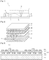
- FIG. 3 is a cross-section conceptual view illustrating the subject matter of a lighting device according to an exemplary embodiment of the present invention.
- FIG. 4 is an enlarged view of the subject matters for explaining the detailed configuration of the reflective unit in the structure of FIG. 3 .
- the lighting device may include: a plurality of LED light sources 130 formed on a printed circuit board 110; and a reflective unit 120 stacked on the printed circuit board 110 in a structure in which the LED light sources 130 penetrate, at an upper surface of the printed circuit board 110.
- a spaced area A1 is provided in an inner part of the reflective unit 120. The spaced area A1 may maximize luminance by improving the reflection efficiency of light emitted from the LED light sources 130.
- the reflective unit 120 may include: a first reflective film 121 and a second reflective film 122 which are disposed to oppose to each other; and a first adhesive pattern layer 123 which bonds the first and second reflective films, and in which a plurality of unit separation cells having a first spaced area formed in an inner part thereof are closely disposed to communicate with each other.
- the reflective unit may include the first reflective film 121 which is composed of a base substrate having a metal layer adhered to a surface of the printed circuit board 110 or white PET (polyethylen terephthalate); and the second reflective film 122 which is spaced apart from the first reflective film 121 to thereby form the first spaced area 123b and is formed of a transparent material.
- the first and second reflective films 121, 122 are stacked on the printed circuit board, and penetrate a hole formed on the reflective films so that the LED light source 130 is protruded to the outside.
- the first adhesive pattern layer 123 of a structure which is patterned on the first reflective film 121 is formed in a structure in which a plurality of unit separation cells C are disposed to adhere to each other.
- the unit air cell C forms an adhesive partition body 123a so that the first spaced area 123b is formed in the inner part of the unit air cell, and an upper surface thereof having the structure which forms the adhesive partition body 123a may be formed in an opened structure.
- each unit air cell C may be implemented in a structure in which at least one or more communication holes H are disposed to thereby communicate air between each unit air cell.
- the presence of the first adhesive pattern layer 123 which is formed in an adhered structure of the aforesaid unit separation cells C is resulted in maximizing reflectance during the process that light emitted from the light source is transmitted through the second reflective film formed of a transparent material, and is again reflected from the second reflective film.
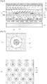
- the unit separation cells C may be implemented in a two-dimensional or three dimensional structure in which the plurality of the adhesive partition bodies 123a implementing a cavity in an inner part thereof are disposed, and the first spaced area 123b is implemented in a vacant structure in an inner side of the adhesive partition body 123a. That is, a cross-section of the adhesive partition body 123a may be implemented in various shapes such as a polygon, a circle, an ellipse and the like.
- each adhesive partition body 123a is disposed in a irregular structure so that the first spaced area 123b of an inner part of an unit separation member 123a and the second spaced area 123c of a vacant space between each unit separation member 123a may be implemented.
- reflection efficiency can be enhanced by a structure in which in the inner part of each unit air cell, the reflection light (arrow) of light is autonomously reflected within the first spaced area 123b, and (b) in particular, in a case where the communication hole H implemented in the present invention is implemented, the reflection efficiency of the reflection light (arrow) can be more improved through the communication hole.
- a structure of forming the communication hole of each unit air cell C may be implemented such that the communication hole is formed in one or more vertex parts, thereby achieving high efficiency. That is, it may be implemented so that three unit separation cells may communication with each other by one communication hole.
- the first reflective film 121 in which the adhesive pattern layer 123 is formed is a reflection construction which reflects light.
- the first reflective film may be modified in various structures.
- the second reflective film 122 formed of a transparent material is disposed on an upper part thereof.
- the second reflective film 122 may apply a film made of a transparent material such as PET and the like, and the spaced area may be formed by providing the first adhesive pattern layer 123 which separates the first and second reflective films 121, 122 from each other by patterning an adhesive material.
- the first reflective film 121 may have an optical film 126 which bonds a metal reflective layer 125 by the medium of an adhesive (i.e. a primer).
- the optical film 126 may be implemented in a structure which is stacked on a release film 128 by the medium of an adhesive material 127 (PSA).
- PSA adhesive material
- the metal reflective layer 125 may use Ag.
- the first reflective film 121 as the reflection construction which reflects light may use white PET (polyethylen terephthalate) in the present invention, particularly. That is, in the special reflective unit according to the present exemplary embodiment of the invention, the first reflective film may be implemented as general metal reflective material layers (Ag and the like). However, to achieve maximized effect of the improvement of luminance, white PET (polyethylen terephthalate) may be used (see FIG. 7 ).
- FIG. 7 is a result table for comparing a level in the improvement of luminance of the lighting device when the structure of the reflective unit according to the present exemplary embodiment of the invention is implemented.
- (A) is to measure luminance when only one reflective film implemented of Ag is formed on the surface of the printed circuit board, in the structure of FIG.
- (B) is to measure a result value of the improvement of luminance by comparing the conventional structure (A) with the structure of the reflective unit according to the present exemplary embodiment of the invention, namely, the structure in which an adhesive pattern material is formed of silicon to thereby form the pattern of FIG. 4 , and the first reflective film is an Ag film.
- (C) is to measure a result value of the improvement of luminance by comparing the conventional structure (A) with the structure in which the first reflective film is formed of white PET.
- luminance is 6605 and in standard of this, in the structure of (B), luminance is 7468, thereby showing the result of luminance improvement of about 13%.
- luminance is 8472, thereby showing a luminance increasing ratio of 28.6% compared to (A). That is, in the case of using the white PET while providing the structure (the first spaced area) in which the adhesive material layer is patterned, the maximized result of luminance improvement of luminance can be achieved.
- the second reflective film 122 may use a film made of a transparent material so that light emitted from the LED light source is transmitted onto the surface of the first reflective film 122 and is then reflected again.
- a reflective pattern 124 may be provided to a surface of the second reflective film 122 through white printing so that luminance can be improved by more promoting the dispersion of light.
- the reflective pattern may be provided so that the reflectance of light can be largely improved.
- the reflective pattern may be printed using a reflective ink including one of TiO 2 , CaCO 3 , BaSO 4 , Al 2 O 3 , Silicon, and PS.
- various kinds of light sources may be applied as light sources.
- an LED having a side-view light emitting type structure is used.
- the reflective pattern may be formed in a light emitting direction of the LED light source.
- the reflective pattern may be disposed such that as the reflective pattern gradually moves away from a light emitting direction of the LED light sources, a density of the reflective pattern becomes high.
- FIG. 8 illustrates the lighting device according another exemplary embodiment of the present invention.
- the second exemplary embodiment according to the present invention implements a structure in which a resin layer 140 is stacked on the printed circuit board.
- the configuration of the resin layer corresponds to the configuration which substitutes for a light guide plate of the lighting device, and functions to guide the light emitted from the light source forward.
- the lighting device may further include the plurality of LED light sources 130 formed on the printed circuit board 110, and the resin layer 140 for diffusing and guiding emitted light forward. That is, the resin layer 140 is stacked in a structure surrounding around the LED light sources and functions to disperse the light of the light sources emitted in a side direction. That is, the function of the conventional light guide plate may be performed by the resin layer 140.
- the resin layer may basically use any one if it is a resin made of a material which is able to diffuse light.
- a resin containing urethane arcrylrate oligomers as a main material may be used for a main material of the resin layer as one exemplary embodiment according to the present invention.
- a resin containing urethane arcrylrate oligomers as a main material may be used for a main material.
- a mixture of urethane arcrylrate oligomers which is a synthetic oligomer and a polymer type which is polyacryli may be used.
- a monomer mixing IBOA (isobornyl acrylate), HPA (Hydroxylpropyl acrylate), and 2-HEA (2-hydroxyethyl acrylate) which are low boiling point and diluted type reactive monomers may be further included.
- photoinitiators i.e. 1-hydroxycyclohexyl phenyl-ketone and the like
- the resin layer 140 may include a bead to improve the diffusion and reflection of light.
- the bead may range from 0.01 to 0.3 wt.% to a total weight of the resin layer. That is, the light emitted from the LED light source in the side direction is diffused and reflected through the resin layer 140 and the bead, thereby being capable of moving in an upper direction.
- a thickness occupied by the conventional light guide plate can be innovatively reduced, so a whole product can be thinner and can have a ductile material, thereby being capable of achieving generality that is applicable to a flexible display.
- the lighting device according to the present exemplary embodiment of the invention may be implemented in a structure in which an optical pattern layer 150 disposed on an upper part of the resin layer 140 and including an optical pattern 151 is provided.
- the optical pattern layer 150 may be include a second pattern layer 153 which forms a second spaced area 152 surrounding around the optical pattern. That is, the second adhesive pattern layer 153 forms a spaced space (i.e. the second spaced area) having a pattern in a fixed shape in the optical pattern 151 and is implemented by applying and bonding an adhesive material to remaining parts except for the space. That is, in a structure of the illustrated drawing, in a disposition relationship between the optical pattern layer 150 and the second adhesive pattern layer 153, the optical pattern layer 150 has a first substrate 150A and a second substrate 150B including the optical pattern in an inner part thereof. The first adhesive pattern layer 153 is applied to the remaining parts except for the second spaced area 152 surrounding around the light shielding pattern to thereby bond the first substrate 150A and the second substrate 150B.
- the second adhesive pattern layer 153 forms a spaced space (i.e. the second spaced area) having a pattern in a fixed shape in the optical pattern 151 and is implemented by applying and bonding an adhesive material to remaining parts except
- the optical pattern 151 may be formed as the light shielding pattern which is formed to prevent the concentration of light emitted from the LED light sources 130. For this, it is required to align between the optical pattern 151 and the LED light sources 130. After aligning is performed, it is bonded using an adhesive member for securing a fixing force.
- the first substrate 150A and the second substrate 150B may use a substrate made of a material having an excellent light transmission rate.
- PET may be used.
- the optical pattern 151 disposed between the first substrate 150A and the second substrate 150B may basically function not to concentrate the light emitted from the LED light sources, and may be implemented by performing light shielding printing on one of the first substrate 150A and the second substrate 150B. Aligning may be implemented by bonding two substrates using the adhesive layer coated with an adhesive material in the structure surrounding around the shielding pattern. That is, a bonded structure of the first substrate 150A and the second substrate 150B may also implement the function to fix the printed light shielding pattern 151.
- the adhesive layer may use a heat curing PSA, a heat curing adhesive, and an ultraviolet curing PSA type material.
- the adhesive material may prevent the occurrence of strong hot spots or dark spaces caused by overlapping the adhesive material on the light shielding pattern. Due to the presence of the spacing layer, the uniformity of light can be enhanced.
- the lighting device according to the present exemplary embodiment of the invention having the aforesaid structure may further include a diffusion plate 170 on an upper part of the resin layer, and a spacing module 160 having a third spaced area 161 between the diffusion plate 170 and the optical pattern layer 150.
- a prism sheet, a protective sheet and the like may be additionally provided to an upper part of the diffusion plate.
- FIG. 10 is to conceptually illustrate the configurations of the optical pattern 151 and the second adhesive pattern layer 153, and the second spaced area 152 formed by the same.
- the spaced space has a closed structure in which the spacing layer is formed. This is defined as "the second spaced area".
- a plane shape of the first spaced area 152 formed by the second adhesive pattern layer 153 may be implemented in various shapes such as a circle, an ellipse, a rectangle, a square, a polygon and the like.
- the adhesive pattern layer may be formed using a heat curing PSA, a heat curing adhesive, an ultraviolet curing PSA type material.
- the optical pattern 151 may be formed as the light shielding pattern so that light shielding effects can be implemented in a fixed part to prevent optical characteristics from being reduced due to the too strong strength of light or a phenomenon of the emission of yellowish light. That is, the light shielding pattern may be printed using a light shielding ink so that the concentration of light is not generated.
- the optical pattern may be implemented to adjust a light shielding level and a light diffusing level using only one optical pattern so that the optical pattern can perform the function to partially shield and diffuse light rather than the function to completely shield light.
- the optical pattern according to the present exemplary embodiment of the invention may be implemented in the overlapping printed structure of a complex pattern.
- the overlapping printed structure is called a structure which is implemented by forming one pattern and printing another pattern shape on an upper part thereof.
- the optical pattern may be implemented in the overlapping printed structure of: a diffusion pattern formed on a lower surface of a polymer film in a light emitting direction by using the light shielding ink including one or more materials selected from TiO 2 , CaCO 3 , BaSO 4 , Al 2 O 3 , and silicon; and a light shielding pattern using the light shielding ink including A1 or a mixture of A1 and TiO 2 . That is, the optical pattern may be configured such that after the diffusion pattern is formed by white-printing it on the surface of the polymer film, the light shielding pattern is formed thereon, or through an opposite order to this, the optical pattern may be formed in a double structure.
- the design for forming this pattern may be variously modified in consideration of the efficiency and strength of light and a light shielding ratio.
- the optical pattern may be formed in a triple structure in which the light shielding pattern that is a metal pattern is formed in a middle layer, and the diffusion pattern is implemented on its upper part and lower part, respectively.
- the optical pattern may be implemented by selecting the aforesaid materials.
- the optical pattern may secure the efficiency and uniformity of light through the triple structure in which one diffusion pattern is implemented using TiO 2 having an excellent refractive index, another diffusion pattern is implemented using CaCO 3 with TiO 2 having excellent light stability and color sensitivity, and the light shielding pattern is implemented using A1 having excellent obliterating power.
- CaCO 3 functions to finally implement white light through the function to reduce the exposure of yellowish light, so light having more stable efficiency can be implemented.
- inorganic materials having a large particle size and a similar structure such as BaSO 4 , Al 2 O 3 , Silicon beads and the like in addition to CaCO 3 may be utilized.
- the optical pattern may be formed by adjusting a density of the optical pattern so that as the LED light sources gradually get away from the light emitting direction, the density of the optical pattern is reduced.
- the lighting device according to the present exemplary embodiment of the invention may further include a spacing module disposed between the optical pattern layer 150 and the diffusion plate 170.
- FIG. 10 illustrates an implemented embodiment of the spacing module disposed between the optical pattern layer 150 and the diffusion plate 170 illustrated in FIG. 9 .
- a structure in which the spacing layer (the third spaced area 160) is provided between the optical pattern layer 150 and the diffusion plate 170 may be added. Thanks to the presence of the third spaced area 161, it may be achieved with the effects that the light emitted from the LED light sources can be diffused and uniformity of the light can be enhanced. Moreover, to minimize the deviation of light that penetrates the resin layer 140 and the optical pattern layer 150, a thickness of the third spaced area 160 may be formed in a range of 0.01 to 2mm.
- the third spaced area 160 may be formed by implementing a structure in which the spacing layer may be formed in a lower part of the diffusion plate.
- the third spaced area implemented by this structure is defined as "the spacing module”.
- the spacing module may include a method of implementing the spaced area (the spacing layer) by processing the diffusion plate itself or a configuration of forming the spaced area by forming a separate construction in the lower part of the diffusion plate. That is, as illustrated in FIG. 11-(a) , a spacer 171 is formed in the lower part of the diffusion plate 170 to thereby implement the third spaced area 160, or as illustrated in FIG. 11-(b) , the spacing module may be implemented in a structure of a bridge 172 in which the lower part of the diffusion plate is patterned to thereby adhere to a layer of the lower part, thereby forming the third spaced area 160.
- the integrated structure may be variously modified depending upon the patterned shape, namely, the shape of the pattern that forms the spaced area. According to this, it would be obvious that a shape of the bridge may be also variously modified. This is also included in the gist of the present invention.
- the spacing module may be also implemented in a structure that forms the spaced area 160 using a separate construction.
- the illustrated construction is a spacer member and shows an example of the structure that forms the bridge 174.
- the gist of the present invention includes this method, and various modified embodiments which may implement the spacing layer in the lower part of the diffusion plate fall also into the gist of the present invention.
- the spaced areas 160, 161 may be formed as a plurality of layers by employing structures 175, 176 which may implement an independent spacing layer.
- the lighting device may implement a disposition structure of the LED light sources 130 emitting light as illustrated in FIG. 5 . That is, to reduce the number of light sources, the LED light sources 130 may be disposed by applying a side-view light emitting type LED.
- the aforesaid lighting device may be applied to an LCD through the following configurations and functions.
- light is emitted from the side-view light emitting type LED light source 130 in a side direction, the emitted light is reflected and diffused on the resin layer 140 formed instead of the conventional light guide plate. Concentration of the light can be prevented by the optical pattern layer 150, and deviation of the light can be minimized by the third spaced area formed in the lower part of the diffusion plate.
- the control of reflectance may be implemented by varying a design which implements the spaced area by patterning the adhesive material layer.
- the implementation of different reflectance and colors can be adjusted depending upon a raw material and kind of the patterned adhesive material.
- reflectance may be adjusted depending upon optical characteristics and a thickness of the second reflective film 122.
- the light can be induced forward.
- the light passing through the resin layer 140 is diffused or shielded through the optical pattern 151 formed on the optical pattern layer 150.
- optical characteristics of the refined light is refined once again through the spacing module formed in the lower part of the diffusion plate, thereby increasing uniformity.
- the light is incident to an LCD panel as white light through an optical sheet such as a prism sheet 180 and a DBEF 190 which are added later.
- the lighting device thanks to the structure of the reflective unit having the spaced area, reflection efficiency can be maximized. Furthermore, when implementing the lighting device, the light guide plate is removed, the side-view light emitting type LED is applied as the supply source of light, by diffusing and reflecting light through the resin layer, the light is guided, thereby making a product thin and reducing the number of light sources. Meanwhile, due to the deterioration of luminance and the problem of uniformity caused by the reduction of the light sources may be adjusted by providing the reflective pattern, the shielding pattern and the spaced area of the spacing module, so optical characteristics can be improved.
Landscapes
- Physics & Mathematics (AREA)
- Nonlinear Science (AREA)
- General Physics & Mathematics (AREA)
- Optics & Photonics (AREA)
- Mathematical Physics (AREA)
- Chemical & Material Sciences (AREA)
- Crystallography & Structural Chemistry (AREA)
- Planar Illumination Modules (AREA)
- Liquid Crystal (AREA)
- Led Device Packages (AREA)
- Fastening Of Light Sources Or Lamp Holders (AREA)
- Non-Portable Lighting Devices Or Systems Thereof (AREA)
Applications Claiming Priority (3)
| Application Number | Priority Date | Filing Date | Title |
|---|---|---|---|
| KR20110076259 | 2011-07-29 | ||
| KR1020120017285A KR101357583B1 (ko) | 2011-07-29 | 2012-02-21 | 조명장치 및 이를 이용한 액정표시장치 |
| PCT/KR2012/005980 WO2013019025A2 (en) | 2011-07-29 | 2012-07-26 | Lighting device and liquid crystal display using the same |
Publications (3)
| Publication Number | Publication Date |
|---|---|
| EP2737244A2 EP2737244A2 (en) | 2014-06-04 |
| EP2737244A4 EP2737244A4 (en) | 2015-04-22 |
| EP2737244B1 true EP2737244B1 (en) | 2017-09-06 |
Family
ID=47894594
Family Applications (1)
| Application Number | Title | Priority Date | Filing Date |
|---|---|---|---|
| EP12820135.7A Active EP2737244B1 (en) | 2011-07-29 | 2012-07-26 | Lighting device and liquid crystal display using the same |
Country Status (7)
| Country | Link |
|---|---|
| US (1) | US9757924B2 (ko) |
| EP (1) | EP2737244B1 (ko) |
| JP (2) | JP5947892B2 (ko) |
| KR (1) | KR101357583B1 (ko) |
| CN (2) | CN106249477B (ko) |
| TW (1) | TWI493257B (ko) |
| WO (1) | WO2013019025A2 (ko) |
Families Citing this family (20)
| Publication number | Priority date | Publication date | Assignee | Title |
|---|---|---|---|---|
| US8562770B2 (en) | 2008-05-21 | 2013-10-22 | Manufacturing Resources International, Inc. | Frame seal methods for LCD |
| US9573346B2 (en) | 2008-05-21 | 2017-02-21 | Manufacturing Resources International, Inc. | Photoinitiated optical adhesive and method for using same |
| JP2012529081A (ja) | 2009-06-03 | 2012-11-15 | マニュファクチャリング・リソーシズ・インターナショナル・インコーポレーテッド | Ledバックライトの動的減光 |
| CN103133918B (zh) * | 2011-11-23 | 2015-11-11 | 财团法人工业技术研究院 | 面光源以及可挠性面光源 |
| CN103032766A (zh) * | 2012-12-12 | 2013-04-10 | 京东方科技集团股份有限公司 | 一种背光模组以及显示装置 |
| US9348174B2 (en) | 2013-03-14 | 2016-05-24 | Manufacturing Resources International, Inc. | Rigid LCD assembly |
| FR3005340B1 (fr) * | 2013-05-03 | 2017-09-22 | Appareillage & Bobinage Electrique Du Limousin | Luminaire a del et candelabre equipe d'un tel luminaire |
| US9690137B2 (en) | 2013-07-03 | 2017-06-27 | Manufacturing Resources International, Inc. | Airguide backlight assembly |
| KR102091621B1 (ko) * | 2013-07-12 | 2020-04-14 | 엘지이노텍 주식회사 | 조명장치 |
| US10191212B2 (en) | 2013-12-02 | 2019-01-29 | Manufacturing Resources International, Inc. | Expandable light guide for backlight |
| US10527276B2 (en) | 2014-04-17 | 2020-01-07 | Manufacturing Resources International, Inc. | Rod as a lens element for light emitting diodes |
| US10649273B2 (en) | 2014-10-08 | 2020-05-12 | Manufacturing Resources International, Inc. | LED assembly for transparent liquid crystal display and static graphic |
| US20160202395A1 (en) * | 2015-01-14 | 2016-07-14 | Samsung Display Co., Ltd. | Display apparatus with improved viewing angle |
| US10261362B2 (en) | 2015-09-01 | 2019-04-16 | Manufacturing Resources International, Inc. | Optical sheet tensioner |
| JP6741437B2 (ja) * | 2016-02-16 | 2020-08-19 | 株式会社デンソーテン | スイッチ装置 |
| KR102594498B1 (ko) * | 2016-09-30 | 2023-10-25 | 엘지디스플레이 주식회사 | 액정표시장치 |
| CN108008558B (zh) * | 2017-11-28 | 2019-12-10 | 信利光电股份有限公司 | 一种触摸屏及其制作方法 |
| KR102342626B1 (ko) | 2018-03-13 | 2021-12-23 | 애플 인크. | 직하형 백라이트 유닛들을 갖는 디스플레이들 |
| US10816850B2 (en) * | 2018-04-20 | 2020-10-27 | Wuhan China Star Optoelectronics Technology Co., Ltd. | Direct-lit backlight module and manufacturing method thereof |
| US11175016B2 (en) * | 2018-09-13 | 2021-11-16 | Minebea Mitsumi Inc. | Planar illumination device with spacer between lens and diffuser |
Family Cites Families (52)
| Publication number | Priority date | Publication date | Assignee | Title |
|---|---|---|---|---|
| US3861135A (en) * | 1973-02-08 | 1975-01-21 | Chomerics Inc | Electrical interconnector and method of making |
| JP2930820B2 (ja) * | 1992-10-20 | 1999-08-09 | 富士通株式会社 | 携帯端末装置用液晶ディスプレイモジュール |
| DE4417990B4 (de) * | 1994-05-21 | 2004-11-11 | Siemens Ag | Flüssigkristallanzeige |
| JPH09202871A (ja) * | 1996-01-25 | 1997-08-05 | Lintec Corp | 面光源体用粘着剤及びそれを用いた面光源体 |
| JPH10160938A (ja) | 1996-11-29 | 1998-06-19 | Toshiba Lighting & Technol Corp | 導光ユニット、バックライト及びこれを用いた照明装置 |
| JP4101339B2 (ja) * | 1997-09-25 | 2008-06-18 | 大日本印刷株式会社 | 光拡散フィルム、その製造方法、拡散層付偏光板及び液晶表示装置 |
| JP2000180633A (ja) * | 1998-12-16 | 2000-06-30 | Shiseido Co Ltd | 導光板、照明装置および液晶表示装置 |
| WO2001061383A1 (fr) * | 2000-02-16 | 2001-08-23 | Matsushita Electric Industrial Co., Ltd. | Corps a forme irreguliere, feuille reflechissante et element d'affichage a cristaux liquides de type reflechissant, et dispositif et procede de production correspondants |
| JP4271928B2 (ja) * | 2001-11-16 | 2009-06-03 | 株式会社きもと | 光反射材料及びそれを用いた光源装置 |
| US7009771B2 (en) * | 2002-05-16 | 2006-03-07 | Eastman Kodak Company | Optical element containing an optical spacer |
| JP2004095422A (ja) * | 2002-09-02 | 2004-03-25 | Sharp Corp | 照明装置 |
| JP2004179116A (ja) * | 2002-11-29 | 2004-06-24 | Alps Electric Co Ltd | 背面照明装置及び液晶表示装置 |
| US6871982B2 (en) | 2003-01-24 | 2005-03-29 | Digital Optics International Corporation | High-density illumination system |
| KR100541533B1 (ko) * | 2003-06-25 | 2006-01-11 | 엘지.필립스 엘시디 주식회사 | 액정표시장치용 백라이트 |
| US20050116235A1 (en) * | 2003-12-02 | 2005-06-02 | Schultz John C. | Illumination assembly |
| US7967492B2 (en) * | 2005-02-28 | 2011-06-28 | Kuraray Co., Ltd. | Light diffusion film and planar light source element and liquid crystal display device utilizing the same |
| KR101203519B1 (ko) * | 2005-06-28 | 2012-11-22 | 엘지디스플레이 주식회사 | 백라이트 및 이를 구비한 액정표시장치 |
| KR20070010478A (ko) * | 2005-07-19 | 2007-01-24 | 삼성전자주식회사 | 광학시트, 이를 갖는 백라이트 어셈블리 및 이를 갖는표시장치 |
| JP4467493B2 (ja) * | 2005-09-16 | 2010-05-26 | シャープ株式会社 | バックライト装置及びこれを備える表示装置 |
| WO2007055059A1 (ja) * | 2005-11-08 | 2007-05-18 | Sharp Kabushiki Kaisha | ランプホルダ並びにこれを用いたバックライト装置及び液晶表示装置 |
| EP1957858A4 (en) | 2005-11-29 | 2010-11-24 | Showa Denko Kk | REFLECTOR FRAME, FLAT LIGHT SOURCE EQUIPMENT PROVIDED WITH THE REFLECTOR FRAME, AND LIGHT DISPLAY EQUIPMENT USING THE FLAT LIGHT SOURCE SOURCE |
| KR100761055B1 (ko) * | 2005-12-09 | 2007-09-21 | 주식회사 우영 | 직하형 led 백라이트 유닛 |
| KR101220204B1 (ko) * | 2005-12-28 | 2013-01-09 | 엘지디스플레이 주식회사 | 엘이디 백라이트어셈블리 및 이를 이용한 액정표시장치모듈 |
| KR100821042B1 (ko) * | 2006-09-22 | 2008-04-08 | 삼성에스디아이 주식회사 | 액정표시장치 및 이를 이용한 휴대용 표시기기 |
| KR20080032506A (ko) * | 2006-10-10 | 2008-04-15 | 삼성전자주식회사 | 백라이트 유닛 및 이를 이용한 액정 표시 장치 |
| WO2008044170A2 (en) * | 2006-10-10 | 2008-04-17 | Koninklijke Philips Electronics N.V. | Thin illumination device, display device and luminary device |
| TWI360695B (en) * | 2006-10-20 | 2012-03-21 | Chimei Innolux Corp | Direct type backlight unit and liquid crystal disp |
| KR20080043905A (ko) * | 2006-11-15 | 2008-05-20 | 엘지전자 주식회사 | 디스플레이 패널용 백라이트 유닛 |
| JP4228026B2 (ja) | 2007-02-28 | 2009-02-25 | 日東電工株式会社 | バックライトシステムおよび粘着剤付光学シート |
| CN101276871B (zh) * | 2007-03-29 | 2012-08-29 | 晶元光电股份有限公司 | 光电元件、背光模块装置和照明装置 |
| JP2008304831A (ja) * | 2007-06-11 | 2008-12-18 | Toppan Printing Co Ltd | 光学部材およびその製造方法 |
| JP2009169400A (ja) * | 2007-12-18 | 2009-07-30 | Sony Corp | 表示装置および電子機器 |
| JP2009150940A (ja) * | 2007-12-18 | 2009-07-09 | Toppan Printing Co Ltd | 光学シート、バックライトユニット、バックライト装置及びディスプレイ装置 |
| US7845826B2 (en) | 2008-01-15 | 2010-12-07 | Skc Haas Display Films Co., Ltd. | Multilayered integrated backlight illumination assembly |
| CN201170472Y (zh) | 2008-03-14 | 2008-12-24 | 上海广电光电子有限公司 | 直下式背光模组 |
| TWI364557B (en) * | 2008-05-02 | 2012-05-21 | Chimei Innolux Corp | Light source and backlight module and liquid crystal display device using same |
| KR20100035783A (ko) * | 2008-09-29 | 2010-04-07 | 삼성전자주식회사 | 편광기, 이의 제조 방법, 이 편광기를 갖는 표시기판 및 백라이트 어셈블리 |
| KR101579815B1 (ko) * | 2008-11-27 | 2015-12-28 | 삼성디스플레이 주식회사 | 액정 표시 장치 |
| JP2010135204A (ja) * | 2008-12-05 | 2010-06-17 | Citizen Electronics Co Ltd | 面状光源及び液晶表示装置 |
| EP2422237A4 (en) | 2009-04-21 | 2012-10-17 | Lg Electronics Inc | LIGHT EMITTING DEVICE |
| KR20100011137U (ko) * | 2009-05-06 | 2010-11-16 | 주식회사 삼진엘앤디 | 공기층을 가지는 도광판 |
| CN101586749A (zh) * | 2009-06-11 | 2009-11-25 | 浙江西子光电科技有限公司 | Led照明装置及其散热结构 |
| EP2470951B1 (en) * | 2009-08-27 | 2016-07-27 | LG Electronics Inc. | Backlight unit and display device |
| KR100964467B1 (ko) | 2009-11-24 | 2010-06-16 | 엘지전자 주식회사 | 디스플레이 장치 |
| JP5540610B2 (ja) * | 2009-09-03 | 2014-07-02 | 株式会社Jvcケンウッド | 光量制御部材、面光源装置及び表示装置 |
| JP5402428B2 (ja) * | 2009-09-09 | 2014-01-29 | オムロン株式会社 | 面光源装置及び液晶表示装置 |
| KR20110038191A (ko) * | 2009-10-07 | 2011-04-14 | 엘지디스플레이 주식회사 | 엘이디 백라이트 유닛 및 이를 이용한 액정표시장치 |
| TWI392931B (zh) | 2009-11-09 | 2013-04-11 | Au Optronics Corp | 發光裝置 |
| CN201661930U (zh) * | 2009-11-12 | 2010-12-01 | 金芃 | 一种led侧光式背光源的发光元件 |
| EP2354836B1 (en) * | 2009-12-14 | 2018-08-08 | Harman Becker Automotive Systems GmbH | Display unit with an integrated backlight |
| KR20110085722A (ko) * | 2010-01-21 | 2011-07-27 | 삼성엘이디 주식회사 | 백라이트 유닛 및 이를 구비한 액정 표시 장치 |
| WO2012138123A2 (ko) * | 2011-04-04 | 2012-10-11 | 엘지이노텍 주식회사 | 조명장치 |
-
2012
- 2012-02-21 KR KR1020120017285A patent/KR101357583B1/ko active IP Right Grant
- 2012-07-26 EP EP12820135.7A patent/EP2737244B1/en active Active
- 2012-07-26 CN CN201610573115.9A patent/CN106249477B/zh active Active
- 2012-07-26 US US13/558,949 patent/US9757924B2/en active Active
- 2012-07-26 CN CN201280037976.5A patent/CN103732975B/zh active Active
- 2012-07-26 WO PCT/KR2012/005980 patent/WO2013019025A2/en active Application Filing
- 2012-07-26 JP JP2014522754A patent/JP5947892B2/ja active Active
- 2012-07-27 TW TW101127159A patent/TWI493257B/zh active
-
2016
- 2016-06-09 JP JP2016115208A patent/JP6246860B2/ja active Active
Non-Patent Citations (1)
| Title |
|---|
| None * |
Also Published As
| Publication number | Publication date |
|---|---|
| US9757924B2 (en) | 2017-09-12 |
| WO2013019025A2 (en) | 2013-02-07 |
| US20130027633A1 (en) | 2013-01-31 |
| JP6246860B2 (ja) | 2017-12-13 |
| CN103732975B (zh) | 2016-08-17 |
| JP2016213195A (ja) | 2016-12-15 |
| JP5947892B2 (ja) | 2016-07-06 |
| WO2013019025A3 (en) | 2013-04-04 |
| TW201314317A (zh) | 2013-04-01 |
| CN106249477A (zh) | 2016-12-21 |
| EP2737244A4 (en) | 2015-04-22 |
| CN103732975A (zh) | 2014-04-16 |
| EP2737244A2 (en) | 2014-06-04 |
| TWI493257B (zh) | 2015-07-21 |
| KR20130014326A (ko) | 2013-02-07 |
| CN106249477B (zh) | 2019-11-29 |
| KR101357583B1 (ko) | 2014-02-05 |
| JP2014522082A (ja) | 2014-08-28 |
Similar Documents
| Publication | Publication Date | Title |
|---|---|---|
| EP2737244B1 (en) | Lighting device and liquid crystal display using the same | |
| JP7383780B2 (ja) | 照明装置 | |
| US9778506B2 (en) | Lighting device with enhanced optical properties and liquid crystal display device having the lighting device | |
| KR102215971B1 (ko) | 조명장치 | |
| KR101829306B1 (ko) | 조명장치 | |
| KR101829305B1 (ko) | 조명장치 | |
| KR20180134825A (ko) | 조명장치 | |
| KR101399039B1 (ko) | 조명장치 및 이를 포함하는 액정표시장치 | |
| KR102601097B1 (ko) | 조명장치 | |
| KR101930852B1 (ko) | 조명장치 | |
| US11994768B2 (en) | Lighting apparatus | |
| KR101947532B1 (ko) | 조명장치 | |
| KR20210019042A (ko) | 조명장치 | |
| KR101399048B1 (ko) | 조명장치 및 이를 이용한 액정표시장치 | |
| KR20190016050A (ko) | 조명장치 |
Legal Events
| Date | Code | Title | Description |
|---|---|---|---|
| PUAI | Public reference made under article 153(3) epc to a published international application that has entered the european phase |
Free format text: ORIGINAL CODE: 0009012 |
|
| 17P | Request for examination filed |
Effective date: 20140122 |
|
| AK | Designated contracting states |
Kind code of ref document: A2 Designated state(s): AL AT BE BG CH CY CZ DE DK EE ES FI FR GB GR HR HU IE IS IT LI LT LU LV MC MK MT NL NO PL PT RO RS SE SI SK SM TR |
|
| DAX | Request for extension of the european patent (deleted) | ||
| A4 | Supplementary search report drawn up and despatched |
Effective date: 20150320 |
|
| RIC1 | Information provided on ipc code assigned before grant |
Ipc: G02F 1/13357 20060101ALI20150316BHEP Ipc: F21V 5/00 20150101ALI20150316BHEP Ipc: F21Y 101/02 20060101ALI20150316BHEP Ipc: F21S 2/00 20060101AFI20150316BHEP |
|
| GRAP | Despatch of communication of intention to grant a patent |
Free format text: ORIGINAL CODE: EPIDOSNIGR1 |
|
| RIC1 | Information provided on ipc code assigned before grant |
Ipc: G02F 1/13357 20060101ALI20170307BHEP Ipc: F21S 2/00 20160101AFI20170307BHEP Ipc: F21V 5/00 20150101ALI20170307BHEP |
|
| INTG | Intention to grant announced |
Effective date: 20170331 |
|
| RAP1 | Party data changed (applicant data changed or rights of an application transferred) |
Owner name: LG INNOTEK CO., LTD. |
|
| GRAS | Grant fee paid |
Free format text: ORIGINAL CODE: EPIDOSNIGR3 |
|
| GRAA | (expected) grant |
Free format text: ORIGINAL CODE: 0009210 |
|
| AK | Designated contracting states |
Kind code of ref document: B1 Designated state(s): AL AT BE BG CH CY CZ DE DK EE ES FI FR GB GR HR HU IE IS IT LI LT LU LV MC MK MT NL NO PL PT RO RS SE SI SK SM TR |
|
| REG | Reference to a national code |
Ref country code: GB Ref legal event code: FG4D |
|
| REG | Reference to a national code |
Ref country code: CH Ref legal event code: EP Ref country code: AT Ref legal event code: REF Ref document number: 926281 Country of ref document: AT Kind code of ref document: T Effective date: 20170915 |
|
| REG | Reference to a national code |
Ref country code: IE Ref legal event code: FG4D |
|
| REG | Reference to a national code |
Ref country code: DE Ref legal event code: R096 Ref document number: 602012037088 Country of ref document: DE |
|
| REG | Reference to a national code |
Ref country code: NL Ref legal event code: FP |
|
| REG | Reference to a national code |
Ref country code: LT Ref legal event code: MG4D |
|
| PG25 | Lapsed in a contracting state [announced via postgrant information from national office to epo] |
Ref country code: SE Free format text: LAPSE BECAUSE OF FAILURE TO SUBMIT A TRANSLATION OF THE DESCRIPTION OR TO PAY THE FEE WITHIN THE PRESCRIBED TIME-LIMIT Effective date: 20170906 Ref country code: NO Free format text: LAPSE BECAUSE OF FAILURE TO SUBMIT A TRANSLATION OF THE DESCRIPTION OR TO PAY THE FEE WITHIN THE PRESCRIBED TIME-LIMIT Effective date: 20171206 Ref country code: HR Free format text: LAPSE BECAUSE OF FAILURE TO SUBMIT A TRANSLATION OF THE DESCRIPTION OR TO PAY THE FEE WITHIN THE PRESCRIBED TIME-LIMIT Effective date: 20170906 Ref country code: LT Free format text: LAPSE BECAUSE OF FAILURE TO SUBMIT A TRANSLATION OF THE DESCRIPTION OR TO PAY THE FEE WITHIN THE PRESCRIBED TIME-LIMIT Effective date: 20170906 Ref country code: FI Free format text: LAPSE BECAUSE OF FAILURE TO SUBMIT A TRANSLATION OF THE DESCRIPTION OR TO PAY THE FEE WITHIN THE PRESCRIBED TIME-LIMIT Effective date: 20170906 |
|
| REG | Reference to a national code |
Ref country code: AT Ref legal event code: MK05 Ref document number: 926281 Country of ref document: AT Kind code of ref document: T Effective date: 20170906 |
|
| PG25 | Lapsed in a contracting state [announced via postgrant information from national office to epo] |
Ref country code: GR Free format text: LAPSE BECAUSE OF FAILURE TO SUBMIT A TRANSLATION OF THE DESCRIPTION OR TO PAY THE FEE WITHIN THE PRESCRIBED TIME-LIMIT Effective date: 20171207 Ref country code: RS Free format text: LAPSE BECAUSE OF FAILURE TO SUBMIT A TRANSLATION OF THE DESCRIPTION OR TO PAY THE FEE WITHIN THE PRESCRIBED TIME-LIMIT Effective date: 20170906 Ref country code: LV Free format text: LAPSE BECAUSE OF FAILURE TO SUBMIT A TRANSLATION OF THE DESCRIPTION OR TO PAY THE FEE WITHIN THE PRESCRIBED TIME-LIMIT Effective date: 20170906 Ref country code: BG Free format text: LAPSE BECAUSE OF FAILURE TO SUBMIT A TRANSLATION OF THE DESCRIPTION OR TO PAY THE FEE WITHIN THE PRESCRIBED TIME-LIMIT Effective date: 20171206 Ref country code: ES Free format text: LAPSE BECAUSE OF FAILURE TO SUBMIT A TRANSLATION OF THE DESCRIPTION OR TO PAY THE FEE WITHIN THE PRESCRIBED TIME-LIMIT Effective date: 20170906 |
|
| PG25 | Lapsed in a contracting state [announced via postgrant information from national office to epo] |
Ref country code: CZ Free format text: LAPSE BECAUSE OF FAILURE TO SUBMIT A TRANSLATION OF THE DESCRIPTION OR TO PAY THE FEE WITHIN THE PRESCRIBED TIME-LIMIT Effective date: 20170906 Ref country code: PL Free format text: LAPSE BECAUSE OF FAILURE TO SUBMIT A TRANSLATION OF THE DESCRIPTION OR TO PAY THE FEE WITHIN THE PRESCRIBED TIME-LIMIT Effective date: 20170906 Ref country code: RO Free format text: LAPSE BECAUSE OF FAILURE TO SUBMIT A TRANSLATION OF THE DESCRIPTION OR TO PAY THE FEE WITHIN THE PRESCRIBED TIME-LIMIT Effective date: 20170906 |
|
| PG25 | Lapsed in a contracting state [announced via postgrant information from national office to epo] |
Ref country code: SK Free format text: LAPSE BECAUSE OF FAILURE TO SUBMIT A TRANSLATION OF THE DESCRIPTION OR TO PAY THE FEE WITHIN THE PRESCRIBED TIME-LIMIT Effective date: 20170906 Ref country code: IS Free format text: LAPSE BECAUSE OF FAILURE TO SUBMIT A TRANSLATION OF THE DESCRIPTION OR TO PAY THE FEE WITHIN THE PRESCRIBED TIME-LIMIT Effective date: 20180106 Ref country code: IT Free format text: LAPSE BECAUSE OF FAILURE TO SUBMIT A TRANSLATION OF THE DESCRIPTION OR TO PAY THE FEE WITHIN THE PRESCRIBED TIME-LIMIT Effective date: 20170906 Ref country code: EE Free format text: LAPSE BECAUSE OF FAILURE TO SUBMIT A TRANSLATION OF THE DESCRIPTION OR TO PAY THE FEE WITHIN THE PRESCRIBED TIME-LIMIT Effective date: 20170906 Ref country code: AT Free format text: LAPSE BECAUSE OF FAILURE TO SUBMIT A TRANSLATION OF THE DESCRIPTION OR TO PAY THE FEE WITHIN THE PRESCRIBED TIME-LIMIT Effective date: 20170906 Ref country code: SM Free format text: LAPSE BECAUSE OF FAILURE TO SUBMIT A TRANSLATION OF THE DESCRIPTION OR TO PAY THE FEE WITHIN THE PRESCRIBED TIME-LIMIT Effective date: 20170906 |
|
| REG | Reference to a national code |
Ref country code: DE Ref legal event code: R097 Ref document number: 602012037088 Country of ref document: DE |
|
| REG | Reference to a national code |
Ref country code: FR Ref legal event code: PLFP Year of fee payment: 7 |
|
| PLBE | No opposition filed within time limit |
Free format text: ORIGINAL CODE: 0009261 |
|
| STAA | Information on the status of an ep patent application or granted ep patent |
Free format text: STATUS: NO OPPOSITION FILED WITHIN TIME LIMIT |
|
| PG25 | Lapsed in a contracting state [announced via postgrant information from national office to epo] |
Ref country code: DK Free format text: LAPSE BECAUSE OF FAILURE TO SUBMIT A TRANSLATION OF THE DESCRIPTION OR TO PAY THE FEE WITHIN THE PRESCRIBED TIME-LIMIT Effective date: 20170906 |
|
| 26N | No opposition filed |
Effective date: 20180607 |
|
| PG25 | Lapsed in a contracting state [announced via postgrant information from national office to epo] |
Ref country code: SI Free format text: LAPSE BECAUSE OF FAILURE TO SUBMIT A TRANSLATION OF THE DESCRIPTION OR TO PAY THE FEE WITHIN THE PRESCRIBED TIME-LIMIT Effective date: 20170906 |
|
| REG | Reference to a national code |
Ref country code: CH Ref legal event code: PL |
|
| PG25 | Lapsed in a contracting state [announced via postgrant information from national office to epo] |
Ref country code: MC Free format text: LAPSE BECAUSE OF FAILURE TO SUBMIT A TRANSLATION OF THE DESCRIPTION OR TO PAY THE FEE WITHIN THE PRESCRIBED TIME-LIMIT Effective date: 20170906 Ref country code: LU Free format text: LAPSE BECAUSE OF NON-PAYMENT OF DUE FEES Effective date: 20180726 |
|
| REG | Reference to a national code |
Ref country code: BE Ref legal event code: MM Effective date: 20180731 |
|
| REG | Reference to a national code |
Ref country code: IE Ref legal event code: MM4A |
|
| PG25 | Lapsed in a contracting state [announced via postgrant information from national office to epo] |
Ref country code: IE Free format text: LAPSE BECAUSE OF NON-PAYMENT OF DUE FEES Effective date: 20180726 Ref country code: LI Free format text: LAPSE BECAUSE OF NON-PAYMENT OF DUE FEES Effective date: 20180731 Ref country code: CH Free format text: LAPSE BECAUSE OF NON-PAYMENT OF DUE FEES Effective date: 20180731 |
|
| PG25 | Lapsed in a contracting state [announced via postgrant information from national office to epo] |
Ref country code: BE Free format text: LAPSE BECAUSE OF NON-PAYMENT OF DUE FEES Effective date: 20180731 |
|
| PG25 | Lapsed in a contracting state [announced via postgrant information from national office to epo] |
Ref country code: MT Free format text: LAPSE BECAUSE OF NON-PAYMENT OF DUE FEES Effective date: 20180726 |
|
| PG25 | Lapsed in a contracting state [announced via postgrant information from national office to epo] |
Ref country code: TR Free format text: LAPSE BECAUSE OF FAILURE TO SUBMIT A TRANSLATION OF THE DESCRIPTION OR TO PAY THE FEE WITHIN THE PRESCRIBED TIME-LIMIT Effective date: 20170906 |
|
| PG25 | Lapsed in a contracting state [announced via postgrant information from national office to epo] |
Ref country code: HU Free format text: LAPSE BECAUSE OF FAILURE TO SUBMIT A TRANSLATION OF THE DESCRIPTION OR TO PAY THE FEE WITHIN THE PRESCRIBED TIME-LIMIT; INVALID AB INITIO Effective date: 20120726 Ref country code: PT Free format text: LAPSE BECAUSE OF FAILURE TO SUBMIT A TRANSLATION OF THE DESCRIPTION OR TO PAY THE FEE WITHIN THE PRESCRIBED TIME-LIMIT Effective date: 20170906 |
|
| PG25 | Lapsed in a contracting state [announced via postgrant information from national office to epo] |
Ref country code: MK Free format text: LAPSE BECAUSE OF NON-PAYMENT OF DUE FEES Effective date: 20170906 Ref country code: CY Free format text: LAPSE BECAUSE OF FAILURE TO SUBMIT A TRANSLATION OF THE DESCRIPTION OR TO PAY THE FEE WITHIN THE PRESCRIBED TIME-LIMIT Effective date: 20170906 |
|
| PG25 | Lapsed in a contracting state [announced via postgrant information from national office to epo] |
Ref country code: AL Free format text: LAPSE BECAUSE OF FAILURE TO SUBMIT A TRANSLATION OF THE DESCRIPTION OR TO PAY THE FEE WITHIN THE PRESCRIBED TIME-LIMIT Effective date: 20170906 |
|
| PGFP | Annual fee paid to national office [announced via postgrant information from national office to epo] |
Ref country code: NL Payment date: 20230621 Year of fee payment: 12 Ref country code: FR Payment date: 20230621 Year of fee payment: 12 |
|
| PGFP | Annual fee paid to national office [announced via postgrant information from national office to epo] |
Ref country code: GB Payment date: 20230620 Year of fee payment: 12 |
|
| PGFP | Annual fee paid to national office [announced via postgrant information from national office to epo] |
Ref country code: DE Payment date: 20230620 Year of fee payment: 12 |