EP2728512A2 - Kapazitative Bilderfassungsvorrichtung mit aktiven Pixelnzum Erfassen - Google Patents
Kapazitative Bilderfassungsvorrichtung mit aktiven Pixelnzum Erfassen Download PDFInfo
- Publication number
- EP2728512A2 EP2728512A2 EP13191016.8A EP13191016A EP2728512A2 EP 2728512 A2 EP2728512 A2 EP 2728512A2 EP 13191016 A EP13191016 A EP 13191016A EP 2728512 A2 EP2728512 A2 EP 2728512A2
- Authority
- EP
- European Patent Office
- Prior art keywords
- sensor
- data line
- insulator layer
- transistor
- source follower
- Prior art date
- Legal status (The legal status is an assumption and is not a legal conclusion. Google has not performed a legal analysis and makes no representation as to the accuracy of the status listed.)
- Granted
Links
Images



Classifications
-
- G—PHYSICS
- G06—COMPUTING OR CALCULATING; COUNTING
- G06F—ELECTRIC DIGITAL DATA PROCESSING
- G06F3/00—Input arrangements for transferring data to be processed into a form capable of being handled by the computer; Output arrangements for transferring data from processing unit to output unit, e.g. interface arrangements
- G06F3/01—Input arrangements or combined input and output arrangements for interaction between user and computer
- G06F3/03—Arrangements for converting the position or the displacement of a member into a coded form
- G06F3/041—Digitisers, e.g. for touch screens or touch pads, characterised by the transducing means
- G06F3/044—Digitisers, e.g. for touch screens or touch pads, characterised by the transducing means by capacitive means
- G06F3/0443—Digitisers, e.g. for touch screens or touch pads, characterised by the transducing means by capacitive means using a single layer of sensing electrodes
-
- G—PHYSICS
- G01—MEASURING; TESTING
- G01R—MEASURING ELECTRIC VARIABLES; MEASURING MAGNETIC VARIABLES
- G01R27/00—Arrangements for measuring resistance, reactance, impedance, or electric characteristics derived therefrom
- G01R27/02—Measuring real or complex resistance, reactance, impedance, or other two-pole characteristics derived therefrom, e.g. time constant
- G01R27/26—Measuring inductance or capacitance; Measuring quality factor, e.g. by using the resonance method; Measuring loss factor; Measuring dielectric constants ; Measuring impedance or related variables
- G01R27/2605—Measuring capacitance
-
- G—PHYSICS
- G06—COMPUTING OR CALCULATING; COUNTING
- G06F—ELECTRIC DIGITAL DATA PROCESSING
- G06F3/00—Input arrangements for transferring data to be processed into a form capable of being handled by the computer; Output arrangements for transferring data from processing unit to output unit, e.g. interface arrangements
- G06F3/01—Input arrangements or combined input and output arrangements for interaction between user and computer
- G06F3/03—Arrangements for converting the position or the displacement of a member into a coded form
- G06F3/041—Digitisers, e.g. for touch screens or touch pads, characterised by the transducing means
- G06F3/044—Digitisers, e.g. for touch screens or touch pads, characterised by the transducing means by capacitive means
- G06F3/0446—Digitisers, e.g. for touch screens or touch pads, characterised by the transducing means by capacitive means using a grid-like structure of electrodes in at least two directions, e.g. using row and column electrodes
-
- G—PHYSICS
- G06—COMPUTING OR CALCULATING; COUNTING
- G06V—IMAGE OR VIDEO RECOGNITION OR UNDERSTANDING
- G06V40/00—Recognition of biometric, human-related or animal-related patterns in image or video data
- G06V40/10—Human or animal bodies, e.g. vehicle occupants or pedestrians; Body parts, e.g. hands
- G06V40/12—Fingerprints or palmprints
- G06V40/13—Sensors therefor
- G06V40/1306—Sensors therefor non-optical, e.g. ultrasonic or capacitive sensing
Definitions
- an apparatus includes a sensor array with a plurality of active pixels.
- Each active pixel in the sensor array includes: a three transistor (3T) sensor with a source follower transistor, and a detection diode coupled in series to a parasitic capacitor at a sensing junction.
- a gate of the source follower transistor amplifier is coupled to the sensing junction.
- the apparatus includes an insulator layer over the sensor array. The insulator layer provides a variable capacitance to the sensing junctions of underlying active pixels in response to portions of an object being proximate to the insulator layer. The variable capacitance is used to detect an image of the object.
- a method involves applying a first voltage level to a data line of a three-transistor (3T) sensor of an active pixel in a sensor array.
- the 3T sensor includes a source follower transistor coupled to the data line.
- the source follower transistor has a gate coupled to a sensing junction.
- a detection diode is coupled in series to a parasitic capacitor at the sensing junction.
- a second voltage level is applied to the data line, and a current flowing at the data line is determined in response to the second voltage level being applied.
- a variable capacitance of an insulator layer over the active pixel is determined based on the current.
- a proximity pattern at the insulator layer is determined based on the variable capacitance.
- FIG. 1 is a cross sectional view of a capacitive touch pattern sensor according to an example embodiment
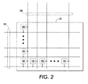
- FIG. 2 is a block diagram illustrating details of a sensor array according to an example embodiment
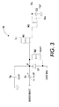
- FIG. 3 is , a schematic diagram illustrating an active pixel circuit according to an example embodiment
- FIGS. 4 and 5 are graphs illustrating results of a SPICE simulation of a pixel configured as shown in FIG. 3 ;
- FIG. 6 is a sample fingerprint image obtained from a capacitive touch pattern sensor according to an example embodiment
- FIG. 7 is a histogram of measured signal-to-noise active pixels of a capacitive sensing device according to an example embodiment.
- FIGS. 8 and 9 are flowcharts illustrating procedures according to example embodiments.
- the present disclosure relates to touch/proximity pattern sensors such as fingerprint sensors.
- finger prints and similar patterns, e.g., on hands and feet
- biometric indicators that are unique to each person.
- computer scanned hand/finger print images can be used for purposes such as authentication.
- a scanning sensor may include a flat surface against which to place the finger (or any scanned object). In response to the contact, the sensor generates an image of the texture/contours of the scanned object.
- Pattern recognition software can compare metrics of the scanned image to stored metrics, and confirm identity based on a match of the metrics.
- a fingerprint image can be obtained, such as using optical sensors.
- Embodiments described below use capacitive sensing.
- an object that touches a sensing surface will affect the local electric capacitance of the surface wherever there is contact.
- capacitive touch input sensing is widely used to determine coarse indications of contact location (e.g., touchscreens, touchpads)
- the sensors described herein may be capable of much higher resolution (e.g., on the order of 500 dpi) than a conventional touch input sensor.
- devices such as non-destructive testing imagers may obtain an image based on portions of an object that touch and/or are in relatively close proximity to a contact sensing element.
- FIG. 1 a cross sectional view illustrates a capacitive touch pattern sensor according to an example embodiment.
- a sensor array 102 is built on top of a substrate 104 (e.g., glass).
- the sensor array 102 includes a plurality of active pixels 100, examples of which will be described further below.
- each pixel 100 is electrically coupled to sensing pads 106.
- the pads 106 are electrically conductive and covered by an insulator layer 108.
- the insulator layer 108 may be made from a protective coating polymer such as Parylene.
- a conductive object 109 contacting the insulating layer 108 changes a local capacitance at the pads 106, and this is detected by active pixels 100 that are coupled to the affected pads 106.
- a fingerprint ridge 112 will cause a capacitance to be measured at a pad 106 directly below the ridge 112 that is different than another pad 106 directly below fingerprint valley 110.
- the capacitance may vary not only based on contact versus non-contact, but may also vary depending on the relative proximity of non-contacting portions. For example, different fingerprint valleys may cause different capacitance due to different distances from a surface of the insulating layer 108.
- FIG. 2 a block diagram illustrates details of a sensor array 102 according to an example embodiment.
- the sensor array 102 includes a number of individual active pixel elements 100. Each of these elements 100 are associated with one of a row line 204 and a column line 206.
- each of the row lines 204 may be activated in sequence. Activating a row line 204 causes all elements 100 in the rows to become active (e.g., switching on an enabling transistor).
- each of the column lines (e.g., data lines) 206 is scanned to read the individual elements 100 in the currently activated row. Alternate methods of scanning the elements 100 are known in the art, and the embodiments need not be limited to what is shown in FIG. 2 .
- each column line 206 may involve applying to each column line 206 a first voltage level for a first period of time, and then switching to a second, lower voltage level for a second period of time.
- the first voltage level charges the currently read element 100
- the second voltage level causes a current flow via the column line that indicates a sensed capacitance of the element 100.
- the active pixel 100 is generally configured as a three transistor sensor, sometimes abbreviated as a 3T sensor pixel.
- the three transistors M1, M2, M3 in this diagram are n-type, low-temperature, polycrystalline silicon (Poly-Si) thin-film transistors (TFTs) although it may be possible to use other types of transistor devices such as metal oxide semiconductor, field-effect transistors (MOSFETs). However, TFTs may hold an advantage over MOSFET, such as cost and ease of manufacture.
- Transistor M2 is configured as a reset transistor in response to reset signal G n+1 .
- M2 When G n+1 is activated, M2 shorts out high frequency rectifying/detection diode D1, allowing sensing junction J1 to be tied to the biasing voltage of D1.
- the reset transistor M2 By tying the reset transistor M2 to the enable line of the following row (G n+1 ), the active pixels 100 can be reset without using a separate set of reset lines.
- M2 may be reset by another line, such as the preceding row enable (G n-1 ), a separate reset line, a data line Dn of an adjacent column, etc.
- the Cp component is a parasitic capacitor, having one end coupled to the sensing junction J1 and the other end at ground.
- the C f component models the sensed capacitance of the pads and insulating layer (see sensing pads 106 and insulating layer 108 in FIG. 1 ).
- the effective value of C f may vary from zero (or near zero) to some maximum value (in this example on the order of 10 fF) depending on whether or not an object (e.g., fingerprint ridge) is contacting the insulating layer.
- the sensed capacitance can be found based on a ratio of gate capacitance of M1 (C M1 ) and the sum of C f , C p , and C M1 .
- the M1 transistor is configured as a source follower having its gate tied to the sensing junction J1.
- the output of M1 is tied to data line Dn when enabling transistor M3 is switched on in response to enable signal Gn.
- the transistor M1 also acts as a charge pump to charge up capacitors C f and C p . This charging occurs during the operation cycle of the pixel 100, when M3 is enabled. In one embodiment, the operation cycle is between 50-70 ⁇ s.
- the charge accumulated on the gate of M1 during charging interval will be redistributed among Cp, Cf, and C M1 .
- the final voltage (V sense ) at the sensing junction J1 at the end of sensing interval becomes input of source follower M1, and the output of M1 at this interval can be read out on Dn.
- the difference ⁇ V between the V charge and V sense potentials can be expressed as ⁇ V is approximately proportional to C M1 /(C f + Cp+ C M1 ).
- the capacitance C f may be determined by measuring current flowing through Dn during the sensing interval.
- C M1 and Cp can vary from what is shown while still falling within the scope of the claimed invention.
- the capacitance value of C M1 and Cp can modified from what is shown to match a physical configuration that provides sensed capacitance C f .
- C f has been found to be on the order of 10 fF (between 1 fF and 100 fF) and so C M1 and Cp are selected to fall within a similar range.
- C M1 may be inherent in the TFT design, and so modification of C M1 may be achieved by modifying physical configuration/physical dimension and/or type of transistor used, or by the addition of electrical components (e.g., inline capacitor).
- p-channel transistors may be used in the circuit, e.g., by replacing the illustrated n-channel transistors with p-channel devices, and by reversing diode direction and voltage polarities.
- FIGS. 4 and 5 graphs illustrates results of a SPICE simulation of a pixel 100 configured as shown in FIG. 3 .
- Time period 406 represents an operation cycle of M1.
- Intervals 408 and 410 represent respective charging and readout intervals within the operational cycle 406.
- Voltages 412 and 414 are proportional to the different values of C f , and can be used as basis for a detection signal, e.g., data line current out of the pixel 100.
- a detection signal e.g., data line current out of the pixel 100.
- the respective intervals 408, 410 are also shown in FIG. 5 , and the different in current during sensing interval 410 can be used to determine sensed capacitance.
- the potential difference applied to the data line between charging and readout intervals 408 and 410 can be provided by what is known as a data line reset switch.
- the data line reset switch includes TFTs located at the end of each data line, on the same substrate of pixel array.
- the TFTs are activated by a control line shared by all data line reset TFTs.
- the data line reset switches When the data line reset switches are activated, they connect the data lines to an external voltage source and set the data line potential to the value defined by the voltage source.
- V ref of readout charge amplifiers (coupled to readout lines 206 in FIG. 2 ) can be varied while a pixel is currently activated.
- TFT thin-film transistor
- SNR signal-to-noise ratio
- a histogram shows measured SNR for an active pixel capacitive sensing device according to an example embodiment.
- Curve 702 represents bright field SNR for a pixel array and curve 704 represents dark field SNR measurements for the same array.
- the peak of curve 702 is at 183, and the peak of curve 704 is 310.
- the gate capacitance C M1 is on the order of 10 fF (e.g., between 1fF and 100 fF), which is comparable (e.g., same order of magnitude) to the plate capacitance across the insulator, modeled in FIG. 3 as C f , and the value of the parasitic capacitor C p .
- These low capacitances make the circuit very sensitive to changes in C f . This, combined with the signal amplification provided by M2, provides superior sensitivity as reflected in the SNR measurements shown above.
- FIG. 8 a flowchart illustrates a method according to an example embodiment.
- the method involves activating 802 an enabling transistor in series with a source follower of a 3T sensor of an active pixel in a sensor array.
- a first voltage level is applied 804 to a data line of the 3T sensor.
- a second voltage is then applied 806 to the data line.
- a current flowing at the data line in response to the second voltage being applied is determined 808.
- a variable capacitance of an insulator layer over the active pixel may be determined 810 based on the current, and an image of an object proximate the insulator layer may be determined 812 based on the variable capacitance.
- FIG. 9 a flowchart illustrates a method according to an example embodiment.
- the method involves repeatedly performing operations 904-907, as indicated by loop entry block 902.
- the loop is performed for each of a plurality of active pixels of a capacitive touch sensor, e.g., via scanning some or all row and column lines of an array as shown in FIG. 2 .
- an enable transistor of a 3T sensor of the active pixel is enabled 904, and may remain enabled at least during subsequent steps 905-907.
- a first voltage level is applied 905 to a data line of the active pixel.
- the 3T sensor has a source follower transistor coupled to the data line (e.g., via the enable transistor) with a gate coupled to a sensing junction.
- a detection diode is coupled in series to a parasitic capacitor at the sensing junction.
- a second voltage is applied 906 to the data line.
- a variable capacitance of an insulator layer over the active pixel is determined 907 based on a current flowing at the data line in response to the second voltage being applied.
- a proximity image is determined 912 based on the variable capacitance measured from each of the plurality of active pixels.
Landscapes
- Engineering & Computer Science (AREA)
- General Engineering & Computer Science (AREA)
- Theoretical Computer Science (AREA)
- Physics & Mathematics (AREA)
- General Physics & Mathematics (AREA)
- Human Computer Interaction (AREA)
- Measurement Of Length, Angles, Or The Like Using Electric Or Magnetic Means (AREA)
- Transforming Light Signals Into Electric Signals (AREA)
- Solid State Image Pick-Up Elements (AREA)
- Image Input (AREA)
Applications Claiming Priority (1)
| Application Number | Priority Date | Filing Date | Title |
|---|---|---|---|
| US13/667,112 US8618865B1 (en) | 2012-11-02 | 2012-11-02 | Capacitive imaging device with active pixels |
Publications (3)
| Publication Number | Publication Date |
|---|---|
| EP2728512A2 true EP2728512A2 (de) | 2014-05-07 |
| EP2728512A3 EP2728512A3 (de) | 2015-07-01 |
| EP2728512B1 EP2728512B1 (de) | 2018-08-08 |
Family
ID=49679289
Family Applications (1)
| Application Number | Title | Priority Date | Filing Date |
|---|---|---|---|
| EP13191016.8A Not-in-force EP2728512B1 (de) | 2012-11-02 | 2013-10-31 | Kapazitative Bilderfassungsvorrichtung mit aktiven Pixeln |
Country Status (3)
| Country | Link |
|---|---|
| US (2) | US8618865B1 (de) |
| EP (1) | EP2728512B1 (de) |
| JP (1) | JP6190689B2 (de) |
Cited By (2)
| Publication number | Priority date | Publication date | Assignee | Title |
|---|---|---|---|---|
| CN105355171A (zh) * | 2015-12-15 | 2016-02-24 | 惠州Tcl移动通信有限公司 | 驱动扫描电路、显示屏及移动终端 |
| US10495911B2 (en) | 2015-10-09 | 2019-12-03 | Xiaomi Inc. | Liquid crystal display assembly and electronic device |
Families Citing this family (16)
| Publication number | Priority date | Publication date | Assignee | Title |
|---|---|---|---|---|
| JP6133904B2 (ja) * | 2012-02-06 | 2017-05-24 | クアルコム,インコーポレイテッド | 電界デバイスを使用するシステムおよび方法 |
| US8618865B1 (en) | 2012-11-02 | 2013-12-31 | Palo Alto Research Center Incorporated | Capacitive imaging device with active pixels |
| US9678591B2 (en) * | 2013-06-10 | 2017-06-13 | The Board Of Trustees Of The Leland Stanford Junior University | Method and apparatus for sensing touch |
| CN104866803B (zh) | 2014-02-20 | 2018-06-05 | 上海思立微电子科技有限公司 | 一种指纹信息检测电路 |
| US10101373B2 (en) | 2014-04-21 | 2018-10-16 | Palo Alto Research Center Incorporated | Capacitive imaging device with active pixels and method |
| US9215392B2 (en) | 2014-04-21 | 2015-12-15 | Palo Alto Research Center Incorporated | Impedance readout circuit and method having filter for determining an AC current component inversely proportional to the output impedance of a pixel |
| CN104103239B (zh) * | 2014-06-23 | 2016-05-04 | 京东方科技集团股份有限公司 | 有机发光二极管像素电路及其驱动方法 |
| CN104155785B (zh) * | 2014-08-07 | 2016-10-05 | 京东方科技集团股份有限公司 | 阵列基板及其驱动方法、显示装置 |
| CN104282265B (zh) | 2014-09-26 | 2017-02-01 | 京东方科技集团股份有限公司 | 像素电路及其驱动方法、有机发光显示面板及显示装置 |
| CN104516716A (zh) * | 2015-01-13 | 2015-04-15 | 深圳市亚耕电子科技有限公司 | 电子设备及其电容式感测系统、以及电容式感测系统的检测方法 |
| CN104866834B (zh) * | 2015-05-29 | 2018-08-10 | 上海箩箕技术有限公司 | 电容式指纹传感器和指纹成像模组 |
| US10325131B2 (en) * | 2015-06-30 | 2019-06-18 | Synaptics Incorporated | Active matrix capacitive fingerprint sensor for display integration based on charge sensing by a 2-TFT pixel architecture |
| US11692853B2 (en) * | 2016-01-06 | 2023-07-04 | Disruptive Technologies Research As | Ultra low power source follower for capacitive sensor shield drivers |
| KR20170102668A (ko) | 2016-03-02 | 2017-09-12 | 삼성전자주식회사 | 지문 감지 센서, 이를 포함하는 전자 장치 및 지문 감지 센서의 동작 방법 |
| KR101770521B1 (ko) * | 2016-08-26 | 2017-09-05 | 한양대학교 산학협력단 | 정전용량 인셀 터치 패널 및 이에 있어서 리드아웃 방법 |
| KR102773244B1 (ko) * | 2017-01-24 | 2025-02-28 | 삼성디스플레이 주식회사 | 터치 센서 및 이를 포함하는 표시 장치 |
Family Cites Families (76)
| Publication number | Priority date | Publication date | Assignee | Title |
|---|---|---|---|---|
| US4112365A (en) * | 1977-02-15 | 1978-09-05 | Eaton Corporation | Position detecting system |
| US4254345A (en) | 1979-05-21 | 1981-03-03 | Itt Industries, Inc. | Output circuit for bucket-brigade devices |
| US4323846A (en) | 1979-06-21 | 1982-04-06 | Rockwell International Corporation | Radiation hardened MOS voltage generator circuit |
| US4359756A (en) | 1981-06-29 | 1982-11-16 | Rca Corporation | Chrominance signal limiter |
| US5083016A (en) * | 1990-03-27 | 1992-01-21 | Hughes Aircraft Company | 3-transistor source follower-per-detector unit cell for 2-dimensional focal plane arrays |
| GB2244164A (en) | 1990-05-18 | 1991-11-20 | Philips Electronic Associated | Fingerprint sensing |
| US6201270B1 (en) * | 1997-04-07 | 2001-03-13 | Pao-Jung Chen | High speed CMOS photodetectors with wide range operating region and fixed pattern noise reduction |
| US5940526A (en) | 1997-05-16 | 1999-08-17 | Harris Corporation | Electric field fingerprint sensor having enhanced features and related methods |
| US6191593B1 (en) | 1997-12-17 | 2001-02-20 | Stmicroelectronics, Inc. | Method for the non-invasive sensing of physical matter on the detection surface of a capacitive sensor |
| US6410899B1 (en) * | 1998-06-17 | 2002-06-25 | Foveon, Inc. | Active pixel sensor with bootstrap amplification and reduced leakage during readout |
| US6246043B1 (en) * | 1998-09-22 | 2001-06-12 | Foveon, Inc. | Method and apparatus for biasing a CMOS active pixel sensor above the nominal voltage maximums for an IC process |
| JP2000213908A (ja) * | 1998-11-16 | 2000-08-04 | Sony Corp | 静電容量検出装置およびその検査方法並びに指紋照合装置 |
| DE19917863C1 (de) | 1999-04-20 | 2001-01-25 | Fraunhofer Ges Forschung | Schaltung zum Verarbeiten eines Analogsignals und Bildsensor |
| JP3469143B2 (ja) | 1999-11-02 | 2003-11-25 | シャープ株式会社 | アクティブマトリクス基板及びそれを備えた二次元画像検出器 |
| GB0108309D0 (en) * | 2001-04-03 | 2001-05-23 | Koninkl Philips Electronics Nv | Matrix array devices with flexible substrates |
| JP4225777B2 (ja) | 2002-02-08 | 2009-02-18 | シャープ株式会社 | 表示装置ならびにその駆動回路および駆動方法 |
| TW583592B (en) * | 2002-04-03 | 2004-04-11 | Lightuning Tech Inc | Capacitive fingerprint sensor |
| US7006078B2 (en) * | 2002-05-07 | 2006-02-28 | Mcquint, Inc. | Apparatus and method for sensing the degree and touch strength of a human body on a sensor |
| US7623169B2 (en) | 2002-06-26 | 2009-11-24 | Xerox Corporation | Low noise charge gain hybrid imager |
| US20090224351A1 (en) * | 2002-08-27 | 2009-09-10 | E-Phocus, Inc | CMOS sensor with approximately equal potential photodiodes |
| KR100574891B1 (ko) * | 2003-01-13 | 2006-04-27 | 매그나칩 반도체 유한회사 | 클램프 회로를 갖는 이미지센서 |
| FR2855326B1 (fr) * | 2003-05-23 | 2005-07-22 | Atmel Grenoble Sa | Capteur d'image matriciel en technologie cmos |
| US6906529B2 (en) | 2003-06-10 | 2005-06-14 | Stmicroelectronics, Inc. | Capacitive sensor device with electrically configurable pixels |
| US7616786B2 (en) | 2003-09-24 | 2009-11-10 | Authentec, Inc. | Finger biometric sensor with sensor electronics distributed over thin film and monocrystalline substrates and related methods |
| US20050079386A1 (en) | 2003-10-01 | 2005-04-14 | Board Of Regents, The University Of Texas System | Compositions, methods and systems for making and using electronic paper |
| US20080297878A1 (en) | 2003-10-01 | 2008-12-04 | Board Of Regents, The University Of Texas System | Compositions, methods and systems for making and using electronic paper |
| US20050094855A1 (en) | 2003-10-29 | 2005-05-05 | Proano Cesar H. | Fingerprint imaging using a flat panel detector |
| KR100970958B1 (ko) | 2003-11-04 | 2010-07-20 | 삼성전자주식회사 | 터치 스크린 기능을 갖는 액정 표시 장치 및 그의 제조 방법 |
| EP1583150A1 (de) * | 2004-03-31 | 2005-10-05 | CSEM Centre Suisse d'Electronique et de Microtechnique SA | Bildsensor mit grossflächigen, hochgeschwindigen, hochempfindlichen Pixeln |
| US8447077B2 (en) | 2006-09-11 | 2013-05-21 | Validity Sensors, Inc. | Method and apparatus for fingerprint motion tracking using an in-line array |
| FR2869723A1 (fr) * | 2004-04-29 | 2005-11-04 | Thomson Licensing Sa | Element de transition sans contact entre un guide d'ondes et une ligne mocroruban |
| EP1624490B1 (de) * | 2004-08-04 | 2018-10-03 | Heptagon Micro Optics Pte. Ltd. | Grossflächiger Pixel für die Verwendung in einem Bildsensor |
| WO2006042144A2 (en) | 2004-10-07 | 2006-04-20 | Ultra-Scan Corporation | Ultrasonic fingerprint scanning utilizing a plane wave |
| KR100552451B1 (ko) * | 2005-07-27 | 2006-02-21 | 실리콘 디스플레이 (주) | 문턱전압이 보상되는 요철 검출장치 및 그 방법 |
| KR100877691B1 (ko) * | 2005-12-08 | 2009-01-09 | 한국전자통신연구원 | 이미지 센서 및 이미지 센서의 트랜스퍼 트랜지스터 구동방법 |
| US8144115B2 (en) | 2006-03-17 | 2012-03-27 | Konicek Jeffrey C | Flat panel display screen operable for touch position determination system and methods |
| KR101128543B1 (ko) * | 2006-06-09 | 2012-03-23 | 애플 인크. | 터치 스크린 액정 디스플레이 |
| GB2446821A (en) | 2007-02-07 | 2008-08-27 | Sharp Kk | An ambient light sensing system |
| US7642498B2 (en) | 2007-04-04 | 2010-01-05 | Aptina Imaging Corporation | Capacitor multipler circuits and the applications thereof to attenuate row-wise temporal noise in image sensors |
| US7923801B2 (en) | 2007-04-18 | 2011-04-12 | Invisage Technologies, Inc. | Materials, systems and methods for optoelectronic devices |
| KR100851494B1 (ko) * | 2007-05-14 | 2008-08-08 | 매그나칩 반도체 유한회사 | 수직적으로 집적된 세트 및 리셋 다이오드를 갖는 cmos이미지 센서를 위한 소형 픽셀 |
| KR100851495B1 (ko) * | 2007-05-14 | 2008-08-08 | 매그나칩 반도체 유한회사 | Jfet 및 수직적으로 집적된 리셋 다이오드를 갖는이미지 센서의 소형 픽셀 |
| FR2918747A1 (fr) * | 2007-07-12 | 2009-01-16 | St Microelectronics Sa | Microcapteur de pression |
| KR100883026B1 (ko) * | 2007-12-27 | 2009-02-12 | 주식회사 동부하이텍 | 이미지센서 및 그 제조방법 |
| US7755369B2 (en) | 2008-02-20 | 2010-07-13 | Himax Technologies Limited | Capacitive fingerprint sensor and the panel thereof |
| US20090224343A1 (en) * | 2008-03-06 | 2009-09-10 | Micron Technology, Inc. | Methods of forming imager devices, imager devices configured for back side illumination, and systems including the same |
| KR100955339B1 (ko) | 2008-04-22 | 2010-04-29 | 주식회사 애트랩 | 접촉 및 접근을 감지할 수 있는 디스플레이 패널과디스플레이 장치 및 이 패널을 이용하는 접촉 및 접근 감지방법 |
| US8080775B2 (en) * | 2008-06-30 | 2011-12-20 | Raytheon Company | Differential source follower source leader addressable node readout circuit |
| TW201013495A (en) * | 2008-09-30 | 2010-04-01 | Hannstar Display Corp | In-cell capacitive type sensing input display device |
| US8384180B2 (en) | 2009-01-22 | 2013-02-26 | Palo Alto Research Center Incorporated | Gated co-planar poly-silicon thin film diode |
| JP5257104B2 (ja) * | 2009-01-30 | 2013-08-07 | カシオ計算機株式会社 | 表示装置 |
| US8217913B2 (en) | 2009-02-02 | 2012-07-10 | Apple Inc. | Integrated touch screen |
| KR101715013B1 (ko) | 2009-05-13 | 2017-03-10 | 시냅틱스 인코포레이티드 | 커패시티브 센서 디바이스 |
| WO2011001874A1 (ja) * | 2009-06-30 | 2011-01-06 | シャープ株式会社 | センサ回路及び表示装置 |
| JP2011015158A (ja) | 2009-07-01 | 2011-01-20 | Toshiba Corp | 固体撮像装置 |
| JP5222240B2 (ja) * | 2009-07-09 | 2013-06-26 | 株式会社ジャパンディスプレイイースト | 光センサ回路、および光センサアレイ |
| GB2475055A (en) * | 2009-11-03 | 2011-05-11 | Sharp Kk | Touch sensor circuits with pre-charging input |
| KR101688523B1 (ko) | 2010-02-24 | 2016-12-21 | 삼성전자주식회사 | 적층형 이미지 센서 |
| US9128281B2 (en) | 2010-09-14 | 2015-09-08 | Microsoft Technology Licensing, Llc | Eyepiece with uniformly illuminated reflective display |
| US8201739B2 (en) | 2010-03-08 | 2012-06-19 | Ultra-Scan Corporation | Biometric sensor with delay layer |
| WO2012048263A1 (en) | 2010-10-08 | 2012-04-12 | Authentec, Inc. | Finger sensing device including differential measurement circuitry and related methods |
| US9158958B2 (en) | 2010-10-28 | 2015-10-13 | Synaptics Incorporated | Signal strength enhancement in a biometric sensor array |
| US9259961B2 (en) | 2010-12-10 | 2016-02-16 | Palo Alto Research Center Incorporated | Large-area ultrasound contact imaging |
| US8539837B2 (en) * | 2010-12-10 | 2013-09-24 | Palo Alto Research Center Incorporated | Ultrasonic imaging using thin film transistor backplane |
| TWI456990B (zh) | 2011-04-08 | 2014-10-11 | 原相科技股份有限公司 | 高動態範圍影像感測電路及高動態範圍影像讀取方法 |
| US9160331B2 (en) | 2011-10-28 | 2015-10-13 | Atmel Corporation | Capacitive and inductive sensing |
| JP6077280B2 (ja) | 2011-11-29 | 2017-02-08 | 株式会社半導体エネルギー研究所 | 表示装置及び電子機器 |
| CN104169850B (zh) | 2012-01-12 | 2017-06-06 | 辛纳普蒂克斯公司 | 单层电容性成像传感器 |
| JP6133904B2 (ja) * | 2012-02-06 | 2017-05-24 | クアルコム,インコーポレイテッド | 電界デバイスを使用するシステムおよび方法 |
| US9176597B2 (en) | 2012-07-02 | 2015-11-03 | Stmicroelectronics Asia Pacific Pte Ltd | Directional capacitive proximity sensor with bootstrapping |
| US9214911B2 (en) | 2012-08-30 | 2015-12-15 | Infineon Technologies Ag | System and method for adjusting the sensitivity of a capacitive signal source |
| US8618865B1 (en) | 2012-11-02 | 2013-12-31 | Palo Alto Research Center Incorporated | Capacitive imaging device with active pixels |
| US9035906B2 (en) | 2013-03-13 | 2015-05-19 | Synaptics Incorporated | Proximity sensing |
| US20140266262A1 (en) | 2013-03-14 | 2014-09-18 | Perkinelmer Holdings, Inc. | High resolution fingerprint imaging device |
| US20150091842A1 (en) | 2013-09-30 | 2015-04-02 | Synaptics Incorporated | Matrix sensor for image touch sensing |
| US9081457B2 (en) | 2013-10-30 | 2015-07-14 | Synaptics Incorporated | Single-layer muti-touch capacitive imaging sensor |
-
2012
- 2012-11-02 US US13/667,112 patent/US8618865B1/en not_active Expired - Fee Related
-
2013
- 2013-10-18 JP JP2013217037A patent/JP6190689B2/ja not_active Expired - Fee Related
- 2013-10-31 EP EP13191016.8A patent/EP2728512B1/de not_active Not-in-force
- 2013-12-23 US US14/139,129 patent/US9964575B2/en not_active Expired - Fee Related
Non-Patent Citations (1)
| Title |
|---|
| None |
Cited By (2)
| Publication number | Priority date | Publication date | Assignee | Title |
|---|---|---|---|---|
| US10495911B2 (en) | 2015-10-09 | 2019-12-03 | Xiaomi Inc. | Liquid crystal display assembly and electronic device |
| CN105355171A (zh) * | 2015-12-15 | 2016-02-24 | 惠州Tcl移动通信有限公司 | 驱动扫描电路、显示屏及移动终端 |
Also Published As
| Publication number | Publication date |
|---|---|
| US20140159746A1 (en) | 2014-06-12 |
| EP2728512A3 (de) | 2015-07-01 |
| JP2014093774A (ja) | 2014-05-19 |
| US9964575B2 (en) | 2018-05-08 |
| JP6190689B2 (ja) | 2017-08-30 |
| US8618865B1 (en) | 2013-12-31 |
| EP2728512B1 (de) | 2018-08-08 |
Similar Documents
| Publication | Publication Date | Title |
|---|---|---|
| US8618865B1 (en) | Capacitive imaging device with active pixels | |
| KR101773031B1 (ko) | 향상된 감지소자를 갖는 정전용량 지문센서 | |
| Tartagni et al. | A fingerprint sensor based on the feedback capacitive sensing scheme | |
| KR101875052B1 (ko) | 감지소자로부터의 전류 판독에 따른 정전용량식 지문감지장치 | |
| JP2000514227A (ja) | 指紋感知装置及びこれを組み込んだシステム | |
| US9619689B2 (en) | System and method of using an electric field device | |
| KR100371115B1 (ko) | 요철 검출 센서, 지문 조합 장치 및 개인 판별 장치 | |
| TW202101188A (zh) | 高解析觸碰感應裝置及方法 | |
| KR102712497B1 (ko) | 에지 보정 구조를 갖는 지문 감지 장치 | |
| CN107683482B (zh) | 电容式指纹传感器 | |
| US10101373B2 (en) | Capacitive imaging device with active pixels and method | |
| CN109690560B (zh) | 具有不同电容式配置的指纹感测 | |
| US20130214801A1 (en) | Pressure-based Fingerprint Authentication Device | |
| KR100417726B1 (ko) | 이미지의 용량성 검출 방법 및 장치 | |
| US12322203B2 (en) | Biometric skin contact sensor and methods of operating a biometric skin contact sensor | |
| US12100238B2 (en) | Biometric skin contact sensor and methods of operating a biometric skin contact sensor | |
| US12125307B2 (en) | Biometric skin contact sensor and methods of operating a biometric skin contact sensor | |
| US12032669B2 (en) | Biometric skin contact sensing apparatus and method | |
| KR20160109258A (ko) | 지문 검출 장치 및 이의 구동 방법 | |
| JP2000279397A (ja) | 凹凸検出センサ、凹凸検出装置、指紋照合装置および個人判別装置 | |
| CN108475333B (zh) | 确定手指的物理特性的手指感测系统、方法和电子设备 | |
| GB2628120A (en) | Sensor and method | |
| KR101922516B1 (ko) | 디스플레이 영역에서의 생체 이미지 판독 장치 | |
| KR101913650B1 (ko) | 디스플레이 영역에서의 생체 이미지 판독 장치 | |
| KR20000019785A (ko) | 캐패시터 배열 구조를 이용한 2차원적 이미지 감지 장치 |
Legal Events
| Date | Code | Title | Description |
|---|---|---|---|
| PUAI | Public reference made under article 153(3) epc to a published international application that has entered the european phase |
Free format text: ORIGINAL CODE: 0009012 |
|
| 17P | Request for examination filed |
Effective date: 20131031 |
|
| AK | Designated contracting states |
Kind code of ref document: A2 Designated state(s): AL AT BE BG CH CY CZ DE DK EE ES FI FR GB GR HR HU IE IS IT LI LT LU LV MC MK MT NL NO PL PT RO RS SE SI SK SM TR |
|
| AX | Request for extension of the european patent |
Extension state: BA ME |
|
| REG | Reference to a national code |
Ref country code: DE Ref legal event code: R079 Ref document number: 602013041525 Country of ref document: DE Free format text: PREVIOUS MAIN CLASS: G06K0009200000 Ipc: G06K0009000000 |
|
| PUAL | Search report despatched |
Free format text: ORIGINAL CODE: 0009013 |
|
| AK | Designated contracting states |
Kind code of ref document: A3 Designated state(s): AL AT BE BG CH CY CZ DE DK EE ES FI FR GB GR HR HU IE IS IT LI LT LU LV MC MK MT NL NO PL PT RO RS SE SI SK SM TR |
|
| AX | Request for extension of the european patent |
Extension state: BA ME |
|
| RIC1 | Information provided on ipc code assigned before grant |
Ipc: G06K 9/00 20060101AFI20150527BHEP Ipc: G06F 3/044 20060101ALI20150527BHEP |
|
| 17P | Request for examination filed |
Effective date: 20151217 |
|
| RBV | Designated contracting states (corrected) |
Designated state(s): AL AT BE BG CH CY CZ DE DK EE ES FI FR GB GR HR HU IE IS IT LI LT LU LV MC MK MT NL NO PL PT RO RS SE SI SK SM TR |
|
| 17Q | First examination report despatched |
Effective date: 20160412 |
|
| GRAP | Despatch of communication of intention to grant a patent |
Free format text: ORIGINAL CODE: EPIDOSNIGR1 |
|
| INTG | Intention to grant announced |
Effective date: 20180228 |
|
| RIN1 | Information on inventor provided before grant (corrected) |
Inventor name: LU, JENG PING |
|
| GRAS | Grant fee paid |
Free format text: ORIGINAL CODE: EPIDOSNIGR3 |
|
| GRAA | (expected) grant |
Free format text: ORIGINAL CODE: 0009210 |
|
| AK | Designated contracting states |
Kind code of ref document: B1 Designated state(s): AL AT BE BG CH CY CZ DE DK EE ES FI FR GB GR HR HU IE IS IT LI LT LU LV MC MK MT NL NO PL PT RO RS SE SI SK SM TR |
|
| REG | Reference to a national code |
Ref country code: GB Ref legal event code: FG4D |
|
| REG | Reference to a national code |
Ref country code: CH Ref legal event code: EP Ref country code: AT Ref legal event code: REF Ref document number: 1027858 Country of ref document: AT Kind code of ref document: T Effective date: 20180815 |
|
| REG | Reference to a national code |
Ref country code: IE Ref legal event code: FG4D |
|
| REG | Reference to a national code |
Ref country code: DE Ref legal event code: R096 Ref document number: 602013041525 Country of ref document: DE |
|
| REG | Reference to a national code |
Ref country code: FR Ref legal event code: PLFP Year of fee payment: 6 |
|
| REG | Reference to a national code |
Ref country code: NL Ref legal event code: MP Effective date: 20180808 |
|
| REG | Reference to a national code |
Ref country code: LT Ref legal event code: MG4D |
|
| REG | Reference to a national code |
Ref country code: AT Ref legal event code: MK05 Ref document number: 1027858 Country of ref document: AT Kind code of ref document: T Effective date: 20180808 |
|
| PG25 | Lapsed in a contracting state [announced via postgrant information from national office to epo] |
Ref country code: RS Free format text: LAPSE BECAUSE OF FAILURE TO SUBMIT A TRANSLATION OF THE DESCRIPTION OR TO PAY THE FEE WITHIN THE PRESCRIBED TIME-LIMIT Effective date: 20180808 Ref country code: LT Free format text: LAPSE BECAUSE OF FAILURE TO SUBMIT A TRANSLATION OF THE DESCRIPTION OR TO PAY THE FEE WITHIN THE PRESCRIBED TIME-LIMIT Effective date: 20180808 Ref country code: SE Free format text: LAPSE BECAUSE OF FAILURE TO SUBMIT A TRANSLATION OF THE DESCRIPTION OR TO PAY THE FEE WITHIN THE PRESCRIBED TIME-LIMIT Effective date: 20180808 Ref country code: BG Free format text: LAPSE BECAUSE OF FAILURE TO SUBMIT A TRANSLATION OF THE DESCRIPTION OR TO PAY THE FEE WITHIN THE PRESCRIBED TIME-LIMIT Effective date: 20181108 Ref country code: NL Free format text: LAPSE BECAUSE OF FAILURE TO SUBMIT A TRANSLATION OF THE DESCRIPTION OR TO PAY THE FEE WITHIN THE PRESCRIBED TIME-LIMIT Effective date: 20180808 Ref country code: FI Free format text: LAPSE BECAUSE OF FAILURE TO SUBMIT A TRANSLATION OF THE DESCRIPTION OR TO PAY THE FEE WITHIN THE PRESCRIBED TIME-LIMIT Effective date: 20180808 Ref country code: GR Free format text: LAPSE BECAUSE OF FAILURE TO SUBMIT A TRANSLATION OF THE DESCRIPTION OR TO PAY THE FEE WITHIN THE PRESCRIBED TIME-LIMIT Effective date: 20181109 Ref country code: NO Free format text: LAPSE BECAUSE OF FAILURE TO SUBMIT A TRANSLATION OF THE DESCRIPTION OR TO PAY THE FEE WITHIN THE PRESCRIBED TIME-LIMIT Effective date: 20181108 Ref country code: AT Free format text: LAPSE BECAUSE OF FAILURE TO SUBMIT A TRANSLATION OF THE DESCRIPTION OR TO PAY THE FEE WITHIN THE PRESCRIBED TIME-LIMIT Effective date: 20180808 Ref country code: IS Free format text: LAPSE BECAUSE OF FAILURE TO SUBMIT A TRANSLATION OF THE DESCRIPTION OR TO PAY THE FEE WITHIN THE PRESCRIBED TIME-LIMIT Effective date: 20181208 Ref country code: PL Free format text: LAPSE BECAUSE OF FAILURE TO SUBMIT A TRANSLATION OF THE DESCRIPTION OR TO PAY THE FEE WITHIN THE PRESCRIBED TIME-LIMIT Effective date: 20180808 |
|
| PG25 | Lapsed in a contracting state [announced via postgrant information from national office to epo] |
Ref country code: LV Free format text: LAPSE BECAUSE OF FAILURE TO SUBMIT A TRANSLATION OF THE DESCRIPTION OR TO PAY THE FEE WITHIN THE PRESCRIBED TIME-LIMIT Effective date: 20180808 Ref country code: HR Free format text: LAPSE BECAUSE OF FAILURE TO SUBMIT A TRANSLATION OF THE DESCRIPTION OR TO PAY THE FEE WITHIN THE PRESCRIBED TIME-LIMIT Effective date: 20180808 Ref country code: AL Free format text: LAPSE BECAUSE OF FAILURE TO SUBMIT A TRANSLATION OF THE DESCRIPTION OR TO PAY THE FEE WITHIN THE PRESCRIBED TIME-LIMIT Effective date: 20180808 |
|
| PG25 | Lapsed in a contracting state [announced via postgrant information from national office to epo] |
Ref country code: IT Free format text: LAPSE BECAUSE OF FAILURE TO SUBMIT A TRANSLATION OF THE DESCRIPTION OR TO PAY THE FEE WITHIN THE PRESCRIBED TIME-LIMIT Effective date: 20180808 Ref country code: RO Free format text: LAPSE BECAUSE OF FAILURE TO SUBMIT A TRANSLATION OF THE DESCRIPTION OR TO PAY THE FEE WITHIN THE PRESCRIBED TIME-LIMIT Effective date: 20180808 Ref country code: CZ Free format text: LAPSE BECAUSE OF FAILURE TO SUBMIT A TRANSLATION OF THE DESCRIPTION OR TO PAY THE FEE WITHIN THE PRESCRIBED TIME-LIMIT Effective date: 20180808 Ref country code: ES Free format text: LAPSE BECAUSE OF FAILURE TO SUBMIT A TRANSLATION OF THE DESCRIPTION OR TO PAY THE FEE WITHIN THE PRESCRIBED TIME-LIMIT Effective date: 20180808 Ref country code: EE Free format text: LAPSE BECAUSE OF FAILURE TO SUBMIT A TRANSLATION OF THE DESCRIPTION OR TO PAY THE FEE WITHIN THE PRESCRIBED TIME-LIMIT Effective date: 20180808 |
|
| REG | Reference to a national code |
Ref country code: DE Ref legal event code: R097 Ref document number: 602013041525 Country of ref document: DE |
|
| PG25 | Lapsed in a contracting state [announced via postgrant information from national office to epo] |
Ref country code: SM Free format text: LAPSE BECAUSE OF FAILURE TO SUBMIT A TRANSLATION OF THE DESCRIPTION OR TO PAY THE FEE WITHIN THE PRESCRIBED TIME-LIMIT Effective date: 20180808 Ref country code: DK Free format text: LAPSE BECAUSE OF FAILURE TO SUBMIT A TRANSLATION OF THE DESCRIPTION OR TO PAY THE FEE WITHIN THE PRESCRIBED TIME-LIMIT Effective date: 20180808 Ref country code: SK Free format text: LAPSE BECAUSE OF FAILURE TO SUBMIT A TRANSLATION OF THE DESCRIPTION OR TO PAY THE FEE WITHIN THE PRESCRIBED TIME-LIMIT Effective date: 20180808 |
|
| REG | Reference to a national code |
Ref country code: CH Ref legal event code: PL |
|
| PLBE | No opposition filed within time limit |
Free format text: ORIGINAL CODE: 0009261 |
|
| STAA | Information on the status of an ep patent application or granted ep patent |
Free format text: STATUS: NO OPPOSITION FILED WITHIN TIME LIMIT |
|
| REG | Reference to a national code |
Ref country code: BE Ref legal event code: MM Effective date: 20181031 |
|
| PG25 | Lapsed in a contracting state [announced via postgrant information from national office to epo] |
Ref country code: MC Free format text: LAPSE BECAUSE OF FAILURE TO SUBMIT A TRANSLATION OF THE DESCRIPTION OR TO PAY THE FEE WITHIN THE PRESCRIBED TIME-LIMIT Effective date: 20180808 Ref country code: LU Free format text: LAPSE BECAUSE OF NON-PAYMENT OF DUE FEES Effective date: 20181031 |
|
| 26N | No opposition filed |
Effective date: 20190509 |
|
| REG | Reference to a national code |
Ref country code: IE Ref legal event code: MM4A |
|
| PG25 | Lapsed in a contracting state [announced via postgrant information from national office to epo] |
Ref country code: LI Free format text: LAPSE BECAUSE OF NON-PAYMENT OF DUE FEES Effective date: 20181031 Ref country code: CH Free format text: LAPSE BECAUSE OF NON-PAYMENT OF DUE FEES Effective date: 20181031 Ref country code: SI Free format text: LAPSE BECAUSE OF FAILURE TO SUBMIT A TRANSLATION OF THE DESCRIPTION OR TO PAY THE FEE WITHIN THE PRESCRIBED TIME-LIMIT Effective date: 20180808 Ref country code: BE Free format text: LAPSE BECAUSE OF NON-PAYMENT OF DUE FEES Effective date: 20181031 |
|
| PG25 | Lapsed in a contracting state [announced via postgrant information from national office to epo] |
Ref country code: IE Free format text: LAPSE BECAUSE OF NON-PAYMENT OF DUE FEES Effective date: 20181031 |
|
| PG25 | Lapsed in a contracting state [announced via postgrant information from national office to epo] |
Ref country code: MT Free format text: LAPSE BECAUSE OF NON-PAYMENT OF DUE FEES Effective date: 20181031 |
|
| PG25 | Lapsed in a contracting state [announced via postgrant information from national office to epo] |
Ref country code: TR Free format text: LAPSE BECAUSE OF FAILURE TO SUBMIT A TRANSLATION OF THE DESCRIPTION OR TO PAY THE FEE WITHIN THE PRESCRIBED TIME-LIMIT Effective date: 20180808 |
|
| PG25 | Lapsed in a contracting state [announced via postgrant information from national office to epo] |
Ref country code: PT Free format text: LAPSE BECAUSE OF FAILURE TO SUBMIT A TRANSLATION OF THE DESCRIPTION OR TO PAY THE FEE WITHIN THE PRESCRIBED TIME-LIMIT Effective date: 20180808 |
|
| PG25 | Lapsed in a contracting state [announced via postgrant information from national office to epo] |
Ref country code: HU Free format text: LAPSE BECAUSE OF FAILURE TO SUBMIT A TRANSLATION OF THE DESCRIPTION OR TO PAY THE FEE WITHIN THE PRESCRIBED TIME-LIMIT; INVALID AB INITIO Effective date: 20131031 Ref country code: CY Free format text: LAPSE BECAUSE OF FAILURE TO SUBMIT A TRANSLATION OF THE DESCRIPTION OR TO PAY THE FEE WITHIN THE PRESCRIBED TIME-LIMIT Effective date: 20180808 Ref country code: MK Free format text: LAPSE BECAUSE OF NON-PAYMENT OF DUE FEES Effective date: 20180808 |
|
| PGFP | Annual fee paid to national office [announced via postgrant information from national office to epo] |
Ref country code: FR Payment date: 20200917 Year of fee payment: 8 Ref country code: GB Payment date: 20200921 Year of fee payment: 8 |
|
| PGFP | Annual fee paid to national office [announced via postgrant information from national office to epo] |
Ref country code: DE Payment date: 20200917 Year of fee payment: 8 |
|
| REG | Reference to a national code |
Ref country code: DE Ref legal event code: R079 Ref document number: 602013041525 Country of ref document: DE Free format text: PREVIOUS MAIN CLASS: G06K0009000000 Ipc: G06V0010000000 |
|
| REG | Reference to a national code |
Ref country code: DE Ref legal event code: R119 Ref document number: 602013041525 Country of ref document: DE |
|
| GBPC | Gb: european patent ceased through non-payment of renewal fee |
Effective date: 20211031 |
|
| PG25 | Lapsed in a contracting state [announced via postgrant information from national office to epo] |
Ref country code: GB Free format text: LAPSE BECAUSE OF NON-PAYMENT OF DUE FEES Effective date: 20211031 Ref country code: DE Free format text: LAPSE BECAUSE OF NON-PAYMENT OF DUE FEES Effective date: 20220503 |
|
| PG25 | Lapsed in a contracting state [announced via postgrant information from national office to epo] |
Ref country code: FR Free format text: LAPSE BECAUSE OF NON-PAYMENT OF DUE FEES Effective date: 20211031 |