EP2726822B1 - Active shield for capacitive measurement system - Google Patents
Active shield for capacitive measurement system Download PDFInfo
- Publication number
- EP2726822B1 EP2726822B1 EP12730982.1A EP12730982A EP2726822B1 EP 2726822 B1 EP2726822 B1 EP 2726822B1 EP 12730982 A EP12730982 A EP 12730982A EP 2726822 B1 EP2726822 B1 EP 2726822B1
- Authority
- EP
- European Patent Office
- Prior art keywords
- sensor
- circuit
- current
- voltage
- measurement signal
- Prior art date
- Legal status (The legal status is an assumption and is not a legal conclusion. Google has not performed a legal analysis and makes no representation as to the accuracy of the status listed.)
- Active
Links
- 238000005259 measurement Methods 0.000 title claims description 144
- 239000004020 conductor Substances 0.000 claims description 74
- 238000001459 lithography Methods 0.000 claims description 23
- 239000010409 thin film Substances 0.000 claims description 15
- 238000005070 sampling Methods 0.000 claims description 12
- 238000001914 filtration Methods 0.000 claims description 4
- 238000000034 method Methods 0.000 claims description 3
- 238000010586 diagram Methods 0.000 description 23
- 239000000523 sample Substances 0.000 description 13
- 230000000694 effects Effects 0.000 description 10
- 238000012545 processing Methods 0.000 description 7
- 239000002245 particle Substances 0.000 description 6
- 208000006011 Stroke Diseases 0.000 description 4
- 239000003990 capacitor Substances 0.000 description 4
- 230000003071 parasitic effect Effects 0.000 description 4
- 230000035945 sensitivity Effects 0.000 description 4
- 238000010276 construction Methods 0.000 description 2
- 238000013016 damping Methods 0.000 description 2
- 238000005286 illumination Methods 0.000 description 2
- 238000012423 maintenance Methods 0.000 description 2
- 238000004519 manufacturing process Methods 0.000 description 2
- 238000000926 separation method Methods 0.000 description 2
- 239000000758 substrate Substances 0.000 description 2
- 238000012546 transfer Methods 0.000 description 2
- XUIMIQQOPSSXEZ-UHFFFAOYSA-N Silicon Chemical compound [Si] XUIMIQQOPSSXEZ-UHFFFAOYSA-N 0.000 description 1
- 230000002411 adverse Effects 0.000 description 1
- 238000013459 approach Methods 0.000 description 1
- 238000003491 array Methods 0.000 description 1
- 230000003139 buffering effect Effects 0.000 description 1
- 238000006243 chemical reaction Methods 0.000 description 1
- 239000000356 contaminant Substances 0.000 description 1
- 230000008878 coupling Effects 0.000 description 1
- 238000010168 coupling process Methods 0.000 description 1
- 238000005859 coupling reaction Methods 0.000 description 1
- 230000001419 dependent effect Effects 0.000 description 1
- 238000013461 design Methods 0.000 description 1
- 238000001514 detection method Methods 0.000 description 1
- 230000005684 electric field Effects 0.000 description 1
- 238000007689 inspection Methods 0.000 description 1
- 238000009434 installation Methods 0.000 description 1
- 238000002955 isolation Methods 0.000 description 1
- 229910000595 mu-metal Inorganic materials 0.000 description 1
- 230000003287 optical effect Effects 0.000 description 1
- 230000010363 phase shift Effects 0.000 description 1
- 238000000206 photolithography Methods 0.000 description 1
- 229910052710 silicon Inorganic materials 0.000 description 1
- 239000010703 silicon Substances 0.000 description 1
Images


Classifications
-
- G—PHYSICS
- G01—MEASURING; TESTING
- G01B—MEASURING LENGTH, THICKNESS OR SIMILAR LINEAR DIMENSIONS; MEASURING ANGLES; MEASURING AREAS; MEASURING IRREGULARITIES OF SURFACES OR CONTOURS
- G01B7/00—Measuring arrangements characterised by the use of electric or magnetic techniques
- G01B7/14—Measuring arrangements characterised by the use of electric or magnetic techniques for measuring distance or clearance between spaced objects or spaced apertures
-
- G—PHYSICS
- G01—MEASURING; TESTING
- G01D—MEASURING NOT SPECIALLY ADAPTED FOR A SPECIFIC VARIABLE; ARRANGEMENTS FOR MEASURING TWO OR MORE VARIABLES NOT COVERED IN A SINGLE OTHER SUBCLASS; TARIFF METERING APPARATUS; MEASURING OR TESTING NOT OTHERWISE PROVIDED FOR
- G01D5/00—Mechanical means for transferring the output of a sensing member; Means for converting the output of a sensing member to another variable where the form or nature of the sensing member does not constrain the means for converting; Transducers not specially adapted for a specific variable
- G01D5/12—Mechanical means for transferring the output of a sensing member; Means for converting the output of a sensing member to another variable where the form or nature of the sensing member does not constrain the means for converting; Transducers not specially adapted for a specific variable using electric or magnetic means
- G01D5/14—Mechanical means for transferring the output of a sensing member; Means for converting the output of a sensing member to another variable where the form or nature of the sensing member does not constrain the means for converting; Transducers not specially adapted for a specific variable using electric or magnetic means influencing the magnitude of a current or voltage
- G01D5/24—Mechanical means for transferring the output of a sensing member; Means for converting the output of a sensing member to another variable where the form or nature of the sensing member does not constrain the means for converting; Transducers not specially adapted for a specific variable using electric or magnetic means influencing the magnitude of a current or voltage by varying capacitance
- G01D5/2403—Mechanical means for transferring the output of a sensing member; Means for converting the output of a sensing member to another variable where the form or nature of the sensing member does not constrain the means for converting; Transducers not specially adapted for a specific variable using electric or magnetic means influencing the magnitude of a current or voltage by varying capacitance by moving plates, not forming part of the capacitor itself, e.g. shields
-
- G—PHYSICS
- G01—MEASURING; TESTING
- G01R—MEASURING ELECTRIC VARIABLES; MEASURING MAGNETIC VARIABLES
- G01R19/00—Arrangements for measuring currents or voltages or for indicating presence or sign thereof
- G01R19/0092—Arrangements for measuring currents or voltages or for indicating presence or sign thereof measuring current only
-
- G—PHYSICS
- G03—PHOTOGRAPHY; CINEMATOGRAPHY; ANALOGOUS TECHNIQUES USING WAVES OTHER THAN OPTICAL WAVES; ELECTROGRAPHY; HOLOGRAPHY
- G03F—PHOTOMECHANICAL PRODUCTION OF TEXTURED OR PATTERNED SURFACES, e.g. FOR PRINTING, FOR PROCESSING OF SEMICONDUCTOR DEVICES; MATERIALS THEREFOR; ORIGINALS THEREFOR; APPARATUS SPECIALLY ADAPTED THEREFOR
- G03F9/00—Registration or positioning of originals, masks, frames, photographic sheets or textured or patterned surfaces, e.g. automatically
- G03F9/70—Registration or positioning of originals, masks, frames, photographic sheets or textured or patterned surfaces, e.g. automatically for microlithography
- G03F9/7049—Technique, e.g. interferometric
- G03F9/7053—Non-optical, e.g. mechanical, capacitive, using an electron beam, acoustic or thermal waves
Definitions
- the present invention relates to a capacitive sensor for measuring distance, in particular capacitive sensor for measuring distance to a target in a lithography apparatus.
- Capacitive sensors may be used in such applications requiring fine position or distance measurement. When a capacitive sensor is energized, an electrical current flows through the sensor which varies in dependence on the distance between the sensor element and an opposing surface. A precise measurement of this current may be used to accurately determine the measured distance.
- a measurement circuit may be used having the current to be measured as the input and providing a measurement signal as an output, often in the form of a voltage which may be further processed and converted to a digital signal.
- CMRR common mode rejection ratio
- CMRR common mode rejection ratio
- the value of such stray impedance may change, e.g. depending on factors such as temperature, and disturbances on the input may also change with time. This makes it difficult to compensate for these effects.
- the electronic measurement circuits used for driving the capacitive sensors and for generating the desired measurement signals at a distance from the sensors due to the inhospitable environment in which the sensors are located or lack of a suitable place to locate the circuits close to the sensors.
- the sensors are typically located in a vacuum environment that is very sensitive to contaminants and outside disturbances, and which creates problems with heat removal from electronic circuits if they are located in the vacuum environment, and impedes access for maintenance for such circuits.
- the wiring connections between the sensors and remotely located driving and measurement circuits introduce parasitic capacitances into the system which affect the reading of the sensor. If the measuring circuits could be located at the sensor probe, the sensor current could be measured directly and accurately. Because of these parallel parasitic capacitances introduced by the cabling system, measurement of current flow in the sensor is often avoided in systems with remotely located measuring circuits. Conventional solutions introduce measurement errors which need to be taken into account, usually by calibrating the combined sensor and wiring installation. The longer the wiring connection, the more severe these problems become.
- Patent document US5489888 discloses a capacitance measuring system where the sensor head is remotely positioned from the associated drive and detection circuitry by means of a shielded cable, where the cable shield is energised by an amplifier to a potential so as to compensate for the intrinsic cable capacitance between the central sensing wire and the cable shield.
- the invention seeks to solve or reduce the above drawbacks to provide an improved capacitive measurement system for generating a measurement signal representative of a measured position or distance to a target.
- the system includes a first circuit comprising a thin film capacitive sensor arranged for providing a sensor capacitance in dependence on the measured position or distance; a cable comprising a sensor wire and a co-axial shield conductor, the cable having a remote end and a local end, the sensor wire electrically connected to the capacitive sensor at the local end of the cable; a voltage source having an output terminal connected to the sensor wire at the remote end of the cable and arranged to energize the capacitive sensor, and energize the shield conductor with essentially the same voltage as the sensor wire; and a current measuring circuit having first and second input terminals and an output terminal, the current measuring circuit connected in series with the first input terminal connected to the output terminal of the voltage source and the second input terminal connected to the sensor wire at the remote end of the cable, the current measuring circuit arranged to measure current flowing in the sensor wire and
- the configuration of the system provides for a low cost system able to generate very precise measurement of distances and positions.
- the use of a thin film construction for the sensor enables the use of low cost manufacturing techniques and avoids expensive precision manufacturing of conventional capacitive sensors.
- the use of a voltage source to energize the capacitive sensor instead of a more complex current source lowers the cost and complexity of the circuitry without sacrificing accuracy of the measurement.
- the configuration using a connecting cable with an active shield enables the electronic circuits (e.g. the voltage source and current measuring circuit to be located remotely from the sensor. This is significant as it is often difficult to have such electronic circuits close to the sensors due to lack of space at the sensor location or due to other limiting circumstances.
- the arrangement of the voltage source and current measuring circuit, and their connections to the cable and sensor provides a means to nullify the effects of the parasitic capacitances introduced by the cable system connecting the sensor and measuring circuit, in a simple arrangement which reduces or eliminates sources of measurement error found in conventional solutions. These factors result in a position/distance measurement system that can be applied in many situations to yield a low cost but precise measurement and control of position of the many moveable elements within a lithography or other type of complex system.
- the sensor wire and the shield conductor of the measurement system may be elements of a coaxial cable, the sensor wire comprising a core conductor of the coaxial cable and the shield conductor comprising an outer conductor of the coaxial cable.
- the coaxial cable may be a triaxial cable which further comprises a grounded outer shield conductor coaxial to and around the shield conductor.
- the measurement system may further comprise a second circuit comprising a second capacitive sensor, a second cable comprising a second sensor wire and a second shield conductor, a second voltage source, and a second current measuring circuit, the second circuit being arranged in the same way as the first circuit, wherein the voltage source and the second voltage source generate voltages 180 degrees out-of-phase to each other to energize the capacitive sensor and the second capacitive sensor in a differential pair arrangement.
- the voltage source of the measurement system may be configured to generate a triangular AC voltage waveform, and the voltage source may be further configured to generate a waveform having constant frequency, constant amplitude, and alternating positive and negative slope of constant slope.
- the measurement system may be configured so that the voltages supplied by the voltage source to the sensor wire and the shield conductor are essentially the same.
- the shield conductor may be directly connected to an output of the voltage source.
- the measurement system may be configured to drive the shield conductor, and couple the shield conductor to the sensor wire so that the voltage on the sensor wire follows the voltage on the shield conductor. This is the reverse of the conventional arrangement in which the sensor wire is driven and the voltage on the sensor wire is copied onto the shield conductor.
- the measurement system may further comprise a shield driver connected in series between the voltage source and the current measurement circuit.
- the output of the shield driver may be directed connected to the shield conductor to drive the sensor wire and the shield conductor with essentially the same voltage.
- the invention further provides a capacitive measurement system comprising a cable comprising a sensor wire for connection to a capacitive sensor, the cable also having a shield conductor; a voltage source for supplying a voltage for energizing the sensor wire and the shield conductor; a current measuring circuit connected in series between the voltage source and the sensor wire for measuring current flow in the sensor wire; and a shield driver connected in series between the voltage source and the current measuring circuit, the output of the shield driver being directly connected to the shield conductor; wherein the system is configured so that the shield driver drives the shield conductor directly and the sensor wire through the current measuring circuit.
- the invention comprises a capacitance measuring arrangement for use in the above system, the arrangement comprising a voltage source; a current measuring circuit having a first terminal connected to an output of the voltage source; a connection point for connecting a sensor wire of a sensor cable directly to a second terminal of the current measuring circuit; and a connection point for connecting a shield conductor of a sensor cable directly to the output of the voltage source.
- the invention includes a method for measuring a capacitance comprising connecting a capacitive sensor to a first end of a sensor wire; providing a shield conductor (32a) adapted for shielding the sensor wire from electrical disturbances; supplying an alternating voltage to a second end of the sensor wire and to the shield conductor; and measuring current flowing in the sensor wire.
- the invention provides a measurement circuit for processing a differential measurement signal comprising a first signal and a second inverted signal, the circuit comprising a first circuit for generating a plurality of phase offset reference signals; and a first sampling circuit for sampling the first signal during a first positive cycle and sampling the second inverted signal during a second positive cycle, to generate a first sample output.
- a first low pass filter may be provided for filtering the first sample output to generate a first measurement signal indicative of the peak amplitude of the differential measurement signal.
- the measurement circuit may additionally comprise a second sampling circuit for sampling the second inverted signal during a first negative cycle and sampling the first signal during a second negative cycle, to generate a second sample output.
- a second low pass filter may be provided for filtering the second sample output to generate a second measurement signal indicative of the peak amplitude of the differential measurement signal.
- the measurement circuit may include a circuit for subtracting the first measurement signal and the second measurement signal.
- the first sampling circuit may be configured to sample the differential measurement signal during an end portion of a cycle of the differential measurement signal.
- the invention also provides a lithography machine comprising a stage for carrying a wafer, a projection lens element, and a capacitive sensor configured for measuring a distance between the wafer and the projection lens element, the machine further comprising a capacitive sensing system as described above.
- the lithography machine may also include a measurement circuit as described above.
- a capacitive sensor uses a homogeneous electric field set up between two conductive surfaces. Over short distances, the applied voltage is proportional to the distance between the surfaces.
- Single-plate sensors measure the distance between a single sensor plate and an electrically conductive target surface.
- Fig. 1 shows a single capacitive sensor probe 1 measuring the position of or separation distance to grounded conductive target 2.
- current When supplied with an AC current, current will flow along a path 3 from the sensor to the target through the sensor-target capacitance 4, and from the target to ground through the target-ground impedance 5.
- the voltage across the sensor will vary in dependence on the distance separating the sensor probe and the surface of the target, and measuring this voltage will provide a measurement of target position or distance from the sensor probe to the target. The accuracy of the measurement depends on how accurately the sensor can measure the sensor-target capacitance 4.
- Fig. 2 shows an arrangement of two capacitive sensor probes 1a and 1b for a differential measurement of the position or separation distance to target 2.
- the sensors are supplied with an AC current with a phase offset of 180 degrees, so that current will flow along a path 6 from one sensor to the target through the sensor-target capacitance 4a, and from the target to the other sensor through the other sensor-target capacitance 4b.
- This arrangement for driving the two sensors with out-of-phase signals is effective to avoid flow of current through the target to ground, and minimizes the effect of the target to ground impedance. It is also useful for an ungrounded target as it allows current to flow from one sensor to the other without needing a grounded return path.
- the capacitive sensor may be energized by an AC voltage source or AC current source, and the resulting voltage across the sensor or current through the sensor is measured.
- the measurement signal generated is dependent on the sensor-to-target capacitance of the sensor.
- the system can be calibrated to the measurement capacitor and to measure the current/voltage.
- Fig. 3 is a diagram showing such a cable connection and the capacitances introduced by the cable into the sensor system.
- the sensor-to-target capacitance 4 is the capacitance to be measured (also referred to as the sensor capacitance), which depends on the distance between the sensor and the target.
- the cable 30 comprises a central conductor 31 and coaxial shield conductor 32, and the cable introduces stray capacitance 36, referred to as the cable capacitance, between the sensor wire 31 and shield 32, and stray ground capacitance 37 between the shield 32 and ground.
- a voltage source 20 is connected through a current measurement circuit 21 to one end of the sensor wire 31 and the measurement electrode of the capacitive sensor is connected to the other end of the sensor wire.
- the voltage source 20 supplies an AC voltage to energize the capacitive sensor 1, and the current measurement circuit 21 measures the current flowing in the sensor wire 31 through the capacitive sensor 1.
- the current flowing through the sensor wire 31 varies in dependence on the sensor capacitance 4, which varies in dependence on the distance being measured by the sensor.
- the current flowing in the sensor wire 31 will include a component due to current flowing through the sensor capacitance 4 and also a component due to current flowing through the cable capacitance 36.
- the cable capacitance 36 should be small in comparison to the sensor capacitance 4 because large stray capacitances increase the proportion of current flowing through the stray capacitances in comparison to the current flowing through the sensor capacitance desired to be measured, and reduces the sensitivity of the measurement.
- the cable capacitance is typically large and has an adverse effect on sensor system sensitivity.
- FIG. 3 shows a conventional arrangement with a shield driver 24 comprising a unitary gain amplifier/buffer with an input connected to the end of sensor wire 31 and an output connected to shield 32.
- the shield driver 24 energizes shield 32 with (essentially) the same voltage as present on sensor wire 31. Since the sensor wire 31 and shield conductor 32 have almost the same voltage on them, there is only a small voltage difference between them and only a small current flow through the cable capacitance 36, and the effect of cable capacitance 36 between the conductors is reduced.
- the gain of the shield driver only approaches a gain of 1.0 and some deviation in the gain must be expected.
- shield driver 24 Current flow through stray cable-to-ground capacitance 37 is supplied by shield driver 24.
- the input current to shield driver 24 will contribute to the current measured by current measurement circuit 21 resulting in error, but the shield driver has a high input impedance and its input current is relatively small so that the resulting error is small. However, for long cables and higher measurement frequencies this arrangement is difficult to realize.
- the shield driver also has some input capacitance, which will draw additional current.
- the measured capacitance is the sum of the sensor capacitance 4 and these additional error capacitances; the deviation from unit gain of the shield driver 24 multiplied by the stray capacitance 36, and the input capacitance of the shield driver 24.
- the measurement error can be reduced by rearranging the circuit as shown in Fig. 4 .
- This arrangement is for driving two capacitive sensors in a differential pair arrangement.
- a second sensor and second measurement circuit with an inverted driver may be used in a differential pair arrangement such as shown in Fig. 4 .
- the output of voltage source 20a is connected to the input of shield driver 24a, the output of shield driver 24a is connected to one terminal of current measurement circuit 21a, and the other terminal of measurement circuit 21a is connected to sensor wire 31a.
- the same arrangement is used for voltage source 20b, shield driver 24b, current measurement circuit 21b, and sensor wire 31b.
- the Voltage sources 20a and 20b generate AC voltage waveforms phase offset by 180 degrees to each other.
- the target conducts the alternating current between the two sensors 1a and 1b through the two sensor capacitances 4a and 4b.
- the target behaves like a virtual ground for the two measurement systems; this is optimal if the sensor capacitances 4a and 4b are equal.
- the potential of the target will be removed as a common mode disturbance when the difference between the two current measurements 22a and 22b is calculated.
- Fig. 5 shows a further refinement, with the same configuration as in Fig. 4 but with the separate shield driver 24a/24b omitted, this function being integrated with the voltage source 20a/20b to drive all capacitances in the system.
- This arrangement uses the same driver for both the sensor wire and shield conductor, and measures the current flowing in the sensor wire. The resulting system achieves simplicity while eliminating sources of measurement error present in conventional arrangements.
- Figs. 4 and 5 effectively eliminates any voltage difference between the sensor wire 31 and shield conductor 32 so that there is negligible voltage across the cable capacitance 36. This effectively eliminates current through the cable capacitance 36 and the current measured by circuit 21 is effectively only the current through the sensor capacitance 1.
- the input impedance of the current measurement circuit is made sufficiently low that the voltages supplied to the sensor wire and shield conductor are nearly equal.
- a grounded outer shield conductor may also be added to the configurations of Figs. 4 and 5 to reduce interference from any nearby sources of noise.
- Fig. 6 shows a cable 30a with a grounded outer shield conductor 33a placed around the (inner) shield conductor 32a.
- the cable in this embodiment is a triaxial cable, the grounded shield 33a forming the outermost conductor.
- the grounded shield is preferably connected to a separate ground at the remote end of the cable, e.g. near the measurement circuit 21a. This ground is a shielding ground and is preferably not connected to any ground at the sensor. Interference with other nearby systems can be reduced using a grounded shield around each cable as described above, or by placing a single grounded shield around both cables 30a and 30b.
- the invention uses a voltage source and a current measurement.
- the voltage source preferably generates an AC triangular voltage waveform having a constant peak amplitude, a constant frequency, and an alternating positive and negative slope of constant slope, as shown in Fig. 7A , although other waveforms may also be used.
- An amplitude of 5V peak-to-peak and frequency of 500 kHz are typical values.
- the voltage source preferably has a low output impedance to achieve a constant amplitude output under varying load conditions, and can be implemented, e.g., using a high current op-amp.
- the shield driver may be implemented as an op-amp, preferably with low output impedance.
- the shield driver may be integrated into the voltage source for driving both the sensor wire and the shield conductor as described above.
- a triangular voltage source waveform is shown in Fig. 7A , which ideally produces a square-wave current waveform as shown in Fig. 7B , where the amplitude of the current waveform varies depending on the measured capacitance.
- the current measurement circuit 21 may be configured to measure the amplitude of the current waveform near the end of each half-cycle at a portion of the waveform where the amplitude has stabilized, to reduce the effect of such variable imperfections in the current waveform.
- the current measurement circuit 21 may be a current-to-voltage converter, preferably with low input impedance, high accuracy, and low distortion.
- the capacitive sensor may be a conventional capacitive sensor or a thin film structure as described in U.S. patent application serial no. 12/977,240 , which is hereby incorporated by reference in its entirety.
- Fig. 8 illustrates connections of a triaxial cable 30 to a capacitive sensor, in this example a thin film sensor 40 comprising electrodes 41, 42, 43 formed from thin film conductive layers with intervening thin film insulating layers 45.
- the sensor wire 31 is connected to the sensing electrode 41 of the sensor, the shield conductor 32 is connected to a back guard electrode 42, and the grounded outer shield conductor is connected to a shield electrode 43.
- a similar connection scheme may be used with a coaxial cable and with other types of sensors.
- Figs. 9A and 9B show an example embodiment of a sensor pair constructed as a single integrated unit, which may be used as a differential sensor.
- the integrated unit includes two sensors 40a and 40b, each having a separate sensing electrode 41a, 41b and a separate back guard electrode 42a, 42b.
- the two sensors of the sensor pair share a single shield electrode 43 integrated with the sensor pair, or alternatively a conductive plate 46 on which the sensor pair is fixed could serve as a shield electrode.
- the two sensors 40a, 40b are preferably operated as a differential pair as described herein, where each sensor is driven by a voltage or current which is out-of-phase from the other sensor of the pair, preferably 180 degrees out-of-phase, and a differential measurement is made to cancel out common mode errors.
- Fig. 9B shows a top view of the sensor pair.
- the back guard and sensing electrodes are formed in a rounded quadrilateral shape designed to fit, e.g. in corner positions around a final lens element of a lithography machine.
- the electrodes may also be formed into circular shapes to produce large area sensing electrodes.
- a coaxial, triaxial, or cable with four or more conductors may be used.
- a cable with one or more shield conductors in a non-coaxial arrangement may also be used, e.g. with the conductors arranged in a flat configuration with a central sensor wire with shield conductors on either side.
- the shield driver may be separate from or integrated in the voltage source.
- a single voltage source may be used to drive multiple sensors. This is particularly advantageous in the configurations with the shield driver integrated with the voltage source, greatly reducing the number of separate components used in the sensor system.
- Some example calculations may be used to illustrate the improvement in the performance of the invention.
- a sensor with a 4mm sensing surface diameter at a nominal measuring distance of 0.1mm results in a nominal sensor capacitance of approximately 1pF.
- a cable of type RG178 and length five meters results in a cable capacitance between core and shield conductors of approximately 500pF.
- a shield driver amplifier with a gain bandwidth factor of 100MHz and measurement frequency of 1MHz results in a gain of 0.99, i.e. with a deviation of 0.01 from unity gain.
- the steady-state performance of the configurations described above can be estimated.
- the performance of the configurations described above can also be estimated when an external disturbance causes a change in current in the shield conductor.
- Fig. 10 shows a simplified diagram of capacitive sensors 1 and a measurement circuit 103 implemented for distance measurement in a charged particle lithography machine.
- the lithography machine generates charged particle beams for exposing a target 2 such as a silicon wafer, mounted on a stage 100 moveable in horizontal and vertical directions.
- the capacitive sensors are mounted onto a plate close to the final element of the projection lens 102 of the lithography machine, arranged to measure the distance from the projection lens element to the surface of the wafer to be exposed.
- the sensors are connected via cable 30 to measurement system 103, which may include the voltage source 20 and current measurement circuit 21 in any of the configurations described herein.
- the measurement system 103 generates a current measurement signal which is communicated to control system 104 which, on the basis of the measurement signal, controls the movement of the stage 100 to bring the target 2 to a desired distance from the projection lens of the lithography machine.
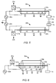
- Fig. 11 shows a simplified block diagram illustrating the principal elements of a modular lithography apparatus 500.
- the lithography apparatus 500 is preferably designed in a modular fashion to permit ease of maintenance.
- Major subsystems are preferably constructed in self-contained and removable modules, so that they can be removed from the lithography apparatus with as little disturbance to other subsystems as possible. This is particularly advantageous for a lithography machine enclosed in a vacuum chamber, where access to the machine is limited. Thus, a faulty subsystem can be removed and replaced quickly, without unnecessarily disconnecting or disturbing other systems.
- these modular subsystems include an illumination optics module 501 including a charged particle beam source 301 and beam collimating system 302, an aperture array and condenser lens module 502 including aperture array 303 and condenser lens array 304, a beam switching module 503 including a multi-aperture array 305 and beamlet blanker array 306, and projection optics module 504 including beam stop array 308, beam deflector array 309, and projection lens arrays 310.
- the modules are designed to slide in and out from an alignment frame.
- the alignment frame comprises an alignment inner subframe 505 suspended via vibration damping mounts 530 from an alignment outer subframe 506.
- a frame 508 supports the alignment subframe 506 via vibration damping mounts 507.
- the target or wafer 330 rests on substrate support structure 509, which is in turn placed on a chuck 510.
- the chuck 510 sits on the stage short stroke 511 and long stroke 512 arranged to move the stage in various horizontal and vertical directions.
- the lithography machine is enclosed in vacuum chamber 335, which may include a mu metal shielding layer or layers 515, and rests on base plate 520 supported by frame members 521.
- Sensor set 401 is arranged to measure distance between the final lens element and the target 330, as shown e.g. in Fig. 10 .
- Sensor set 402 is arranged to measure distance between an optical alignment sensor mounted near the final lens element and the target 330 or chuck 510, to facilitate focusing of the alignment sensor beam for alignment of the target and stage.
- Sensor set 403 is arranged to measure the position of the short stroke stage 511 in horizontal (X, Y-axis) and vertical (Z-axis) positions by measuring distances with respect to the long stroke stage 512.
- Sensor set 404 is arranged for measuring position of the suspended subframe 505 with respect to alignment subframe 506 in horizontal and vertical positions by measurement with respect to the subframe 505.
- Sensor set 405 is arranged for measuring position of the illumination optics module 501 in horizontal and vertical positions by measurement with respect to the subframe 505.
- the capacitive sensors used in any of the applications shown in Figs. 10 and 11 are preferably thin film sensors, and may also be arranged in pairs for differential operation.
- the sensors may be of the type shown in Fig. 8 , preferably connected to the cable 30 using the arrangement shown in Fig. 8 .
- the sensors may also be constructed with multiple sensing electrodes on a signal substrate, such as the sensor pair shown in Fig. 9A, 9B .
- Use of a thin film construction enables the sensors to be constructed at low cost, and enables the sensors to be placed in narrow spaces and on parts of the lithography machine not suitable for conventional sensors with larger dimensions.
- These sets of sensors may be arranged in sets of six sensors to from three differential sensor pairs, for measurement in three axes, i.e. horizontal X, Y-axes and vertical Z-axis directions. This may be accomplished by mounting the differential sensor pairs oriented for measuring distance to each direction to a suitable opposing surface. Measurement signals from the sensors may be sued to adjust the position of moveable parts of the lithography machine, e.g. using a piezomotor to make small movements to obtain proper alignment of the part within the system.
- Each set of sensors is connected via a cable 30 to a corresponding current measurement circuit located in a cabinet outside the vacuum chamber and remote from the lithography machine.
- Fig. 19 shows an embodiment of a cabinet 600 housing circuit boards 601.
- Each circuit board 601 provides the current measurement circuits for a capacitive sensor 40, a pair of circuit boards 602 providing the current measurement circuits for a differential sensor pair.
- a signal generator 605 provides the AC voltage signal for energizing the capacitive sensors, e.g. a triangular voltage waveform from voltage source 20 as described herein.
- Each circuit board is connected via connector 612 and cable 30 to a thin film capacitive sensor 40.
- Current measurement output signals are output via another connector to analog-to-digital converter 613 for conversion to digital signals for use in controlling the lithography machine.
- Power supply 610 provides power to the circuit boards via power supply connector 611.
- the current measurement circuits 21, 21a, 21b may be implemented, for example, as a current-to-voltage converter or a current-to-current converter. There are several factors which contribute to errors in such measurement circuits. These include stray impedance in the input circuitry of the measuring circuit, a limited common mode rejection ratio (CMRR) of the input circuitry, and inaccuracy on the transfer function of the measurement circuit independent of common mode.
- CMRR common mode rejection ratio
- Fig. 12 is a functional schematic diagram of a current measuring circuit 70.
- the input current I CS at input terminal 72 from an AC or DC current source CS is to be measured by the circuit.
- a portion of the current I CS is diverted in the input circuitry of the measuring circuit, this portion represented by current I CM .
- Voltage disturbances on the input terminal 72 relative to the power supply voltages of the circuit cause variation in current I CM flowing through the internal impedance Z CM .
- the current I meas actually measured by the circuit is slightly less than the input current I CS desired to be measured, leading to a small error in the measurement.
- the current I CM results from stray impedances in the input circuitry and common mode disturbances in the input signal. A steady-state error can be connected, but it is very difficult to compensate for the current flow I CM because the value of the stray impedance is variable, depending on factors such as temperature, and common mode disturbances on the input also vary with time.
- the voltage supply terminals 75 and 76 of the current measuring circuit are connected to a power supply comprising voltage sources 77a, 77b.
- a voltage source VD is provided to feed voltage disturbances at the input terminal into the power supply, to that voltage differences between the input signal and the measuring circuit supply voltages remain constant.
- the voltage source VD is connected to the measuring circuit power supply, so that the power supply voltages are also driven by any voltages present at the input terminal of the measuring circuit.
- the voltage source VD may be provided by suitable feedback or feed forward in the circuit.
- Fig. 13 is a functional schematic diagram showing the current measuring circuit of Fig. 12 where the voltage source VD is used to energize a load 71. Driving the load 71 with the voltage source VD results in current I CS which is the current measured at the input terminal 72 of the circuit.
- the disturbance voltage VD which is coupled to the power supply of the current measuring circuit is the voltage which drives the load 71 to produce the current I CS to be measured. Feeding the disturbance voltage into the power supply of the current measuring circuit results in removing the varying voltage differences within the current measuring circuit caused by the disturbance voltage. This removes a source of error in the current measurement.
- the disturbance voltage VD is also subtracted from the output of the current measuring circuit 70 by a difference circuit 79.
- the output signal at the output terminal 74 of the current measuring circuit 70 will have the disturbance voltage VD superimposed on the signal resulting from measuring the input current I CS .
- Subtracting the disturbance voltage VD thus may be used to isolate the portion of the output signal representing the input current measurement.
- the embodiment in Fig. 13 shows two power supply terminals powered by two voltage sources 77a, 77b, typically supplying a positive and a negative DC voltage to positive and negative power supply terminals.
- a single power supply terminal and/or a single power supply voltage source may be used instead.
- the disturbance voltage is fed via capacitors 78a, 78b to the power supply terminals so that the AC component of the disturbance voltage is fed to the power supply terminals while the DC component of the power supply voltages are isolated from the input terminal 72 and the voltage source VD.
- Inductors may also be used to isolate the AC component of the disturbance voltage from the power supply voltages, such as inductors 95, 96 shown in the embodiment in Fig. 15 .
- Fig. 14 is a diagram showing an embodiment of the current measuring circuit implemented with an operational amplifier 80 (referred to as an opamp).
- a current source CS is connected to a negative terminal 82 of the opamp 80, and a positive input terminal 83 of the opamp is connected to common.
- the opamp 80 has two power terminals 85 and 86, through which the operational amplifier 80 can be energized by the two voltage sources 91 and 92.
- the current source CS produces a current Ics to be measured.
- An impedance 87 connected between the input terminal 82 and the output terminal 84 provides negative feedback, and the opamp 80 operates to maintain the voltage difference between the two input terminals 82 and 83 at nearly zero.
- the opamp 80 has a very high input impedance so that very little of the current Ics flows into the opamp, but instead flows through impedance 87.
- the opamp 80 cannot completely eliminate the influences of common mode voltages on the inputs.
- an AC voltage supply VG is used to drive the input terminal 83. Because the opamp 80 is configured to maintain the two input terminals 82 and 83 at almost the same voltage, the voltage VD effectively represents a common mode disturbance on the input terminals.
- the output of the voltage source VD, connected to the input terminal 83, is also connected to the opamp power supply circuit to feedforward the common mode disturbance voltages into the power supply voltages of the opamp 80.
- the output of the voltage source VD is connected via capacitors 93, 94 to couple the voltage at input terminal 83 to the voltage supply to power supply terminals 85, 86.
- DC voltage sources 91, 92 supply a DC voltage to power supply terminals 85, 86 while AC voltages present at input terminal 83 are also supplied to the power supply terminals 85, 86.
- Inductors 95, 96 may also be included in the power supply as shown in the embodiment in Fig. 15 to provide some isolation between the AC components of the feedforward input terminal voltage and the DC voltage sources 77, 78.
- Fig. 15 shows an example of the embodiment of Fig. 14 used for measuring current in a capacitive sensor system, such as shown in any of Figs. 3-6 .
- the current to be measured is transferred to the current measuring circuit 21 via cable 30, as the current measuring circuit 21 is typically located remotely from the capacitive sensor.
- the capacitive sensor may be a thin film capacitive sensor such as shown in Fig. 8 and 9 .
- the cable 30 comprises a sensor wire 31 and a shield conductor 32 and has a remote end and a local end.
- the sensor wire 31 is electrically connected to the capacitive sensor electrode 41 at the local end of the cable 30, and the shield conductor 32 is electrically connected to the capacitive sensor guard electrode 42 at the local end of the cable 30.
- the voltage source 20 energizes the shield conductor 32 at the remote end of the cable 30 to energize the guard electrode 42.
- the voltage source 20 also energizes the sensor wire 31 via the opamp 80 to energize the sensing electrode 41 of the capacitive sensor. Because the opamp maintains the voltages at its input terminals 82, 83 at essentially the same voltage, the sensor wire 31 and shield conductor 32 are also energized at essentially the same voltage, virtually eliminating capacitive leakage current between them.
- the output terminal of the voltage source 20 is connected to input terminal 83, the shield conductor 32, and is also connected to the power supply for the opamp 80 as described earlier, and is connected to a difference circuit 88 to subtract the signal from the voltage source 20 from the output signal of the opamp 80.
- the voltage source preferably provides a triangular voltage signal to drive the capacitive sensor, as described earlier. This results (ideally) in a square-wave current signal shown in Fig. 16A , as described earlier.
- the triangular voltage output by the voltage source 20 is present on input terminals 83 and 82 of the opamp 80, as shown in Fig. 16B .
- the output voltage Vout at the output terminal 84 of the opamp 80 will include the triangular voltage present at the input terminals with a square-wave superimposed due to the square-wave current flowing through the feedback impedance 87, as shown in Fig. 16C .
- the triangular voltage waveform from the voltage source 20 is subtracted by the difference circuit 88 from the signal at the output terminal 84.
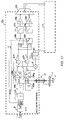
- Fig. 17 shows an embodiment of a voltage source and current measurement circuit for a differential pair sensing system such as described herein. This circuit could also be used for single sensors not operating as a differential pair.
- the circuitry is divided into an analog signal processing portion 50, and a digital signal processing portion 63 which may be implemented e.g. in a field programmable gate array.
- a frequency reference F SYNC is generated (e.g. at 2 MHz) and divided in divider circuit 51 to generate multiple separate square-wave signals at a lower frequency with certain predetermined phase offsets.
- four separate 500 kHz square-wave signals are generated with 90 degree phase offsets.
- Fig. 18A shows an example of square wave frequency reference signal
- Figs. 18B-18E show example waveforms of lower frequency signals with 0, 90, 180 and 270 degree phase shifts.
- Integrator circuit 52 generates a triangular voltage waveform from one of the square-wave signals, and from this the amplifier circuits 53a and 53b generate two triangular voltage waveforms 180 degrees out-of-phase.
- these two out-of-phase triangular voltage waveforms may correspond to the outputs of voltage sources (e.g. 20, 20a, 20b, VD) shown in any of Figs. 3-6 , 13 , 14 or 16 for driving a single capacitive sensor or load or two sensors/loads operated in a differential pair.
- Figs. 18F and 18G show an example of triangular waveform outputs from amplifier circuits 53a and 53b.
- the triangular voltage signals may be connected to energize the shield conductors 32, 32a, 32b, and also the sensor wires 31, 31a, 31b via current-to-voltage converters 54a and 54b, for energizing the capacitive sensors or loads 40, 40a, 40b, 71 as shown in Figs. 3-6 , 13 , 14 or 16 .
- the current-to-voltage converters 54a and 54b generate voltage signals at their outputs representing a measurement of the current signals at their inputs (i.e. the output signals 22, 22a, 22b, 74, 84 of Figs. 3-6 , 13 , 14 or 16 ).
- the triangular voltage waveforms from the amplifier circuits 53a, 53b are subtracted from the measured current signals at the outputs of the current-to-voltage converters 54a, 54b by difference circuits 55a, 55b to remove the triangular voltage signal from the current-to-voltage converter output signals, to isolate the measured input current signal.
- Figs. 18H and 18I show examples of the resulting measured current signal waveforms at the output of the difference circuits 55a, 55b.
- Selectors 56a, 56b use one or more of the phase shifted reference signals generated by divider circuit 51, e.g. 180 and 270 degree shifted reference signals shown in Figs. 18D and 18E , to sample a portion of each cycle of the measured current signals shown in Figs. 18H and 18I .
- the second half of each cycle of the measured current signals is sampled to obtain the amplitude for the portion of the cycle when it is generally steady-state at the maximum amplitude value.
- the sampling may be performed to switch between the two measured current signals, to accumulate the positive amplitudes in one signal ( Fig. 18J ) and the negative amplitudes in the other signal ( Fig. 18K ).
- Low pass filters 57a, 57b filter the sampled measured current signals to implement an equivalent of a capacitor charging circuit with slope determined by the amplitude of the sampled portion of the measured current signal waveform.
- Example waveforms at the output of amplifiers 58a, 58b are shown in Figs. 18J and 18K .
- the waveforms rise (or fall) during each sampled period, the end values determined by the amplitude of the measured current signals.
- the outputs from the amplifiers 58a, 58b are subtracted from each other and the resulting signal is converted to a digital signal by analog-to-digital converter 59.
- the resulting digital signal is output to the digital signal processing circuitry 63 for further processing such as calibration adjustment and scaling to result in a useable measurement indicative of the sensor capacitance.
- Adder 61 and window comparator 62 generate an error signal for use in the digital signal processing circuitry 63 for situations such as a cable short or open fault.
Landscapes
- Physics & Mathematics (AREA)
- General Physics & Mathematics (AREA)
- Engineering & Computer Science (AREA)
- Power Engineering (AREA)
- Measurement Of Length, Angles, Or The Like Using Electric Or Magnetic Means (AREA)
- Measurement Of Current Or Voltage (AREA)
- Transmission And Conversion Of Sensor Element Output (AREA)
- Electron Beam Exposure (AREA)
- Exposure And Positioning Against Photoresist Photosensitive Materials (AREA)
- Measuring Instrument Details And Bridges, And Automatic Balancing Devices (AREA)
- Exposure Of Semiconductors, Excluding Electron Or Ion Beam Exposure (AREA)
Applications Claiming Priority (2)
| Application Number | Priority Date | Filing Date | Title |
|---|---|---|---|
| US201161503555P | 2011-06-30 | 2011-06-30 | |
| PCT/EP2012/062851 WO2013001098A2 (en) | 2011-06-30 | 2012-07-02 | Active shield for capacitive measurement system |
Publications (2)
| Publication Number | Publication Date |
|---|---|
| EP2726822A2 EP2726822A2 (en) | 2014-05-07 |
| EP2726822B1 true EP2726822B1 (en) | 2016-11-09 |
Family
ID=46420210
Family Applications (2)
| Application Number | Title | Priority Date | Filing Date |
|---|---|---|---|
| EP12730982.1A Active EP2726822B1 (en) | 2011-06-30 | 2012-07-02 | Active shield for capacitive measurement system |
| EP12732640.3A Active EP2726823B1 (en) | 2011-06-30 | 2012-07-02 | System for measuring an input electrical current |
Family Applications After (1)
| Application Number | Title | Priority Date | Filing Date |
|---|---|---|---|
| EP12732640.3A Active EP2726823B1 (en) | 2011-06-30 | 2012-07-02 | System for measuring an input electrical current |
Country Status (8)
| Country | Link |
|---|---|
| US (3) | US9644995B2 (ru) |
| EP (2) | EP2726822B1 (ru) |
| JP (2) | JP2014527616A (ru) |
| KR (3) | KR101875415B1 (ru) |
| CN (2) | CN103635780A (ru) |
| RU (1) | RU2610221C2 (ru) |
| TW (2) | TWI564543B (ru) |
| WO (2) | WO2013001100A1 (ru) |
Families Citing this family (26)
| Publication number | Priority date | Publication date | Assignee | Title |
|---|---|---|---|---|
| EP2735868B1 (en) * | 2012-11-26 | 2015-11-25 | University College Cork | Nanowire electrode sensor |
| US9423418B2 (en) * | 2013-02-25 | 2016-08-23 | Google Technology Holdings LLC | Capacitive sensor |
| EP2781234A1 (en) * | 2013-03-20 | 2014-09-24 | Fresenius Medical Care Deutschland GmbH | Tube for extra-corporeal circuit with double connector |
| US20140292354A1 (en) * | 2013-03-27 | 2014-10-02 | Texas Instruments Incorporated | Capacitive sensor |
| US9739816B2 (en) | 2013-11-27 | 2017-08-22 | Analog Devices, Inc. | Capacitive sensor with differential shield |
| CN103884901B (zh) * | 2014-04-04 | 2016-06-08 | 哈尔滨理工大学 | 一种基于fp电压传感器的高电压测量系统及测量方法 |
| US9983228B2 (en) * | 2014-09-24 | 2018-05-29 | Keithley Instruments, Llc | Triaxial DC-AC connection system |
| WO2017207037A1 (en) * | 2016-05-31 | 2017-12-07 | Telecom Italia S.P.A. | Meter apparatus for measuring parameters of electrical quantity |
| US10139435B2 (en) * | 2016-11-11 | 2018-11-27 | Fluke Corporation | Non-contact voltage measurement system using reference signal |
| CN108195490B (zh) * | 2018-01-31 | 2019-10-11 | 北京他山科技有限公司 | 具有分时、分区域屏蔽功能的传感器、电子皮肤和机器人 |
| CN108808685B (zh) * | 2018-03-26 | 2020-12-11 | 北京航天发射技术研究所 | 一种电源电压数字式补偿系统及方法 |
| US11493394B2 (en) * | 2018-03-30 | 2022-11-08 | Panasonic Intellectual Property Management Co., Ltd. | Capacitance detection device |
| JP7122686B2 (ja) * | 2018-03-30 | 2022-08-22 | パナソニックIpマネジメント株式会社 | 静電容量検出装置 |
| DE102018003268A1 (de) * | 2018-04-19 | 2019-11-07 | Technische Universität Chemnitz | Einrichtung zur Bestimmung der elektrischen Kapazität |
| US10551416B2 (en) * | 2018-05-09 | 2020-02-04 | Fluke Corporation | Multi-sensor configuration for non-contact voltage measurement devices |
| US11141767B2 (en) * | 2018-07-30 | 2021-10-12 | Raytheon Technologies Corporation | Forging assembly having capacitance sensors |
| US10837803B2 (en) * | 2019-04-12 | 2020-11-17 | Kla Corporation | Inspection system with grounded capacitive sample proximity sensor |
| JP7281124B2 (ja) * | 2019-07-29 | 2023-05-25 | 国立研究開発法人量子科学技術研究開発機構 | 角度センサ、マウント装置、及び測定方法 |
| US11874423B2 (en) | 2019-10-25 | 2024-01-16 | Witricity Corporation | Circuit for object detection and vehicle position determination |
| CN114121374B (zh) * | 2020-08-27 | 2023-01-13 | 华为技术有限公司 | 一种同轴电缆和终端 |
| US11784482B2 (en) * | 2020-10-20 | 2023-10-10 | Apple Inc. | Electrical connection monitoring using cable shielding |
| EP4285462A1 (en) * | 2021-01-26 | 2023-12-06 | WiTricity Corporation | Wire-wound structures for electromagnetic sensing of objects |
| US11750041B2 (en) * | 2021-01-26 | 2023-09-05 | Witricity Corporation | Wire-wound structures for electromagnetic sensing of objects |
| EP4050353A1 (en) | 2021-02-25 | 2022-08-31 | Infineon Technologies AG | An apparatus and a method for measuring a device current of a device under test |
| CN114812618B (zh) * | 2021-12-24 | 2023-03-07 | 中国科学院长春光学精密机械与物理研究所 | 频点噪声抑制系统 |
| CN116338142B (zh) * | 2023-02-28 | 2024-02-27 | 浙江大学 | 一种超重力实验中水合物储层表面变形测量装置和方法 |
Family Cites Families (41)
| Publication number | Priority date | Publication date | Assignee | Title |
|---|---|---|---|---|
| US3101024A (en) | 1959-10-05 | 1963-08-20 | Lanston Ind Inc | All-purpose photographic mechanical reproduction camera |
| US3713022A (en) | 1971-12-17 | 1973-01-23 | Systomation Inc | Capacitance measurement by phase-controlled sampling |
| JPS5728266A (en) | 1980-07-28 | 1982-02-15 | Hitachi Ltd | Digital ammeter |
| SU1160321A1 (ru) | 1982-03-05 | 1985-06-07 | Гомельский Государственный Университет | Устройство дл измерени амплитудных значений переменных электрических сигналов |
| US4538069A (en) * | 1983-10-28 | 1985-08-27 | Control Data Corporation | Capacitance height gage applied in reticle position detection system for electron beam lithography apparatus |
| US5489888A (en) | 1990-11-07 | 1996-02-06 | Precitec Gmbh | Sensor system for contactless distance measuring |
| US5539323A (en) * | 1993-05-07 | 1996-07-23 | Brooks Automation, Inc. | Sensor for articles such as wafers on end effector |
| CH689190A5 (fr) | 1993-10-19 | 1998-11-30 | Hans Ulrich Meyer | Instrument de mesure de longueurs ou d'angles. |
| DE9421121U1 (de) * | 1994-11-10 | 1995-04-27 | Siedle Horst Kg | Vorrichtung zur Bestimmung einer jeweiligen örtlichen Position eines Körpers durch kapazitive Abtastung |
| US5730165A (en) | 1995-12-26 | 1998-03-24 | Philipp; Harald | Time domain capacitive field detector |
| AU1608497A (en) | 1996-02-02 | 1997-08-22 | Bicc Public Limited Company | Capacitance transducer apparatus and cables |
| US6014030A (en) * | 1996-05-03 | 2000-01-11 | National Semiconductor Corp. | Current-level monitor with hierarchical precision |
| JP3158063B2 (ja) * | 1997-01-21 | 2001-04-23 | 北斗電子工業株式会社 | 非接触電圧計測方法及び装置 |
| WO1999028756A1 (fr) | 1997-12-02 | 1999-06-10 | Advantest Corporation | Procede permettant de mesurer une intensite en appliquant une tension, et dispositif a cet effet |
| US5963023A (en) * | 1998-03-21 | 1999-10-05 | Advanced Micro Devices, Inc. | Power surge management for high performance integrated circuit |
| DE19836054A1 (de) | 1998-08-10 | 2000-02-17 | Bosch Gmbh Robert | Meßschaltung |
| FR2790095B1 (fr) | 1999-02-18 | 2001-04-06 | Siemens Automotive Sa | Dispositif de mesure de courant et procede correspondant |
| DE19916915B4 (de) * | 1999-04-14 | 2005-08-11 | Infineon Technologies Ag | Schaltnetzteil und Verfahren zur Ermittlung der Versorgungsspannung in einem Schaltnetzteil |
| ATE399327T1 (de) | 2001-09-06 | 2008-07-15 | Tokyo Electron Ltd | Vorrichtung und verfahren zur messung der sensorkapazität |
| US7005864B2 (en) * | 2002-10-21 | 2006-02-28 | Synchrony, Inc. | Capacitive position sensing system with resonant amplification |
| TWI304158B (en) * | 2003-01-15 | 2008-12-11 | Asml Netherlands Bv | Detection assembly and lithographic projection apparatus provided with such a detection assembly |
| JP4067053B2 (ja) * | 2003-03-13 | 2008-03-26 | キヤノン株式会社 | 静電容量センサ式計測装置 |
| DE60308161T2 (de) * | 2003-06-27 | 2007-08-09 | Asml Netherlands B.V. | Lithographischer Apparat und Verfahren zur Herstellung eines Artikels |
| US7141988B2 (en) * | 2003-07-01 | 2006-11-28 | Tiax Llc | Capacitive position sensor and sensing methodology |
| CA2542325A1 (en) * | 2003-10-10 | 2005-04-21 | That Corporation | Low-power integrated-circuit signal processor with wide dynamic range |
| JP2005156492A (ja) * | 2003-11-28 | 2005-06-16 | Agilent Technol Inc | 可動機構、測定装置、静電容量式距離測定装置、および、位置決め装置 |
| US6989679B2 (en) | 2004-06-03 | 2006-01-24 | General Electric Company | Non-contact capacitive sensor and cable with dual layer active shield |
| JP4613523B2 (ja) | 2004-06-16 | 2011-01-19 | ダイキン工業株式会社 | 電流測定装置 |
| US7746048B2 (en) * | 2005-11-11 | 2010-06-29 | L&L Engineering, Llc | Non-linear PWM controller for DC-to-DC converters |
| GB2436619B (en) | 2005-12-19 | 2010-10-06 | Toumaz Technology Ltd | Sensor circuits |
| US8063886B2 (en) | 2006-07-18 | 2011-11-22 | Iee International Electronics & Engineering S.A. | Data input device |
| CN101490642A (zh) | 2006-07-18 | 2009-07-22 | Iee国际电子工程股份公司 | 输入设备 |
| US7764067B2 (en) * | 2007-12-27 | 2010-07-27 | Caterpillar Inc | High voltage cable testing method |
| US20090295366A1 (en) * | 2008-03-20 | 2009-12-03 | Cehelnik Thomas G | E-field sensor arrays for interactive gaming, computer interfaces, machine vision, medical imaging, and geological exploration |
| US8212546B2 (en) * | 2008-03-20 | 2012-07-03 | Entropic Communications, Inc. | Wideband CMOS RMS power detection scheme |
| NL1036623A1 (nl) | 2008-03-26 | 2009-09-29 | Asml Netherlands Bv | Lithographic apparatus and device manufacturing method. |
| JP2011053201A (ja) * | 2009-04-30 | 2011-03-17 | Hioki Ee Corp | 電圧検出装置および線間電圧検出装置 |
| CN101881791B (zh) | 2009-04-30 | 2015-08-05 | 日置电机株式会社 | 电压检测装置 |
| JP5340817B2 (ja) * | 2009-06-11 | 2013-11-13 | 日置電機株式会社 | 電圧検出装置 |
| CN101762736A (zh) | 2009-11-09 | 2010-06-30 | 天津南大强芯半导体芯片设计有限公司 | 一种镜像电流检测电路 |
| US8513959B2 (en) | 2009-12-31 | 2013-08-20 | Mapper Lithography Ip B.V. | Integrated sensor system |
-
2012
- 2012-07-02 US US13/539,585 patent/US9644995B2/en not_active Ceased
- 2012-07-02 CN CN201280032498.9A patent/CN103635780A/zh active Pending
- 2012-07-02 EP EP12730982.1A patent/EP2726822B1/en active Active
- 2012-07-02 CN CN201280032762.9A patent/CN103649688B/zh active Active
- 2012-07-02 KR KR1020147002592A patent/KR101875415B1/ko active IP Right Grant
- 2012-07-02 KR KR1020187018729A patent/KR102152297B1/ko active IP Right Grant
- 2012-07-02 WO PCT/EP2012/062854 patent/WO2013001100A1/en active Application Filing
- 2012-07-02 JP JP2014517764A patent/JP2014527616A/ja not_active Withdrawn
- 2012-07-02 EP EP12732640.3A patent/EP2726823B1/en active Active
- 2012-07-02 RU RU2014102968A patent/RU2610221C2/ru active
- 2012-07-02 US US13/539,561 patent/US9400195B2/en active Active
- 2012-07-02 WO PCT/EP2012/062851 patent/WO2013001098A2/en active Application Filing
- 2012-07-02 KR KR1020207025064A patent/KR102236200B1/ko active IP Right Grant
- 2012-07-02 TW TW101123857A patent/TWI564543B/zh active
- 2012-07-02 TW TW101123858A patent/TWI568990B/zh active
-
2017
- 2017-04-19 JP JP2017082981A patent/JP6463793B2/ja active Active
-
2019
- 2019-05-09 US US16/408,309 patent/USRE48901E1/en active Active
Also Published As
| Publication number | Publication date |
|---|---|
| CN103635780A (zh) | 2014-03-12 |
| KR102236200B1 (ko) | 2021-04-06 |
| JP2014527616A (ja) | 2014-10-16 |
| JP2017201306A (ja) | 2017-11-09 |
| TW201319523A (zh) | 2013-05-16 |
| KR20200105964A (ko) | 2020-09-09 |
| RU2610221C2 (ru) | 2017-02-08 |
| WO2013001098A2 (en) | 2013-01-03 |
| KR20180081155A (ko) | 2018-07-13 |
| WO2013001098A3 (en) | 2013-03-07 |
| TW201307804A (zh) | 2013-02-16 |
| US9400195B2 (en) | 2016-07-26 |
| WO2013001100A4 (en) | 2013-02-14 |
| CN103649688B (zh) | 2017-02-22 |
| EP2726822A2 (en) | 2014-05-07 |
| TWI564543B (zh) | 2017-01-01 |
| US20130003034A1 (en) | 2013-01-03 |
| RU2014102968A (ru) | 2015-08-10 |
| US9644995B2 (en) | 2017-05-09 |
| EP2726823A1 (en) | 2014-05-07 |
| USRE48901E1 (en) | 2022-01-25 |
| KR20140058525A (ko) | 2014-05-14 |
| KR102152297B1 (ko) | 2020-09-07 |
| EP2726823B1 (en) | 2017-06-21 |
| WO2013001098A4 (en) | 2013-05-02 |
| TWI568990B (zh) | 2017-02-01 |
| CN103649688A (zh) | 2014-03-19 |
| KR101875415B1 (ko) | 2018-07-06 |
| JP6463793B2 (ja) | 2019-02-06 |
| US20130009626A1 (en) | 2013-01-10 |
| WO2013001100A1 (en) | 2013-01-03 |
Similar Documents
| Publication | Publication Date | Title |
|---|---|---|
| USRE48901E1 (en) | Current measurement system | |
| KR101436947B1 (ko) | 통합 센서 시스템 | |
| NL2004055C2 (en) | Method for measuring target surface topology and lithography system. | |
| NL2004052C2 (en) | Capacitive sensing system. | |
| NL2004051C2 (en) | Capacitive sensor. | |
| NL2004054C2 (en) | Lithography system with capacitive sensing system. |
Legal Events
| Date | Code | Title | Description |
|---|---|---|---|
| PUAI | Public reference made under article 153(3) epc to a published international application that has entered the european phase |
Free format text: ORIGINAL CODE: 0009012 |
|
| 17P | Request for examination filed |
Effective date: 20140130 |
|
| AK | Designated contracting states |
Kind code of ref document: A2 Designated state(s): AL AT BE BG CH CY CZ DE DK EE ES FI FR GB GR HR HU IE IS IT LI LT LU LV MC MK MT NL NO PL PT RO RS SE SI SK SM TR |
|
| DAX | Request for extension of the european patent (deleted) | ||
| 17Q | First examination report despatched |
Effective date: 20151111 |
|
| GRAP | Despatch of communication of intention to grant a patent |
Free format text: ORIGINAL CODE: EPIDOSNIGR1 |
|
| INTG | Intention to grant announced |
Effective date: 20160602 |
|
| GRAS | Grant fee paid |
Free format text: ORIGINAL CODE: EPIDOSNIGR3 |
|
| GRAA | (expected) grant |
Free format text: ORIGINAL CODE: 0009210 |
|
| AK | Designated contracting states |
Kind code of ref document: B1 Designated state(s): AL AT BE BG CH CY CZ DE DK EE ES FI FR GB GR HR HU IE IS IT LI LT LU LV MC MK MT NL NO PL PT RO RS SE SI SK SM TR |
|
| REG | Reference to a national code |
Ref country code: GB Ref legal event code: FG4D |
|
| REG | Reference to a national code |
Ref country code: AT Ref legal event code: REF Ref document number: 844358 Country of ref document: AT Kind code of ref document: T Effective date: 20161115 Ref country code: CH Ref legal event code: EP |
|
| REG | Reference to a national code |
Ref country code: IE Ref legal event code: FG4D |
|
| REG | Reference to a national code |
Ref country code: DE Ref legal event code: R096 Ref document number: 602012025146 Country of ref document: DE |
|
| REG | Reference to a national code |
Ref country code: NL Ref legal event code: FP |
|
| REG | Reference to a national code |
Ref country code: CH Ref legal event code: NV Representative=s name: FIAMMENGHI-FIAMMENGHI, CH |
|
| PG25 | Lapsed in a contracting state [announced via postgrant information from national office to epo] |
Ref country code: LV Free format text: LAPSE BECAUSE OF FAILURE TO SUBMIT A TRANSLATION OF THE DESCRIPTION OR TO PAY THE FEE WITHIN THE PRESCRIBED TIME-LIMIT Effective date: 20161109 |
|
| REG | Reference to a national code |
Ref country code: SE Ref legal event code: TRGR |
|
| REG | Reference to a national code |
Ref country code: LT Ref legal event code: MG4D |
|
| PG25 | Lapsed in a contracting state [announced via postgrant information from national office to epo] |
Ref country code: GR Free format text: LAPSE BECAUSE OF FAILURE TO SUBMIT A TRANSLATION OF THE DESCRIPTION OR TO PAY THE FEE WITHIN THE PRESCRIBED TIME-LIMIT Effective date: 20170210 Ref country code: NO Free format text: LAPSE BECAUSE OF FAILURE TO SUBMIT A TRANSLATION OF THE DESCRIPTION OR TO PAY THE FEE WITHIN THE PRESCRIBED TIME-LIMIT Effective date: 20170209 Ref country code: LT Free format text: LAPSE BECAUSE OF FAILURE TO SUBMIT A TRANSLATION OF THE DESCRIPTION OR TO PAY THE FEE WITHIN THE PRESCRIBED TIME-LIMIT Effective date: 20161109 |
|
| REG | Reference to a national code |
Ref country code: FR Ref legal event code: PLFP Year of fee payment: 6 |
|
| PG25 | Lapsed in a contracting state [announced via postgrant information from national office to epo] |
Ref country code: PT Free format text: LAPSE BECAUSE OF FAILURE TO SUBMIT A TRANSLATION OF THE DESCRIPTION OR TO PAY THE FEE WITHIN THE PRESCRIBED TIME-LIMIT Effective date: 20170309 Ref country code: RS Free format text: LAPSE BECAUSE OF FAILURE TO SUBMIT A TRANSLATION OF THE DESCRIPTION OR TO PAY THE FEE WITHIN THE PRESCRIBED TIME-LIMIT Effective date: 20161109 Ref country code: IS Free format text: LAPSE BECAUSE OF FAILURE TO SUBMIT A TRANSLATION OF THE DESCRIPTION OR TO PAY THE FEE WITHIN THE PRESCRIBED TIME-LIMIT Effective date: 20170309 Ref country code: ES Free format text: LAPSE BECAUSE OF FAILURE TO SUBMIT A TRANSLATION OF THE DESCRIPTION OR TO PAY THE FEE WITHIN THE PRESCRIBED TIME-LIMIT Effective date: 20161109 Ref country code: FI Free format text: LAPSE BECAUSE OF FAILURE TO SUBMIT A TRANSLATION OF THE DESCRIPTION OR TO PAY THE FEE WITHIN THE PRESCRIBED TIME-LIMIT Effective date: 20161109 Ref country code: PL Free format text: LAPSE BECAUSE OF FAILURE TO SUBMIT A TRANSLATION OF THE DESCRIPTION OR TO PAY THE FEE WITHIN THE PRESCRIBED TIME-LIMIT Effective date: 20161109 Ref country code: HR Free format text: LAPSE BECAUSE OF FAILURE TO SUBMIT A TRANSLATION OF THE DESCRIPTION OR TO PAY THE FEE WITHIN THE PRESCRIBED TIME-LIMIT Effective date: 20161109 |
|
| PG25 | Lapsed in a contracting state [announced via postgrant information from national office to epo] |
Ref country code: SK Free format text: LAPSE BECAUSE OF FAILURE TO SUBMIT A TRANSLATION OF THE DESCRIPTION OR TO PAY THE FEE WITHIN THE PRESCRIBED TIME-LIMIT Effective date: 20161109 Ref country code: CZ Free format text: LAPSE BECAUSE OF FAILURE TO SUBMIT A TRANSLATION OF THE DESCRIPTION OR TO PAY THE FEE WITHIN THE PRESCRIBED TIME-LIMIT Effective date: 20161109 Ref country code: EE Free format text: LAPSE BECAUSE OF FAILURE TO SUBMIT A TRANSLATION OF THE DESCRIPTION OR TO PAY THE FEE WITHIN THE PRESCRIBED TIME-LIMIT Effective date: 20161109 Ref country code: RO Free format text: LAPSE BECAUSE OF FAILURE TO SUBMIT A TRANSLATION OF THE DESCRIPTION OR TO PAY THE FEE WITHIN THE PRESCRIBED TIME-LIMIT Effective date: 20161109 Ref country code: DK Free format text: LAPSE BECAUSE OF FAILURE TO SUBMIT A TRANSLATION OF THE DESCRIPTION OR TO PAY THE FEE WITHIN THE PRESCRIBED TIME-LIMIT Effective date: 20161109 |
|
| REG | Reference to a national code |
Ref country code: DE Ref legal event code: R097 Ref document number: 602012025146 Country of ref document: DE |
|
| PG25 | Lapsed in a contracting state [announced via postgrant information from national office to epo] |
Ref country code: BE Free format text: LAPSE BECAUSE OF FAILURE TO SUBMIT A TRANSLATION OF THE DESCRIPTION OR TO PAY THE FEE WITHIN THE PRESCRIBED TIME-LIMIT Effective date: 20161109 Ref country code: BG Free format text: LAPSE BECAUSE OF FAILURE TO SUBMIT A TRANSLATION OF THE DESCRIPTION OR TO PAY THE FEE WITHIN THE PRESCRIBED TIME-LIMIT Effective date: 20170209 Ref country code: SM Free format text: LAPSE BECAUSE OF FAILURE TO SUBMIT A TRANSLATION OF THE DESCRIPTION OR TO PAY THE FEE WITHIN THE PRESCRIBED TIME-LIMIT Effective date: 20161109 |
|
| PLBE | No opposition filed within time limit |
Free format text: ORIGINAL CODE: 0009261 |
|
| STAA | Information on the status of an ep patent application or granted ep patent |
Free format text: STATUS: NO OPPOSITION FILED WITHIN TIME LIMIT |
|
| 26N | No opposition filed |
Effective date: 20170810 |
|
| PG25 | Lapsed in a contracting state [announced via postgrant information from national office to epo] |
Ref country code: SI Free format text: LAPSE BECAUSE OF FAILURE TO SUBMIT A TRANSLATION OF THE DESCRIPTION OR TO PAY THE FEE WITHIN THE PRESCRIBED TIME-LIMIT Effective date: 20161109 |
|
| REG | Reference to a national code |
Ref country code: FR Ref legal event code: PLFP Year of fee payment: 7 |
|
| PG25 | Lapsed in a contracting state [announced via postgrant information from national office to epo] |
Ref country code: LU Free format text: LAPSE BECAUSE OF NON-PAYMENT OF DUE FEES Effective date: 20170702 |
|
| PG25 | Lapsed in a contracting state [announced via postgrant information from national office to epo] |
Ref country code: MT Free format text: LAPSE BECAUSE OF NON-PAYMENT OF DUE FEES Effective date: 20170702 |
|
| REG | Reference to a national code |
Ref country code: NL Ref legal event code: PD Owner name: ASML NETHERLANDS B.V.; NL Free format text: DETAILS ASSIGNMENT: CHANGE OF OWNER(S), ASSIGNMENT; FORMER OWNER NAME: MAPPER LITHOGRAPHY IP B.V. Effective date: 20190425 |
|
| REG | Reference to a national code |
Ref country code: AT Ref legal event code: UEP Ref document number: 844358 Country of ref document: AT Kind code of ref document: T Effective date: 20161109 |
|
| PG25 | Lapsed in a contracting state [announced via postgrant information from national office to epo] |
Ref country code: MC Free format text: LAPSE BECAUSE OF FAILURE TO SUBMIT A TRANSLATION OF THE DESCRIPTION OR TO PAY THE FEE WITHIN THE PRESCRIBED TIME-LIMIT Effective date: 20161109 Ref country code: HU Free format text: LAPSE BECAUSE OF FAILURE TO SUBMIT A TRANSLATION OF THE DESCRIPTION OR TO PAY THE FEE WITHIN THE PRESCRIBED TIME-LIMIT; INVALID AB INITIO Effective date: 20120702 |
|
| PG25 | Lapsed in a contracting state [announced via postgrant information from national office to epo] |
Ref country code: CY Free format text: LAPSE BECAUSE OF NON-PAYMENT OF DUE FEES Effective date: 20161109 |
|
| PG25 | Lapsed in a contracting state [announced via postgrant information from national office to epo] |
Ref country code: MK Free format text: LAPSE BECAUSE OF FAILURE TO SUBMIT A TRANSLATION OF THE DESCRIPTION OR TO PAY THE FEE WITHIN THE PRESCRIBED TIME-LIMIT Effective date: 20161109 |
|
| PG25 | Lapsed in a contracting state [announced via postgrant information from national office to epo] |
Ref country code: TR Free format text: LAPSE BECAUSE OF FAILURE TO SUBMIT A TRANSLATION OF THE DESCRIPTION OR TO PAY THE FEE WITHIN THE PRESCRIBED TIME-LIMIT Effective date: 20161109 |
|
| PG25 | Lapsed in a contracting state [announced via postgrant information from national office to epo] |
Ref country code: AL Free format text: LAPSE BECAUSE OF FAILURE TO SUBMIT A TRANSLATION OF THE DESCRIPTION OR TO PAY THE FEE WITHIN THE PRESCRIBED TIME-LIMIT Effective date: 20161109 |
|
| PGFP | Annual fee paid to national office [announced via postgrant information from national office to epo] |
Ref country code: SE Payment date: 20220722 Year of fee payment: 11 Ref country code: IT Payment date: 20220725 Year of fee payment: 11 Ref country code: IE Payment date: 20220719 Year of fee payment: 11 Ref country code: GB Payment date: 20220719 Year of fee payment: 11 |
|
| PGFP | Annual fee paid to national office [announced via postgrant information from national office to epo] |
Ref country code: CH Payment date: 20220726 Year of fee payment: 11 |
|
| P01 | Opt-out of the competence of the unified patent court (upc) registered |
Effective date: 20230403 |
|
| PGFP | Annual fee paid to national office [announced via postgrant information from national office to epo] |
Ref country code: NL Payment date: 20230726 Year of fee payment: 12 |
|
| PGFP | Annual fee paid to national office [announced via postgrant information from national office to epo] |
Ref country code: AT Payment date: 20230718 Year of fee payment: 12 |
|
| PGFP | Annual fee paid to national office [announced via postgrant information from national office to epo] |
Ref country code: FR Payment date: 20230725 Year of fee payment: 12 Ref country code: DE Payment date: 20230726 Year of fee payment: 12 |
|
| REG | Reference to a national code |
Ref country code: CH Ref legal event code: PL |
|
| REG | Reference to a national code |
Ref country code: SE Ref legal event code: EUG |
|
| GBPC | Gb: european patent ceased through non-payment of renewal fee |
Effective date: 20230702 |
|
| PG25 | Lapsed in a contracting state [announced via postgrant information from national office to epo] |
Ref country code: CH Free format text: LAPSE BECAUSE OF NON-PAYMENT OF DUE FEES Effective date: 20230731 Ref country code: GB Free format text: LAPSE BECAUSE OF NON-PAYMENT OF DUE FEES Effective date: 20230702 |