EP2718379B1 - Bottom antireflective coating compositions and processes thereof - Google Patents
Bottom antireflective coating compositions and processes thereof Download PDFInfo
- Publication number
- EP2718379B1 EP2718379B1 EP12731156.1A EP12731156A EP2718379B1 EP 2718379 B1 EP2718379 B1 EP 2718379B1 EP 12731156 A EP12731156 A EP 12731156A EP 2718379 B1 EP2718379 B1 EP 2718379B1
- Authority
- EP
- European Patent Office
- Prior art keywords
- group
- arylene
- photoresist
- hydroxyl
- alkyl
- Prior art date
- Legal status (The legal status is an assumption and is not a legal conclusion. Google has not performed a legal analysis and makes no representation as to the accuracy of the status listed.)
- Active
Links
Images

Classifications
-
- C—CHEMISTRY; METALLURGY
- C09—DYES; PAINTS; POLISHES; NATURAL RESINS; ADHESIVES; COMPOSITIONS NOT OTHERWISE PROVIDED FOR; APPLICATIONS OF MATERIALS NOT OTHERWISE PROVIDED FOR
- C09D—COATING COMPOSITIONS, e.g. PAINTS, VARNISHES OR LACQUERS; FILLING PASTES; CHEMICAL PAINT OR INK REMOVERS; INKS; CORRECTING FLUIDS; WOODSTAINS; PASTES OR SOLIDS FOR COLOURING OR PRINTING; USE OF MATERIALS THEREFOR
- C09D5/00—Coating compositions, e.g. paints, varnishes or lacquers, characterised by their physical nature or the effects produced; Filling pastes
- C09D5/006—Anti-reflective coatings
-
- G—PHYSICS
- G02—OPTICS
- G02B—OPTICAL ELEMENTS, SYSTEMS OR APPARATUS
- G02B1/00—Optical elements characterised by the material of which they are made; Optical coatings for optical elements
- G02B1/10—Optical coatings produced by application to, or surface treatment of, optical elements
- G02B1/11—Anti-reflection coatings
-
- G—PHYSICS
- G03—PHOTOGRAPHY; CINEMATOGRAPHY; ANALOGOUS TECHNIQUES USING WAVES OTHER THAN OPTICAL WAVES; ELECTROGRAPHY; HOLOGRAPHY
- G03F—PHOTOMECHANICAL PRODUCTION OF TEXTURED OR PATTERNED SURFACES, e.g. FOR PRINTING, FOR PROCESSING OF SEMICONDUCTOR DEVICES; MATERIALS THEREFOR; ORIGINALS THEREFOR; APPARATUS SPECIALLY ADAPTED THEREFOR
- G03F7/00—Photomechanical, e.g. photolithographic, production of textured or patterned surfaces, e.g. printing surfaces; Materials therefor, e.g. comprising photoresists; Apparatus specially adapted therefor
- G03F7/004—Photosensitive materials
- G03F7/09—Photosensitive materials characterised by structural details, e.g. supports, auxiliary layers
- G03F7/091—Photosensitive materials characterised by structural details, e.g. supports, auxiliary layers characterised by antireflection means or light filtering or absorbing means, e.g. anti-halation, contrast enhancement
-
- H—ELECTRICITY
- H01—ELECTRIC ELEMENTS
- H01L—SEMICONDUCTOR DEVICES NOT COVERED BY CLASS H10
- H01L21/00—Processes or apparatus adapted for the manufacture or treatment of semiconductor or solid state devices or of parts thereof
- H01L21/02—Manufacture or treatment of semiconductor devices or of parts thereof
- H01L21/027—Making masks on semiconductor bodies for further photolithographic processing not provided for in group H01L21/18 or H01L21/34
Definitions
- the present invention relates to novel antireflective coating compositions and their use in image processing by forming a thin layer of the novel antireflective coating composition between a reflective substrate and a photoresist coating.
- Such compositions are particularly useful in the fabrication of semiconductor devices by photolithographic techniques, especially those requiring exposure with deep ultraviolet radiation.
- Photoresist compositions are used in microlithography processes for making miniaturized electronic components such as in the fabrication of computer chips and integrated circuits.
- a thin coating of a film of a photoresist composition is first applied to a substrate material, such as silicon wafers used for making integrated circuits.
- the coated substrate is then baked to evaporate any solvent in the photoresist composition and to fix the coating onto the substrate.
- the baked and coated surface of the substrate is next subjected to an image-wise exposure to radiation.
- This radiation exposure causes a chemical transformation in the exposed areas of the coated surface.
- Visible light, ultraviolet (UV) light, electron beam and X-ray radiant energy are radiation types commonly used today in microlithographic processes.
- the coated substrate is treated with a developer solution to dissolve and remove either the radiation-exposed or the unexposed areas of the photoresist.
- photoresist compositions there are two types of photoresist compositions, negative-working and positive-working.
- positive-working photoresist compositions When positive-working photoresist compositions are exposed image-wise to radiation, the areas of the photoresist composition exposed to the radiation become soluble in a developer solution while the unexposed areas of the photoresist coating remain relatively insoluble to such a solution.
- treatment of an exposed positive-working photoresist with a developer causes removal of the exposed areas of the photoresist coating and the formation of a positive image in the coating, thereby uncovering a desired portion of the underlying substrate surface on which the photoresist composition was deposited.
- a negative-working photoresist the developer removes the portions that are not exposed.
- the use of absorbing antireflective coatings in photolithography is a simpler approach to diminish the problems that result from back reflection of light from highly reflective substrates.
- the bottom antireflective coating is applied on the substrate and then a layer of photoresist is applied on top of the antireflective coating.
- the photoresist is exposed imagewise and developed.
- the antireflective coating in the exposed area is then typically etched and the photoresist pattern is thus transferred to the substrate.
- Most antireflective coatings known in the prior art are designed to be dry etched.
- the etch rate of the antireflective film needs to be relatively high in comparison to the photoresist so that the antireflective film is etched without excessive loss of the resist film during the etch process.
- photoresist patterns may be damaged or may not be transferred exactly to the substrate if the dry etch rate of the antireflective coating is similar to or less than the etch rate of the photoresist coated on top of the antireflective coating.
- the etching conditions for removing the organic coatings can also damage the substrate.
- US 2008/0161217 A1 discloses a stripper for a coating layer. The focus is directed to remove a cured silicon-containing bottom antireflective coating/hardmask material by stripping and not by dry etching. In the examples silicon-containing bottom antireflective coating formulations are described.
- US 2006/0292485 A1 discloses topcoat compositions and methods for the use thereof.
- the topcoat composition includes a fluorine-containing polymer and a casting solvent selected from fluorine-containing solvents.
- US 2006/0292485 A1 neither discloses a crosslinker nor any chromophore.
- US 2006/0046205 A1 discloses a mask pattern including a silicon-containing self-assembled molecular layer.
- the self-assembled molecular layer has a silica network formed by a sol-gel reaction.
- US 2006/0046205 A1 does not disclose any crosslinkers.
- the novel approach of the present application is to use an absorbing bottom antireflective coating film; especially a bottom antireflective coating that can be dry etched or developed by an aqueous alkaline developer solution.
- Aqueous removal of the bottom antireflective coating eliminates the dry etch rate requirement of the coating, reduces the cost intensive dry etching processing steps and also prevents damage to the substrate caused by dry etching.
- the novel bottom antireflective coating compositions of the present invention contain a novel additive, a crosslinking compound and a polymer.
- the present invention relates to an antireflective coating composition
- an antireflective coating composition comprising:
- the present invention relates to a bottom antireflective coating composition removed after patterning of the photoresist by dry etching or an aqueous alkaline developer.
- the composition comprises a polymer, a crosslinker and an additive.
- the polymer may be a crosslinkable polymer comprising a crosslinkable group which crosslinks with the crosslinker.
- the polymer may be a polymer which comprises a crosslinkable group which crosslinks with the crosslinker and further becomes soluble in the aqueous alkaline developer by the decrosslinking of an acid labile group in the polymer.
- the invention further relates to a process for using such a composition, especially for imaging with radiation from about 12 nm to about 450 nm.
- the antireflective coating composition of the present invention relates to a novel absorbing, photoimageable and aqueous developable positive image-forming antireflective coating composition
- a novel absorbing, photoimageable and aqueous developable positive image-forming antireflective coating composition comprising a polymer, a vinyl ether terminated crosslinking agent and a novel crosslinking additive containing at least one arylene-hydroxyl moiety, further where the polymer comprises at least one chromophore group and at least one hydroxyl and/or a carboxyl group, and optionally one unit containing a hydroxyl and/or carboxyl group capped with a compound to form an acid labile group
- the composition may further contain at least one compound selected from a group consisting of a photoacid generator, a photoacid generator comprising a vinyl ether which also acts as a vinyl ether crosslinker, photoacid generator comprising a hydroxyl group capable of crosslinking with a vinyl ether, a base additive
- the novel composition is used to form a film which is coated on a substrate and below a positive photoresist, in order to prevent reflections in the photoresist from the substrate.
- This antireflective coating is photoimageable with the same wavelength of light as the top photoresist, and is also developable with the same aqueous alkaline developing solution as that used to typically develop the photoresist, thus forming a pattern in the novel antireflective coating film.
- the antireflective coating composition comprises a polymer, a crosslinking agent and the novel additive.
- the antireflective coating composition is coated on a reflective substrate.
- the edge bead which may form during the spinning process can then be removed using an edgebead removing solvent, since the polymer is still soluble in solvents used as edgebead removers.
- the coating is then baked to remove the solvent of the coating solution and also to crosslink the coating, in order to prevent, or minimize the extent of intermixing between the layers and make the coating insoluble in the aqueous alkaline developer.
- a reaction takes place between the crosslinking agent, especially compounds containing vinyl ether terminal groups, and the polymer with the hydroxyl and/or a carboxyl group in the antireflective coating, to form acid labile groups within the coating.
- the antireflective coating is essentially insoluble in both an alkaline developing solution and the solvent of the photoresist.
- a positive photoresist is then coated on top of the cured antireflective coating and baked to remove the photoresist solvent.
- both the photoresist and the antireflective coating Prior to exposure to actinic radiation both the photoresist and the antireflective coating are insoluble in the aqueous alkaline developing solution of the photoresist.
- the bilevel system is then imagewise exposed to radiation in one single step, where an acid is then generated in both the top photoresist and the bottom antireflective coating. If a photoacid generator is present in the antireflective coating it is photolysed. When a photoacid generator is not present in the antireflective coating, the acid may diffuse from the photoresist into the antireflective coating.
- the acid labile groups are decrosslinked in the presence of the photogenerated acid, thus making the polymer and hence the antireflective coating soluble in the aqueous alkaline developer.
- a subsequent developing step with an aqueous alkaline developer then dissolves the exposed regions of both the positive photoresist and the antireflective coating, thus producing a positive image, and leaving the substrate clear for further processing.
- the novel composition functions as a developable bottom antireflective coating composition.
- the antireflective coating composition comprising a polymer comprising a crosslinkable group and a chromophore, a crosslinker and the novel additive.
- the coating is baked to form a crosslinked coating which is not removed by an aqueous alkaline developer used to image and pattern the photoresist film.
- This novel coating is removed by dry etching using gas(es) in a dry etching chamber. No acid labile groups are formed between the polymer and the crosslinker.
- a photoresist coating is formed over the antireflective coating film and imagewise exposed and developed. No pattern is formed in the antireflective coating film during the aqueous alkaline development process.
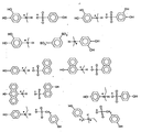
- Y is structure 2, where R 4 is selected from a group consisting of C 1 -C 8 alkyl, aryl, C 1 -C 8 alkylene, arylene, arylene-hydroxyl and mixtures thereof and preferably comprises an arylene-hydroxyl moiety;
- X 4 is a direct valence bond or a C 1 -C 8 alkylene group;
- n 1, 2 or 3; and further where the vinyl ether terminated crosslinking agent is represented by the structure below;
- a C 1 -C 8 unsubstituted or substituted such heterogroups like
- the arylene-hydroxy moiety may be present in R 4 and not in R 1 , R 2 , R 3 .
- the arylene-hydroxy moiety may be present in at least one of R 1 , R 2 , R 3 , and also in R 4 .
- the arylene-hydroxy group may be present only in the anion, only in the cation or in both the anion and cation.
- the arylene-hydroxy moiety is at least one hydroxyl group attached to an aromatic structure arylene (Ar) such as phenyl, naphthyl, anthracyl etc, and the aromatic structure maybe further substituted by C 1 -C 8 alkyl groups. Up to 3 hydroxyl groups may be attached to an arylene group.
- arylene Ar
- the additive aids in the crosslinking of the polymer and the crosslinker.
- the additive of structure (1), where Y is of structure (3) may be used. Further embodiments of the aminium sulfonate are given herein.
- the additive may be represented by structure (10) where n and R 1 , R 2 , R 3 , and R 4 are as described above, where at least one of R 1 , R 2 , R 3 , and R 4 is an arylene-hydroxy group.
- the additive of structure (1) where Y is of structure (2) is used.
- aminium carboxylate additive is given herein.
- the additive may be represented by structure (12), where n and R 1 , R 2 , R 3 , and R 4 are as described above, where at least one of R 1 , R 2 , R 3 , and R 4 is an arylene-hydroxy group.
- both the cation and sulfonate containing anion contain an arylene-hydroxyl moiety.
- both the cation and carboxylate containing anion contain an arylene-hydroxyl moiety.
- the additive may be of structure (10) where R 1 , R 2 , and R 3 , are independently selected from a C 1 -C 8 alkyl group, an aryl moiety (such as shown in structures (7), (8) or (9)), and R 4 is an arylene-hydroxyl moiety which may be chosen from structures (4), (5) or (6).
- the sulfonate ion comprises an arylene-hydroxyl moiety.
- the additive may be of structure (12) where R 1 , R 2 , and R 3 , are independently selected from a C 1 -C 8 alkyl group, an aryl moiety (such as shown in structures (7), (8) or (9)), and R 4 is an arylene-hydroxyl moiety which may be chosen from structures (4), (5) or (6).
- the carboxylate ion comprises an arylene-hydroxyl moiety.
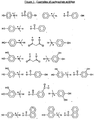
- Figure 1 shows examples of the carboxylate additives.
- Figure 2 shows examples of the sulfonate additives.
- the additive are triethylaminium 4-hydroxybenzenesulfonate, bis[tris(4-vinyloxyethoxyphenyl)sulfonium]perfluorobutanedisulfonate triethylaminium 4-hydroxyphenylacetate, trihexylaminium 4-hydroxyphenylacetate, triethylaminium 3-(4-hydroxyphenyl)propionate, 3-hydroxyphenyl-N,N-dimethylaminium 4-hydroxyphenylacetate, and bis(3-hydroxyphenyl-N,N-dimethylaminium)malonate.
- Alkyl means linear or branched alkyl having the desirable number of carbon atoms and valence.
- the alkyl group is generally aliphatic and may be cyclic or acyclic (i.e. noncyclic). Suitable acyclic groups can be methyl, ethyl, n-or isopropyl, n-,iso, or tert-butyl, linear or branched pentyl, hexyl, heptyl, octyl, decyl, dodecyl, tetradecyl and hexadecyl. Unless otherwise stated, alkyl refers to 1-10 carbon atom moieties.
- the cyclic alkyl groups may be mono cyclic or polycyclic. Suitable example of mono-cyclic alkyl groups include substituted cyclopentyl, cyclohexyl, and cycloheptyl groups. The substituents may be any of the acyclic alkyl groups described herein. Suitable bicyclic alkyl groups include substituted bicyclo[2.2.1]heptane, bicyclo[2.2.2]octane, bicyclo[3.2.1]octane, bicyclo[3.2.2]nonane, and bicyclo[3.3.2]decane, and the like. Examples of tricyclic alkyl groups include tricyclo[5.4.0.0.
- cyclic alkyl groups may have any of the acyclic alkyl groups as substituents.
- Alkylene groups are multivalent alkyl groups derived from any of the alkyl groups mentioned hereinabove. When referring to alkylene groups, these include an alkylene chain substituted with (C 1 -C 6 )alkyl groups in the main carbon chain of the alkylene group. Alkylene groups can also include one or more alkyne groups in the alkylene moiety, where alkyne refers to a triple bond. Essentially an alkylene is a divalent hydrocarbon group as the backbone.
- a divalent acyclic group may be methylene, 1,1- or 1,2-ethylene, 1,1-, 1,2-, or 1,3 propylene, 2,5-dimethyl-hexene, 2,5-dimethyl-hex-3-yne, and so on.
- a divalent cyclic alkyl group may be 1,2- or 1,3-cyclopentylene, 1,2-, 1,3-, or 1,4-cyclohexylene, and the like.
- a divalent tricyclo alkyl groups may be any of the tricyclic alkyl groups mentioned herein above.
- a particularly useful tricyclic alkyl group in this invention is 4,8-bis(methylene)-tricyclo[5.2.1.0. 2,6 ]decane.
- Aryl groups contain 6 to 24 carbon atoms including phenyl, tolyl, xylyl, naphthyl, anthracyl, biphenyls, bis-phenyls, tris-phenyls and the like. These aryl groups may further be substituted with any of the appropriate substituents e.g. alkyl, alkoxy, acyl or aryl groups mentioned hereinabove. Similarly, appropriate polyvalent aryl groups, arylenes, may be used in this invention. Representative examples of divalent aryl groups include phenylenes, xylylenes, naphthylenes, biphenylenes, and the like.
- the novel composition comprises a polymer, a crosslinker and the novel additive.
- the polymer comprises a crosslinkable group.
- the polymer comprises a crosslinkable group and a chromophore.
- the polymers may further comprise an acid labile group.
- Antireflective compositions where the novel additive may be used are described in the following US patents and patent applications and are incorporated herein by reference US 7,824,837 , US 2008/0090184 , US 2010/0119972 , US 2011/0086312 and US application no. 12/944,420 filed November 11, 2010 .
- the coating is baked to form a crosslinked coating which is removed by dry etching but not removed by an aqueous alkaline developer used to image the photoresist.
- the antireflective coating composition comprising a polymer comprising a crosslinkable group and a chromophore, a crosslinker and the novel additive.
- the coating is baked to form a crosslinked coating which is not removed by an aqueous alkaline developer used to image the photoresist. No acid labile groups are formed between the polymer and the crosslinker.
- the polymer may be a crosslinkable polymer.
- the crosslinkable polymer is one or mixture of polymers which comprise reactive groups which can crosslink with the polymer of the present invention.
- Nonlimiting examples of the various types of crosslinkable polymers would be ones which contain functionalities which crosslink, such as acids, alcohols, esters, ethers, etc. Particularly preferred are polymers containing hydroxyl groups, carboxylic acid groups, carboxylic esters, epoxy groups, urethanes and amides.
- Crosslinkable polymers such as, copolymers of polyhydroxystyrene, poly(hydroxynaphthalene), poly(metha)crylates, polyarylates, polyesters, polyurethanes, and alkyd resins(aliphatic polyesters) may be used.
- Useful polymers are exemplified by poly(hydroxystyrene-methylmethacrylate), homopolymers and/or copolymers obtained by polymerization of at least one of the following monomers: styrene, hydroxystyrene, hydroxyethyl(meth)acrylate, hydroxypropyl(meth)acrylate, methyl (meth)acrylate, ethyl (meth)acrylate, (meth)acrylic acid, polymers described in US patents US 6,465,148 , US 5,733,714 , US 6,737,492 , US 6,187,506 , US 5,981,145 and US 2004/0101779 , all of which are incorporated herein by reference.
- crosslinkable polymers are poly(hydroxystyrene-styrene-methacrylate), poly(hydroxystyrene-styrene-methacrylate), poly(4-hydroxystyrene), and poly(pyromellitic dianhydride-ethylene glycol-propylene oxide).
- crosslinking agents can be used in the composition of the present invention. Any suitable crosslinking agents that can crosslink the crosslinkable polymer in the presence of an acid may be used.
- crosslinking agents examples, without limitation, of such crosslinking agents are resins containing melamines, methylols, glycoluril, polymeric glycolurils, benzoguanamine, urea, hydroxy alkyl amides, epoxy and epoxy amine resins, blocked isocyanates, and divinyl monomers.
- Monomeric melamines like hexamethoxymethyl melamine; glycolurils like tetrakis(methoxymethyl)glycoluril; and aromatic methylols, like 2,6 bishydroxymethyl p-cresol may be used.
- crosslinking agents disclosed in US 2006/0058468 and incorporated herein by reference, where the crosslinking agent is a polymeric glycoluril obtained by reacting at least one glycoluril compound with at least one reactive compound containing at least one hydroxy group and/or at least one acid group may be used.
- the additive is any described herein.
- antireflective composition is a positive bottom photoimageable antireflective coating composition developable to form a pattern in this coating using an aqueous alkaline developer
- the composition comprises the novel additive, a crosslinking agent and a polymer, where the polymer comprises at least one hydroxyl and/or a carboxyl group and/or at least one absorbing chromophore.
- the hydroxyl and/or a carboxyl group and the absorbing group may be in the same recurring unit or the polymer comprises at least one recurring unit with a hydroxyl and/or a carboxyl group and at least one recurring unit with an absorbing chromophore.
- the polymer useful for the present embodiment may comprise at least one unit with hydroxyl and/or carboxyl group and at least one unit with an absorbing chromophore.
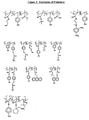
- an absorbing chromophore are hydrocarbon aromatic moieties and heterocyclic aromatic moieties with from one to four separate or fused rings, where there are 3 to 10 atoms in each ring.
- Examples of monomers with absorbing chromophores that can be polymerized are vinyl compounds containing substituted and unsubstituted phenyl, substituted and unsubstituted anthracyl, substituted and unsubstituted phenanthryl, substituted and unsubstituted naphthyl, substituted and unsubstituted heterocyclic rings containing heteroatoms such as oxygen, nitrogen, sulfur, or combinations thereof, such as pyrrolidinyl, pyranyl, piperidinyl, acridinyl, quinolinyl.
- the substituents may be any hydrocarbyl group and may further contain heteroatoms, such as, oxygen, nitrogen, sulfur or combinations thereof.
- Examples of such groups are (C 1 -C 12 ) alkylene, esters, ethers, etc.
- Other chromophores are described in US 6,114,085 , and in US 5,652,297 , US 5,981,145 , US 6,187,506 , US 5,939,236 , and US 5,935,760 , which may also be used, and are incorporated herein by reference.
- the monomers may be vinyl compounds, such as, vinyl ester compounds, vinyl ether compounds, vinyl aromatics, vinyl alkylenearomatic compounds, etc.
- the preferred chromophoric monomers are vinyl compounds of substituted and unsubstituted phenyl, substituted and unsubstituted anthracyl, and substituted and unsubstituted naphthyl; and more preferred monomers are styrene, hydroxystyrene, acetoxystyrene, vinyl benzoate, vinyl 4-tert-butylbenzoate, ethylene glycol phenyl ether acrylate, phenoxypropyl acrylate, N-methyl maleimide, 2-(4-benzoyl-3-hydroxyphenoxy)ethyl acrylate, 2-hydroxy-3-phenoxypropyl acrylate, phenyl methacrylate, phenol methacrylate, benzyl methacrylate, 9-anthracenylmethyl methacrylate, 9-vinylanthracene, 2-vinylnaphthalene, N-vinylphthalimide, N-(3-hydroxy)phenyl methacryl
- any chromophore that absorbs at the appropriate exposure wavelength may be used alone or in combination with other chromophores.
- the substituents may be hydroxyl, alkyl, ester, ether, alkoxycarbonyl, fluoroalcohol, vinyloxyalkylene, etc.
- one function of the polymer is to provide a good coating quality and another is to enable the antireflective coating to change solubility during the imaging process.
- the hydroxyl or carboxyl groups in the polymer provide one of the components necessary for the solubility change.
- Examples of monomers which provide such a unit upon polymerization are without limitations, substituted or unsubstituted vinyl monomers containing a hydroxyl and or carboxyl group, such as acrylic acid, methacrylic acid, vinyl alcohol, hydroxystyrenes, hydroxyethyl methacrylate, hydroxypropyl methacrylate, N-(hydroxymethyl)acrylamide, 4-hydroxyphenyloxy methacrylate, 4-hydroxyphenyloxy acrylate, 5-hydroxynaphthyloxy methacrylate, 5-hydroxynaphthyloxy acrylate, vinyl monomers containing 1,1',2,2',3,3'-hexafluoro-2-propanol, although any monomer that makes the polymer alkali soluble and preferably water insoluble, may be used.
- substituted or unsubstituted vinyl monomers containing a hydroxyl and or carboxyl group such as acrylic acid, methacrylic acid, vinyl alcohol, hydroxystyrenes, hydroxyeth
- the polymer may contain a mixture of monomer units containing hydroxyl and/or carboxyl groups.
- Vinyl monomers containing the 1,1,1,3,3,3-hexafluoro-2-propanol group are represented by structures (14) to (19) and their substituted equivalents.
- a polymer may be synthesized by polymerizing monomers that contain a hydroxyl or carboxyl group with monomers that contain an absorbing chromophore.
- monomers that contain a hydroxyl or carboxyl group with monomers that contain an absorbing chromophore.
- chromophores are useful at the exposure wavelength of interest.
- the alkali soluble polymer may be reacted with compounds that provide the hydroxyl or carboxyl group and compounds that provide the absorbing chromophore.
- the mole % of the unit or units containing the hydroxyl or carboxyl group can range from 5 to 95, preferably 10 to 90, and more preferably 20 to 80 and the mole % of the absorbing chromophore unit in the final polymer can range from 5 to 95, preferably 10 to 90 more preferably 20 to 80. It is also within the scope of this invention that a hydroxyl or carboxyl group is attached to the absorbing chromophore or that the chromophore is attached to the hydroxyl or carboxyl group, that is, both groups are present in the same unit. As an example the chromophoric groups described previously may have pendant hydroxyl and/or carboxyl groups or that the chromophoric groups and the hydroxyl group and/or carbonyl group are attached to the same group.
- the polymer may contain other nonabsorbing monomeric units, such units may provide other desirable properties.
- nonabsorbing monomeric units can be useful at the exposure wavelength of interest.
- Examples of the third monomer include -CR 1 R 2 -CR 3 R 4 -, where R 1 to R 4 are independently H, (C 1 -C 10 ) alkyl, (C 1 -C 10 ) alkoxy, nitro, halide, cyano, alkylaryl, alkenyl, dicyanovinyl, SO 2 CF 3 , COOZ, SO 3 Z, COZ, OZ, NZ 2 , SZ, SO 2 Z, NHCOZ, SO 2 NZ 2 , where Z is H, or (C 1 -C 10 ) alkyl, hydroxy (C 1 -C 10 ) alkyl, (C 1 -C 10 ) alkylOCOCH 2 COCH 3 , or R 2 and R 4 combine to form a cyclic group such as anhydride, pyridine, or pyrollidone, or R 1 to R 3 are independently H, (C 1 -C 10 ) alkyl, (C 1 -C 10 ) alkoxy and
- Other hydrophilic vinyl monomers that can be used to form the polymer are acrylic acid, methacrylic acid, vinyl alcohol, maleic anhydride, maleic acid, maleimide, N-methyl maleimide, N-hydroxymethyl acrylamide and N-vinyl pyrrolidinone.
- monomers may be methyl methacrylate, butyl methacrylate, hydroxyethyl methacrylate and hydroxypropyl methacrylate.
- Monomeric units containing acid labile groups may also be used, such as hydroxystyrene, vinyl alcohol, (meth)acrylic acid capped with acid labile groups.
- acid labile groups are secondary and tertiary alkyls (up to 20 carbon atoms) with at least one ⁇ hydrogen, acetals and ketals, trimethylsilyl, and ⁇ -trimethylsilyl substituted alkyls.
- acid labile groups are tert-butyl, tert-pentyl, isobornyl, 1-alkylcyclohexyl, 1-alkylcyclopentyl, cyclohexyl, 2-alkyl-2-adamantyl, 2-alkyl-2-norbornyl.
- Other examples of acid labile groups are tetrahydrofuranyl tetrahydropyranyl, substituted or unsubstituted methoxycarbonyl, ⁇ -trialkylsilylalkyl groups (e.g. CH 2 -CH 2 Si(CH 3 ) 3 , CH(-CH 2 Si(CH 3 ) 3 ) 2 , CH 2 -CH(Si(CH 3 ) 3 ) 2 ) and the like.
- Examples of monomers containing acid labile groups that can be used in the polymers include methacrylate ester of methyladamantane, methacrylate ester of mevalonic lactone, 3-hydroxy-1-adamantyl methacrylate, methacrylate ester of beta-hydroxy-gamma-butyrolactone, t-butyl norbornyl carboxylate, t-butyl methyl adamantyl methacrylate, methyl adamantyl acrylate, t-butyl acrylate and t-butyl methacrylate; t-butoxy carbonyl oxy vinyl benzene, benzyl oxy carbonyl oxy vinyl benzene; ethoxy ethyl oxy vinyl benzene; trimethyl silyl ether of vinyl phenol, and 2-tris(trimethylsilyl)silyl ethyl ester of methyl methacrylate.
- vinyl ether terminated crosslinking agents include bis(4-vinyloxy butyl) adipate; tris(4-vinyloxybutyl)-1,2,5-cyclohexanetricarboxylate, bis(4-vinyloxy butyl) succinate; bis(4-vinyloxy butyl) isophathalate; bis(4-vinyloxymethyl cyclohexylmethyl) glutarate; tris(4-vinyloxy butyl) trimellitate; bis(4-vinyloxy methyl cyclohexyl methyl) terephthalate; bis(4-vinyloxy methyl cyclohexyl methyl) isophthalate; bis(4-vinyloxy butyl) (4-methyl-1,3-phenylene) biscarbamate; bis(4-vinyloxy butyl) (methylene di-4,1-phenylene) biscarbamate; and triethyleneglycol divinylether, 1,4-cyclo
- Vinyl ether terminated crosslinking agents are described in T. Yamaoka, et al., Trends in Photochem. Photobio., 7:45 (2001 ); S. Moon, et al., Chem. Mater., 6:1854 (1994 ); or H. Schacht, et al., ACS Symp. Ser. 706:78 (1998 ) which may also be used, and are incorporated herein by reference.
- Vinyl ether crosslinkers crosslink with the polymer to provide an acid labile structure which is capable of being decrosslinked in the presence of an acid, which are particularly useful for photoimageable antireflective coating compositions.
- the vinyl ether terminated crosslinking agent is added to the antireflective coating in a proportion which provides 0.20-2.00 mol equivalents of vinyl ether crosslinking function per reactive group on the polymer, or 0.50-1.50 reactive equivalents per reactive group.
- the antireflective coating composition comprises a an optional photoacid generator
- the photoacid generator in the antireflective coating and the photoacid generator in the photoresist are sensitive to the same wavelength of light, and thus the same radiant wavelength of light can cause an acid to be formed in both layers.
- the acid in the exposed areas of the antireflective coating present either through diffusion from the photoresist or through photogeneration from the photoacid generator in the antireflective film, reacts with the acid labile crosslinkages to decrosslink the polymer, thus making the exposed areas of the antireflective coating soluble in the aqueous alkaline developer.
- the photoacid generator of the antireflective coating chosen depends on the photoresist to be used.
- the photoacid generator (PAG) of the novel composition is selected from those which absorb at the desired exposure wavelength, preferably 248 nm, 193 nm and 157 nm for deep ultraviolet photoresists, 13.5 nm for extreme ultraviolet, and naphthoquinone diazides or sulfonium salts for 365 nm, 436 nm and broadband photoresists.
- Suitable examples of the acid generating photosensitive compounds include, without limitation, ionic photoacid generators (PAG), such as diazonium salts, iodonium salts, sulfonium salts, or non-ionic PAGs such as diazosulfonyl compounds, sulfonyloxy imides, and nitrobenzyl sulfonate esters, although any photosensitive compound that produces an acid upon irradiation may be used.
- PAG ionic photoacid generators
- the onium salts are usually used in a form soluble in organic solvents, mostly as iodonium or sulfonium salts, examples of which are diphenyliodonium trifluoromethane sulfonate, diphenyliodonium nonafluorobutane sulfonate, triphenylsulfonium trifluromethane sulfonate, triphenylsulfonium nonafluorobutane sulfonate and the like.
- Other compounds that form an acid upon irradiation are triazines, oxazoles, oxadiazoles, thiazoles, substituted 2-pyrones.
- Phenolic sulfonic esters bis-sulfonylmethanes, bis-sulfonylmethanes or bis-sulfonyldiazomethanes, triphenylsulfonium tris(trifluoromethylsulfonyl)methide, triphenylsulfonium bis(trifluoromethylsulfonyl)imide, diphenyliodonium tris(trifluoromethylsulfonyl)methide, diphenyliodonium bis(trifluoromethylsulfonyl)imide and their homologues are also possible candidates. Mixtures of photoactive compounds may also be used.
- the antireflective coating composition comprises an optional photoacid generator which comprises vinyl ether groups, which can act as a crosslinker reacting with hydroxyl moieties. Examples of such crosslinkers are given in US 2010/0119972 .
- the solvent for the antireflective coating is chosen such that it can dissolve all the solid components of the antireflective coating.
- suitable solvents for the antireflective coating composition are cyclohexanone, cyclopentanone, anisole, 2-heptanone, ethyl lactate, propylene glycol monomethyl ether acetate, propylene glycol monomethyl ether, butyl acetate, gamma butyroacetate, ethyl cellosolve acetate, methyl cellosolve acetate, methyl 3-methoxypropionate, ethyl pyruvate, 2-methoxybutyl acetate, diacetone alcohol, diethyl carbonate, 2-methoxyethyl ether, but ethyl lactate, propylene glycol monomethyl ether acetate, propylene glycol monomethyl ether or mixtures thereof are preferred. Solvents with a lower degree of toxicity and good coating and solubility properties are generally preferred.
- composition of the present invention may further comprise an additional additive such as thermal acid generator which does not contain any hydroxyarylene moieties.
- thermal acid generator Any known thermal acid generators may be used, exemplified without limitations, by 2,4,4,6-tetrabromocyclohexadienone, benzoin tosylate, squaric acid, 2-nitrobenzyl tosylate, chloroacetic acid, toluenesulfonic acid, methanesulfonic acid, nonaflate acid, triflic acid, other alkyl esters of organic sulfonic acids, salts of these mentioned acids.
- the thermal acid generator may be a component that releases an acid of moderate acidity, i.e.
- a thermal acid generator that releases acids with a pKa of less than 5.0 and greater than 1.0 are also preferred.
- acids or acids derived from thermal acid generators with moderate acidity are maleic acid (pKa of 1.83), chloroacetic acid (pKa of 1.4), dichloroacetic acid (pKa of 1.48), oxalic acid (pKa of 1.3), cinnamic acid (pKa of 4.45), tartaric acid (pKa of 4.3), gylcolic acid (pKa of 3.8), fumaric acid (pKa of 4.45), malonic acid (pKa of 2.8), cyanoacetic acid (pKa of 2.7), etc.
- Acids which are blocked by bases to form a thermal acid generator are preferred. Acids, such as those described above, may be blocked with bases such as amines.
- Typical bases are triethyl amine, tripropyl amine, trimethyl amine, tributyl amine, tripentyl amine, tridodecyl amine etc. Additionally, diaryl or trialkyl sulfonium salts with anions of weak acids, such as carboxylic acid or aryl carboxylic acid may be used. Acids which are blocked by bases may be formed by combining the acid with a base, where the acid:base ratio ranges from about 1:1 to about 1:3.
- the additives may be present in the antireflective composition at levels ranging from 0.1 to 25 weight% of solids, especially 0.1 to about 5 weight%.
- thermal acid generators that release acids with a pKa of less than 1.0 are also preferred.
- acids or acids derived from thermal acid generators with strong acidity are toluenesulfonic acid, octanesulfonic acid, triflic acid, perfluorobutanesulfonic acid etc.
- Acids which are blocked by bases to form a thermal acid generator are preferred. Acids, such as those described above, may be blocked with bases such as amines.
- Typical bases are triethyl amine, tripropyl amine, trimethyl amine, tributyl amine, tripentyl amine, tridodecyl amine etc. Additionally, diaryl or trialkyl sulfonium salts with anions of strong acid, such as arylsulfonic acid, alkyl sulfonic acid or perfluoroalkyl sulfonic acid may be used. Acids which are blocked by bases may be formed by combining the acid with a base, where the acid:base ratio ranges from about 1:1 to about 1:3. The additives may be present in the antireflective composition at levels ranging from 0.1 to 25 weight% of solids, especially 0.1 to about 5 weight%.
- the antireflective coating compositions of the present invention may comprise up to about 15 percent by weight of the solids, preferably less than 8 percent, based on the total weight of the coating composition.
- the solids may comprise from 1 to 15 weight percent of the novel additive having structure 1, 0.5 to 25 weight percent of the optional photoacid generator, 0.5 to 25 weight percent of the optional crosslinking photoacid generators, 50 to 99 weight percent of polymer, 1 to 50 weight percent of the crosslinking agent and optionally 0.1 to 10 weight percent of additional thermal acid generator, based on the total solids content of the antireflective coating composition.
- the photoacid generator level ranges from about 0.01 to about 20 weight%.
- the novel additive ranges from about 0.1 to 10 weight percent of the total solids
- the crosslinking agent ranges from about 5 to about 40 weight percent or 10 to 35 weight percent of the total solids.
- the solid components are dissolved in the solvent, or mixtures of solvents, and filtered to remove impurities.
- the components of the antireflective coating may also be treated by techniques such as passing through an ion exchange column, filtration, and extraction process, to improve the quality of the product.
- additives may be present at up to 30 weight percent level.
- Other polymers such as, novolaks, polyhydroxystyrene, polymethylmethacrylate and polyarylates, may be added to the composition, providing the performance is not negatively impacted.
- the amount of this polymer is kept below 50 weight % of the total solids of the composition, more preferably 35 weight %, and even more preferably below 20 weight %.
- Bases may also be added to the composition to enhance stability. Both photobases and nonphotobases are known additives.
- bases are tetramethylammonium carboxylate salts, amines, ammonium hydroxide, and photosensitive bases.
- Particularly preferred bases are tetrabutylammonium hydroxide, triethanolamine, diethanol amine, trioctylamine, n-octylamine, trimethylsulfonium hydroxide, triphenylsulfonium hydroxide, bis(t-butylphenyl)iodonium cyclamate and tris(tert-butylphenyl)sulfonium cyclamate, tetramethylammonium deoxycholate, tetramethylammonium cholate, tetramethylammonium lithocholate and in general amine bases having a boiling point above 130°C.
- the absorption parameter (k) of the novel composition ranges from about 0.1 to about 1.0, preferably from about 0.15 to about 0.7 as measured using ellipsometry.
- the refractive index (n) of the antireflective coating is also optimized.
- the n and k values can be calculated using an ellipsometer, such as the J. A. Woollam WVASE VU-302 TM Ellipsometer.
- the exact values of the optimum ranges for k and n are dependent on the exposure wavelength used and the type of application. Typically for 193 nm the preferred range for k is 0.1 to 0.75, for 248 nm the preferred range for k is 0.15 to 0.8, and for 365 nm the preferred range is from 0.1 to 0.8.
- the thickness of the antireflective coating is less than the thickness of the top photoresist.
- the film thickness of the antireflective coating is less than the value of (wavelength of exposure/refractive index), and more preferably it is less than the value of
- the optimum film thickness of the antireflective coating is determined by the exposure wavelength, refractive indices of the antireflective coating and of the photoresist, absorption characteristics of the top and bottom coatings, and optical characteristics of the substrate. In this case, since the bottom antireflective coating is removed by exposure and development steps, the optimum film thickness is determined by avoiding the optical nodes where no light absorption is present in the antireflective coating.
- the antireflective coating composition is coated on the substrate using techniques well known to those skilled in the art, such as dipping, spin coating or spraying.
- Various substrates known in the art may be used, such as those that are planar, have topography or have holes.
- semiconductor substrates are crystalline and polycrystalline silicon, silicon dioxide, silicon (oxy)nitride, aluminum, aluminum/silicon alloys, and tungsten.
- edge bead there can be a buildup of photoresist film at the edges of the substrate, referred to as edge bead.
- This edge bead can be removed using a solvent or mixture of solvents using techniques well known to those of ordinary skill in the art.
- the composition of the present invention is particularly compatible with edge bead removers.
- Typical solvents used for edge bead removers are ethyl lactate, butyl acetate, propyleneglycol monomethyletheracetate, propyleneglycol monomethylether, or mixtures thereof.
- the coating is then cured.
- the preferred range of temperature is from about 120°C to about 240°C for about 30-120 seconds on a hot plate or equivalent heating unit, more preferably from about 150°C to about 200°C for 45-90 seconds.
- the film thickness of the antireflective coating ranges from about 20 nm to about 300 nm. The optimum film thickness is determined, as is well known in the art, to be where good lithographic properties are obtained, especially where no standing waves are observed in the photoresist.
- Positive photoresists which are developed with aqueous alkaline solutions, are useful for the present invention, provided the photoactive compounds in the photoresist and the antireflective coating absorb at the same exposure wavelength used for the imaging process for the photoresist.
- Positive-working photoresist compositions are exposed image-wise to radiation, those areas of the photoresist composition exposed to the radiation become more soluble to the developer solution while those areas not exposed remain relatively insoluble to the developer solution.
- treatment of an exposed positive-working photoresist with the developer causes removal of the exposed areas of the coating and the formation of a positive image in the photoresist coating.
- Photoresist resolution is defined as the smallest feature which the resist composition can transfer from the photomask to the substrate with a high degree of image edge acuity after exposure and development. In many manufacturing applications today, resist resolution on the order of less than one micron are necessary. In addition, it is almost always desirable that the developed photoresist wall profiles be near vertical relative to the substrate. Such demarcations between developed and undeveloped areas of the resist coating translate into accurate pattern transfer of the mask image onto the substrate. This becomes even more critical as the drive toward miniaturization reduces the critical dimensions on the devices.
- Photoresists can be any of the types used in the semiconductor industry, provided the photoactive compound in the photoresist and the antireflective coating absorb at the exposure wavelength used for the imaging process.
- Photoresists for 248 nm have typically been based on substituted polyhydroxystyrene and its copolymers/onium salts, such as those described in US 4,491,628 and US 5,350,660 .
- photoresists for exposure below 200 nm require non-aromatic polymers since aromatics are opaque at this wavelength.
- US 5,843,624 and US 6,866,984 disclose photoresists useful for 193 nm exposure.
- polymers containing alicyclic hydrocarbons are used for photoresists for exposure below 200 nm.
- Alicyclic hydrocarbons are incorporated into the polymer for many reasons, primarily since they have relatively high carbon to hydrogen ratios which improve etch resistance, they also provide transparency at low wavelengths and they have relatively high glass transition temperatures.
- US 5,843,624 discloses polymers for photoresist that are obtained by free radical polymerization of maleic anhydride and unsaturated cyclic monomers. Any of the known types of 193nm photoresists may be used, such as those described in US 6,447,980 and US 6,723,488 , and incorporated herein by reference.
- One class of 157 nm fluoroalcohol photoresists is derived from polymers containing groups such as fluorinated-norbornenes, and are homopolymerized or copolymerized with other transparent monomers such as tetrafluoroethylene ( US 6,790,587 , and US 6,849,377 ) using either metal catalyzed or radical polymerization. Generally, these materials give higher absorbencies but have good plasma etch resistance due to their high alicyclic content.
- a film of photoresist is then coated on top of the cured antireflective coating and baked to substantially remove the photoresist solvent.
- the photoresist is imagewise exposed to actinic radiation and then developed to form an image in the photoresist pattern, without transferring the pattern into the antireflective coating film.
- dry etching is used to remove the novel antireflective film.
- the photoresist and the antireflective coating bilevel layers are then imagewise exposed to actinic radiation.
- the acid generated during exposure step reacts to de-crosslink the polymer of the antireflective coating composition and thus rendering the exposed region of the antireflective coating alkali soluble in the developing solution.
- the temperature for the postexposure bake step can range from 40°C to 200°C for 30-200 seconds on a hot plate or equivalent heating system, preferably from 80°C to 160°C for 40-90 seconds. In some instances, it is possible to avoid the postexposure bake, since for certain chemistries, such as some acetal acid labile linkages, deprotection proceeds at room temperature.
- the polymer in the exposed regions of the antireflective coating is now soluble in an aqueous alkaline solution.
- the bilevel system is then developed in an aqueous alkaline developer to remove the photoresist and the antireflective coating.
- the developer is preferably an aqueous alkaline solution comprising, for example, tetramethyl ammonium hydroxide.
- the developer may further comprise additives, such as surfactants, polymers, isopropanol, ethanol, etc.
- the process of coating and imaging photoresist coatings and antireflective coatings is well known to those skilled in the art and is optimized for the specific type of photoresist and antireflective coating combination used.
- the imaged bilevel system can then be processed further as required by the manufacturing process of integrated circuits, for example metal deposition and etching.
- the absorption parameter (k) and the refractive index (n) were measured using variable angle spectrophotometric ellipsometry.
- the bottom antireflective coating (B.A.R.C.) solutions were spin coated on primed silicon wafers and baked to get a given film thickness. The coated wafers were then measured using an ellipsometer manufactured by J.A. Woollam or Sopra Corporation. The obtained data were fitted to get the k and n values of the B.A.R.C. films.
- Polymers were obtained by radical polymerization using the general procedure outlined in US 2011/0076626 .
- the number in the parenthesis for each polymer represents the molar feed ratio of monomers used when employing this procedure.
- the photoresist used was any one of commercially available 193 nm or 248 nm photoresist sold by vendors such as Sumitomo Chemical, Tokyo Ohka and Japan Synthetic Rubber.
- the solvent used as a prewet solvent for photoresist coating is any of PGMEA, PGME, ethyl lactate, cyclohexane, n-butyl acetate, ⁇ -butyrolactone and mixture thereof.
- Table 1 lists examples 1-15 which were all the salts which were made as stock solutions in PGME and used in the formulation examples. These were reacted in the same manner as shown above, but leaving the materials in PGME as stock solutions to be used in the above described formulation examples. Table 1 Synth.
- the B.A.R.C. solution was coated on a silicon wafer and heated on a hotplate at 190°C for 60 seconds to give a film thickness of 400 ⁇ .
- the absorption (k) value was 0.38 and the refractive index (n) value was 1.726 at 193 nm.
- the B.A.R.C. wafer was prewet with a solvent and coated with 193nm photoresist and heated on a hotplate for 110°C for 60 seconds to give a film thickness of 140 nm.
- the coated wafer was exposed using Nikon 306D 193 nm scanner for imagewise exposure through a mask.
- the exposed wafer was then post exposure baked for 60 seconds at 110°C and followed with a 30 second puddle development at 23°C using of AZ® 300 MIF Developer (2.38wt% TMAH aqueous solution available from AZ Electronic Materials USA Corp., 70 Meister Ave., Somerville NJ).
- AZ® 300 MIF Developer 2.38wt% TMAH aqueous solution available from AZ Electronic Materials USA Corp., 70 Meister Ave., Somerville NJ.
- SEM Scanning Electron Microscope
- 125 nm photoresist/B.A.R.C. Lines (1:1) were obtained with clean pattern for resist and clean trench spaces with complete opening of the B.A.R.C. pattern at a dose of 20.0 mJ/cm 2 . Pattern collapse was not observed up to and including 26 mJ/cm 2 .
- PQMA/EAdMA (60/40) copolymer (0.197g), tris(vinyloxybutyl)cyclohexane 1,2,4-tricarboxylate (0.0579g), trihexylaminium 4-hydroxyphenylacetate (0.0991 g) and bis[tris(4-vinyloxyethoxyphenyl)sulfonium]perfluorobutanedisulfonate (0.0058g) were dissolved in a mixture of 13.57g of propyleneglycol monomethylether, 5.81 g of propyleneglycol monomethylether acetate and 0.241g of ⁇ -valerolactone to form a antireflective composition (B.A.R.C. solution). The solution was filtered through a 0.2 ⁇ m micron filter.
- the B.A.R.C. solution was coated on a silicon wafer and heated on a hotplate at 190°C for 60 seconds to give a film thickness of 400 ⁇ .
- the absorption (k) value was 0.387 and the refractive index (n) value was 1.728 at 193 nm.
- the B.A.R.C. wafer was prewet with a solvent and coated with 193nm photoresist heated on a hotplate for 130°C for 60 seconds to give a film thickness of 140 nm.
- the coated wafer was exposed using Nikon 306D 193 nm scanner for imagewise exposure.
- the exposed wafer was then post exposure baked for 60 seconds at 105°C and followed with a 30 second puddle development at 23°C using of AZ® 300 MIF Developer.
- SEM Scanning Electron Microscope
- PQMA/EAdMA (60/40) copolymer (0.658g), tris(vinyloxybutyl)cyclohexane 1,2,4-tricarboxylate (0.198g), triethylaminium 3-(4-hydroxyphenyl)propionate (0.210g) and bis[tris(4-vinyloxyethoxyphenyl)sulfoniumlperfluorobutanedisulfonate (0.0139g) were dissolved in a mixture of 40.73g of propyleneglycol monomethylether, 17.45 g of propyleneglycol monomethylether acetate and 0.724g of ⁇ -valerolactone to form a antireflective composition (B.A.R.C. solution). The solution was filtered through a 0.2 ⁇ m micron filter.
- the B.A.R.C. solution was coated on a silicon wafer, and processed as described in Formulation and Exposure Example 2. Using a scanning electron microscope (SEM), 125 nm photoresist/B.A.R.C. Lines (1:1) were obtained with clean pattern for resist and clean trench spaces with complete opening of the B.A.R.C. pattern at a dose of 23.0 mJ/cm 2 . Pattern collapse was not observed up to and including 27.0 mJ/cm 2 .
- SEM scanning electron microscope
- PQMA/EAdMA (60/40) copolymer (0.658g, tris(vinyloxybutyl)cyclohexane 1,2,4-tricarboxylate (0.193g), triethylaminium 3-(4-hydroxyphenyl)propionate (0.210g) and bis[tris(4-vinyloxyethoxyphenyl)sulfonium]perfluorobutanedisulfonate (0.0194g) were dissolved in a mixture of 40.74g of propyleneglycol monomethylether, 17.45 g of propyleneglycol monomethylether acetate and 0.724g of ⁇ -valerolactone to form a antireflective composition (B.A.R.C. solution). The solution was filtered through a 0.2 ⁇ m micron filter.
- the B.A.R.C. solution was coated on a silicon wafer, and processed as described in Formulation and Exposure Example 2. Using a scanning electron microscope (SEM), 125 nm photoresist/B.A.R.C. Lines (1:1) were obtained with clean pattern for resist and clean trench spaces with complete opening of the B.A.R.C. pattern at a dose of 23.0 mJ/cm2. Pattern collapse was not observed up to and including 27.0 mJ/cm 2 .
- SEM scanning electron microscope
- PQMA/AdOMMA/EAdMA 55/20/25) terpolymer (0.146g), tris(vinyloxybutyl)cyclohexane 1,2,4-tricarboxylate (0.045g), trihexylaminium 4-hydroxyphenylacetate (0.076g) and bis[tris(4-vinyloxyethoxyphenyl)sulfonium]perfluorobutanedisulfonate (0.0031 g) were dissolved in a mixture of 13.64g of propyleneglycol monomethylether, 5.85 g of propyleneglycol monomethylether acetate and 0.247g of ⁇ -valerolactone to form an antireflective composition (B.A.R.C. solution). The solution was filtered through a 0.2 ⁇ m micron filter.
- the B.A.R.C. solution was coated on a silicon wafer, and processed as described in Formulation and Exposure Example 2. Using a scanning electron microscope (SEM), 125 nm photoresist/B.A.R.C. Lines (1:1) were obtained with clean pattern for resist and clean trench spaces with complete opening of the B.A.R.C. pattern at a dose of 23.0 mJ/cm 2 . Pattern collapse was not observed up to and including 27.0 mJ/cm 2 .
- SEM scanning electron microscope
- PQMA/AdOMMA/EAdMA 55/20/25) terpolymer (0.164g), tris(vinyloxybutyl)cyclohexane 1,2,4-tricarboxylate (0.051g), triethylaminium 4-hydroxyphenylacetate (0.051 g) and bis[tris(4-vinyloxyethoxyphenyl)sulfonium]perfluorobutanedisulfonate (0.0035g) were dissolved in a mixture of 13.64g of propyleneglycol monomethylether, 5.85 g of propyleneglycol monomethylether acetate and 0.247g of ⁇ -valerolactone to form an antireflective composition (B.A.R.C. solution). The solution was filtered through a 0.2 ⁇ m micron filter.
- the B.A.R.C. solution was coated on a silicon wafer, and processed as described in Formulation and Exposure Example 2. Using a scanning electron microscope (SEM), 125 nm photoresist/B.A.R.C. Lines (1:1) were obtained with clean pattern for resist and clean trench spaces with complete opening of the B.A.R.C. pattern of 23.0 mJ/cm 2 . Pattern collapse was not observed up to and including 27.0.mJ/cm 2 .
- SEM scanning electron microscope
- the B.A.R.C. solution was coated on a silicon wafer, and processed as described in Formulation and Exposure Example 1. Using a scanning electron microscope (SEM), 125 nm photoresist/B.A.R.C. Lines (1:1) were obtained with clean pattern for resist and clean trench spaces with complete opening of the B.A.R.C. pattern at a dose of 20.0 mJ/cm 2 . Pattern collapse was not observed up to and including 27 mJ/cm 2 .
- SEM scanning electron microscope
- PQMA/AdOMMA/EAdMA 55/20/25) terpolymer (0.171g), tris(vinyloxybutyl)cyclohexane 1,2,4-tricarboxylate (0.050g), bis(3-hydroxyphenyl-N,N-dimethylaminium)malonate (0.044g) and bis[tris(4-vinyloxyethoxyphenyl)sulfonium]perfluorobutanedisulfonate (0.0050g) were dissolved in mixture of 13.64g of propyleneglycol monomethylether, 5.84 g of propyleneglycol monomethylether acetate and 0.25g of ⁇ -valerolactone to form an antireflective composition (B.A.R.C. solution). The solution was filtered through a 0.2 ⁇ m micron filter.
- the B.A.R.C. solution was coated on a silicon wafer, and processed as described in Formulation and Exposure Example 2. Using a scanning electron microscope (SEM), 125 nm photoresist/B.A.R.C. Lines (1:1) were obtained with clean pattern for resist and clean trench spaces with complete opening of the B.A.R.C. pattern at a dose of 23.0 mJ/cm 2 . Pattern collapse was not observed up to and including 27.0 mJ/cm 2 .
- SEM scanning electron microscope
- PQMA/AdOMMA/EAdMA 55/20/25) terpolymer (0.160g), tris(vinyloxybutyl)cyclohexane 1,2,4-tricarboxylate (0.049g), 3-hydroxyphenyl-N,N-dimethylaminium 4- hydroxyphenylacetate (0.057g) and bis[tris(4-vinyloxyethoxyphenyl)sulfonium]perfluorobutanedisulfonate (0.0047g) were dissolved in a mixture of 13.63g of propyleneglycol monomethylether, 5.84 g of propyleneglycol monomethylether acetate and 0.25g of ⁇ -valerolactone to form an antireflective composition (B.A.R.C. solution). The solution was filtered through a 0.2 ⁇ m micron filter.
- the B.A.R.C. solution was coated on a silicon wafer, and processed as described in Formulation and Exposure Example 2. Using a scanning electron microscope (SEM), 125 nm photoresist/B.A.R.C. Lines (1:1) were obtained with clean pattern for resist and clean trench spaces with complete opening of the B.A.R.C. pattern at a dose of 23.0 mJ/cm 2 . Pattern collapse was not observed up to and including 27.0 mJ/cm 2 .
- SEM scanning electron microscope
- PQMA/EAdMA (60/40) copolymer (0.232g), tris(vinyloxybutyl)cyclohexane 1,2,4-tricarboxylate (0.068g), bis(3-hydroxyphenyl-N,N-dimethylaminium)malonate (0.0530g) and bis[tris(4-vinyloxyethoxyphenyl)sulfonium]perfluorobutanedisulfonate (0.0068g) were dissolved in a mixture of 13.58g of propyleneglycol monomethylether, 5.81 g of propyleneglycol monomethylether acetate and 0.241g of ⁇ -valerolactone to form a photosensitive antireflective composition. The B.A.R.C. solution was filtered through a 0.2 ⁇ m micron filter.
- the B.A.R.C. solution was coated on a silicon wafer, and processed as described in Formulation and Exposure Example 1. Using a scanning electron microscope (SEM), 125 nm photoresist/B.A.R.C. Lines (1:1) were obtained with clean pattern for resist and clean trench spaces with complete opening of the B.A.R.C. pattern at a dose of 20.0 mJ/cm 2 . Pattern collapse was not observed up to and including 27 mJ/cm 2 .
- SEM scanning electron microscope
- PQMA/EAdMA (60/40) copolymer (0.215g), tris(vinyloxybutyl)cyclohexane 1,2,4-tricarboxylate (0.063g), 3-hydroxyphenyl-N,N-dimethylaminium 4-hydroxyphenylacetate (0.0745g) and bis[tris(4-vinyloxyethoxyphenyl)sulfonium]perfluorobutanedisulfonate (0.0064g) were dissolved in mixture of 13.58g of propyleneglycol monomethylether, 5.81 g of propyleneglycol monomethylether acetate and 0.241g of ⁇ -valerolactone to form a photosensitive antireflective composition.
- the B.A.R.C. solution was filtered through a 0.2 ⁇ m micron filter.
- the B.A.R.C. solution was coated on a silicon wafer, and processed as described in Formulation and Exposure Example 1. Using a scanning electron microscope (SEM), 125 nm photoresist/B.A.R.C. Lines (1:1) were obtained with clean pattern for resist and clean trench spaces with complete opening of the B.A.R.C. pattern at a dose of 20.0 mJ/cm 2 . Pattern collapse was not observed up to and including 27 mJ/cm 2 .
- SEM scanning electron microscope
- PQMA/EAdMA (60/40) copolymer (0.232g), tris(vinyloxybutyl)cyclohexane 1,2,4-tricarboxylate (0.0683g), bis(3-hydroxyphenyl-N,N-dimethylaminium) malonate (0.0525g) and bis[tris(4-vinyloxyethoxyphenyl)sulfonium]perfluorobutanedisulfonate (0.0068g) were dissolved in a mixture of 13.58g of propyleneglycol monomethylether, 5.81 g of propyleneglycol monomethylether acetate and 0.241 g of ⁇ -valerolactone to form an antireflective composition (B.A.R.C. solution). The solution was filtered through a 0.2 ⁇ m micron filter.
- the B.A.R.C. solution was coated on a silicon wafer, and processed as described in Formulation and Exposure Example 1. Using a scanning electron microscope (SEM), 125 nm photoresist/B.A.R.C. Lines (1:1) were obtained with clean pattern for resist and clean trench spaces with complete opening of the B.A.R.C. pattern at a dose of 20.0 mJ/cm 2 . Pattern collapse was not observed up to and including 27 mJ/cm 2 .
- SEM scanning electron microscope
- the B.A.R.C. solution was coated on a silicon wafer, and processed as described in Example 1. Using a scanning electron microscope (SEM), clean 80 nm photoresist. lines (1:1) were obtained on B.A.R.C. film at a dose of 25.5 mJ/cm 2 . The B.A.R.C. film was not removed after development with the aqueous alkaline developer.
- SEM scanning electron microscope
- the B.A.R.C. solution was coated on a silicon wafer, and processed as described in Example 1. Using a scanning electron microscope (SEM), clean 80 nm photoresist Lines (1:1) were obtained on the B.A.R.C. film at a dose of 25.5 mJ/cm 2 . The B.A.R.C. coating was not developed by the aqueous alkaline developer.
- the B.A.R.C. solution is coated on a silicon wafer and heated on a hotplate at 180°C for 60 seconds to give a film thickness of about 600 ⁇ .
- the B.A.R.C. wafer is prewet with a solvent and coated with a commercially available 248nm photoresist and heated on a hotplate for 95°C for 90 seconds to give a film thickness of about 200nm.
- the coated wafer is exposed using Canon FPA3000EX5 248 nm stepper for imagewise exposure through a mask.
- the exposed wafer is then post exposure baked for 90 seconds at 105°C and followed with a 60 second puddle development at 23°C using of AZ® 300 MIF Developer (2.38wt% TMAH aqueous solution available from AZ Electronic Materials USA Corp., 70 Meister Ave., Somerville NJ).
- AZ® 300 MIF Developer (2.38wt% TMAH aqueous solution available from AZ Electronic Materials USA Corp., 70 Meister Ave., Somerville NJ.
- SEM Scanning Electron Microscope
- PQMA/EAdMA (60/40) copolymer (0.2394g), tris(vinyloxybutyl)cyclohexane 1,2,4-tricarboxylate (0.0718g), bis(triethylaminium)malonate (0.0438g) and bis[tris(4-vinyloxyethoxyphenyl)sulfonium]perfluorobutanedisulfonate (0.0050g) were dissolved in mixture of 13.57g of propyleneglycol monomethylether, 5.81 g of propyleneglycol monomethylether acetate and 0.241 g of ⁇ -valerolactone to form an antireflective composition (B.A.R.C. solution).
- the solution was filtered through a 0.2 ⁇ m micron filter.
- the B.A.R.C. solution was coated on a silicon wafer, and processed as described in Formulation and Exposure Example 1. Using a Scanning Electron Microscope (SEM), patterns were inspected, but 125 nm photoresist/B.A.R.C. Lines (1:1) showed scum and B.A.R.C. was not completely dissolved at dose to print (20mJ/cm 2 ).
- SEM Scanning Electron Microscope
- PQMA/EAdMA (60/40) copolymer (0.2336g), tris(vinyloxybutyl)cyclohexane 1,2,4-tricarboxylate (0.0701g), Bis(triethylaminium)terephthalate (0.0514g) and bis[tris(4-vinyloxyethoxyphenyl)sulfonium]perfluorobutanedisulfonate (0.0049) were dissolved in a mixture of 13.58g of propyleneglycol monomethylether, 5.82 g of propyleneglycol monomethylether acetate and 0.241 g of ⁇ -valerolactone to form an antireflective composition (B.A.R.C. solution).
- the solution was filtered through a 0.2 ⁇ m micron filter.
- the B.A.R.C. solution was coated on a silicon wafer, and processed as described in Formulation and Exposure Example 2.
- SEM Scanning Electron Microscope
- PQMA/EAdMA (60/40) copolymer (0.2331g), tris(vinyloxybutyl)cyclohexane 1,2,4-tricarboxylate (0.0699g), bis(triethylaminium) cyclohexane-3,4-dicarboxylate (0.0521 g) and bis[tris(4-vinyloxyethoxyphenyl)sulfonium]perfluorobutanedisulfonate (0.0049g) were dissolved in mixture of 13.58g of propyleneglycol monomethylether, 5.82 g of propyleneglycol monomethylether acetate and 0.241g of ⁇ -valerolactone to form an antireflective composition (B.A.R.C.
- PQMA/EAdMA (60/40) copolymer (0.209g), tris(vinyloxybutyl)cyclohexane 1,2,4-tricarboxylate (0.0558g), bis(triethylaminium)malonate (0.0323g) and bis(triphenylsulfonium)perfluorobutanedisulfonate (0.0023g) were dissolved in mixture of 24.68g of propyleneglycol monomethylether and 0.0203g of ⁇ -valerolactone to form an antireflective composition (B.A.R.C. solution). The solution was filtered through a 0.2 ⁇ m micron filter.
- the B.A.R.C. solution was coated on a silicon wafer, and processed as described in Example 1. Using a Scanning Electron Microscope (SEM), patterns were inspected, but 125 nm photoresist/B.A.R.C. Lines (1:1) showed scum and B.A.R.C. was not completely dissolved at dose to print (20mJ/cm 2 ).
- SEM Scanning Electron Microscope
Landscapes
- Engineering & Computer Science (AREA)
- Chemical & Material Sciences (AREA)
- Physics & Mathematics (AREA)
- General Physics & Mathematics (AREA)
- Organic Chemistry (AREA)
- Life Sciences & Earth Sciences (AREA)
- Materials Engineering (AREA)
- Wood Science & Technology (AREA)
- Structural Engineering (AREA)
- Architecture (AREA)
- Optics & Photonics (AREA)
- Condensed Matter Physics & Semiconductors (AREA)
- Manufacturing & Machinery (AREA)
- Computer Hardware Design (AREA)
- Microelectronics & Electronic Packaging (AREA)
- Power Engineering (AREA)
- Exposure Of Semiconductors, Excluding Electron Or Ion Beam Exposure (AREA)
- Paints Or Removers (AREA)
- Addition Polymer Or Copolymer, Post-Treatments, Or Chemical Modifications (AREA)
- Materials For Photolithography (AREA)
- Organic Low-Molecular-Weight Compounds And Preparation Thereof (AREA)
Applications Claiming Priority (2)
| Application Number | Priority Date | Filing Date | Title |
|---|---|---|---|
| US13/153,765 US8623589B2 (en) | 2011-06-06 | 2011-06-06 | Bottom antireflective coating compositions and processes thereof |
| PCT/IB2012/001117 WO2012168785A1 (en) | 2011-06-06 | 2012-06-05 | Bottom antireflective coating compositions and processes thereof |
Publications (2)
| Publication Number | Publication Date |
|---|---|
| EP2718379A1 EP2718379A1 (en) | 2014-04-16 |
| EP2718379B1 true EP2718379B1 (en) | 2016-08-17 |
Family
ID=46420459
Family Applications (1)
| Application Number | Title | Priority Date | Filing Date |
|---|---|---|---|
| EP12731156.1A Active EP2718379B1 (en) | 2011-06-06 | 2012-06-05 | Bottom antireflective coating compositions and processes thereof |
Country Status (8)
Families Citing this family (33)
| Publication number | Priority date | Publication date | Assignee | Title |
|---|---|---|---|---|
| US8623589B2 (en) * | 2011-06-06 | 2014-01-07 | Az Electronic Materials Usa Corp. | Bottom antireflective coating compositions and processes thereof |
| US9017934B2 (en) | 2013-03-08 | 2015-04-28 | Taiwan Semiconductor Manufacturing Company, Ltd. | Photoresist defect reduction system and method |
| US9502231B2 (en) | 2013-03-12 | 2016-11-22 | Taiwan Semiconductor Manufacturing Company, Ltd. | Photoresist layer and method |
| US9245751B2 (en) | 2013-03-12 | 2016-01-26 | Taiwan Semiconductor Manufacturing Company, Ltd. | Anti-reflective layer and method |
| US9354521B2 (en) | 2013-03-12 | 2016-05-31 | Taiwan Semiconductor Manufacturing Company, Ltd. | Photoresist system and method |
| US9175173B2 (en) | 2013-03-12 | 2015-11-03 | Taiwan Semiconductor Manufacturing Company, Ltd. | Unlocking layer and method |
| US9110376B2 (en) | 2013-03-12 | 2015-08-18 | Taiwan Semiconductor Manufacturing Company, Ltd. | Photoresist system and method |
| US8932799B2 (en) | 2013-03-12 | 2015-01-13 | Taiwan Semiconductor Manufacturing Company, Ltd. | Photoresist system and method |
| US9256128B2 (en) | 2013-03-12 | 2016-02-09 | Taiwan Semiconductor Manufacturing Company, Ltd. | Method for manufacturing semiconductor device |
| US9543147B2 (en) | 2013-03-12 | 2017-01-10 | Taiwan Semiconductor Manufacturing Company, Ltd. | Photoresist and method of manufacture |
| US9117881B2 (en) | 2013-03-15 | 2015-08-25 | Taiwan Semiconductor Manufacturing Company, Ltd. | Conductive line system and process |
| US9341945B2 (en) | 2013-08-22 | 2016-05-17 | Taiwan Semiconductor Manufacturing Company, Ltd. | Photoresist and method of formation and use |
| US10036953B2 (en) | 2013-11-08 | 2018-07-31 | Taiwan Semiconductor Manufacturing Company | Photoresist system and method |
| US10095113B2 (en) | 2013-12-06 | 2018-10-09 | Taiwan Semiconductor Manufacturing Company | Photoresist and method |
| US9761449B2 (en) | 2013-12-30 | 2017-09-12 | Taiwan Semiconductor Manufacturing Company, Ltd. | Gap filling materials and methods |
| JP6267532B2 (ja) | 2014-02-14 | 2018-01-24 | 信越化学工業株式会社 | レジスト保護膜材料及びパターン形成方法 |
| US9599896B2 (en) | 2014-03-14 | 2017-03-21 | Taiwan Semiconductor Manufacturing Company, Ltd. | Photoresist system and method |
| US9572753B2 (en) * | 2014-03-17 | 2017-02-21 | Ada Foundation | Enzymatically and hydrolytically stable resins, resin monomers, and resin composites for use in dental preventive and restorative applications |
| US9581908B2 (en) | 2014-05-16 | 2017-02-28 | Taiwan Semiconductor Manufacturing Company, Ltd. | Photoresist and method |
| US11448964B2 (en) | 2016-05-23 | 2022-09-20 | Rohm And Haas Electronic Materials Korea Ltd. | Coating compositions for use with an overcoated photoresist |
| JP2018025649A (ja) | 2016-08-09 | 2018-02-15 | アーゼッド・エレクトロニック・マテリアルズ(ルクセンブルグ)ソシエテ・ア・レスポンサビリテ・リミテ | 下層反射防止膜形成組成物 |
| US10429737B2 (en) | 2017-09-21 | 2019-10-01 | Rohm And Haas Electronic Materials Korea Ltd. | Antireflective compositions with thermal acid generators |
| KR102482878B1 (ko) * | 2017-09-26 | 2022-12-29 | 삼성전자 주식회사 | 집적회로 소자의 제조 방법 |
| US11500291B2 (en) | 2017-10-31 | 2022-11-15 | Rohm And Haas Electronic Materials Korea Ltd. | Underlying coating compositions for use with photoresists |
| US11086220B2 (en) | 2017-10-31 | 2021-08-10 | Rohm And Haas Electronic Materials Korea Ltd. | Underlayer coating compositions for use with photoresists |
| JP2020132749A (ja) * | 2019-02-19 | 2020-08-31 | メルク、パテント、ゲゼルシャフト、ミット、ベシュレンクテル、ハフツングMerck Patent GmbH | ポリマー、ポリマーを含んでなる半導体組成物、および半導体組成物を用いた膜の製造方法 |
| US11269252B2 (en) * | 2019-07-22 | 2022-03-08 | Rohm And Haas Electronic Materials Llc | Method for forming pattern using antireflective coating composition including photoacid generator |
| US20220066321A1 (en) | 2020-08-31 | 2022-03-03 | Rohm And Haas Electronic Materials Llc | Underlayer compositions and patterning methods |
| US11762294B2 (en) * | 2020-08-31 | 2023-09-19 | Rohm And Haas Electronic Materials Llc | Coating composition for photoresist underlayer |
| KR102711778B1 (ko) * | 2020-12-31 | 2024-09-27 | 듀폰 일렉트로닉 머티어리얼즈 인터내셔널, 엘엘씨 | 포토레지스트 조성물 및 패턴 형성 방법 |
| US20220334482A1 (en) * | 2021-04-15 | 2022-10-20 | Taiwan Semiconductor Manufacturing Co., Ltd. | Photoresist top coating material for etching rate control |
| CN114517043B (zh) * | 2022-01-27 | 2022-12-16 | 福建泓光半导体材料有限公司 | 含有有机刚性笼状化合物的底部抗反射涂料组合物及其制备方法和微电子结构的形成方法 |
| CN115403976B (zh) * | 2022-08-19 | 2023-04-18 | 嘉庚创新实验室 | 一种抗反射涂层组合物 |
Family Cites Families (40)
| Publication number | Priority date | Publication date | Assignee | Title |
|---|---|---|---|---|
| US4491628A (en) | 1982-08-23 | 1985-01-01 | International Business Machines Corporation | Positive- and negative-working resist compositions with acid generating photoinitiator and polymer with acid labile groups pendant from polymer backbone |
| EP0440374B1 (en) | 1990-01-30 | 1997-04-16 | Wako Pure Chemical Industries Ltd | Chemical amplified resist material |
| US5843624A (en) | 1996-03-08 | 1998-12-01 | Lucent Technologies Inc. | Energy-sensitive resist material and a process for device fabrication using an energy-sensitive resist material |
| US5652297A (en) | 1996-08-16 | 1997-07-29 | Hoechst Celanese Corporation | Aqueous antireflective coatings for photoresist compositions |
| US5733714A (en) | 1996-09-30 | 1998-03-31 | Clariant Finance (Bvi) Limited | Antireflective coating for photoresist compositions |
| US6808859B1 (en) | 1996-12-31 | 2004-10-26 | Hyundai Electronics Industries Co., Ltd. | ArF photoresist copolymers |
| US5939236A (en) | 1997-02-07 | 1999-08-17 | Shipley Company, L.L.C. | Antireflective coating compositions comprising photoacid generators |
| US5981145A (en) | 1997-04-30 | 1999-11-09 | Clariant Finance (Bvi) Limited | Light absorbing polymers |
| US6468718B1 (en) | 1999-02-04 | 2002-10-22 | Clariant Finance (Bvi) Limited | Radiation absorbing polymer, composition for radiation absorbing coating, radiation absorbing coating and application thereof as anti-reflective coating |
| US5935760A (en) | 1997-10-20 | 1999-08-10 | Brewer Science Inc. | Thermosetting polyester anti-reflective coatings for multilayer photoresist processes |
| TW457403B (en) | 1998-07-03 | 2001-10-01 | Clariant Int Ltd | Composition for forming a radiation absorbing coating containing blocked isocyanate compound and anti-reflective coating formed therefrom |
| US6849377B2 (en) | 1998-09-23 | 2005-02-01 | E. I. Du Pont De Nemours And Company | Photoresists, polymers and processes for microlithography |
| US6114085A (en) | 1998-11-18 | 2000-09-05 | Clariant Finance (Bvi) Limited | Antireflective composition for a deep ultraviolet photoresist |
| US6790587B1 (en) | 1999-05-04 | 2004-09-14 | E. I. Du Pont De Nemours And Company | Fluorinated polymers, photoresists and processes for microlithography |
| US6187506B1 (en) | 1999-08-05 | 2001-02-13 | Clariant Finance (Bvi) Limited | Antireflective coating for photoresist compositions |
| EP1302813A4 (en) | 2000-06-21 | 2005-02-23 | Asahi Glass Co Ltd | RESIST COMPOSITION |
| US6447980B1 (en) | 2000-07-19 | 2002-09-10 | Clariant Finance (Bvi) Limited | Photoresist composition for deep UV and process thereof |
| KR100776551B1 (ko) | 2001-02-09 | 2007-11-16 | 아사히 가라스 가부시키가이샤 | 레지스트 조성물 |
| US6723488B2 (en) | 2001-11-07 | 2004-04-20 | Clariant Finance (Bvi) Ltd | Photoresist composition for deep UV radiation containing an additive |
| US20030215736A1 (en) * | 2002-01-09 | 2003-11-20 | Oberlander Joseph E. | Negative-working photoimageable bottom antireflective coating |
| US7264913B2 (en) | 2002-11-21 | 2007-09-04 | Az Electronic Materials Usa Corp. | Antireflective compositions for photoresists |
| US20050214674A1 (en) * | 2004-03-25 | 2005-09-29 | Yu Sui | Positive-working photoimageable bottom antireflective coating |
| KR100618850B1 (ko) | 2004-07-22 | 2006-09-01 | 삼성전자주식회사 | 반도체 소자 제조용 마스크 패턴 및 그 형성 방법과 미세패턴을 가지는 반도체 소자의 제조 방법 |
| US7691556B2 (en) | 2004-09-15 | 2010-04-06 | Az Electronic Materials Usa Corp. | Antireflective compositions for photoresists |
| US7358035B2 (en) | 2005-06-23 | 2008-04-15 | International Business Machines Corporation | Topcoat compositions and methods of use thereof |
| US7521170B2 (en) * | 2005-07-12 | 2009-04-21 | Az Electronic Materials Usa Corp. | Photoactive compounds |
| US7754414B2 (en) * | 2006-07-12 | 2010-07-13 | Az Electronic Materials Usa Corp. | Antireflective coating compositions |
| JP2008049660A (ja) | 2006-08-28 | 2008-03-06 | Fujifilm Corp | 平版印刷版原版および平版印刷方法 |
| US7666575B2 (en) * | 2006-10-18 | 2010-02-23 | Az Electronic Materials Usa Corp | Antireflective coating compositions |
| US7759046B2 (en) * | 2006-12-20 | 2010-07-20 | Az Electronic Materials Usa Corp. | Antireflective coating compositions |
| US8026201B2 (en) * | 2007-01-03 | 2011-09-27 | Az Electronic Materials Usa Corp. | Stripper for coating layer |
| US8088548B2 (en) * | 2007-10-23 | 2012-01-03 | Az Electronic Materials Usa Corp. | Bottom antireflective coating compositions |
| US7745077B2 (en) | 2008-06-18 | 2010-06-29 | Az Electronic Materials Usa Corp. | Composition for coating over a photoresist pattern |
| US8455176B2 (en) * | 2008-11-12 | 2013-06-04 | Az Electronic Materials Usa Corp. | Coating composition |
| US20100136477A1 (en) * | 2008-12-01 | 2010-06-03 | Ng Edward W | Photosensitive Composition |
| US8632948B2 (en) | 2009-09-30 | 2014-01-21 | Az Electronic Materials Usa Corp. | Positive-working photoimageable bottom antireflective coating |
| US20110086312A1 (en) * | 2009-10-09 | 2011-04-14 | Dammel Ralph R | Positive-Working Photoimageable Bottom Antireflective Coating |
| US8445181B2 (en) * | 2010-06-03 | 2013-05-21 | Az Electronic Materials Usa Corp. | Antireflective coating composition and process thereof |
| US20120122029A1 (en) | 2010-11-11 | 2012-05-17 | Takanori Kudo | Underlayer Developable Coating Compositions and Processes Thereof |
| US8623589B2 (en) * | 2011-06-06 | 2014-01-07 | Az Electronic Materials Usa Corp. | Bottom antireflective coating compositions and processes thereof |
-
2011
- 2011-06-06 US US13/153,765 patent/US8623589B2/en active Active
-
2012
- 2012-06-05 KR KR1020137033016A patent/KR101833091B1/ko active Active
- 2012-06-05 JP JP2014514162A patent/JP6050810B2/ja active Active
- 2012-06-05 CN CN201280027792.0A patent/CN103597043B/zh active Active
- 2012-06-05 SG SG2013085063A patent/SG195012A1/en unknown
- 2012-06-05 WO PCT/IB2012/001117 patent/WO2012168785A1/en active Application Filing
- 2012-06-05 EP EP12731156.1A patent/EP2718379B1/en active Active
- 2012-06-06 TW TW101120341A patent/TWI558778B/zh active
Non-Patent Citations (1)
| Title |
|---|
| None * |
Also Published As
| Publication number | Publication date |
|---|---|
| US8623589B2 (en) | 2014-01-07 |
| US20120308939A1 (en) | 2012-12-06 |
| JP6050810B2 (ja) | 2016-12-21 |
| TWI558778B (zh) | 2016-11-21 |
| KR101833091B1 (ko) | 2018-02-27 |
| KR20140034823A (ko) | 2014-03-20 |
| SG195012A1 (en) | 2013-12-30 |
| TW201307498A (zh) | 2013-02-16 |
| WO2012168785A1 (en) | 2012-12-13 |
| CN103597043B (zh) | 2017-04-05 |
| EP2718379A1 (en) | 2014-04-16 |
| JP2014524942A (ja) | 2014-09-25 |
| CN103597043A (zh) | 2014-02-19 |
Similar Documents
| Publication | Publication Date | Title |
|---|---|---|
| EP2718379B1 (en) | Bottom antireflective coating compositions and processes thereof | |
| US8632948B2 (en) | Positive-working photoimageable bottom antireflective coating | |
| US8039202B2 (en) | Positive-working photoimageable bottom antireflective coating | |
| US7416834B2 (en) | Antireflective coating compositions | |
| US7932018B2 (en) | Antireflective coating composition | |
| US7989144B2 (en) | Antireflective coating composition | |
| US20120122029A1 (en) | Underlayer Developable Coating Compositions and Processes Thereof | |
| EP2486453B1 (en) | Positive-working photoimageable bottom antireflective coating | |
| US20080096125A1 (en) | Antireflective Coating Compositions |
Legal Events
| Date | Code | Title | Description |
|---|---|---|---|
| PUAI | Public reference made under article 153(3) epc to a published international application that has entered the european phase |
Free format text: ORIGINAL CODE: 0009012 |
|
| 17P | Request for examination filed |
Effective date: 20131218 |
|
| AK | Designated contracting states |
Kind code of ref document: A1 Designated state(s): AL AT BE BG CH CY CZ DE DK EE ES FI FR GB GR HR HU IE IS IT LI LT LU LV MC MK MT NL NO PL PT RO RS SE SI SK SM TR |
|
| DAX | Request for extension of the european patent (deleted) | ||
| 17Q | First examination report despatched |
Effective date: 20140915 |
|
| RAP1 | Party data changed (applicant data changed or rights of an application transferred) |
Owner name: MERCK PATENT GMBH |
|
| GRAP | Despatch of communication of intention to grant a patent |
Free format text: ORIGINAL CODE: EPIDOSNIGR1 |
|
| INTG | Intention to grant announced |
Effective date: 20160218 |
|
| GRAS | Grant fee paid |
Free format text: ORIGINAL CODE: EPIDOSNIGR3 |
|
| GRAR | Information related to intention to grant a patent recorded |
Free format text: ORIGINAL CODE: EPIDOSNIGR71 |
|
| GRAA | (expected) grant |
Free format text: ORIGINAL CODE: 0009210 |
|
| AK | Designated contracting states |
Kind code of ref document: B1 Designated state(s): AL AT BE BG CH CY CZ DE DK EE ES FI FR GB GR HR HU IE IS IT LI LT LU LV MC MK MT NL NO PL PT RO RS SE SI SK SM TR |
|
| INTG | Intention to grant announced |
Effective date: 20160713 |
|
| REG | Reference to a national code |
Ref country code: GB Ref legal event code: FG4D |
|
| REG | Reference to a national code |
Ref country code: CH Ref legal event code: EP |
|
| REG | Reference to a national code |
Ref country code: IE Ref legal event code: FG4D |
|
| REG | Reference to a national code |
Ref country code: AT Ref legal event code: REF Ref document number: 821086 Country of ref document: AT Kind code of ref document: T Effective date: 20160915 |
|
| REG | Reference to a national code |
Ref country code: DE Ref legal event code: R096 Ref document number: 602012021878 Country of ref document: DE |
|
| REG | Reference to a national code |
Ref country code: NL Ref legal event code: MP Effective date: 20160817 |
|
| REG | Reference to a national code |
Ref country code: LT Ref legal event code: MG4D |
|
| REG | Reference to a national code |
Ref country code: AT Ref legal event code: MK05 Ref document number: 821086 Country of ref document: AT Kind code of ref document: T Effective date: 20160817 |
|
| PG25 | Lapsed in a contracting state [announced via postgrant information from national office to epo] |
Ref country code: NO Free format text: LAPSE BECAUSE OF FAILURE TO SUBMIT A TRANSLATION OF THE DESCRIPTION OR TO PAY THE FEE WITHIN THE PRESCRIBED TIME-LIMIT Effective date: 20161117 Ref country code: NL Free format text: LAPSE BECAUSE OF FAILURE TO SUBMIT A TRANSLATION OF THE DESCRIPTION OR TO PAY THE FEE WITHIN THE PRESCRIBED TIME-LIMIT Effective date: 20160817 Ref country code: HR Free format text: LAPSE BECAUSE OF FAILURE TO SUBMIT A TRANSLATION OF THE DESCRIPTION OR TO PAY THE FEE WITHIN THE PRESCRIBED TIME-LIMIT Effective date: 20160817 Ref country code: RS Free format text: LAPSE BECAUSE OF FAILURE TO SUBMIT A TRANSLATION OF THE DESCRIPTION OR TO PAY THE FEE WITHIN THE PRESCRIBED TIME-LIMIT Effective date: 20160817 Ref country code: FI Free format text: LAPSE BECAUSE OF FAILURE TO SUBMIT A TRANSLATION OF THE DESCRIPTION OR TO PAY THE FEE WITHIN THE PRESCRIBED TIME-LIMIT Effective date: 20160817 Ref country code: LT Free format text: LAPSE BECAUSE OF FAILURE TO SUBMIT A TRANSLATION OF THE DESCRIPTION OR TO PAY THE FEE WITHIN THE PRESCRIBED TIME-LIMIT Effective date: 20160817 |
|
| PG25 | Lapsed in a contracting state [announced via postgrant information from national office to epo] |
Ref country code: SE Free format text: LAPSE BECAUSE OF FAILURE TO SUBMIT A TRANSLATION OF THE DESCRIPTION OR TO PAY THE FEE WITHIN THE PRESCRIBED TIME-LIMIT Effective date: 20160817 Ref country code: GR Free format text: LAPSE BECAUSE OF FAILURE TO SUBMIT A TRANSLATION OF THE DESCRIPTION OR TO PAY THE FEE WITHIN THE PRESCRIBED TIME-LIMIT Effective date: 20161118 Ref country code: PL Free format text: LAPSE BECAUSE OF FAILURE TO SUBMIT A TRANSLATION OF THE DESCRIPTION OR TO PAY THE FEE WITHIN THE PRESCRIBED TIME-LIMIT Effective date: 20160817 Ref country code: LV Free format text: LAPSE BECAUSE OF FAILURE TO SUBMIT A TRANSLATION OF THE DESCRIPTION OR TO PAY THE FEE WITHIN THE PRESCRIBED TIME-LIMIT Effective date: 20160817 Ref country code: ES Free format text: LAPSE BECAUSE OF FAILURE TO SUBMIT A TRANSLATION OF THE DESCRIPTION OR TO PAY THE FEE WITHIN THE PRESCRIBED TIME-LIMIT Effective date: 20160817 Ref country code: PT Free format text: LAPSE BECAUSE OF FAILURE TO SUBMIT A TRANSLATION OF THE DESCRIPTION OR TO PAY THE FEE WITHIN THE PRESCRIBED TIME-LIMIT Effective date: 20161219 Ref country code: AT Free format text: LAPSE BECAUSE OF FAILURE TO SUBMIT A TRANSLATION OF THE DESCRIPTION OR TO PAY THE FEE WITHIN THE PRESCRIBED TIME-LIMIT Effective date: 20160817 |
|
| PG25 | Lapsed in a contracting state [announced via postgrant information from national office to epo] |
Ref country code: EE Free format text: LAPSE BECAUSE OF FAILURE TO SUBMIT A TRANSLATION OF THE DESCRIPTION OR TO PAY THE FEE WITHIN THE PRESCRIBED TIME-LIMIT Effective date: 20160817 Ref country code: RO Free format text: LAPSE BECAUSE OF FAILURE TO SUBMIT A TRANSLATION OF THE DESCRIPTION OR TO PAY THE FEE WITHIN THE PRESCRIBED TIME-LIMIT Effective date: 20160817 |
|
| REG | Reference to a national code |
Ref country code: DE Ref legal event code: R097 Ref document number: 602012021878 Country of ref document: DE |
|
| PG25 | Lapsed in a contracting state [announced via postgrant information from national office to epo] |
Ref country code: SK Free format text: LAPSE BECAUSE OF FAILURE TO SUBMIT A TRANSLATION OF THE DESCRIPTION OR TO PAY THE FEE WITHIN THE PRESCRIBED TIME-LIMIT Effective date: 20160817 Ref country code: BE Free format text: LAPSE BECAUSE OF FAILURE TO SUBMIT A TRANSLATION OF THE DESCRIPTION OR TO PAY THE FEE WITHIN THE PRESCRIBED TIME-LIMIT Effective date: 20160817 Ref country code: SM Free format text: LAPSE BECAUSE OF FAILURE TO SUBMIT A TRANSLATION OF THE DESCRIPTION OR TO PAY THE FEE WITHIN THE PRESCRIBED TIME-LIMIT Effective date: 20160817 Ref country code: BG Free format text: LAPSE BECAUSE OF FAILURE TO SUBMIT A TRANSLATION OF THE DESCRIPTION OR TO PAY THE FEE WITHIN THE PRESCRIBED TIME-LIMIT Effective date: 20161117 Ref country code: CZ Free format text: LAPSE BECAUSE OF FAILURE TO SUBMIT A TRANSLATION OF THE DESCRIPTION OR TO PAY THE FEE WITHIN THE PRESCRIBED TIME-LIMIT Effective date: 20160817 Ref country code: DK Free format text: LAPSE BECAUSE OF FAILURE TO SUBMIT A TRANSLATION OF THE DESCRIPTION OR TO PAY THE FEE WITHIN THE PRESCRIBED TIME-LIMIT Effective date: 20160817 |
|
| REG | Reference to a national code |
Ref country code: FR Ref legal event code: PLFP Year of fee payment: 6 |
|
| PLBE | No opposition filed within time limit |
Free format text: ORIGINAL CODE: 0009261 |
|
| STAA | Information on the status of an ep patent application or granted ep patent |
Free format text: STATUS: NO OPPOSITION FILED WITHIN TIME LIMIT |
|
| 26N | No opposition filed |
Effective date: 20170518 |
|
| PG25 | Lapsed in a contracting state [announced via postgrant information from national office to epo] |
Ref country code: SI Free format text: LAPSE BECAUSE OF FAILURE TO SUBMIT A TRANSLATION OF THE DESCRIPTION OR TO PAY THE FEE WITHIN THE PRESCRIBED TIME-LIMIT Effective date: 20160817 |
|
| PG25 | Lapsed in a contracting state [announced via postgrant information from national office to epo] |
Ref country code: MC Free format text: LAPSE BECAUSE OF FAILURE TO SUBMIT A TRANSLATION OF THE DESCRIPTION OR TO PAY THE FEE WITHIN THE PRESCRIBED TIME-LIMIT Effective date: 20160817 |
|
| REG | Reference to a national code |
Ref country code: CH Ref legal event code: PL |
|
| GBPC | Gb: european patent ceased through non-payment of renewal fee |
Effective date: 20170605 |
|
| PG25 | Lapsed in a contracting state [announced via postgrant information from national office to epo] |
Ref country code: CH Free format text: LAPSE BECAUSE OF NON-PAYMENT OF DUE FEES Effective date: 20170630 Ref country code: GB Free format text: LAPSE BECAUSE OF NON-PAYMENT OF DUE FEES Effective date: 20170605 Ref country code: LU Free format text: LAPSE BECAUSE OF NON-PAYMENT OF DUE FEES Effective date: 20170605 Ref country code: LI Free format text: LAPSE BECAUSE OF NON-PAYMENT OF DUE FEES Effective date: 20170630 |
|
| REG | Reference to a national code |
Ref country code: FR Ref legal event code: PLFP Year of fee payment: 7 |
|
| PGFP | Annual fee paid to national office [announced via postgrant information from national office to epo] |
Ref country code: IE Payment date: 20180612 Year of fee payment: 7 |
|
| PGFP | Annual fee paid to national office [announced via postgrant information from national office to epo] |
Ref country code: FR Payment date: 20180511 Year of fee payment: 7 |
|
| PG25 | Lapsed in a contracting state [announced via postgrant information from national office to epo] |
Ref country code: MT Free format text: LAPSE BECAUSE OF NON-PAYMENT OF DUE FEES Effective date: 20170605 |
|
| PG25 | Lapsed in a contracting state [announced via postgrant information from national office to epo] |
Ref country code: AL Free format text: LAPSE BECAUSE OF FAILURE TO SUBMIT A TRANSLATION OF THE DESCRIPTION OR TO PAY THE FEE WITHIN THE PRESCRIBED TIME-LIMIT Effective date: 20160817 |
|
| PGFP | Annual fee paid to national office [announced via postgrant information from national office to epo] |
Ref country code: IT Payment date: 20180625 Year of fee payment: 7 |
|
| PG25 | Lapsed in a contracting state [announced via postgrant information from national office to epo] |
Ref country code: HU Free format text: LAPSE BECAUSE OF FAILURE TO SUBMIT A TRANSLATION OF THE DESCRIPTION OR TO PAY THE FEE WITHIN THE PRESCRIBED TIME-LIMIT; INVALID AB INITIO Effective date: 20120605 |
|
| PG25 | Lapsed in a contracting state [announced via postgrant information from national office to epo] |
Ref country code: CY Free format text: LAPSE BECAUSE OF NON-PAYMENT OF DUE FEES Effective date: 20160817 |
|
| PG25 | Lapsed in a contracting state [announced via postgrant information from national office to epo] |
Ref country code: MK Free format text: LAPSE BECAUSE OF FAILURE TO SUBMIT A TRANSLATION OF THE DESCRIPTION OR TO PAY THE FEE WITHIN THE PRESCRIBED TIME-LIMIT Effective date: 20160817 |
|
| PG25 | Lapsed in a contracting state [announced via postgrant information from national office to epo] |
Ref country code: TR Free format text: LAPSE BECAUSE OF FAILURE TO SUBMIT A TRANSLATION OF THE DESCRIPTION OR TO PAY THE FEE WITHIN THE PRESCRIBED TIME-LIMIT Effective date: 20160817 |
|
| PG25 | Lapsed in a contracting state [announced via postgrant information from national office to epo] |
Ref country code: IT Free format text: LAPSE BECAUSE OF NON-PAYMENT OF DUE FEES Effective date: 20190605 Ref country code: IE Free format text: LAPSE BECAUSE OF NON-PAYMENT OF DUE FEES Effective date: 20190605 |
|
| PG25 | Lapsed in a contracting state [announced via postgrant information from national office to epo] |
Ref country code: FR Free format text: LAPSE BECAUSE OF NON-PAYMENT OF DUE FEES Effective date: 20190630 |
|
| PG25 | Lapsed in a contracting state [announced via postgrant information from national office to epo] |
Ref country code: IS Free format text: LAPSE BECAUSE OF FAILURE TO SUBMIT A TRANSLATION OF THE DESCRIPTION OR TO PAY THE FEE WITHIN THE PRESCRIBED TIME-LIMIT Effective date: 20161217 |
|
| P01 | Opt-out of the competence of the unified patent court (upc) registered |
Effective date: 20230518 |
|
| PGFP | Annual fee paid to national office [announced via postgrant information from national office to epo] |
Ref country code: DE Payment date: 20250520 Year of fee payment: 14 |