EP2713422A1 - Zellenverkabelungsmodul - Google Patents
Zellenverkabelungsmodul Download PDFInfo
- Publication number
- EP2713422A1 EP2713422A1 EP12807275.8A EP12807275A EP2713422A1 EP 2713422 A1 EP2713422 A1 EP 2713422A1 EP 12807275 A EP12807275 A EP 12807275A EP 2713422 A1 EP2713422 A1 EP 2713422A1
- Authority
- EP
- European Patent Office
- Prior art keywords
- unit
- connection
- connection member
- wiring module
- cell wiring
- Prior art date
- Legal status (The legal status is an assumption and is not a legal conclusion. Google has not performed a legal analysis and makes no representation as to the accuracy of the status listed.)
- Granted
Links
Images


Classifications
-
- H—ELECTRICITY
- H01—ELECTRIC ELEMENTS
- H01M—PROCESSES OR MEANS, e.g. BATTERIES, FOR THE DIRECT CONVERSION OF CHEMICAL ENERGY INTO ELECTRICAL ENERGY
- H01M50/00—Constructional details or processes of manufacture of the non-active parts of electrochemical cells other than fuel cells, e.g. hybrid cells
- H01M50/50—Current conducting connections for cells or batteries
- H01M50/502—Interconnectors for connecting terminals of adjacent batteries; Interconnectors for connecting cells outside a battery casing
- H01M50/503—Interconnectors for connecting terminals of adjacent batteries; Interconnectors for connecting cells outside a battery casing characterised by the shape of the interconnectors
-
- H—ELECTRICITY
- H01—ELECTRIC ELEMENTS
- H01M—PROCESSES OR MEANS, e.g. BATTERIES, FOR THE DIRECT CONVERSION OF CHEMICAL ENERGY INTO ELECTRICAL ENERGY
- H01M50/00—Constructional details or processes of manufacture of the non-active parts of electrochemical cells other than fuel cells, e.g. hybrid cells
- H01M50/50—Current conducting connections for cells or batteries
- H01M50/502—Interconnectors for connecting terminals of adjacent batteries; Interconnectors for connecting cells outside a battery casing
- H01M50/514—Methods for interconnecting adjacent batteries or cells
- H01M50/517—Methods for interconnecting adjacent batteries or cells by fixing means, e.g. screws, rivets or bolts
-
- H—ELECTRICITY
- H01—ELECTRIC ELEMENTS
- H01M—PROCESSES OR MEANS, e.g. BATTERIES, FOR THE DIRECT CONVERSION OF CHEMICAL ENERGY INTO ELECTRICAL ENERGY
- H01M2220/00—Batteries for particular applications
- H01M2220/20—Batteries in motive systems, e.g. vehicle, ship, plane
-
- Y—GENERAL TAGGING OF NEW TECHNOLOGICAL DEVELOPMENTS; GENERAL TAGGING OF CROSS-SECTIONAL TECHNOLOGIES SPANNING OVER SEVERAL SECTIONS OF THE IPC; TECHNICAL SUBJECTS COVERED BY FORMER USPC CROSS-REFERENCE ART COLLECTIONS [XRACs] AND DIGESTS
- Y02—TECHNOLOGIES OR APPLICATIONS FOR MITIGATION OR ADAPTATION AGAINST CLIMATE CHANGE
- Y02E—REDUCTION OF GREENHOUSE GAS [GHG] EMISSIONS, RELATED TO ENERGY GENERATION, TRANSMISSION OR DISTRIBUTION
- Y02E60/00—Enabling technologies; Technologies with a potential or indirect contribution to GHG emissions mitigation
- Y02E60/10—Energy storage using batteries
Definitions
- the present invention relates to a cell wiring module.
- a cell module for an electric vehicle or a hybrid car has a plurality of single cells stacked in rows, the single cells being configured by a main body having a flat shape and a power generating element on an interior thereof and by positive and negative electrode terminals.
- the plurality of single cells are connected serially or in parallel by connecting the electrode terminals of adjacent single cells with a connection member (bus bar).
- a battery connection plate which is configured by incorporating a plurality of bus bars by insert molding on a synthetic resin base board, and the battery connection plate is mounted on a plurality of cells, thereby integrally connecting the plurality of bus bars.
- an occurrence of dimensional errors in the cell module is not limited to spacing of electrodes connected by the bus bar (connection member).
- the cell wiring module is fastened together with a bolt or the like.
- a mounting failure may occur not only due to a dimensional error in spacing between the electrodes, but also due to a dimensional error between the main body of the single cell and the cell wiring module.
- the present invention is a cell wiring module configured to include a plurality of connection members connecting adjacent electrode terminals of a plurality of single cells having positive and negative electrode terminals.
- the cell wiring module includes a first unit housing the connection member, and a second unit connected to the first unit by a connection member different from the connection member. Sliding occurs in a connection direction of the connection members between the connection member for connection and at least one of the first unit and the second unit. According to the present configuration, even in a case where a dimensional error occurs between the single cells and the cell wiring module, sliding occurs in the connection direction of the connection members between the connection member for connection and at least one of the first unit and the second unit. Therefore, the dimensional error between the single cells and the cell wiring module can be absorbed by sliding occurring between the connection member and at least one of the first unit and the second unit. Accordingly, failure caused by a dimensional error or the like when mounting the cell wiring module can be prevented.
- first unit and the second unit can be universalized, a die for molding the first unit and the second unit can be universalized.
- the first unit and the second unit can be positioned with the positioners.
- a dimensional error occurring between the single cells and each of the units can be absorbed by sliding between the first unit or the second unit and the connection member.
- the connection members can be fastened.
- the through-hole of the connection member has the elliptical shape long in the connection direction of the connection member, and thus even when there is a dimensional error due to variation in dimensional accuracy between terminals, the dimensional error can be absorbed and the pole-shaped electrode terminal or the shaft of the bolt can be inserted through the through-hole of the connection member.
- Variation in dimensional accuracy is particularly likely to occur with regard to the long axis direction of the single cell due to the length of the axis, and thus a dimensional error between the plurality of single cells and the cell wiring module is likely to increase.
- failure caused by a dimensional error can be prevented in such a case where dimensional errors are likely to occur.
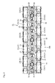
- the cell module 10 is configured to include, for example, a plurality (eleven, in Fig. 1 ) of the single cells 11 (a bank of single cells) and the cell wiring module 20 connecting the plurality of single cells 11.
- the single cells 11 include terminals 12A to 12C projecting perpendicularly from a top surface of a flat, rectangular main body, the main body housing a power generating element (not shown in the drawings) on an interior thereof.
- the terminals 12A to 12C are configured by a front-back pair of electrode terminals 12A and 12B (in the drawings, 12A is a positive electrode and 12B is a negative electrode), and a squared tubular terminal for voltage detection 12C provided at a portion intermediate to the pair of electrode terminals 12A and 12B.
- the terminal for voltage detection 12C detects a voltage of substantially a center of the electrode terminals 12A and 12B.
- Each of the electrode terminals 12A to 12C is a squared tubular nut (square nut) with a circular screw hole running through a center thereof.
- a shaft of a bolt is threaded with the electrode terminals 12A to 12C to fixate each of the connection members 21 and a voltage detection terminal 24.
- Each of the single cells 11 is arranged in an orientation such that polarities of adjacent electrode terminals 12A and 12B are opposite.
- the bank of single cells is fixated by a holding plate not shown in the drawings.
- the cell wiring module 20 is configured with a plurality of the connection members 21 connecting the electrode terminals 12A and 12B of the adjacent single cells 11; a plurality of the voltage detection terminals 24 detecting the voltage of the single cells 11; and a linked connection unit 20A made of a synthetic resin and housing the plurality of connection members 21 and the plurality of voltage detection terminals 24.
- connection member 21 is configured with a metal such as copper, a copper alloy, stainless steel (SUS), or aluminum. As shown in Fig. 3 , the connection member 21 has a plate shape of a length corresponding to a measurement between the adjacent electrode terminals 12A and 12B. In addition, a pair of through-holes 22 are formed running through the connection member 21, the shaft of the bolt being inserted through the through-holes 22 (communicating with the screw holes of the electrode terminals 12A and 12B). A shape of the through-holes 22 is an elliptical shape long in a left-right direction (a connection direction).
- a lateral edge in the connection direction of the connection member 21 has engaged recesses 23 formed at four locations on two sides of the through-holes 22, the engaged recesses 23 being formed by cutting a rectangular shape (step shape) with length in the front-back direction out of the lateral edge (formed by narrowing a width dimension of the connection member 21 in the step shape). Moreover, corners where the engaged recesses 23 constrict in the step shape have a slightly tapered shape.
- connection member 21 is configured with a linking connection member 21A linking a first unit 26 and a second unit 43, and with a housed connection member 21B housed entirely on the first unit 26 and the second unit 43.
- the connection members 21A and 21B have identical shapes.
- the engaged recess 23 provided on the linking connection member 21A of the connection members 21 is an example of an "engaged portion" configuring the present invention.
- the voltage detection terminal 24 includes a crimped portion where a voltage detection wire (not shown in the drawings) is crimped on a rear side of a rectangular flat plate portion.
- a circular through-hole 25 is formed in a center portion of the flat plate portion, through which the shaft of the bolt can be inserted.
- an exposed core wire portion on the end of the voltage detection wire is crimped.
- the voltage detection terminal 24 is positioned so as to line up with one side of each of the connection members 21, in addition to a detection housing.
- a recess is formed on a periphery of the connection members 21, the voltage detection terminal 24 fitting into the recess.
- the voltage detection wire is run through a wire through-trench 41 and connected to a cell ECU not shown in the drawings.
- a microcomputer, an element, and the like is installed in the cell ECU, which has a known configuration that includes functions for detection of the voltage, current, temperature, and the like of the single cells 11, and for performing control of power storage and release of each of the single cells 11, and the like.
- the linked connection unit 20A is configured to link, via the connection member 21, the first unit 26 and the second unit 43, the first unit 26 being provided on a first left-right direction side and housing the plurality of connection members 21 and the voltage detection terminals 24, the second unit 43 being provided on a second left-right direction side and housing the plurality of connection members 21 and the voltage detection terminals 24.
- the first unit 26 is made of a synthetic resin.
- the first unit 26 has a shape in which a front end protrudes in a step shape (crank shape) further to the right than a back end, and in which the back end protrudes in a step shape (crank shape) further to the left than the front end.
- the first unit 26 includes a housing 27, a holder 31, a detection housing 38, and the wire through-trench 41.
- the housing 27 is provided to each of a front and back of the first unit 26 and houses the housed connection member 21B.
- the holder 31 is provided to left and right ends aligned with the housing 27 and holds a first side in a length direction (connection direction) of the linking connection member 21A.
- the detection housing 38 is provided aligned with a front-back direction center portion and houses the voltage detection terminal 24.
- the voltage detection wire is passed through the wire through-trench 41.
- the housing portion 27 includes a base plate 28 on which the housed connection member 21B is placed, and a dividing wall 29 having a squared tube shape surrounding the housed connection member 21B.
- the base plate 28 links base ends of opposing dividing walls 29 at a left-right direction center portion of the dividing walls 29.
- Rectangular openings are formed to the left and right of the base plate 28.
- the openings are portions into which the electrode terminals 12A and 12B advance, and are slightly larger than the electrode terminals 12A and 12B.
- the dividing wall 29 is set to a height capable of preventing a short circuit caused by a tool or the like contacting the short connection member 21 or a top portion of the bolt.
- a pair of holding pieces 30 are provided at a left-right direction middle portion of the dividing wall 29, the holding pieces 30 holding the housed connection member 21B within the housing 27.
- the holding pieces 30 engage the connection member 21 on top of the base plate 28 by positioning a hook-shaped forefront end above front and back edges of the base plate 28.
- Each of the holding pieces 30 is formed by cutting a squared "U"-shaped notch from the dividing wall 29.
- a support wall is integrally formed with the dividing wall 29, the support wall covering the notched portions.
- the detection housing 38 includes a recess 39, into which the voltage detection terminal 24 is fitted and through which the voltage detection wire is passed, and a rectangular opening 40, through which the terminal for voltage detection 12C is passed.
- a positioner projecting in a squared frame shape is provided around the opening 40 on a reverse side of the detection housing 38. A top end portion of the terminal for voltage detection 12C of the single cell 11 is fitted into the positioner, thus positioning the first unit 26 with respect to the single cell 11 (a reference position of the first unit 26 with respect to the single cell 11 is fixed).
- Fitting projections 45 and 46 projecting to the left (connection direction) are provided on a left end of the four (plurality of) aligned detection housings 38 (a first end portion in the connection direction of the connection member 21 of the first unit 26 and between the front and back linking connection members 21A).
- fitting recesses 47 and 48 fitting together with the fitting projections 45 and 46 are provided on a right end of the four (plurality of) aligned detection housings 38 (a second end portion in the connection direction of the connection member 21 of the first unit 26 and between the front and back linking connection members 21A).
- the fitting projections 45 and 46 are both pole-shaped members and have a flat shape that is thick-walled in the vertical direction and thin-walled in the front-back direction.
- the fitting recesses 47 and 48 are formed with a depth and size capable of fitting together with the fitting projections 45 and 46 by inserting the fitting projections 45 and 46 until forefront ends thereof are halted.
- the base plate 32 is formed on left and right end portions of the first unit 26.
- a base plate 32A on a first left-right direction end has a shape in which both lateral edges rise up slightly, while a base plate 32B is formed on a second left-right direction end.
- the base plate 32A of the first unit 26 is fitted together with the base plate 32B of the second unit 43 and the base plate 32B of the first unit 26 is fitted together with the base plate 32A of the second unit 43.
- the base plate 32A receives the base plate 32B from below.
- a forefront end of the base plate 32B is capable of striking a portion formed on the base plate 32A side, the portion having a diameter constricted in a step shape.
- a portion with no base plate 32 forms a rectangular opening into which the cylindrical electrode terminals 12A and 12B can advance.
- the dividing wall 34 is set to a height capable of preventing a short circuit caused by a tool or the like contacting the connection member 21, the bolt, or the like.
- the dividing wall 34 is configured with a pair of opposing walls opposing on front and back, and a side wall connecting the pair of opposing walls. A side opposite the side wall is left open.
- a holding piece 36 is formed on each of the opposing walls for holding the linking connection member 21A within the holders 31 (on the base plate 28 side).
- the dividing wall 34 includes the squared "U"-shaped notch, thereby forming the holding piece 36 on an inner side of the notch.
- the holding piece 36 has a shape in which a projection dimension increases in a sloped shape (hook shape) toward the base plate 32 and, by positioning the forefront end side of the hook of the holding piece 36 above an edge portion of the linking connection member 21A, the linking connection member 21A is engaged between the bottom end of the holding piece 30 and the base plate 28.
- the engagement projection 37 projects toward an interior in a rectangular shape (a step shape) on a base end portion of each of the opposing walls in a position corresponding to the engaged recess 23 of the linking connection member 21A, i.e., in a position where the opening is formed through which the electrode terminals 12A and 12B are inserted.
- the projection dimension of the engagement projection 37 is slightly smaller than a notched depth dimension of the engaged recess 23 in a lateral surface of the connection member 21.
- the vertical-direction position of the engagement projection 37 is the same as that of the engaged recess 23 of the connection member 21. Corners of the engagement projection 37 have a tapered shape.
- a length of the engagement projection 37 in the left-right direction is smaller than a length of the engaged recess 23 in the left-right direction.
- a dimension of the engaged recess 23 is a dimension in which predetermined clearances CL1 and CL2 have been added to a front and back of the engagement projection 37.
- the second unit 43 has a shape identical to that of the first unit 26 and thus, as shown in Fig. 4 , identical reference numerals to those of the first unit 26 are given to the second unit 43 and descriptions thereof are omitted.
- the linking connection member 21A becomes slidable (slide displaceable) with respect to the second unit 43 in the left-right direction in a range of the predetermined clearances CL1 and CL2 (CL1 + CL2).
- the linking connection member 21A also becomes slidable (slide displaceable) with respect to the first unit 26 in the left-right direction in the range of the predetermined clearances CL1 and CL2 (CL1 + CL2).
- the cell wiring module 20 is formed in which the housed connection members 21B are housed in each of the housings 27 with respect to the first unit 26 and the second unit 43, the linking connection members 21A are held by each of the holders 31, and the voltage detection terminals 24 are mounted, the voltage detection wire being crimped in the voltage detection terminal 24 (see Fig. 2 ).
- the cell wiring module 20 is mounted such that the positioners provided to the reverse side of each of the units 26 and 43 are positioned by each of the terminals for voltage detection 12C of the plurality of single cells 11 positions.
- the first unit 26 and the second unit 43 can be slid left and right relative to each other by an amount corresponding to the clearance generated by the engagement projection 37 and the engaged recess 23.
- the shaft of the bolt is passed through the through-holes 22 of each of the connection members 21 and the connection members 21 are bolt-fastened between the electrode terminals 12A and 12B.
- the through-holes 22 have elliptical shapes long in the left-right direction, errors in the dimensional accuracy between the electrode terminals 12A and 12B can be absorbed by the elliptical through-holes 22 and the bolt-fastening can be performed more securely.
- Embodiment 2 is described with reference to Figs. 6 to 11 .
- the description is given with upward in Fig. 6 treated as forward and downward treated as rearward for the front-back direction, while a near face of a sheet of Fig. 6 is treated as upward and a far face of the sheet is treated as downward for the vertical direction.
- configurations identical to those of Embodiment 1 are given identical reference numerals and descriptions thereof are omitted.
- a cell module 50 is configured to include, for example, ten (a plurality) of the single cells 11 and a cell wiring module 51 connecting the ten single cells 11.
- the ten single cells 11 are divided into three rows in a long axis (long side) direction of the top surface of the single cells 11 (a surface having the electrode terminals). Two rows on a left side are stacked in four layers in a short axis direction of the top surface of the single cells 11, and one row on a right end is stacked in two layers in the short axis (short side) direction.
- the cell wiring module 51 is configured to include a plurality of the connection members 21 (short connection members) connecting the electrode terminals 12A and 12B on the top surfaces of different single cells 11 adjacent in the short axis direction; a plurality of the long connection members 52 connecting the electrode terminals 12A and 12B of different single cells 11 adjacent in the long axis direction; the voltage detection terminal 24 connected to the voltage detection wire; two (a plurality of) first units 56A and 56B housing the connection members 21 and holding the long connection member 52; three (a plurality of) second units 65A and 65B coupled to the first unit via the connection members 21 and 52; and a connection unit 70 connected to the second units 65A and 65B.
- connection members 21 short connection members
- the long connection members 52 connecting the electrode terminals 12A and 12B of different single cells 11 adjacent in the long axis direction
- the voltage detection terminal 24 connected to the voltage detection wire
- two (a plurality of) first units 56A and 56B housing the connection members 21 and holding the long connection member 52
- Engaged recesses 54 are formed on lateral edges on two sides of the through-holes 53 of the long connection member 52, the engaged recesses 54 being formed by cutting a rectangular shape (step shape) with length in the left-right direction out of the lateral edge (formed by narrowing a width dimension of the long connection member 52 in the step shape). Corners where the engaged recess 54 constricts in the step shape have a slightly tapered shape.
- the first units 56A and 56B are made of a synthetic resin and, as shown in Fig. 9 , are located on two sides of the second unit 65B. Both the first units 56A and 56B include the housing 27 housing the connection members 21; the detection housing 38 housing the voltage detection terminal 24; first holders 58A and 58B holding one side in the connection direction of the connection members 21 and 52; and a first positioner 63 ( Fig. 11 ) provided to the reverse face of the detection housing 38 and having the terminal for voltage detection 12C fitted and positioned therein.
- the housing 27 houses the entire connection member 21 within a single unit and, as shown in Fig. 9 , includes the base plate 28 on which the connection member 21 is placed, the dividing wall 29 having a squared tubular shape surrounding the connection member 21, and the pair of holding pieces 30 engaging the connection member 21 within the housing 27.
- the detection housing 38 includes the recess 39, into which the voltage detection terminal 24 is fitted and through which the voltage detection wire is passed, and the rectangular opening 40 through which the terminal for voltage detection 12C is passed. The voltage detection wire is led through one of the left and right grooves of the detection housing 38 toward the cell ECU.
- the first holders 58A and 58B are positioned such that the first holder 58A is provided so as to be capable of holding the connection member 21, the first holder 58B is provided so as to be capable of holding the long connection member 52, and the mounted connection members 21 and 52 are in a mutually orthogonal relationship.
- the first holders 58A and 58B both include a base plate 59 on which the connection members 21 and 52 are placed; a dividing wall 61 provided to a peripheral edge of the base plate 59 enclosing three sides and open on one side; a plurality of the holding pieces 36 projecting toward the inner surface of the dividing wall 61 and engaging on an upper surface side of the lateral edge of the connection members 21 and 52; and the engagement projection 37 allowing displacement (positioning drift) in the connection direction of the connection members 21 and 52 within a predetermined range (range of clearance) by engaging with the engaged recesses 23 and 54 of the connection members 21 and 52.
- a portion within the dividing walls 61 lacking the base plate 59 is an opening into which the top end portion of the electrode terminals 12A and 12B can advance.
- the dividing wall 61 is formed to a height capable of preventing a short circuit caused by a tool or the like contacting the electrode terminals 12A and 12B and the connection member 21.
- the dividing wall 61 is configured with a front-back pair of opposing walls and a side wall connecting the pair of opposing walls. A side opposite the side wall is left open.
- a plurality of the holding pieces 36 are provided to the opposing walls and a front-back pair of the holding pieces 36 project inward from a base end of each of the opposing walls.
- An engagement strength of each of the holding pieces 36 with respect to the connection members 21 and 52 (a strength of an engagement force determined chiefly by a dimension to the base plate 59) is set to a degree such that the connection members 21 and 52 do not escape from between the base plate 59 and the holding pieces 36 and such that the connection members 21 and 52 are capable of sliding in the connection direction.
- connection-direction ends of the engaged recess 54 have the clearances CL1 and CL2 (gaps) with the connection-direction ends of the engagement projection 37.
- connection members 21 and 52 are capable of sliding (capable of slide-displacing) in the front-back direction with respect to the first units 56A and 56B in the range of the predetermined clearances CL1 and CL2 (CL1 + CL2).
- an end portion connection member 55 is mounted on the first unit 56B and the connection unit 70, the end portion connection member 55 being connected to the electrode terminals 12A and 12B at an end of the connection (serial connection) of the single cells 11.
- a through-hole through which the shaft of the bolt is inserted is formed on the end portion connection member 55.
- an external connection terminal for connecting to a terminal of a wire linked to an external inverter or the like is provided projecting on the end portion connection member 55.
- the first positioner 63 is provided to the reverse face of the detection housing 38 so as to project in a squared frame shape (squared tube shape) encircling the opening 40.
- the first positioner 63 is positioned in a position of the terminal for voltage detection 12C by the squared tubular (rectangular) top end portion of the terminal for voltage detection 12C being accommodated (fitted) on an interior thereof with substantially no gaps.
- the second units 65A and 65B are made of a synthetic resin and, as shown in Fig. 9 , are provided at positions adjacent to the first units 56A and 56B.
- the second units 65A and 65B include the detection housing 38 housing the voltage detection terminal 24; a plurality of second holders 66A and 66B holding one side in the connection direction of the connection members 21 and 52; and a second positioner 67 ( Fig. 11 ) provided to the reverse face of the detection housing 38 and having the terminal for voltage detection 12C fitted and positioned therein.
- the dividing wall 61 is formed to a height capable of preventing a short circuit caused by a tool or the like contacting the electrode terminals 12A and 12B and the connection member 21.
- the dividing wall 61 is configured with the front-back pair of opposing walls and the side wall connecting the pair of opposing walls. The side opposite the side wall is left open.
- a plurality of the holding pieces 36 are provided to the opposing walls and a front-back pair of the holding pieces 36 project inward from the base end of each of the opposing walls.
- the engagement strength of each of the holding pieces 36 with respect to the connection members 21 and 52 (the strength of the engagement force determined chiefly by a dimension to the base plate 28) is set to a degree such that the long connection member 52 does not escape from between the base plate 28 and the holding pieces 36 and such that the connection members 21 and 52 are capable of sliding forward and backward.
- the second positioner 67 is provided to the reverse face of the detection housing 38 so as to project in a frame shape encircling an opening.
- the first positioner 63 is positioned in a position of the terminal for voltage detection 12C by the squared tubular (rectangular) top end portion of the terminal for voltage detection 12C being accommodated (fitted) on an interior thereof with substantially no gaps.
- the holder 71 is provided in a plurality of locations so as to be capable of holding the connection members 21 and 52.
- the holder 71 includes the base plate 59 on which the connection members 21 and 52 are placed; the dividing wall 61 provided to the peripheral edge of the base plate 59 enclosing three sides and open on one side; a plurality of the holding pieces 36 projecting toward the inner surface of the dividing wall 61 and engaging on the upper surface side of the lateral edge of the connection members 21 and 52; and the engagement projection 37 allowing displacement (positioning drift) in the connection direction of the connection members 21 and 52 within a predetermined range by engaging with the engaged recesses 23 and 54 of the connection members 21 and 52.
- the fitting projections 45 and 46 are both pole-shaped members and have a flat shape that is thick-walled in the vertical direction and thin-walled in the left-right direction.
- the fitting recesses 47 and 48 are formed with a depth and size capable of fitting together with the fitting projections 45 and 46 by inserting the fitting projections 45 and 46 until forefront ends thereof are halted.
- the base plate 59 on which the connection members 21 and 52 (used in connection) are placed is configured with a base plate 59A and a base plate 59B. Both lateral edges of the base plate 59A rise up slightly and end portions in the connection direction expand in a step shape.
- the base plate 59B is fitted into an interior of the base plate 59A.
- the base plate 59A receives the base plate 59B from below. Also, a forefront end of the base plate 59B is capable of striking the step portion of the base plate 59A.
- the cell wiring module 51 is formed in which the connection members 21 and 52 corresponding to each of the housings 27 and to each of the holders 58A, 58B, 66A, 66B, and 71 are mounted thereon ( Fig. 7 ) and, in addition, the voltage detection terminals 24 are mounted thereon, the voltage detection terminal 24 having the voltage detection wire crimped thereto.
- the cell wiring module 51 is integrally mounted to the plurality of single cells 11 such that each of the positioners 63 and 67 of each of the units 56A, 56B, 65A, 65B, and 70 are positioned on each of the terminals for voltage detection 12C of the plurality of single cells 11.
- each of the units 56A, 56B, 65A, 65B, and 70 can be slid up and down or left and right relative to each other by an amount corresponding to the clearances CL1 and CL2 of the engagement projections 37 and the engaged recesses 23 and 54.
- the shaft of the bolt is passed through the through-holes 22 and 53 of the connection members 21 and 52, respectively, and the bolt is fastened.
- the through-holes 22 and 53 have an elliptical shape long in the connection direction, and thus are able to absorb dimensional errors.
- Variation in dimensional accuracy is particularly likely to occur with regard to the long axis direction of the single cell 11 due to the length of the axis, and thus a dimensional error between the plurality of single cells 11 and the cell wiring module 20 is likely to increase.
- failure caused by a dimensional error can be prevented in such a case where dimensional errors are likely to occur.
- the plurality of single cells 11 are also aligned in the short axis direction of the surface having the electrode terminals 12A and 12B, and the connection member 21 connects the electrode terminals 12A and 12B aligned in the short axis direction. Therefore, a degree of freedom of connection of the plurality of single cells 11 can be increased.
Landscapes
- Chemical & Material Sciences (AREA)
- Chemical Kinetics & Catalysis (AREA)
- Electrochemistry (AREA)
- General Chemical & Material Sciences (AREA)
- Connection Of Batteries Or Terminals (AREA)
- Battery Mounting, Suspending (AREA)
Applications Claiming Priority (2)
| Application Number | Priority Date | Filing Date | Title |
|---|---|---|---|
| JP2011149075A JP5585846B2 (ja) | 2011-07-05 | 2011-07-05 | 電池配線モジュール |
| PCT/JP2012/064264 WO2013005515A1 (ja) | 2011-07-05 | 2012-06-01 | 電池配線モジュール |
Publications (3)
| Publication Number | Publication Date |
|---|---|
| EP2713422A1 true EP2713422A1 (de) | 2014-04-02 |
| EP2713422A4 EP2713422A4 (de) | 2014-12-31 |
| EP2713422B1 EP2713422B1 (de) | 2017-07-26 |
Family
ID=47436872
Family Applications (1)
| Application Number | Title | Priority Date | Filing Date |
|---|---|---|---|
| EP12807275.8A Active EP2713422B1 (de) | 2011-07-05 | 2012-06-01 | Zellenverkabelungsmodul |
Country Status (5)
| Country | Link |
|---|---|
| US (2) | US20140065468A1 (de) |
| EP (1) | EP2713422B1 (de) |
| JP (1) | JP5585846B2 (de) |
| CN (1) | CN103548180B (de) |
| WO (1) | WO2013005515A1 (de) |
Cited By (2)
| Publication number | Priority date | Publication date | Assignee | Title |
|---|---|---|---|---|
| EP2840629A4 (de) * | 2012-06-07 | 2015-05-27 | Autonetworks Technologies Ltd | Verkabelungsmodul |
| DE102016222703B4 (de) | 2015-11-20 | 2023-10-19 | Yazaki Corporation | Stromschienenhaltestruktur |
Families Citing this family (16)
| Publication number | Priority date | Publication date | Assignee | Title |
|---|---|---|---|---|
| WO2011052699A1 (ja) * | 2009-10-28 | 2011-05-05 | 矢崎総業株式会社 | バッテリ極柱接続用バスバーとこれを用いたバッテリ電圧監視装置 |
| JP5720448B2 (ja) * | 2011-07-11 | 2015-05-20 | 株式会社オートネットワーク技術研究所 | 電池配線モジュール |
| JP5811396B2 (ja) * | 2011-08-02 | 2015-11-11 | 株式会社オートネットワーク技術研究所 | 電池配線モジュール |
| JP6068059B2 (ja) | 2012-08-30 | 2017-01-25 | 矢崎総業株式会社 | バスバモジュール |
| JP6186922B2 (ja) * | 2013-06-18 | 2017-08-30 | 住友電装株式会社 | 配線モジュール |
| JP6098444B2 (ja) * | 2013-09-02 | 2017-03-22 | 株式会社デンソー | 組電池 |
| JP6198061B2 (ja) | 2013-10-28 | 2017-09-20 | 株式会社オートネットワーク技術研究所 | 配線モジュール |
| US20150214534A1 (en) * | 2014-01-27 | 2015-07-30 | Ford Global Technologies, Llc | Devices and methods for connecting battery cells |
| JP6256326B2 (ja) * | 2014-12-17 | 2018-01-10 | 株式会社オートネットワーク技術研究所 | 検知モジュール |
| JP6465354B2 (ja) * | 2015-05-28 | 2019-02-06 | 株式会社オートネットワーク技術研究所 | 蓄電モジュール |
| JP2017033646A (ja) * | 2015-07-29 | 2017-02-09 | 株式会社豊田自動織機 | 電池モジュールの製造方法 |
| JP6481860B2 (ja) * | 2015-08-07 | 2019-03-13 | 株式会社オートネットワーク技術研究所 | 支持部材 |
| JP6299917B1 (ja) | 2017-08-09 | 2018-03-28 | 株式会社オートネットワーク技術研究所 | 接続モジュール |
| JP7004197B2 (ja) * | 2017-09-22 | 2022-01-21 | 株式会社オートネットワーク技術研究所 | 電気接続部材 |
| JP6988687B2 (ja) * | 2018-05-21 | 2022-01-05 | 株式会社オートネットワーク技術研究所 | 配線モジュール |
| JP6981924B2 (ja) * | 2018-06-01 | 2021-12-17 | 株式会社オートネットワーク技術研究所 | 配線モジュール |
Citations (4)
| Publication number | Priority date | Publication date | Assignee | Title |
|---|---|---|---|---|
| EP0765005A2 (de) * | 1995-09-19 | 1997-03-26 | Sumitomo Wiring Systems, Ltd. | Elektrische Verbindungsanordnung mit Deckel sowie Deckel für eine elektrische Verbindungsanordnung |
| EP0986114A1 (de) * | 1998-09-09 | 2000-03-15 | Yazaki Corporation | Batterie-Verbindungsplatte |
| JP2011008955A (ja) * | 2009-06-23 | 2011-01-13 | Autonetworks Technologies Ltd | 電池接続アセンブリ |
| EP2685526A1 (de) * | 2011-03-07 | 2014-01-15 | AutoNetworks Technologies, Ltd. | Zellverbindungsanordnung |
Family Cites Families (10)
| Publication number | Priority date | Publication date | Assignee | Title |
|---|---|---|---|---|
| JP3409239B2 (ja) * | 1997-06-30 | 2003-05-26 | 住友電装株式会社 | バッテリーと電気接続箱との接続構造 |
| JPH1186831A (ja) * | 1997-09-04 | 1999-03-30 | Harness Sogo Gijutsu Kenkyusho:Kk | バッテリーの接続構造 |
| JP3811348B2 (ja) * | 2000-11-27 | 2006-08-16 | 矢崎総業株式会社 | バッテリ接続プレート |
| KR100627294B1 (ko) * | 2004-10-28 | 2006-09-25 | 삼성에스디아이 주식회사 | 전지 모듈 |
| JP5127154B2 (ja) * | 2005-05-23 | 2013-01-23 | パナソニック株式会社 | 電池モジュール |
| JP5139745B2 (ja) * | 2007-08-10 | 2013-02-06 | 矢崎総業株式会社 | 電源装置 |
| JP5141965B2 (ja) * | 2008-04-09 | 2013-02-13 | 株式会社デンソー | 組電池 |
| JP5537111B2 (ja) * | 2009-09-30 | 2014-07-02 | 株式会社東芝 | 二次電池装置 |
| US8460818B2 (en) * | 2009-10-05 | 2013-06-11 | Samsung Sdi Co., Ltd. | Battery module |
| KR101146677B1 (ko) * | 2009-10-30 | 2012-05-22 | 에스비리모티브 주식회사 | 버스바홀더 |
-
2011
- 2011-07-05 JP JP2011149075A patent/JP5585846B2/ja not_active Expired - Fee Related
-
2012
- 2012-06-01 CN CN201280024547.4A patent/CN103548180B/zh active Active
- 2012-06-01 WO PCT/JP2012/064264 patent/WO2013005515A1/ja active Application Filing
- 2012-06-01 EP EP12807275.8A patent/EP2713422B1/de active Active
- 2012-06-01 US US14/114,807 patent/US20140065468A1/en not_active Abandoned
-
2016
- 2016-07-11 US US15/206,716 patent/US10020484B2/en active Active
Patent Citations (4)
| Publication number | Priority date | Publication date | Assignee | Title |
|---|---|---|---|---|
| EP0765005A2 (de) * | 1995-09-19 | 1997-03-26 | Sumitomo Wiring Systems, Ltd. | Elektrische Verbindungsanordnung mit Deckel sowie Deckel für eine elektrische Verbindungsanordnung |
| EP0986114A1 (de) * | 1998-09-09 | 2000-03-15 | Yazaki Corporation | Batterie-Verbindungsplatte |
| JP2011008955A (ja) * | 2009-06-23 | 2011-01-13 | Autonetworks Technologies Ltd | 電池接続アセンブリ |
| EP2685526A1 (de) * | 2011-03-07 | 2014-01-15 | AutoNetworks Technologies, Ltd. | Zellverbindungsanordnung |
Non-Patent Citations (1)
| Title |
|---|
| See also references of WO2013005515A1 * |
Cited By (3)
| Publication number | Priority date | Publication date | Assignee | Title |
|---|---|---|---|---|
| EP2840629A4 (de) * | 2012-06-07 | 2015-05-27 | Autonetworks Technologies Ltd | Verkabelungsmodul |
| US9991495B2 (en) | 2012-06-07 | 2018-06-05 | Sumitomo Wiring Systems, Ltd. | Wiring module |
| DE102016222703B4 (de) | 2015-11-20 | 2023-10-19 | Yazaki Corporation | Stromschienenhaltestruktur |
Also Published As
| Publication number | Publication date |
|---|---|
| US10020484B2 (en) | 2018-07-10 |
| CN103548180A (zh) | 2014-01-29 |
| EP2713422A4 (de) | 2014-12-31 |
| JP5585846B2 (ja) | 2014-09-10 |
| EP2713422B1 (de) | 2017-07-26 |
| WO2013005515A1 (ja) | 2013-01-10 |
| CN103548180B (zh) | 2016-03-09 |
| US20160322625A1 (en) | 2016-11-03 |
| JP2013016380A (ja) | 2013-01-24 |
| US20140065468A1 (en) | 2014-03-06 |
Similar Documents
| Publication | Publication Date | Title |
|---|---|---|
| US10020484B2 (en) | Cell wiring module | |
| US9997757B2 (en) | Cell connection assembly | |
| JP6164489B2 (ja) | 配線モジュール | |
| US9184432B2 (en) | Cell wiring module | |
| US9905831B2 (en) | Cell wiring module | |
| WO2013084713A1 (ja) | 電池配線モジュール | |
| JP6176126B2 (ja) | 配線モジュールおよび蓄電モジュール | |
| JP5209766B2 (ja) | 電池配線モジュールのカバー、及び電池配線モジュール | |
| US9660243B2 (en) | Battery wiring module | |
| CN103891007A (zh) | 电池模块以及配线模块 | |
| EP2840629A1 (de) | Verkabelungsmodul | |
| EP3457463A1 (de) | Anschlussmodul | |
| JP2013054997A (ja) | 電池配線モジュール | |
| JP5757180B2 (ja) | 電池配線モジュールのカバー、電池配線モジュール及び電池モジュール | |
| JP5672188B2 (ja) | 電池配線モジュール | |
| JP5790742B2 (ja) | 電池接続アセンブリ |
Legal Events
| Date | Code | Title | Description |
|---|---|---|---|
| PUAI | Public reference made under article 153(3) epc to a published international application that has entered the european phase |
Free format text: ORIGINAL CODE: 0009012 |
|
| 17P | Request for examination filed |
Effective date: 20131227 |
|
| AK | Designated contracting states |
Kind code of ref document: A1 Designated state(s): AL AT BE BG CH CY CZ DE DK EE ES FI FR GB GR HR HU IE IS IT LI LT LU LV MC MK MT NL NO PL PT RO RS SE SI SK SM TR |
|
| RIN1 | Information on inventor provided before grant (corrected) |
Inventor name: NAKAYAMA, OSAMU |
|
| DAX | Request for extension of the european patent (deleted) | ||
| A4 | Supplementary search report drawn up and despatched |
Effective date: 20141202 |
|
| RIC1 | Information provided on ipc code assigned before grant |
Ipc: H01M 2/20 20060101AFI20141126BHEP |
|
| GRAJ | Information related to disapproval of communication of intention to grant by the applicant or resumption of examination proceedings by the epo deleted |
Free format text: ORIGINAL CODE: EPIDOSDIGR1 |
|
| STAA | Information on the status of an ep patent application or granted ep patent |
Free format text: STATUS: GRANT OF PATENT IS INTENDED |
|
| GRAP | Despatch of communication of intention to grant a patent |
Free format text: ORIGINAL CODE: EPIDOSNIGR1 |
|
| INTG | Intention to grant announced |
Effective date: 20170314 |
|
| RIN1 | Information on inventor provided before grant (corrected) |
Inventor name: NAKAYAMA, OSAMU |
|
| GRAS | Grant fee paid |
Free format text: ORIGINAL CODE: EPIDOSNIGR3 |
|
| GRAA | (expected) grant |
Free format text: ORIGINAL CODE: 0009210 |
|
| STAA | Information on the status of an ep patent application or granted ep patent |
Free format text: STATUS: THE PATENT HAS BEEN GRANTED |
|
| AK | Designated contracting states |
Kind code of ref document: B1 Designated state(s): AL AT BE BG CH CY CZ DE DK EE ES FI FR GB GR HR HU IE IS IT LI LT LU LV MC MK MT NL NO PL PT RO RS SE SI SK SM TR |
|
| REG | Reference to a national code |
Ref country code: GB Ref legal event code: FG4D Ref country code: DE Ref legal event code: R082 Ref document number: 602012035086 Country of ref document: DE Representative=s name: HORN KLEIMANN WAITZHOFER PATENTANWAELTE PARTG , DE |
|
| REG | Reference to a national code |
Ref country code: CH Ref legal event code: EP |
|
| REG | Reference to a national code |
Ref country code: AT Ref legal event code: REF Ref document number: 913073 Country of ref document: AT Kind code of ref document: T Effective date: 20170815 |
|
| REG | Reference to a national code |
Ref country code: IE Ref legal event code: FG4D |
|
| REG | Reference to a national code |
Ref country code: DE Ref legal event code: R096 Ref document number: 602012035086 Country of ref document: DE |
|
| REG | Reference to a national code |
Ref country code: NL Ref legal event code: MP Effective date: 20170726 |
|
| REG | Reference to a national code |
Ref country code: LT Ref legal event code: MG4D |
|
| REG | Reference to a national code |
Ref country code: AT Ref legal event code: MK05 Ref document number: 913073 Country of ref document: AT Kind code of ref document: T Effective date: 20170726 |
|
| PG25 | Lapsed in a contracting state [announced via postgrant information from national office to epo] |
Ref country code: SE Free format text: LAPSE BECAUSE OF FAILURE TO SUBMIT A TRANSLATION OF THE DESCRIPTION OR TO PAY THE FEE WITHIN THE PRESCRIBED TIME-LIMIT Effective date: 20170726 Ref country code: NL Free format text: LAPSE BECAUSE OF FAILURE TO SUBMIT A TRANSLATION OF THE DESCRIPTION OR TO PAY THE FEE WITHIN THE PRESCRIBED TIME-LIMIT Effective date: 20170726 Ref country code: LT Free format text: LAPSE BECAUSE OF FAILURE TO SUBMIT A TRANSLATION OF THE DESCRIPTION OR TO PAY THE FEE WITHIN THE PRESCRIBED TIME-LIMIT Effective date: 20170726 Ref country code: FI Free format text: LAPSE BECAUSE OF FAILURE TO SUBMIT A TRANSLATION OF THE DESCRIPTION OR TO PAY THE FEE WITHIN THE PRESCRIBED TIME-LIMIT Effective date: 20170726 Ref country code: HR Free format text: LAPSE BECAUSE OF FAILURE TO SUBMIT A TRANSLATION OF THE DESCRIPTION OR TO PAY THE FEE WITHIN THE PRESCRIBED TIME-LIMIT Effective date: 20170726 Ref country code: NO Free format text: LAPSE BECAUSE OF FAILURE TO SUBMIT A TRANSLATION OF THE DESCRIPTION OR TO PAY THE FEE WITHIN THE PRESCRIBED TIME-LIMIT Effective date: 20171026 Ref country code: AT Free format text: LAPSE BECAUSE OF FAILURE TO SUBMIT A TRANSLATION OF THE DESCRIPTION OR TO PAY THE FEE WITHIN THE PRESCRIBED TIME-LIMIT Effective date: 20170726 |
|
| PG25 | Lapsed in a contracting state [announced via postgrant information from national office to epo] |
Ref country code: PL Free format text: LAPSE BECAUSE OF FAILURE TO SUBMIT A TRANSLATION OF THE DESCRIPTION OR TO PAY THE FEE WITHIN THE PRESCRIBED TIME-LIMIT Effective date: 20170726 Ref country code: ES Free format text: LAPSE BECAUSE OF FAILURE TO SUBMIT A TRANSLATION OF THE DESCRIPTION OR TO PAY THE FEE WITHIN THE PRESCRIBED TIME-LIMIT Effective date: 20170726 Ref country code: IS Free format text: LAPSE BECAUSE OF FAILURE TO SUBMIT A TRANSLATION OF THE DESCRIPTION OR TO PAY THE FEE WITHIN THE PRESCRIBED TIME-LIMIT Effective date: 20171126 Ref country code: LV Free format text: LAPSE BECAUSE OF FAILURE TO SUBMIT A TRANSLATION OF THE DESCRIPTION OR TO PAY THE FEE WITHIN THE PRESCRIBED TIME-LIMIT Effective date: 20170726 Ref country code: RS Free format text: LAPSE BECAUSE OF FAILURE TO SUBMIT A TRANSLATION OF THE DESCRIPTION OR TO PAY THE FEE WITHIN THE PRESCRIBED TIME-LIMIT Effective date: 20170726 Ref country code: BG Free format text: LAPSE BECAUSE OF FAILURE TO SUBMIT A TRANSLATION OF THE DESCRIPTION OR TO PAY THE FEE WITHIN THE PRESCRIBED TIME-LIMIT Effective date: 20171026 Ref country code: GR Free format text: LAPSE BECAUSE OF FAILURE TO SUBMIT A TRANSLATION OF THE DESCRIPTION OR TO PAY THE FEE WITHIN THE PRESCRIBED TIME-LIMIT Effective date: 20171027 |
|
| PG25 | Lapsed in a contracting state [announced via postgrant information from national office to epo] |
Ref country code: DK Free format text: LAPSE BECAUSE OF FAILURE TO SUBMIT A TRANSLATION OF THE DESCRIPTION OR TO PAY THE FEE WITHIN THE PRESCRIBED TIME-LIMIT Effective date: 20170726 Ref country code: CZ Free format text: LAPSE BECAUSE OF FAILURE TO SUBMIT A TRANSLATION OF THE DESCRIPTION OR TO PAY THE FEE WITHIN THE PRESCRIBED TIME-LIMIT Effective date: 20170726 Ref country code: RO Free format text: LAPSE BECAUSE OF FAILURE TO SUBMIT A TRANSLATION OF THE DESCRIPTION OR TO PAY THE FEE WITHIN THE PRESCRIBED TIME-LIMIT Effective date: 20170726 |
|
| REG | Reference to a national code |
Ref country code: DE Ref legal event code: R097 Ref document number: 602012035086 Country of ref document: DE |
|
| PG25 | Lapsed in a contracting state [announced via postgrant information from national office to epo] |
Ref country code: SK Free format text: LAPSE BECAUSE OF FAILURE TO SUBMIT A TRANSLATION OF THE DESCRIPTION OR TO PAY THE FEE WITHIN THE PRESCRIBED TIME-LIMIT Effective date: 20170726 Ref country code: EE Free format text: LAPSE BECAUSE OF FAILURE TO SUBMIT A TRANSLATION OF THE DESCRIPTION OR TO PAY THE FEE WITHIN THE PRESCRIBED TIME-LIMIT Effective date: 20170726 Ref country code: SM Free format text: LAPSE BECAUSE OF FAILURE TO SUBMIT A TRANSLATION OF THE DESCRIPTION OR TO PAY THE FEE WITHIN THE PRESCRIBED TIME-LIMIT Effective date: 20170726 Ref country code: IT Free format text: LAPSE BECAUSE OF FAILURE TO SUBMIT A TRANSLATION OF THE DESCRIPTION OR TO PAY THE FEE WITHIN THE PRESCRIBED TIME-LIMIT Effective date: 20170726 |
|
| PLBE | No opposition filed within time limit |
Free format text: ORIGINAL CODE: 0009261 |
|
| STAA | Information on the status of an ep patent application or granted ep patent |
Free format text: STATUS: NO OPPOSITION FILED WITHIN TIME LIMIT |
|
| 26N | No opposition filed |
Effective date: 20180430 |
|
| PG25 | Lapsed in a contracting state [announced via postgrant information from national office to epo] |
Ref country code: SI Free format text: LAPSE BECAUSE OF FAILURE TO SUBMIT A TRANSLATION OF THE DESCRIPTION OR TO PAY THE FEE WITHIN THE PRESCRIBED TIME-LIMIT Effective date: 20170726 |
|
| REG | Reference to a national code |
Ref country code: CH Ref legal event code: PL |
|
| GBPC | Gb: european patent ceased through non-payment of renewal fee |
Effective date: 20180601 |
|
| REG | Reference to a national code |
Ref country code: BE Ref legal event code: MM Effective date: 20180630 |
|
| REG | Reference to a national code |
Ref country code: IE Ref legal event code: MM4A |
|
| PG25 | Lapsed in a contracting state [announced via postgrant information from national office to epo] |
Ref country code: LU Free format text: LAPSE BECAUSE OF NON-PAYMENT OF DUE FEES Effective date: 20180601 Ref country code: MC Free format text: LAPSE BECAUSE OF FAILURE TO SUBMIT A TRANSLATION OF THE DESCRIPTION OR TO PAY THE FEE WITHIN THE PRESCRIBED TIME-LIMIT Effective date: 20170726 |
|
| PG25 | Lapsed in a contracting state [announced via postgrant information from national office to epo] |
Ref country code: GB Free format text: LAPSE BECAUSE OF NON-PAYMENT OF DUE FEES Effective date: 20180601 Ref country code: FR Free format text: LAPSE BECAUSE OF NON-PAYMENT OF DUE FEES Effective date: 20180630 Ref country code: CH Free format text: LAPSE BECAUSE OF NON-PAYMENT OF DUE FEES Effective date: 20180630 Ref country code: LI Free format text: LAPSE BECAUSE OF NON-PAYMENT OF DUE FEES Effective date: 20180630 Ref country code: IE Free format text: LAPSE BECAUSE OF NON-PAYMENT OF DUE FEES Effective date: 20180601 |
|
| PG25 | Lapsed in a contracting state [announced via postgrant information from national office to epo] |
Ref country code: BE Free format text: LAPSE BECAUSE OF NON-PAYMENT OF DUE FEES Effective date: 20180630 |
|
| PG25 | Lapsed in a contracting state [announced via postgrant information from national office to epo] |
Ref country code: MT Free format text: LAPSE BECAUSE OF NON-PAYMENT OF DUE FEES Effective date: 20180601 |
|
| PG25 | Lapsed in a contracting state [announced via postgrant information from national office to epo] |
Ref country code: TR Free format text: LAPSE BECAUSE OF FAILURE TO SUBMIT A TRANSLATION OF THE DESCRIPTION OR TO PAY THE FEE WITHIN THE PRESCRIBED TIME-LIMIT Effective date: 20170726 |
|
| PG25 | Lapsed in a contracting state [announced via postgrant information from national office to epo] |
Ref country code: HU Free format text: LAPSE BECAUSE OF FAILURE TO SUBMIT A TRANSLATION OF THE DESCRIPTION OR TO PAY THE FEE WITHIN THE PRESCRIBED TIME-LIMIT; INVALID AB INITIO Effective date: 20120601 Ref country code: PT Free format text: LAPSE BECAUSE OF FAILURE TO SUBMIT A TRANSLATION OF THE DESCRIPTION OR TO PAY THE FEE WITHIN THE PRESCRIBED TIME-LIMIT Effective date: 20170726 |
|
| PG25 | Lapsed in a contracting state [announced via postgrant information from national office to epo] |
Ref country code: MK Free format text: LAPSE BECAUSE OF NON-PAYMENT OF DUE FEES Effective date: 20170726 Ref country code: CY Free format text: LAPSE BECAUSE OF FAILURE TO SUBMIT A TRANSLATION OF THE DESCRIPTION OR TO PAY THE FEE WITHIN THE PRESCRIBED TIME-LIMIT Effective date: 20170726 |
|
| PG25 | Lapsed in a contracting state [announced via postgrant information from national office to epo] |
Ref country code: AL Free format text: LAPSE BECAUSE OF FAILURE TO SUBMIT A TRANSLATION OF THE DESCRIPTION OR TO PAY THE FEE WITHIN THE PRESCRIBED TIME-LIMIT Effective date: 20170726 |
|
| REG | Reference to a national code |
Ref country code: DE Ref legal event code: R079 Ref document number: 602012035086 Country of ref document: DE Free format text: PREVIOUS MAIN CLASS: H01M0002200000 Ipc: H01M0050500000 |
|
| REG | Reference to a national code |
Ref country code: DE Ref legal event code: R084 Ref document number: 602012035086 Country of ref document: DE |
|
| P01 | Opt-out of the competence of the unified patent court (upc) registered |
Effective date: 20230517 |
|
| PGFP | Annual fee paid to national office [announced via postgrant information from national office to epo] |
Ref country code: DE Payment date: 20230502 Year of fee payment: 12 |