EP2710733B1 - Charge-sensitive amplifier - Google Patents
Charge-sensitive amplifier Download PDFInfo
- Publication number
- EP2710733B1 EP2710733B1 EP12725134.6A EP12725134A EP2710733B1 EP 2710733 B1 EP2710733 B1 EP 2710733B1 EP 12725134 A EP12725134 A EP 12725134A EP 2710733 B1 EP2710733 B1 EP 2710733B1
- Authority
- EP
- European Patent Office
- Prior art keywords
- charge
- gate
- bond pad
- sensitive amplifier
- capacitor
- Prior art date
- Legal status (The legal status is an assumption and is not a legal conclusion. Google has not performed a legal analysis and makes no representation as to the accuracy of the status listed.)
- Active
Links
- 239000003990 capacitor Substances 0.000 claims description 47
- 239000000758 substrate Substances 0.000 claims description 27
- 239000004065 semiconductor Substances 0.000 claims description 25
- 230000005669 field effect Effects 0.000 claims description 24
- 239000000463 material Substances 0.000 claims description 21
- 239000002245 particle Substances 0.000 claims description 21
- 229910052710 silicon Inorganic materials 0.000 claims description 16
- 239000010703 silicon Substances 0.000 claims description 16
- XUIMIQQOPSSXEZ-UHFFFAOYSA-N Silicon Chemical group [Si] XUIMIQQOPSSXEZ-UHFFFAOYSA-N 0.000 claims description 13
- 230000003071 parasitic effect Effects 0.000 claims description 9
- 230000003321 amplification Effects 0.000 claims description 6
- 238000003199 nucleic acid amplification method Methods 0.000 claims description 6
- 238000000926 separation method Methods 0.000 claims description 2
- 230000005855 radiation Effects 0.000 description 10
- 238000001514 detection method Methods 0.000 description 8
- 239000010410 layer Substances 0.000 description 7
- 229910052751 metal Inorganic materials 0.000 description 7
- 239000002184 metal Substances 0.000 description 7
- 239000004411 aluminium Substances 0.000 description 6
- 229910052782 aluminium Inorganic materials 0.000 description 6
- XAGFODPZIPBFFR-UHFFFAOYSA-N aluminium Chemical compound [Al] XAGFODPZIPBFFR-UHFFFAOYSA-N 0.000 description 6
- 238000000034 method Methods 0.000 description 6
- 230000008901 benefit Effects 0.000 description 5
- VYPSYNLAJGMNEJ-UHFFFAOYSA-N Silicium dioxide Chemical compound O=[Si]=O VYPSYNLAJGMNEJ-UHFFFAOYSA-N 0.000 description 4
- 238000013461 design Methods 0.000 description 3
- 238000004519 manufacturing process Methods 0.000 description 3
- 230000008569 process Effects 0.000 description 3
- 238000009413 insulation Methods 0.000 description 2
- 230000009467 reduction Effects 0.000 description 2
- 230000035945 sensitivity Effects 0.000 description 2
- 239000000377 silicon dioxide Substances 0.000 description 2
- 235000012239 silicon dioxide Nutrition 0.000 description 2
- 239000002210 silicon-based material Substances 0.000 description 2
- 238000013459 approach Methods 0.000 description 1
- 238000000151 deposition Methods 0.000 description 1
- 238000011161 development Methods 0.000 description 1
- 230000000694 effects Effects 0.000 description 1
- 238000003384 imaging method Methods 0.000 description 1
- 230000006872 improvement Effects 0.000 description 1
- 230000010354 integration Effects 0.000 description 1
- 150000002500 ions Chemical class 0.000 description 1
- 238000002955 isolation Methods 0.000 description 1
- 238000001459 lithography Methods 0.000 description 1
- 238000005259 measurement Methods 0.000 description 1
- 230000003287 optical effect Effects 0.000 description 1
- 238000011160 research Methods 0.000 description 1
- 239000002344 surface layer Substances 0.000 description 1
Images

Classifications
-
- H—ELECTRICITY
- H03—ELECTRONIC CIRCUITRY
- H03F—AMPLIFIERS
- H03F3/00—Amplifiers with only discharge tubes or only semiconductor devices as amplifying elements
- H03F3/70—Charge amplifiers
-
- G—PHYSICS
- G01—MEASURING; TESTING
- G01T—MEASUREMENT OF NUCLEAR OR X-RADIATION
- G01T1/00—Measuring X-radiation, gamma radiation, corpuscular radiation, or cosmic radiation
- G01T1/16—Measuring radiation intensity
- G01T1/17—Circuit arrangements not adapted to a particular type of detector
-
- G—PHYSICS
- G06—COMPUTING; CALCULATING OR COUNTING
- G06G—ANALOGUE COMPUTERS
- G06G7/00—Devices in which the computing operation is performed by varying electric or magnetic quantities
- G06G7/12—Arrangements for performing computing operations, e.g. operational amplifiers
- G06G7/18—Arrangements for performing computing operations, e.g. operational amplifiers for integration or differentiation; for forming integrals
- G06G7/184—Arrangements for performing computing operations, e.g. operational amplifiers for integration or differentiation; for forming integrals using capacitive elements
- G06G7/186—Arrangements for performing computing operations, e.g. operational amplifiers for integration or differentiation; for forming integrals using capacitive elements using an operational amplifier comprising a capacitor or a resistor in the feedback loop
-
- H—ELECTRICITY
- H01—ELECTRIC ELEMENTS
- H01L—SEMICONDUCTOR DEVICES NOT COVERED BY CLASS H10
- H01L27/00—Devices consisting of a plurality of semiconductor or other solid-state components formed in or on a common substrate
- H01L27/02—Devices consisting of a plurality of semiconductor or other solid-state components formed in or on a common substrate including semiconductor components specially adapted for rectifying, oscillating, amplifying or switching and having at least one potential-jump barrier or surface barrier; including integrated passive circuit elements with at least one potential-jump barrier or surface barrier
- H01L27/04—Devices consisting of a plurality of semiconductor or other solid-state components formed in or on a common substrate including semiconductor components specially adapted for rectifying, oscillating, amplifying or switching and having at least one potential-jump barrier or surface barrier; including integrated passive circuit elements with at least one potential-jump barrier or surface barrier the substrate being a semiconductor body
- H01L27/06—Devices consisting of a plurality of semiconductor or other solid-state components formed in or on a common substrate including semiconductor components specially adapted for rectifying, oscillating, amplifying or switching and having at least one potential-jump barrier or surface barrier; including integrated passive circuit elements with at least one potential-jump barrier or surface barrier the substrate being a semiconductor body including a plurality of individual components in a non-repetitive configuration
- H01L27/0611—Devices consisting of a plurality of semiconductor or other solid-state components formed in or on a common substrate including semiconductor components specially adapted for rectifying, oscillating, amplifying or switching and having at least one potential-jump barrier or surface barrier; including integrated passive circuit elements with at least one potential-jump barrier or surface barrier the substrate being a semiconductor body including a plurality of individual components in a non-repetitive configuration integrated circuits having a two-dimensional layout of components without a common active region
- H01L27/0617—Devices consisting of a plurality of semiconductor or other solid-state components formed in or on a common substrate including semiconductor components specially adapted for rectifying, oscillating, amplifying or switching and having at least one potential-jump barrier or surface barrier; including integrated passive circuit elements with at least one potential-jump barrier or surface barrier the substrate being a semiconductor body including a plurality of individual components in a non-repetitive configuration integrated circuits having a two-dimensional layout of components without a common active region comprising components of the field-effect type
- H01L27/0629—Devices consisting of a plurality of semiconductor or other solid-state components formed in or on a common substrate including semiconductor components specially adapted for rectifying, oscillating, amplifying or switching and having at least one potential-jump barrier or surface barrier; including integrated passive circuit elements with at least one potential-jump barrier or surface barrier the substrate being a semiconductor body including a plurality of individual components in a non-repetitive configuration integrated circuits having a two-dimensional layout of components without a common active region comprising components of the field-effect type in combination with diodes, or resistors, or capacitors
-
- H—ELECTRICITY
- H03—ELECTRONIC CIRCUITRY
- H03F—AMPLIFIERS
- H03F3/00—Amplifiers with only discharge tubes or only semiconductor devices as amplifying elements
- H03F3/04—Amplifiers with only discharge tubes or only semiconductor devices as amplifying elements with semiconductor devices only
- H03F3/08—Amplifiers with only discharge tubes or only semiconductor devices as amplifying elements with semiconductor devices only controlled by light
- H03F3/082—Amplifiers with only discharge tubes or only semiconductor devices as amplifying elements with semiconductor devices only controlled by light with FET's
-
- H—ELECTRICITY
- H01—ELECTRIC ELEMENTS
- H01L—SEMICONDUCTOR DEVICES NOT COVERED BY CLASS H10
- H01L29/00—Semiconductor devices adapted for rectifying, amplifying, oscillating or switching, or capacitors or resistors with at least one potential-jump barrier or surface barrier, e.g. PN junction depletion layer or carrier concentration layer; Details of semiconductor bodies or of electrodes thereof ; Multistep manufacturing processes therefor
- H01L29/40—Electrodes ; Multistep manufacturing processes therefor
- H01L29/41—Electrodes ; Multistep manufacturing processes therefor characterised by their shape, relative sizes or dispositions
- H01L29/417—Electrodes ; Multistep manufacturing processes therefor characterised by their shape, relative sizes or dispositions carrying the current to be rectified, amplified or switched
- H01L29/41725—Source or drain electrodes for field effect devices
- H01L29/41758—Source or drain electrodes for field effect devices for lateral devices with structured layout for source or drain region, i.e. the source or drain region having cellular, interdigitated or ring structure or being curved or angular
-
- H—ELECTRICITY
- H01—ELECTRIC ELEMENTS
- H01L—SEMICONDUCTOR DEVICES NOT COVERED BY CLASS H10
- H01L29/00—Semiconductor devices adapted for rectifying, amplifying, oscillating or switching, or capacitors or resistors with at least one potential-jump barrier or surface barrier, e.g. PN junction depletion layer or carrier concentration layer; Details of semiconductor bodies or of electrodes thereof ; Multistep manufacturing processes therefor
- H01L29/66—Types of semiconductor device ; Multistep manufacturing processes therefor
- H01L29/68—Types of semiconductor device ; Multistep manufacturing processes therefor controllable by only the electric current supplied, or only the electric potential applied, to an electrode which does not carry the current to be rectified, amplified or switched
- H01L29/76—Unipolar devices, e.g. field effect transistors
- H01L29/772—Field effect transistors
- H01L29/80—Field effect transistors with field effect produced by a PN or other rectifying junction gate, i.e. potential-jump barrier
- H01L29/808—Field effect transistors with field effect produced by a PN or other rectifying junction gate, i.e. potential-jump barrier with a PN junction gate, e.g. PN homojunction gate
-
- H—ELECTRICITY
- H01—ELECTRIC ELEMENTS
- H01L—SEMICONDUCTOR DEVICES NOT COVERED BY CLASS H10
- H01L29/00—Semiconductor devices adapted for rectifying, amplifying, oscillating or switching, or capacitors or resistors with at least one potential-jump barrier or surface barrier, e.g. PN junction depletion layer or carrier concentration layer; Details of semiconductor bodies or of electrodes thereof ; Multistep manufacturing processes therefor
- H01L29/66—Types of semiconductor device ; Multistep manufacturing processes therefor
- H01L29/86—Types of semiconductor device ; Multistep manufacturing processes therefor controllable only by variation of the electric current supplied, or only the electric potential applied, to one or more of the electrodes carrying the current to be rectified, amplified, oscillated or switched
- H01L29/92—Capacitors with potential-jump barrier or surface barrier
- H01L29/94—Metal-insulator-semiconductors, e.g. MOS
Definitions
- the present invention relates to the field of radiation detection and imaging.
- the present invention relates to an apparatus for improving the performance of semiconductor radiation detectors for detection and measurement of energetic particles, such as x-ray photons.
- the inventive apparatus is in the form of a charge-sensitive amplifier for use in amplifying signals from a particle detector.
- the present invention finds particular advantage in x-ray detection systems where a Field Effect Transistor (FET) is bonded to a semiconductor detector element and used in a "charge-sensitive" amplifier configuration.
- FET Field Effect Transistor
- the invention provides a method to reduce the overall capacitance and thus improve the resolution of the detector as a whole.
- SDD silicon drift detector
- the noise performance of the detector and FET combination depends on the total capacitance "seen" at the gate of the FET. This includes the detector capacitance, the input capacitance of the FET and any other capacitances effectively connected to the gate (see for example, Sonsky et al Nucl.lnstrum.and Methods in Physics Research A 517, 2004, 301-312 , eqn.2 and section 5.1).
- Discrete FETs can in principle be made with much smaller input capacitance than 1pF but when the FET input capacitance is reduced by shrinking the dimensions of the FET, this also reduces the FET gain. Therefore, for optimum performance with a particular type of FET, the input capacitance of the FET needs to be close to the sum of detector capacitance and all other capacitances effectively connected to the gate.
- the gate contact for a discrete FET needs to be connected to the detector and this is commonly achieved by using standard wire bonding techniques where a short wire is bonded at one end to the readout anode of the detector and, at the other end, to the FET gate.
- Round bond pads are used in a typical discrete FET designed for use in radiation detectors (see for example the "MX-30" discussed at the above URL).
- Each bond pad is a round structure connected by a thin “trace” (also called a “track”) to the required electrode (such as “substrate”, “feedback”, “source”, “drain”, “gate”, “reset”).
- trace also called a “track”
- the required electrode such as "substrate”, “feedback”, “source”, “drain”, “gate”, “reset”
- Such pads are normally made of aluminium metal using conventional semiconductor lithography and are placed on top of "field oxide” that is typically 1 micrometre thick which electrically insulates the metal pad from the silicon material beneath.
- field oxide typically 1 micrometre thick which electrically insulates the metal pad from the silicon material beneath.
- the silicon material underneath would typically be the p+ material of the substrate that is held at a fixed potential.
- the bond pad has to be large enough to make a wire bond connection using a "wedge” or “ball” bonder and for convenience, most non-critical bond pads will be around 100 micrometres in diameter. If a pad is made smaller it makes it harder to position the wire bond within the boundary of the pad. With commonly-available bonding equipment, it is difficult to work with bond pads that have diameter smaller than 70 micrometres.
- the material beneath the oxide is effectively a ground plane for signals and a circular bond pad with 70um diameter on top of 1 micrometre of silicon dioxide gives an effective "parallel plate" capacitance to ground of 0.13pF.
- the stray capacitance introduced by the critical gate bond pad can be larger than the detector capacitance.
- This stray capacitance effectively sets a lower limit on the capacitance of a discrete FET because in practice it is not worth reducing the dimensions of the discrete FET to the point where the reduction in noise, due to reduction in total capacitance, is outweighed by the increase in noise due to loss in gain of the FET.
- the FET of the first amplifying stage can be integrated on to the same silicon as the detector chip (e.g. see the earlier cited reference Sonsky et al 2004).
- the FET of the first amplifying stage can be integrated on to the same silicon as the detector chip (e.g. see the earlier cited reference Sonsky et al 2004).
- it is difficult to design and fabricate a suitable FET that will produce the desired characteristics because the technological processes and materials for fabricating FETs with good amplification and noise properties are usually quite different from those that are required for semiconductor radiation detectors made on high resistivity silicon.
- the integration of the FET on the same substrate as the detector is highly desirable in principle but has some practical difficulties.
- Fiorini C. et al. "Charge-Sensitive Preamplifier with Continuous Reset by Means of the Gate-to-Drain Current of the JFET Integrated on the Detector", XP002364505, 2002 discloses a preamplifier wherein an input n-JFET and a feedback are integrated directly on a detector chip.
- a charge-sensitive amplifier for use in amplifying signals from a particle detector, the charge-sensitive amplifier comprising a field effect transistor having a gate, source and drain, the gate being connectable, using a wire bond and gate bond pad, to the particle detector, for the receipt of said signals; an amplifier having an input connected to the drain or source of the field effect transistor and an output connected through a feedback capacitor to the gate of the field effect transistor, characterised in that the plate of the feedback capacitor that is connected to the low impedance amplifier output electromagnetically shields the gate bond pad from the substrate such that parasitic capacitance attributable to the gate bond pad is effectively removed or made substantially less than the total capacitance experienced at the gate.
- the feedback capacitor comprises a plurality of capacitor plates separated by a dielectric region wherein the gate pad forms at least part of one of the said plates.
- an integral or combined gate pad-capacitor component is formed by the use of the conductive gate pad as one of the capacitor plates.
- a typical thickness for the dielectric region, in terms of providing a separation distance between the "plates", is about 0.5 to 1 micrometre.
- the dielectric is typically silicon dioxide.
- one of the capacitor plates is provided by the gate pad
- another of said plates is preferably in the form of a highly doped extrinsic semiconductor material.
- n+ such a region would be denoted n+ for example.
- the gate pad is typically arranged at a generally planar surface of the field effect transistor and the capacitor is formed at least partially beneath the said gate pad with respect to the said surface.
- the gate pad may extend uniformly in all radial directions with respect to the said surface and therefore be generally circular in shape with respect to the surface. Other shapes are also contemplated such as oval and rectangular shapes. It is therefore possible to shape the pad slightly to reduce the total area, by making it more rectangular or oval. When a "wedge bonder" is used, this is generally easier to position side-to-side but more difficult to position the bond in the direction of the wire. A further consideration is that there is a bond "tail" in the direction of the wire.
- the region of material forming the other plate beneath the gate pad such as the highly doped extrinsic semiconductor.
- the structures forming the capacitor plates are isolated by a surrounding region of semiconductor material.
- this material may be relatively lightly doped extrinsic semiconductor material which in the case of n-doping would be referred to as n-.
- a "trace" (or “track”) is preferably provided to connect the highly doped semiconductor material forming the other plate to a laterally spaced apart feedback pad provided upon the aforementioned surface.
- the feedback pad may take a known form such as a circular deposit of aluminium material.
- the charge-sensitive amplifier may comprise a region of extrinsic semiconductor material positioned beneath the highly doped region forming one of the capacitor plates, the said region beneath the plates having a relatively low doping level in comparison with the said highly doped region.
- Each of the relatively low and high doped regions are formed from a similar semiconductor doping type in this case.
- Such types include "n” and "p” types as is known in the art.
- the charge-sensitive amplifier comprises a substrate positioned beneath the region of relatively low doping, the substrate being formed from a highly doped extrinsic semiconductor material of a second type, different from the first. This may be electrically biased when in use to ensure electrical isolation at the "pn" junction region between the first and second types.
- An electrical connection to such a substrate may also be provided using a pad deposited upon the surface of the field effect transistor. The effect of the relative position of the highly doped capacitor plate therefore provides electromagnetic shielding of the gate pad from the substrate.
- the relative arrangement of the gate pad and capacitor causes a capacitance between the gate pad and the "ground" to be substantially less than the total capacitance experienced at the gate.
- the charge-sensitive amplifier may be arranged in two possible alternative configurations. It may be firstly connected to the field effect transistor in a "source follower" configuration in which the amplifier is connected to the source. It may alternatively be connected in a “common source configuration" in which the amplifier is connected to the drain of the field effect transistor.
- the invention is not intended to be limited to any specific type of field effect transistor and therefore it may be implemented with each of JFET or MOSFET devices.
- the present invention finds particular application in arrangements wherein the total capacitance of the detector and all other capacitances effectively connected to the gate of the field effect transistor are less than 1pF.
- a particle analyser system comprising a charge-sensitive amplifier according to the first aspect and a particle detector having an output arranged to provide signals representative of detected particles for signal amplification by the charge-sensitive amplifier.
- the particle detector in question is a silicon drift detector although it will be appreciated that other types of particle detector may be used.
- a number of different particle types may be detected using such a system depending upon the specific implementation, although it is preferred that the system is used in the detection of x-ray photons.
- each of the said field effect transistor, amplifier and the detector are typically arranged a discrete components which are electrically connected when in use by wires bonded to respective bond pads, one of the said bond pads being the said gate pad.
- the invention exploits a feature which is commonly used in radiation detection systems to achieve a "charge sensitive amplifier” (CSA).
- CSA charge sensitive amplifier
- the output voltage step from a CSA is proportional to the increment of charge deposited at the input and is independent of the capacitance of the detector connected to the input. Since the increment of charge released by the detector is proportional to the energy of the incident radiation particle, the output voltage step from a CSA is also proportional to the energy of the particle.
- An example of such a CSA is described in GB 2305776 .
- the key components of a CSA are the high gain amplifier A and a feedback capacitor 512 that connects the low impedance output of the amplifier to the high impedance sensitive gate, G, of the FET that is also connected to the detector by connection 502.
- the FET device is typically a small die with dimension approximately 1mm by 1mm and connections to the electrodes of the FET are typically made by wire bonding to bond pads as described earlier.
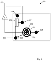
- Figure 1 shows an example plan view of a known semiconductor FET device in a charge-sensitive amplifier 600.
- the device is formed upon a silicon substrate in this case.
- the FET has an approximately circular region which acts as the drain of the FET.
- An aluminium drain pad 601 is placed upon the surface of the FET over this region.
- a gate electrode 602. Surrounding the drain pad and spaced therefrom in a concentric manner is a gate electrode 602. This is electrically connected via a short aluminium trace to a gate pad 603.
- a third electrode 604 is provided in a concentric manner around the gate electrode (and again, spaced therefrom), this being connected via a short trace to a source pad 605.
- a capacitor 606 is also provided, this having one "plate” connected via a trace to the gate pad 603 (and therefore to the gate electrode 602).
- a second plate of the capacitor 606 is connected via a short trace to a feedback pad 607.
- a substrate pad 608 is also provided to allow electrical connection to the silicon substrate for providing an appropriate potential.
- a further reset structure may be provided as in the MX-30 device mentioned earlier but this detail is not shown.
- the various pads allow electrical connection of wires to the device 600.
- signals from the detector such as an SDD are received at the input 609 and at the gate and are amplified by the amplifier A, resulting in an output 610 which is coupled via the capacitor 606 to the gate.
- the presence of the gate pad 603 generates a capacitance as part of the device.
- the feedback capacitor can be a discrete component but it can also be integrated on to the FET die and an example is shown in Figure 1 where the bond pad 607 for the feedback connection is connected to the long structure which is the feedback capacitor 606, this being connected by another thin track to the gate bond pad 603.
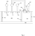
- the feedback capacitor may be implemented within an isolated region of semiconductor silicon. As illustrated in Figure 2 , a region 701 of typically n-type silicon is isolated from the rest of the device by p+ walls 702 that connect through to the p+ substrate 703 beneath. A conductive n+ region 704 forms one electrode of the feedback capacitor and is connected via a feedback bond pad 607 to the low impedance output of the external amplifier. A layer of oxide 706 provides the dielectric insulation for the top plate 707 of the capacitor 606 that is connected by a trace to the gate electrode 603.
- the electrode 704 will be electrically isolated from the substrate because of depletion of the semiconductor junction between n- silicon in region 701 and the p+ substrate 703. Therefore, fluctuations in the output voltage driven by the low impedance amplifier are coupled to the gate through the parallel plate feedback capacitor.
- the FET itself is formed in a nearby region of silicon. Specifically in Figure 2 this is formed from an n- type region of silicon 708 isolated by the p+ doped substrate 703 and side walls 702. Two heavily doped (n+) regions 709, 710 provide the source and drain respectively, separated by an intermediate region of p+ doped material 711 which acts as a gate. Bond pads 601, 603, 605, 607 and associated traces are indicated showing the electrical arrangement in accordance with Figure 1 .
- the gate electrode is a thin structure, often in the form of a ring about 2 micrometres wide so it is not large enough to have a bond pad attached to it directly since such a bond pad needs to be typically 70 micrometres in diameter or larger.
- the gate pad is on top of oxide, there is invariably a conductive structure beneath it.
- This conductive structure might be the p+ substrate as shown in Figure 2 , which is conductive and in a 4 terminal device it is held at a fixed voltage and the voltage supply is decoupled to ground to remove any AC noise fluctuations that would otherwise be amplified by the FET.
- part of the conductive structure could be the source n+ region, or the drain n+ region and these have low impedance to ground compared to the gate.
- the step in voltage on the gate is inversely proportional to the sum of all capacitances connected to the gate.
- Noise in the amplifier can be expressed as an equivalent voltage source at the gate and this noise is therefore equivalent to a noise charge source that is proportional to the sum of all capacitances connected to the gate. Therefore, the noise charge relative to the signal charge from the detector is proportional to the total of all capacitances connected to the gate. Since the feedback capacitor is an essential part of the charge sensitive configuration, if the gate bond pad is integrated with the feedback capacitor, then this saves the additional parasitic capacitance of the bond pad which would otherwise increase the total capacitance and noise.
- a bond pad is implemented by depositing Al metal on top of an oxide insulation layer on top of the p+ silicon substrate and a metal track connects the bond pad to the FET gate (see Figure 1 ).
- the top feedback capacitor electrode metal is configured in the shape of a bond pad, then the wire bond can be connected to the top of the feedback capacitor and a metal trace can connect the pad directly to the gate electrode.
- the two functions are integrated into one structure. In this case, the spurious capacitance of a dedicated gate bond pad is avoided.
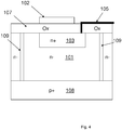
- FIG. 3 and Figure 4 An example of such an arrangement according to the invention is shown in Figure 3 and Figure 4 where the design of Figure 1 has been modified to incorporate the improvement provided by the combined gate pad and capacitor.
- the gate bond pad would be on top of field oxide on top of p+ implanted substrate material and would therefore have a parasitic capacitance to ground.
- the fabrication process is modified to isolate certain regions of n- silicon with p+ walls connecting to the p+ substrate beneath.
- a region of n- silicon 101 is shown in Figure 3 beneath the gate bond pad 102.
- the p+ substrate is illustrated at 108 in Figure 4 , with the p+ walls being denoted 109.
- an n+ surface layer 103 is created within the n- region 101.
- a layer of oxide 107 is positioned above the n+ layer 103.
- the gate bond pad 102 is formed from aluminium placed upon the layer of oxide 107, the oxide thereby forming the dielectric for the capacitor. Note that a reset structure may also be included but this has been omitted for clarity. It is noted here that this arrangement according to the example may be used to replace the arrangement shown in Figure 1 (whilst retaining the amplifier A and other associated electronics) to realise a charge-sensitive amplifier with a discrete FET having reduced parasitic capacitance.
- the feedback bond pad 104 (see Figure 1 ) is electrically connected by a metal trace 105 to the n+ layer 103 and the aluminium gate bond pad 102 is built on top of the oxide 107 so that the gate bond pad, oxide and underlying n+ region form a parallel plate capacitor.
- Oxide 107 can be field oxide or oxide specifically constructed in the region of the capacitor. Since the feedback connection is normally connected to a low impedance amplifier output, the n+ layer 103 beneath the gate bond pad effectively screens the gate bond pad from the p+ Si substrate so there is no parasitic capacitance to ground.
- the effective feedback capacitance is about 0.13pF. Larger values of feedback capacitance can be made (such as 0.3pF) by extending the area of the bond pad. Smaller feedback capacitances can be achieved by increasing the thickness of oxide underneath the bond pad but there may be practical constraints, such as fabrication capability, amplifier stability and sensitivity to parasitic capacitances, that limit how small this capacitance can be.
- a feedback capacitor is essential. By integrating the feedback capacitor into the gate bond pad structure required for wire bonding, the parasitic capacitance of the gate bond pad can be avoided and this improves the noise performance of a radiation detector.
- the principle of the invention can be applied to any semiconductor FET that gives the first stage of amplification for a radiation detector.
- the polarities of n-type and p-type materials can be reversed and other semiconductors other than Si could be used in principle.
- the invention is primarily aimed at x-ray detection systems using an SDD, the principle can be applied for detection of any energetic particle that liberates an increment of electronic charge that needs to be amplified with a charge sensitive amplifier configuration.
- many types of radiation detector for x-rays, gamma-rays, optical photons, electrons and ions could benefit.
Description
- The present invention relates to the field of radiation detection and imaging. In particular, the present invention relates to an apparatus for improving the performance of semiconductor radiation detectors for detection and measurement of energetic particles, such as x-ray photons. The inventive apparatus is in the form of a charge-sensitive amplifier for use in amplifying signals from a particle detector. The present invention finds particular advantage in x-ray detection systems where a Field Effect Transistor (FET) is bonded to a semiconductor detector element and used in a "charge-sensitive" amplifier configuration. The invention provides a method to reduce the overall capacitance and thus improve the resolution of the detector as a whole.
- For the last 40 years there has been ongoing development of semiconductor radiation detectors to achieve increased sensitivity, higher energy resolution, lower electronic noise and larger active area. The last 10 years has seen the emergence of a new type of commercially available detector, the "silicon drift detector" (SDD) which differs from previous types of detector such as PIN diodes and lithium-compensated (Si(Li)) detectors by virtue of having an anode capacitance typically less than 0.2pF. This SDD capacitance is more than an order of magnitude smaller than that of the previous types.
- For best detection results, it is important to optimise the interface between the detector and readout electronics and in particular the connection to the field effect transistor, FET, that is used to form the first amplification stage. The noise performance of the detector and FET combination depends on the total capacitance "seen" at the gate of the FET. This includes the detector capacitance, the input capacitance of the FET and any other capacitances effectively connected to the gate (see for example, Sonsky et al Nucl.lnstrum.and Methods in Physics Research A 517, 2004, 301-312, eqn.2 and section 5.1).
- For many years, discrete FETs have been commercially available that offer high gain and excellent noise performance and are ideal for use with PIN diode and Si(Li) detectors. These FETs typically have capacitances below 1pF (see for example the URL http://www.moxtek.com/jfets/ultra-low-noise-jfets.html and the associated "N-Channel Ultra-Low Noise JFETS CATALOG").
- Discrete FETs can in principle be made with much smaller input capacitance than 1pF but when the FET input capacitance is reduced by shrinking the dimensions of the FET, this also reduces the FET gain. Therefore, for optimum performance with a particular type of FET, the input capacitance of the FET needs to be close to the sum of detector capacitance and all other capacitances effectively connected to the gate. The gate contact for a discrete FET needs to be connected to the detector and this is commonly achieved by using standard wire bonding techniques where a short wire is bonded at one end to the readout anode of the detector and, at the other end, to the FET gate.
- Round bond pads are used in a typical discrete FET designed for use in radiation detectors (see for example the "MX-30" discussed at the above URL). Each bond pad is a round structure connected by a thin "trace" (also called a "track") to the required electrode (such as "substrate", "feedback", "source", "drain", "gate", "reset"). In the industry such pads are normally made of aluminium metal using conventional semiconductor lithography and are placed on top of "field oxide" that is typically 1 micrometre thick which electrically insulates the metal pad from the silicon material beneath. In an n-channel JFET the silicon material underneath would typically be the p+ material of the substrate that is held at a fixed potential. The bond pad has to be large enough to make a wire bond connection using a "wedge" or "ball" bonder and for convenience, most non-critical bond pads will be around 100 micrometres in diameter. If a pad is made smaller it makes it harder to position the wire bond within the boundary of the pad. With commonly-available bonding equipment, it is difficult to work with bond pads that have diameter smaller than 70 micrometres.
- The material beneath the oxide is effectively a ground plane for signals and a circular bond pad with 70um diameter on top of 1 micrometre of silicon dioxide gives an effective "parallel plate" capacitance to ground of 0.13pF. Thus, for an SDD detector, the stray capacitance introduced by the critical gate bond pad can be larger than the detector capacitance. This stray capacitance effectively sets a lower limit on the capacitance of a discrete FET because in practice it is not worth reducing the dimensions of the discrete FET to the point where the reduction in noise, due to reduction in total capacitance, is outweighed by the increase in noise due to loss in gain of the FET.
- In order to avoid the need for a bond pad and wire connection, the FET of the first amplifying stage can be integrated on to the same silicon as the detector chip (e.g. see the earlier cited reference Sonsky et al 2004). However, when this approach is used, it is difficult to design and fabricate a suitable FET that will produce the desired characteristics because the technological processes and materials for fabricating FETs with good amplification and noise properties are usually quite different from those that are required for semiconductor radiation detectors made on high resistivity silicon. Thus, the integration of the FET on the same substrate as the detector is highly desirable in principle but has some practical difficulties.
- Fiorini C. et al., "Charge-Sensitive Preamplifier with Continuous Reset by Means of the Gate-to-Drain Current of the JFET Integrated on the Detector", XP002364505, 2002 discloses a preamplifier wherein an input n-JFET and a feedback are integrated directly on a detector chip.
- The difference between integrated and discrete FETs is well known. For example, Niculae et al Microsc Microanal 13(Suppl 2), 2007, point out (with reference to their
Figure 1b ) that the bonding pad required for a discrete FET adds additional input capacitance. - Since there are some advantages in retaining a discrete FET, it would be desirable to find a way of avoiding the disadvantage of the parasitic bond pad capacitance associated with wire bonding. It is in this context that the invention is provided.
- In accordance with a first aspect of the present invention we provide a charge-sensitive amplifier for use in amplifying signals from a particle detector, the charge-sensitive amplifier comprising a field effect transistor having a gate, source and drain, the gate being connectable, using a wire bond and gate bond pad, to the particle detector, for the receipt of said signals; an amplifier having an input connected to the drain or source of the field effect transistor and an output connected through a feedback capacitor to the gate of the field effect transistor, characterised in that the plate of the feedback capacitor that is connected to the low impedance amplifier output electromagnetically shields the gate bond pad from the substrate such that parasitic capacitance attributable to the gate bond pad is effectively removed or made substantially less than the total capacitance experienced at the gate.
- We have therefore realised that by making the gate pad of the field effect transistor integral with the feedback capacitor it is possible to effectively remove the capacitance attributable to the gate pad itself, whilst retaining the gate pad and capacitor functionality. The inventive arrangement avoids the gate bond pad effectively making a capacitive connection with anything other than the feedback signal which is driven by the low impedance amplifier output.
- In order to achieve this, typically the feedback capacitor comprises a plurality of capacitor plates separated by a dielectric region wherein the gate pad forms at least part of one of the said plates. Thus an integral or combined gate pad-capacitor component is formed by the use of the conductive gate pad as one of the capacitor plates. A typical thickness for the dielectric region, in terms of providing a separation distance between the "plates", is about 0.5 to 1 micrometre. In the case of a silicon substrate the dielectric is typically silicon dioxide.
- Where one of the capacitor plates is provided by the gate pad, another of said plates is preferably in the form of a highly doped extrinsic semiconductor material. In the case of an n-doped material, such a region would be denoted n+ for example.
- As will be appreciated, the gate pad is typically arranged at a generally planar surface of the field effect transistor and the capacitor is formed at least partially beneath the said gate pad with respect to the said surface. The gate pad may extend uniformly in all radial directions with respect to the said surface and therefore be generally circular in shape with respect to the surface. Other shapes are also contemplated such as oval and rectangular shapes. It is therefore possible to shape the pad slightly to reduce the total area, by making it more rectangular or oval. When a "wedge bonder" is used, this is generally easier to position side-to-side but more difficult to position the bond in the direction of the wire. A further consideration is that there is a bond "tail" in the direction of the wire.
- It is preferred that a generally similar shape is adopted by the region of material forming the other plate beneath the gate pad (such as the highly doped extrinsic semiconductor). In general, the structures forming the capacitor plates are isolated by a surrounding region of semiconductor material. For example this material may be relatively lightly doped extrinsic semiconductor material which in the case of n-doping would be referred to as n-. A "trace" (or "track") is preferably provided to connect the highly doped semiconductor material forming the other plate to a laterally spaced apart feedback pad provided upon the aforementioned surface. The feedback pad may take a known form such as a circular deposit of aluminium material.
- Thus the charge-sensitive amplifier may comprise a region of extrinsic semiconductor material positioned beneath the highly doped region forming one of the capacitor plates, the said region beneath the plates having a relatively low doping level in comparison with the said highly doped region. Each of the relatively low and high doped regions are formed from a similar semiconductor doping type in this case. Such types include "n" and "p" types as is known in the art.
- In most cases the charge-sensitive amplifier comprises a substrate positioned beneath the region of relatively low doping, the substrate being formed from a highly doped extrinsic semiconductor material of a second type, different from the first. This may be electrically biased when in use to ensure electrical isolation at the "pn" junction region between the first and second types. An electrical connection to such a substrate may also be provided using a pad deposited upon the surface of the field effect transistor. The effect of the relative position of the highly doped capacitor plate therefore provides electromagnetic shielding of the gate pad from the substrate. Thus the relative arrangement of the gate pad and capacitor causes a capacitance between the gate pad and the "ground" to be substantially less than the total capacitance experienced at the gate.
- The charge-sensitive amplifier may be arranged in two possible alternative configurations. It may be firstly connected to the field effect transistor in a "source follower" configuration in which the amplifier is connected to the source. It may alternatively be connected in a "common source configuration" in which the amplifier is connected to the drain of the field effect transistor.
- The invention is not intended to be limited to any specific type of field effect transistor and therefore it may be implemented with each of JFET or MOSFET devices. Thus it will be appreciated, the present invention finds particular application in arrangements wherein the total capacitance of the detector and all other capacitances effectively connected to the gate of the field effect transistor are less than 1pF.
- In addition to the charge-sensitive amplifier according to the first aspect of the present invention, we also provide, in accordance with a second aspect of the invention, a particle analyser system comprising a charge-sensitive amplifier according to the first aspect and a particle detector having an output arranged to provide signals representative of detected particles for signal amplification by the charge-sensitive amplifier. It is preferred that the particle detector in question is a silicon drift detector although it will be appreciated that other types of particle detector may be used. A number of different particle types may be detected using such a system depending upon the specific implementation, although it is preferred that the system is used in the detection of x-ray photons. It will be appreciated that each of the said field effect transistor, amplifier and the detector are typically arranged a discrete components which are electrically connected when in use by wires bonded to respective bond pads, one of the said bond pads being the said gate pad.
- The abovementioned therefore provides the advantages associated with the use of discrete field effect transistors including optimising manufacturing productivity whilst at the same time delivering benefits analogous to detector chips having integrated field effect transistors.
- An example of a charge-sensitive amplifier according to the present invention is now described with reference to the accompanying drawings, in which:-
-
Figure 1 is an example plan view of a known field effect transistor device incorporating separate feedback and gate pads; -
Figure 2 shows a schematic section through such a known field effect transistor device with associated capacitor; -
Figure 3 shows a schematic plan view of an example arrangement according to the invention; and, -
Figure 4 shows a schematic section through the combined gate pad and capacitor according to the example. - The invention exploits a feature which is commonly used in radiation detection systems to achieve a "charge sensitive amplifier" (CSA). The output voltage step from a CSA is proportional to the increment of charge deposited at the input and is independent of the capacitance of the detector connected to the input. Since the increment of charge released by the detector is proportional to the energy of the incident radiation particle, the output voltage step from a CSA is also proportional to the energy of the particle. An example of such a CSA is described in
GB 2305776 GB 2305776 - The FET device is typically a small die with dimension approximately 1mm by 1mm and connections to the electrodes of the FET are typically made by wire bonding to bond pads as described earlier.
-
Figure 1 shows an example plan view of a known semiconductor FET device in a charge-sensitive amplifier 600. The device is formed upon a silicon substrate in this case. The FET has an approximately circular region which acts as the drain of the FET. Analuminium drain pad 601 is placed upon the surface of the FET over this region. Surrounding the drain pad and spaced therefrom in a concentric manner is agate electrode 602. This is electrically connected via a short aluminium trace to agate pad 603. Athird electrode 604 is provided in a concentric manner around the gate electrode (and again, spaced therefrom), this being connected via a short trace to asource pad 605. Acapacitor 606 is also provided, this having one "plate" connected via a trace to the gate pad 603 (and therefore to the gate electrode 602). A second plate of thecapacitor 606 is connected via a short trace to afeedback pad 607. Asubstrate pad 608 is also provided to allow electrical connection to the silicon substrate for providing an appropriate potential. A further reset structure may be provided as in the MX-30 device mentioned earlier but this detail is not shown. - The various pads allow electrical connection of wires to the
device 600. In use, signals from the detector such as an SDD are received at theinput 609 and at the gate and are amplified by the amplifier A, resulting in anoutput 610 which is coupled via thecapacitor 606 to the gate. As described earlier however, the presence of thegate pad 603 generates a capacitance as part of the device. - The feedback capacitor can be a discrete component but it can also be integrated on to the FET die and an example is shown in
Figure 1 where thebond pad 607 for the feedback connection is connected to the long structure which is thefeedback capacitor 606, this being connected by another thin track to thegate bond pad 603. - The feedback capacitor may be implemented within an isolated region of semiconductor silicon. As illustrated in
Figure 2 , aregion 701 of typically n-type silicon is isolated from the rest of the device by p+walls 702 that connect through to thep+ substrate 703 beneath. Aconductive n+ region 704 forms one electrode of the feedback capacitor and is connected via afeedback bond pad 607 to the low impedance output of the external amplifier. A layer ofoxide 706 provides the dielectric insulation for thetop plate 707 of thecapacitor 606 that is connected by a trace to thegate electrode 603. Provided the voltage of the p+ substrate is held at a more negative potential than the feedback amplifier output, theelectrode 704 will be electrically isolated from the substrate because of depletion of the semiconductor junction between n- silicon inregion 701 and thep+ substrate 703. Therefore, fluctuations in the output voltage driven by the low impedance amplifier are coupled to the gate through the parallel plate feedback capacitor. - The FET itself is formed in a nearby region of silicon. Specifically in
Figure 2 this is formed from an n- type region ofsilicon 708 isolated by the p+ dopedsubstrate 703 andside walls 702. Two heavily doped (n+)regions doped material 711 which acts as a gate.Bond pads Figure 1 . - It will be appreciated that the gate electrode is a thin structure, often in the form of a ring about 2 micrometres wide so it is not large enough to have a bond pad attached to it directly since such a bond pad needs to be typically 70 micrometres in diameter or larger. If the gate pad is on top of oxide, there is invariably a conductive structure beneath it. This conductive structure might be the p+ substrate as shown in
Figure 2 , which is conductive and in a 4 terminal device it is held at a fixed voltage and the voltage supply is decoupled to ground to remove any AC noise fluctuations that would otherwise be amplified by the FET. Under the oxide, part of the conductive structure could be the source n+ region, or the drain n+ region and these have low impedance to ground compared to the gate. Thus, when an increment of charge appears at the gate, the step in voltage on the gate is inversely proportional to the sum of all capacitances connected to the gate. Noise in the amplifier can be expressed as an equivalent voltage source at the gate and this noise is therefore equivalent to a noise charge source that is proportional to the sum of all capacitances connected to the gate. Therefore, the noise charge relative to the signal charge from the detector is proportional to the total of all capacitances connected to the gate. Since the feedback capacitor is an essential part of the charge sensitive configuration, if the gate bond pad is integrated with the feedback capacitor, then this saves the additional parasitic capacitance of the bond pad which would otherwise increase the total capacitance and noise. - In the known arrangement, normally, a bond pad is implemented by depositing Al metal on top of an oxide insulation layer on top of the p+ silicon substrate and a metal track connects the bond pad to the FET gate (see
Figure 1 ). However, as realised by the present invention, if the top feedback capacitor electrode metal is configured in the shape of a bond pad, then the wire bond can be connected to the top of the feedback capacitor and a metal trace can connect the pad directly to the gate electrode. Thus, rather than have a separate feedback capacitor and bond pad, the two functions are integrated into one structure. In this case, the spurious capacitance of a dedicated gate bond pad is avoided. - An example of such an arrangement according to the invention is shown in
Figure 3 andFigure 4 where the design ofFigure 1 has been modified to incorporate the improvement provided by the combined gate pad and capacitor. In the example discussed earlier, according to the prior design, the gate bond pad would be on top of field oxide on top of p+ implanted substrate material and would therefore have a parasitic capacitance to ground. In the modified device ofFigure 3 according to this example the fabrication process is modified to isolate certain regions of n- silicon with p+ walls connecting to the p+ substrate beneath. In particular, a region of n-silicon 101 is shown inFigure 3 beneath thegate bond pad 102. The p+ substrate is illustrated at 108 inFigure 4 , with the p+ walls being denoted 109. Subsequently, ann+ surface layer 103 is created within the n-region 101. A layer ofoxide 107 is positioned above then+ layer 103. Thegate bond pad 102 is formed from aluminium placed upon the layer ofoxide 107, the oxide thereby forming the dielectric for the capacitor. Note that a reset structure may also be included but this has been omitted for clarity. It is noted here that this arrangement according to the example may be used to replace the arrangement shown inFigure 1 (whilst retaining the amplifier A and other associated electronics) to realise a charge-sensitive amplifier with a discrete FET having reduced parasitic capacitance. - Using conventional semiconductor lithographic processes, the feedback bond pad 104 (see
Figure 1 ) is electrically connected by ametal trace 105 to then+ layer 103 and the aluminiumgate bond pad 102 is built on top of theoxide 107 so that the gate bond pad, oxide and underlying n+ region form a parallel plate capacitor.Oxide 107 can be field oxide or oxide specifically constructed in the region of the capacitor. Since the feedback connection is normally connected to a low impedance amplifier output, then+ layer 103 beneath the gate bond pad effectively screens the gate bond pad from the p+ Si substrate so there is no parasitic capacitance to ground. - If the oxide is 1 micrometre thick and the gate bond pad is 70 micrometres in diameter then the effective feedback capacitance is about 0.13pF. Larger values of feedback capacitance can be made (such as 0.3pF) by extending the area of the bond pad. Smaller feedback capacitances can be achieved by increasing the thickness of oxide underneath the bond pad but there may be practical constraints, such as fabrication capability, amplifier stability and sensitivity to parasitic capacitances, that limit how small this capacitance can be.
- In detector amplification systems that require a charge sensitive amplifier configuration, a feedback capacitor is essential. By integrating the feedback capacitor into the gate bond pad structure required for wire bonding, the parasitic capacitance of the gate bond pad can be avoided and this improves the noise performance of a radiation detector.
- The principle of the invention can be applied to any semiconductor FET that gives the first stage of amplification for a radiation detector. The polarities of n-type and p-type materials can be reversed and other semiconductors other than Si could be used in principle. Although the invention is primarily aimed at x-ray detection systems using an SDD, the principle can be applied for detection of any energetic particle that liberates an increment of electronic charge that needs to be amplified with a charge sensitive amplifier configuration. Thus, many types of radiation detector for x-rays, gamma-rays, optical photons, electrons and ions could benefit.
Claims (17)
- A charge-sensitive amplifier for use in amplifying signals from a particle detector, the charge-sensitive amplifier comprising:-a field effect transistor having a gate, source and drain, the gate being connectable, using a wire bond and gate bond pad (102), to the particle detector, for the receipt of said signals;an amplifier having an input connected to the drain or source of the field effect transistor and a low impedance output connected through a feedback capacitor to the gate of the field effect transistor, characterised in that a plate of the feedback capacitor that is connected to the low impedance amplifier output is positioned to electromagnetically shield the gate bond pad (102) from a substrate (108) underneath the gate bond pad (102) such that parasitic capacitance attributable to the gate bond pad (102) is effectively removed or made substantially less than a total capacitance at the gate.
- A charge-sensitive amplifier according to claim 1, wherein the feedback capacitor comprises a plurality of capacitor plates separated by a dielectric region and wherein the gate bond pad (102) forms at least part of one of the said plates.
- A charge-sensitive amplifier according to claim 2, wherein the dielectric region is arranged to provide a separation between the plates of the capacitor of at least 0.5um.
- A charge-sensitive amplifier according to claim 2 or claim 3, wherein another of said plurality of capacitor plates is formed from a highly doped extrinsic semiconductor material.
- A charge-sensitive amplifier according to claim 4, wherein the gate bond pad (102) is arranged at a generally planar surface of the field effect transistor and wherein the capacitor is formed at least partially beneath said gate bond pad with respect to said surface.
- A charge-sensitive amplifier according to claim 5, wherein the capacitor plates are isolated by a surrounding region of semiconductor material.
- A charge-sensitive amplifier according to claim 5 or claim 6, wherein a trace (105) is provided to connect the said highly doped semiconductor material forming the said another plate to a laterally spaced apart feedback pad (104) provided upon the said surface.
- A charge-sensitive amplifier according to any of claims 4 to 7, wherein charge sensitive amplifier comprises a region of extrinsic semiconductor material, positioned beneath the highly doped region and having a relatively low doping level in comparison with the said highly doped region, each of the relatively low and highly doped regions being of a first semiconductor doping type.
- A charge-sensitive amplifier according to claim 8, further comprising a substrate positioned beneath the low doping region, the said substrate being formed from a highly doped extrinsic semiconductor material of a second type, different from the first.
- A charge-sensitive amplified according to claim 9, wherein the relative position of the highly doped capacitor plate provides electromagnetic shielding of the gate bond pad (102) from the substrate.
- A charge-sensitive amplifier according to any of the preceding claims, wherein when the amplifier is connected to the field effect transistor in a source follower configuration in which the amplifier is connected to the source, or a common source configuration in which the amplifier is connected to the drain.
- A charge-sensitive amplifier according to any of the preceding claims, wherein the field effect transistor is a JFET or a MOSFET.
- A charge-sensitive amplifier according to any of the preceding claims, wherein the relative arrangement of the gate bond pad (102) and capacitor causes the capacitance between the gate bond pad and the ground to be substantially less than the total capacitance at the gate.
- A charge-sensitive amplifier according to claim 14, wherein the total capacitance between the gate bond pad (102) and the ground is less than 1pF.
- A particle analyser system comprising:-a charge-sensitive amplifier according to any of the preceding claims; anda particle detector having an output arranged to provide signals representative of detected particles for signal amplification by the charge-sensitive amplifier.
- A particle analyser system according to claim 16, where in the particle detector is a silicon drift detector.
- A particle analyser system according to claim 16 or 17, wherein each of the said field effect transistor, the amplifier and the detector are separate components which are electrically connected when in use, by wires bonded to respective bond pads, one of the said bond pads being the said gate bond pad (102).
Priority Applications (1)
| Application Number | Priority Date | Filing Date | Title |
|---|---|---|---|
| PL12725134T PL2710733T3 (en) | 2011-05-19 | 2012-05-17 | Charge-sensitive amplifier |
Applications Claiming Priority (2)
| Application Number | Priority Date | Filing Date | Title |
|---|---|---|---|
| GB1108420.9A GB2491111B (en) | 2011-05-19 | 2011-05-19 | Charge-sensitive amplifier |
| PCT/GB2012/051114 WO2012156748A1 (en) | 2011-05-19 | 2012-05-17 | Charge-sensitive amplifier |
Publications (2)
| Publication Number | Publication Date |
|---|---|
| EP2710733A1 EP2710733A1 (en) | 2014-03-26 |
| EP2710733B1 true EP2710733B1 (en) | 2018-06-20 |
Family
ID=44279298
Family Applications (1)
| Application Number | Title | Priority Date | Filing Date |
|---|---|---|---|
| EP12725134.6A Active EP2710733B1 (en) | 2011-05-19 | 2012-05-17 | Charge-sensitive amplifier |
Country Status (6)
| Country | Link |
|---|---|
| US (1) | US9397626B2 (en) |
| EP (1) | EP2710733B1 (en) |
| JP (3) | JP6441675B2 (en) |
| GB (1) | GB2491111B (en) |
| PL (1) | PL2710733T3 (en) |
| WO (1) | WO2012156748A1 (en) |
Families Citing this family (6)
| Publication number | Priority date | Publication date | Assignee | Title |
|---|---|---|---|---|
| WO2014021358A1 (en) * | 2012-08-02 | 2014-02-06 | 株式会社堀場製作所 | Amplifier and radiation detector |
| CN106190340B (en) * | 2016-07-19 | 2019-07-12 | 太原理工大学 | Renewable metal composite oxide desulfurizing agent for high-temp gas and preparation method |
| US10126437B1 (en) * | 2017-05-15 | 2018-11-13 | Prismatic Sensors Ab | Detector for x-ray imaging |
| CN107677723B (en) * | 2017-09-25 | 2023-06-30 | 付德君 | Method and device for measuring mass spectrum of gas cluster ion beam |
| IT201800010671A1 (en) * | 2018-11-29 | 2020-05-29 | Milano Politecnico | CHARGING PRE-AMPLIFIER DEVICE AND RADIATION DETECTION DEVICE INCLUDING THE DEVICE |
| CN115021696B (en) * | 2022-08-02 | 2023-06-27 | 宁波中车时代传感技术有限公司 | Charge amplifier circuit and vibration sensor |
Citations (1)
| Publication number | Priority date | Publication date | Assignee | Title |
|---|---|---|---|---|
| US20020113287A1 (en) * | 1998-07-15 | 2002-08-22 | Sang-Heon Lee | Semiconductor integrated circuit device with capacitor formed under bonding pad |
Family Cites Families (20)
| Publication number | Priority date | Publication date | Assignee | Title |
|---|---|---|---|---|
| US4211941A (en) * | 1978-08-03 | 1980-07-08 | Rca Corporation | Integrated circuitry including low-leakage capacitance |
| JPS6153756A (en) * | 1984-08-24 | 1986-03-17 | Hitachi Ltd | Semiconductor device |
| US4949150A (en) * | 1986-04-17 | 1990-08-14 | Exar Corporation | Programmable bonding pad with sandwiched silicon oxide and silicon nitride layers |
| US4829017A (en) * | 1986-09-25 | 1989-05-09 | Texas Instruments Incorporated | Method for lubricating a high capacity dram cell |
| US4761385A (en) * | 1987-02-10 | 1988-08-02 | Motorola, Inc. | Forming a trench capacitor |
| GB8800949D0 (en) * | 1988-01-16 | 1988-02-17 | Link Analytical Ltd | Junction field effect transistors |
| US5170229A (en) * | 1988-01-16 | 1992-12-08 | Link Analytical Limited | Junction field effect transistors with injector region |
| US5166679A (en) * | 1991-06-06 | 1992-11-24 | The United States Of America As Represented By The Administrator Of The National Aeronautics & Space Administration | Driven shielding capacitive proximity sensor |
| TW291595B (en) * | 1995-05-30 | 1996-11-21 | At & T Corp | |
| GB2305776B (en) * | 1995-09-28 | 1999-11-17 | Gresham Sensor Technology Limi | Charge amplifier |
| US6137138A (en) * | 1998-03-06 | 2000-10-24 | Spectrian Corporation | MOSFET power transistor having offset gate and drain pads to reduce capacitance |
| JP4124867B2 (en) * | 1998-07-14 | 2008-07-23 | 松下電器産業株式会社 | Conversion device |
| US6690251B2 (en) * | 2001-04-11 | 2004-02-10 | Kyocera Wireless Corporation | Tunable ferro-electric filter |
| US6587003B2 (en) | 2001-04-18 | 2003-07-01 | Canberra Industries. Inc. | Charge sensitive preamplifier with pulsed source reset |
| GB0125661D0 (en) | 2001-10-25 | 2001-12-19 | Council Cent Lab Res Councils | Amplifiers |
| US7193216B2 (en) * | 2004-10-22 | 2007-03-20 | Oxford Instruments Analytical Oy | Method and circuit arrangement for compensating for rate dependent change of conversion factor in a drift-type radiation detector and a detector appliance |
| JP4672539B2 (en) * | 2005-12-06 | 2011-04-20 | パナソニック株式会社 | Condenser microphone device |
| GB2466776A (en) * | 2008-12-30 | 2010-07-07 | Wolfson Microelectronics Plc | Bootstrapping to reduce the effect of bond pad parasitic capacitance in a MEMS microphone circuit |
| US8058674B2 (en) | 2009-10-07 | 2011-11-15 | Moxtek, Inc. | Alternate 4-terminal JFET geometry to reduce gate to source capacitance |
| WO2014021358A1 (en) * | 2012-08-02 | 2014-02-06 | 株式会社堀場製作所 | Amplifier and radiation detector |
-
2011
- 2011-05-19 GB GB1108420.9A patent/GB2491111B/en active Active
-
2012
- 2012-05-07 US US14/118,492 patent/US9397626B2/en active Active
- 2012-05-17 PL PL12725134T patent/PL2710733T3/en unknown
- 2012-05-17 WO PCT/GB2012/051114 patent/WO2012156748A1/en active Application Filing
- 2012-05-17 EP EP12725134.6A patent/EP2710733B1/en active Active
- 2012-05-17 JP JP2014510883A patent/JP6441675B2/en active Active
-
2017
- 2017-01-12 JP JP2017003400A patent/JP6393347B2/en not_active Expired - Fee Related
-
2018
- 2018-06-12 JP JP2018111654A patent/JP2018137828A/en active Pending
Patent Citations (1)
| Publication number | Priority date | Publication date | Assignee | Title |
|---|---|---|---|---|
| US20020113287A1 (en) * | 1998-07-15 | 2002-08-22 | Sang-Heon Lee | Semiconductor integrated circuit device with capacitor formed under bonding pad |
Non-Patent Citations (1)
| Title |
|---|
| FIORINI C ET AL: "Charge-sensitive preamplifier with continuous reset by means of the gate-to-drain current of the JFET integrated on the detector", IEEE TRANSACTIONS ON NUCLEAR SCIENCE, IEEE SERVICE CENTER, NEW YORK, NY, US, vol. 49, no. 3, 1 June 2002 (2002-06-01), pages 1147 - 1151, XP002364505, ISSN: 0018-9499, DOI: 10.1109/TNS.2002.1039628 * |
Also Published As
| Publication number | Publication date |
|---|---|
| GB201108420D0 (en) | 2011-07-06 |
| EP2710733A1 (en) | 2014-03-26 |
| US9397626B2 (en) | 2016-07-19 |
| GB2491111A (en) | 2012-11-28 |
| WO2012156748A1 (en) | 2012-11-22 |
| PL2710733T3 (en) | 2018-11-30 |
| JP6393347B2 (en) | 2018-09-19 |
| JP2017098996A (en) | 2017-06-01 |
| US20150030132A1 (en) | 2015-01-29 |
| JP2014519261A (en) | 2014-08-07 |
| JP6441675B2 (en) | 2018-12-19 |
| GB2491111B (en) | 2015-08-19 |
| JP2018137828A (en) | 2018-08-30 |
Similar Documents
| Publication | Publication Date | Title |
|---|---|---|
| EP2710733B1 (en) | Charge-sensitive amplifier | |
| US6455858B1 (en) | Semiconductor radiation detector | |
| US9461080B2 (en) | Semiconductor device for radiation detection | |
| EP2808705B1 (en) | Semiconductor detector with radiation shield | |
| US20220216245A1 (en) | Avalanche photodiode array | |
| KR20080085155A (en) | Semiconductor radiation detector optimized for detecting visible light | |
| JP2014519261A5 (en) | ||
| US6522012B2 (en) | Semiconductor device with HIHG resistivity | |
| EP3701571B1 (en) | Integrated sensor of ionizing radiation and ionizing particles | |
| JP2013145180A (en) | Radiation detector, radiation detection assembly and operation method thereof | |
| US11604292B2 (en) | Charge preamplifier device and radiation detecting apparatus comprising the device | |
| TW493073B (en) | A monolithic semiconductor detector | |
| TWI806960B (en) | light detection device | |
| JP5410901B2 (en) | Photodetector | |
| CN106783900B (en) | SOI pixel detector structure | |
| CN109904272B (en) | Pixel detector with high conversion gain and low crosstalk | |
| JPH11186285A (en) | Semiconductor device | |
| Arai | New techniques in SOI pixel detector | |
| US20230387149A1 (en) | Optical sensor | |
| US20050279920A1 (en) | Self-pixelating focal plane array with electronic output | |
| WO2020008531A1 (en) | X-ray detector | |
| CN112071874A (en) | Silicon drift detector and metal oxide semiconductor field effect transistor integrated device | |
| Safavi-Naeini et al. | Evaluation of silicon detectors with integrated JFET for biomedical applications | |
| WO1990005995A1 (en) | Semiconductor device | |
| CN114300570A (en) | Probe and method of manufacture |
Legal Events
| Date | Code | Title | Description |
|---|---|---|---|
| PUAI | Public reference made under article 153(3) epc to a published international application that has entered the european phase |
Free format text: ORIGINAL CODE: 0009012 |
|
| 17P | Request for examination filed |
Effective date: 20131216 |
|
| AK | Designated contracting states |
Kind code of ref document: A1 Designated state(s): AL AT BE BG CH CY CZ DE DK EE ES FI FR GB GR HR HU IE IS IT LI LT LU LV MC MK MT NL NO PL PT RO RS SE SI SK SM TR |
|
| DAX | Request for extension of the european patent (deleted) | ||
| 17Q | First examination report despatched |
Effective date: 20141016 |
|
| GRAP | Despatch of communication of intention to grant a patent |
Free format text: ORIGINAL CODE: EPIDOSNIGR1 |
|
| STAA | Information on the status of an ep patent application or granted ep patent |
Free format text: STATUS: GRANT OF PATENT IS INTENDED |
|
| INTG | Intention to grant announced |
Effective date: 20180223 |
|
| GRAS | Grant fee paid |
Free format text: ORIGINAL CODE: EPIDOSNIGR3 |
|
| RBV | Designated contracting states (corrected) |
Designated state(s): AL AT BE BG CH CY CZ DE DK EE ES FI FR GR HR HU IE IS IT LI LT LU LV MC MK MT NL NO PL PT RO RS SE SI SK SM TR |
|
| GRAA | (expected) grant |
Free format text: ORIGINAL CODE: 0009210 |
|
| STAA | Information on the status of an ep patent application or granted ep patent |
Free format text: STATUS: THE PATENT HAS BEEN GRANTED |
|
| AK | Designated contracting states |
Kind code of ref document: B1 Designated state(s): AL AT BE BG CH CY CZ DE DK EE ES FI FR GR HR HU IE IS IT LI LT LU LV MC MK MT NL NO PL PT RO RS SE SI SK SM TR |
|
| REG | Reference to a national code |
Ref country code: IE Ref legal event code: FG4D |
|
| REG | Reference to a national code |
Ref country code: DE Ref legal event code: R096 Ref document number: 602012047635 Country of ref document: DE |
|
| REG | Reference to a national code |
Ref country code: AT Ref legal event code: REF Ref document number: 1011279 Country of ref document: AT Kind code of ref document: T Effective date: 20180715 |
|
| REG | Reference to a national code |
Ref country code: NL Ref legal event code: MP Effective date: 20180620 |
|
| PG25 | Lapsed in a contracting state [announced via postgrant information from national office to epo] |
Ref country code: NO Free format text: LAPSE BECAUSE OF FAILURE TO SUBMIT A TRANSLATION OF THE DESCRIPTION OR TO PAY THE FEE WITHIN THE PRESCRIBED TIME-LIMIT Effective date: 20180920 Ref country code: LT Free format text: LAPSE BECAUSE OF FAILURE TO SUBMIT A TRANSLATION OF THE DESCRIPTION OR TO PAY THE FEE WITHIN THE PRESCRIBED TIME-LIMIT Effective date: 20180620 Ref country code: BG Free format text: LAPSE BECAUSE OF FAILURE TO SUBMIT A TRANSLATION OF THE DESCRIPTION OR TO PAY THE FEE WITHIN THE PRESCRIBED TIME-LIMIT Effective date: 20180920 Ref country code: SE Free format text: LAPSE BECAUSE OF FAILURE TO SUBMIT A TRANSLATION OF THE DESCRIPTION OR TO PAY THE FEE WITHIN THE PRESCRIBED TIME-LIMIT Effective date: 20180620 |
|
| REG | Reference to a national code |
Ref country code: LT Ref legal event code: MG4D |
|
| PG25 | Lapsed in a contracting state [announced via postgrant information from national office to epo] |
Ref country code: RS Free format text: LAPSE BECAUSE OF FAILURE TO SUBMIT A TRANSLATION OF THE DESCRIPTION OR TO PAY THE FEE WITHIN THE PRESCRIBED TIME-LIMIT Effective date: 20180620 Ref country code: LV Free format text: LAPSE BECAUSE OF FAILURE TO SUBMIT A TRANSLATION OF THE DESCRIPTION OR TO PAY THE FEE WITHIN THE PRESCRIBED TIME-LIMIT Effective date: 20180620 Ref country code: GR Free format text: LAPSE BECAUSE OF FAILURE TO SUBMIT A TRANSLATION OF THE DESCRIPTION OR TO PAY THE FEE WITHIN THE PRESCRIBED TIME-LIMIT Effective date: 20180921 Ref country code: HR Free format text: LAPSE BECAUSE OF FAILURE TO SUBMIT A TRANSLATION OF THE DESCRIPTION OR TO PAY THE FEE WITHIN THE PRESCRIBED TIME-LIMIT Effective date: 20180620 |
|
| REG | Reference to a national code |
Ref country code: AT Ref legal event code: MK05 Ref document number: 1011279 Country of ref document: AT Kind code of ref document: T Effective date: 20180620 |
|
| PG25 | Lapsed in a contracting state [announced via postgrant information from national office to epo] |
Ref country code: NL Free format text: LAPSE BECAUSE OF FAILURE TO SUBMIT A TRANSLATION OF THE DESCRIPTION OR TO PAY THE FEE WITHIN THE PRESCRIBED TIME-LIMIT Effective date: 20180620 |
|
| PG25 | Lapsed in a contracting state [announced via postgrant information from national office to epo] |
Ref country code: AT Free format text: LAPSE BECAUSE OF FAILURE TO SUBMIT A TRANSLATION OF THE DESCRIPTION OR TO PAY THE FEE WITHIN THE PRESCRIBED TIME-LIMIT Effective date: 20180620 Ref country code: SK Free format text: LAPSE BECAUSE OF FAILURE TO SUBMIT A TRANSLATION OF THE DESCRIPTION OR TO PAY THE FEE WITHIN THE PRESCRIBED TIME-LIMIT Effective date: 20180620 Ref country code: CZ Free format text: LAPSE BECAUSE OF FAILURE TO SUBMIT A TRANSLATION OF THE DESCRIPTION OR TO PAY THE FEE WITHIN THE PRESCRIBED TIME-LIMIT Effective date: 20180620 Ref country code: RO Free format text: LAPSE BECAUSE OF FAILURE TO SUBMIT A TRANSLATION OF THE DESCRIPTION OR TO PAY THE FEE WITHIN THE PRESCRIBED TIME-LIMIT Effective date: 20180620 Ref country code: EE Free format text: LAPSE BECAUSE OF FAILURE TO SUBMIT A TRANSLATION OF THE DESCRIPTION OR TO PAY THE FEE WITHIN THE PRESCRIBED TIME-LIMIT Effective date: 20180620 Ref country code: IS Free format text: LAPSE BECAUSE OF FAILURE TO SUBMIT A TRANSLATION OF THE DESCRIPTION OR TO PAY THE FEE WITHIN THE PRESCRIBED TIME-LIMIT Effective date: 20181020 |
|
| PG25 | Lapsed in a contracting state [announced via postgrant information from national office to epo] |
Ref country code: ES Free format text: LAPSE BECAUSE OF FAILURE TO SUBMIT A TRANSLATION OF THE DESCRIPTION OR TO PAY THE FEE WITHIN THE PRESCRIBED TIME-LIMIT Effective date: 20180620 Ref country code: SM Free format text: LAPSE BECAUSE OF FAILURE TO SUBMIT A TRANSLATION OF THE DESCRIPTION OR TO PAY THE FEE WITHIN THE PRESCRIBED TIME-LIMIT Effective date: 20180620 |
|
| REG | Reference to a national code |
Ref country code: DE Ref legal event code: R097 Ref document number: 602012047635 Country of ref document: DE |
|
| PLBE | No opposition filed within time limit |
Free format text: ORIGINAL CODE: 0009261 |
|
| STAA | Information on the status of an ep patent application or granted ep patent |
Free format text: STATUS: NO OPPOSITION FILED WITHIN TIME LIMIT |
|
| 26N | No opposition filed |
Effective date: 20190321 |
|
| PG25 | Lapsed in a contracting state [announced via postgrant information from national office to epo] |
Ref country code: DK Free format text: LAPSE BECAUSE OF FAILURE TO SUBMIT A TRANSLATION OF THE DESCRIPTION OR TO PAY THE FEE WITHIN THE PRESCRIBED TIME-LIMIT Effective date: 20180620 |
|
| PG25 | Lapsed in a contracting state [announced via postgrant information from national office to epo] |
Ref country code: SI Free format text: LAPSE BECAUSE OF FAILURE TO SUBMIT A TRANSLATION OF THE DESCRIPTION OR TO PAY THE FEE WITHIN THE PRESCRIBED TIME-LIMIT Effective date: 20180620 |
|
| PG25 | Lapsed in a contracting state [announced via postgrant information from national office to epo] |
Ref country code: AL Free format text: LAPSE BECAUSE OF FAILURE TO SUBMIT A TRANSLATION OF THE DESCRIPTION OR TO PAY THE FEE WITHIN THE PRESCRIBED TIME-LIMIT Effective date: 20180620 |
|
| REG | Reference to a national code |
Ref country code: CH Ref legal event code: PL |
|
| PG25 | Lapsed in a contracting state [announced via postgrant information from national office to epo] |
Ref country code: CH Free format text: LAPSE BECAUSE OF NON-PAYMENT OF DUE FEES Effective date: 20190531 Ref country code: LI Free format text: LAPSE BECAUSE OF NON-PAYMENT OF DUE FEES Effective date: 20190531 Ref country code: MC Free format text: LAPSE BECAUSE OF FAILURE TO SUBMIT A TRANSLATION OF THE DESCRIPTION OR TO PAY THE FEE WITHIN THE PRESCRIBED TIME-LIMIT Effective date: 20180620 |
|
| REG | Reference to a national code |
Ref country code: BE Ref legal event code: MM Effective date: 20190531 |
|
| PG25 | Lapsed in a contracting state [announced via postgrant information from national office to epo] |
Ref country code: LU Free format text: LAPSE BECAUSE OF NON-PAYMENT OF DUE FEES Effective date: 20190517 |
|
| PG25 | Lapsed in a contracting state [announced via postgrant information from national office to epo] |
Ref country code: TR Free format text: LAPSE BECAUSE OF FAILURE TO SUBMIT A TRANSLATION OF THE DESCRIPTION OR TO PAY THE FEE WITHIN THE PRESCRIBED TIME-LIMIT Effective date: 20180620 |
|
| PG25 | Lapsed in a contracting state [announced via postgrant information from national office to epo] |
Ref country code: IE Free format text: LAPSE BECAUSE OF NON-PAYMENT OF DUE FEES Effective date: 20190517 |
|
| PG25 | Lapsed in a contracting state [announced via postgrant information from national office to epo] |
Ref country code: BE Free format text: LAPSE BECAUSE OF NON-PAYMENT OF DUE FEES Effective date: 20190531 |
|
| PG25 | Lapsed in a contracting state [announced via postgrant information from national office to epo] |
Ref country code: PT Free format text: LAPSE BECAUSE OF FAILURE TO SUBMIT A TRANSLATION OF THE DESCRIPTION OR TO PAY THE FEE WITHIN THE PRESCRIBED TIME-LIMIT Effective date: 20181022 |
|
| PG25 | Lapsed in a contracting state [announced via postgrant information from national office to epo] |
Ref country code: CY Free format text: LAPSE BECAUSE OF FAILURE TO SUBMIT A TRANSLATION OF THE DESCRIPTION OR TO PAY THE FEE WITHIN THE PRESCRIBED TIME-LIMIT Effective date: 20180620 |
|
| PG25 | Lapsed in a contracting state [announced via postgrant information from national office to epo] |
Ref country code: HU Free format text: LAPSE BECAUSE OF FAILURE TO SUBMIT A TRANSLATION OF THE DESCRIPTION OR TO PAY THE FEE WITHIN THE PRESCRIBED TIME-LIMIT; INVALID AB INITIO Effective date: 20120517 Ref country code: MT Free format text: LAPSE BECAUSE OF FAILURE TO SUBMIT A TRANSLATION OF THE DESCRIPTION OR TO PAY THE FEE WITHIN THE PRESCRIBED TIME-LIMIT Effective date: 20180620 |
|
| PG25 | Lapsed in a contracting state [announced via postgrant information from national office to epo] |
Ref country code: MK Free format text: LAPSE BECAUSE OF FAILURE TO SUBMIT A TRANSLATION OF THE DESCRIPTION OR TO PAY THE FEE WITHIN THE PRESCRIBED TIME-LIMIT Effective date: 20180620 |
|
| P01 | Opt-out of the competence of the unified patent court (upc) registered |
Effective date: 20230527 |
|
| PGFP | Annual fee paid to national office [announced via postgrant information from national office to epo] |
Ref country code: IT Payment date: 20230427 Year of fee payment: 12 Ref country code: FR Payment date: 20230421 Year of fee payment: 12 Ref country code: DE Payment date: 20230418 Year of fee payment: 12 |
|
| PGFP | Annual fee paid to national office [announced via postgrant information from national office to epo] |
Ref country code: PL Payment date: 20230428 Year of fee payment: 12 Ref country code: FI Payment date: 20230513 Year of fee payment: 12 |