EP2690941A1 - Wiring substrate - Google Patents
Wiring substrate Download PDFInfo
- Publication number
- EP2690941A1 EP2690941A1 EP12760032.8A EP12760032A EP2690941A1 EP 2690941 A1 EP2690941 A1 EP 2690941A1 EP 12760032 A EP12760032 A EP 12760032A EP 2690941 A1 EP2690941 A1 EP 2690941A1
- Authority
- EP
- European Patent Office
- Prior art keywords
- connecting conductor
- interlayer connecting
- wiring substrate
- insulating layer
- conductive pattern
- Prior art date
- Legal status (The legal status is an assumption and is not a legal conclusion. Google has not performed a legal analysis and makes no representation as to the accuracy of the status listed.)
- Withdrawn
Links
Images





Classifications
-
- H—ELECTRICITY
- H05—ELECTRIC TECHNIQUES NOT OTHERWISE PROVIDED FOR
- H05K—PRINTED CIRCUITS; CASINGS OR CONSTRUCTIONAL DETAILS OF ELECTRIC APPARATUS; MANUFACTURE OF ASSEMBLAGES OF ELECTRICAL COMPONENTS
- H05K1/00—Printed circuits
- H05K1/18—Printed circuits structurally associated with non-printed electric components
- H05K1/182—Printed circuits structurally associated with non-printed electric components associated with components mounted in printed circuit boards [PCB], e.g. insert-mounted components [IMC]
- H05K1/185—Printed circuits structurally associated with non-printed electric components associated with components mounted in printed circuit boards [PCB], e.g. insert-mounted components [IMC] associated with components encapsulated in the insulating substrate of the PCBs; associated with components incorporated in internal layers of multilayer circuit boards
- H05K1/188—Printed circuits structurally associated with non-printed electric components associated with components mounted in printed circuit boards [PCB], e.g. insert-mounted components [IMC] associated with components encapsulated in the insulating substrate of the PCBs; associated with components incorporated in internal layers of multilayer circuit boards manufactured by mounting on or attaching to a structure having a conductive layer, e.g. a metal foil, such that the terminals of the component are connected to or adjacent to the conductive layer before embedding, and by using the conductive layer, which is patterned after embedding, at least partially for connecting the component
-
- H—ELECTRICITY
- H05—ELECTRIC TECHNIQUES NOT OTHERWISE PROVIDED FOR
- H05K—PRINTED CIRCUITS; CASINGS OR CONSTRUCTIONAL DETAILS OF ELECTRIC APPARATUS; MANUFACTURE OF ASSEMBLAGES OF ELECTRICAL COMPONENTS
- H05K1/00—Printed circuits
- H05K1/02—Details
- H05K1/0296—Conductive pattern lay-out details not covered by sub groups H05K1/02 - H05K1/0295
- H05K1/0298—Multilayer circuits
-
- H—ELECTRICITY
- H05—ELECTRIC TECHNIQUES NOT OTHERWISE PROVIDED FOR
- H05K—PRINTED CIRCUITS; CASINGS OR CONSTRUCTIONAL DETAILS OF ELECTRIC APPARATUS; MANUFACTURE OF ASSEMBLAGES OF ELECTRICAL COMPONENTS
- H05K1/00—Printed circuits
- H05K1/02—Details
- H05K1/03—Use of materials for the substrate
- H05K1/0313—Organic insulating material
-
- H—ELECTRICITY
- H05—ELECTRIC TECHNIQUES NOT OTHERWISE PROVIDED FOR
- H05K—PRINTED CIRCUITS; CASINGS OR CONSTRUCTIONAL DETAILS OF ELECTRIC APPARATUS; MANUFACTURE OF ASSEMBLAGES OF ELECTRICAL COMPONENTS
- H05K1/00—Printed circuits
- H05K1/02—Details
- H05K1/09—Use of materials for the conductive, e.g. metallic pattern
-
- H—ELECTRICITY
- H05—ELECTRIC TECHNIQUES NOT OTHERWISE PROVIDED FOR
- H05K—PRINTED CIRCUITS; CASINGS OR CONSTRUCTIONAL DETAILS OF ELECTRIC APPARATUS; MANUFACTURE OF ASSEMBLAGES OF ELECTRICAL COMPONENTS
- H05K1/00—Printed circuits
- H05K1/18—Printed circuits structurally associated with non-printed electric components
- H05K1/181—Printed circuits structurally associated with non-printed electric components associated with surface mounted components
-
- H—ELECTRICITY
- H05—ELECTRIC TECHNIQUES NOT OTHERWISE PROVIDED FOR
- H05K—PRINTED CIRCUITS; CASINGS OR CONSTRUCTIONAL DETAILS OF ELECTRIC APPARATUS; MANUFACTURE OF ASSEMBLAGES OF ELECTRICAL COMPONENTS
- H05K3/00—Apparatus or processes for manufacturing printed circuits
- H05K3/40—Forming printed elements for providing electric connections to or between printed circuits
- H05K3/4038—Through-connections; Vertical interconnect access [VIA] connections
-
- H—ELECTRICITY
- H05—ELECTRIC TECHNIQUES NOT OTHERWISE PROVIDED FOR
- H05K—PRINTED CIRCUITS; CASINGS OR CONSTRUCTIONAL DETAILS OF ELECTRIC APPARATUS; MANUFACTURE OF ASSEMBLAGES OF ELECTRICAL COMPONENTS
- H05K3/00—Apparatus or processes for manufacturing printed circuits
- H05K3/46—Manufacturing multilayer circuits
- H05K3/4644—Manufacturing multilayer circuits by building the multilayer layer by layer, i.e. build-up multilayer circuits
- H05K3/4647—Manufacturing multilayer circuits by building the multilayer layer by layer, i.e. build-up multilayer circuits by applying an insulating layer around previously made via studs
-
- H—ELECTRICITY
- H10—SEMICONDUCTOR DEVICES; ELECTRIC SOLID-STATE DEVICES NOT OTHERWISE PROVIDED FOR
- H10W—GENERIC PACKAGES, INTERCONNECTIONS, CONNECTORS OR OTHER CONSTRUCTIONAL DETAILS OF DEVICES COVERED BY CLASS H10
- H10W70/00—Package substrates; Interposers; Redistribution layers [RDL]
- H10W70/60—Insulating or insulated package substrates; Interposers; Redistribution layers
-
- H—ELECTRICITY
- H10—SEMICONDUCTOR DEVICES; ELECTRIC SOLID-STATE DEVICES NOT OTHERWISE PROVIDED FOR
- H10W—GENERIC PACKAGES, INTERCONNECTIONS, CONNECTORS OR OTHER CONSTRUCTIONAL DETAILS OF DEVICES COVERED BY CLASS H10
- H10W70/00—Package substrates; Interposers; Redistribution layers [RDL]
- H10W70/60—Insulating or insulated package substrates; Interposers; Redistribution layers
- H10W70/611—Insulating or insulated package substrates; Interposers; Redistribution layers for connecting multiple chips together
- H10W70/614—Insulating or insulated package substrates; Interposers; Redistribution layers for connecting multiple chips together the multiple chips being integrally enclosed
-
- H—ELECTRICITY
- H05—ELECTRIC TECHNIQUES NOT OTHERWISE PROVIDED FOR
- H05K—PRINTED CIRCUITS; CASINGS OR CONSTRUCTIONAL DETAILS OF ELECTRIC APPARATUS; MANUFACTURE OF ASSEMBLAGES OF ELECTRICAL COMPONENTS
- H05K2201/00—Indexing scheme relating to printed circuits covered by H05K1/00
- H05K2201/03—Conductive materials
- H05K2201/0332—Structure of the conductor
- H05K2201/0364—Conductor shape
- H05K2201/0367—Metallic bump or raised conductor not used as solder bump
-
- H—ELECTRICITY
- H05—ELECTRIC TECHNIQUES NOT OTHERWISE PROVIDED FOR
- H05K—PRINTED CIRCUITS; CASINGS OR CONSTRUCTIONAL DETAILS OF ELECTRIC APPARATUS; MANUFACTURE OF ASSEMBLAGES OF ELECTRICAL COMPONENTS
- H05K2201/00—Indexing scheme relating to printed circuits covered by H05K1/00
- H05K2201/10—Details of components or other objects attached to or integrated in a printed circuit board
- H05K2201/10613—Details of electrical connections of non-printed components, e.g. special leads
- H05K2201/10621—Components characterised by their electrical contacts
- H05K2201/10674—Flip chip
-
- H—ELECTRICITY
- H05—ELECTRIC TECHNIQUES NOT OTHERWISE PROVIDED FOR
- H05K—PRINTED CIRCUITS; CASINGS OR CONSTRUCTIONAL DETAILS OF ELECTRIC APPARATUS; MANUFACTURE OF ASSEMBLAGES OF ELECTRICAL COMPONENTS
- H05K2203/00—Indexing scheme relating to apparatus or processes for manufacturing printed circuits covered by H05K3/00
- H05K2203/03—Metal processing
- H05K2203/0323—Working metal substrate or core, e.g. by etching, deforming
-
- H—ELECTRICITY
- H05—ELECTRIC TECHNIQUES NOT OTHERWISE PROVIDED FOR
- H05K—PRINTED CIRCUITS; CASINGS OR CONSTRUCTIONAL DETAILS OF ELECTRIC APPARATUS; MANUFACTURE OF ASSEMBLAGES OF ELECTRICAL COMPONENTS
- H05K2203/00—Indexing scheme relating to apparatus or processes for manufacturing printed circuits covered by H05K3/00
- H05K2203/14—Related to the order of processing steps
- H05K2203/1476—Same or similar kind of process performed in phases, e.g. coarse patterning followed by fine patterning
-
- H—ELECTRICITY
- H05—ELECTRIC TECHNIQUES NOT OTHERWISE PROVIDED FOR
- H05K—PRINTED CIRCUITS; CASINGS OR CONSTRUCTIONAL DETAILS OF ELECTRIC APPARATUS; MANUFACTURE OF ASSEMBLAGES OF ELECTRICAL COMPONENTS
- H05K3/00—Apparatus or processes for manufacturing printed circuits
- H05K3/40—Forming printed elements for providing electric connections to or between printed circuits
- H05K3/4007—Surface contacts, e.g. bumps
-
- H—ELECTRICITY
- H10—SEMICONDUCTOR DEVICES; ELECTRIC SOLID-STATE DEVICES NOT OTHERWISE PROVIDED FOR
- H10W—GENERIC PACKAGES, INTERCONNECTIONS, CONNECTORS OR OTHER CONSTRUCTIONAL DETAILS OF DEVICES COVERED BY CLASS H10
- H10W70/00—Package substrates; Interposers; Redistribution layers [RDL]
- H10W70/60—Insulating or insulated package substrates; Interposers; Redistribution layers
- H10W70/611—Insulating or insulated package substrates; Interposers; Redistribution layers for connecting multiple chips together
-
- H—ELECTRICITY
- H10—SEMICONDUCTOR DEVICES; ELECTRIC SOLID-STATE DEVICES NOT OTHERWISE PROVIDED FOR
- H10W—GENERIC PACKAGES, INTERCONNECTIONS, CONNECTORS OR OTHER CONSTRUCTIONAL DETAILS OF DEVICES COVERED BY CLASS H10
- H10W70/00—Package substrates; Interposers; Redistribution layers [RDL]
- H10W70/60—Insulating or insulated package substrates; Interposers; Redistribution layers
- H10W70/62—Insulating or insulated package substrates; Interposers; Redistribution layers characterised by their interconnections
- H10W70/63—Vias, e.g. via plugs
- H10W70/635—Through-vias
-
- H—ELECTRICITY
- H10—SEMICONDUCTOR DEVICES; ELECTRIC SOLID-STATE DEVICES NOT OTHERWISE PROVIDED FOR
- H10W—GENERIC PACKAGES, INTERCONNECTIONS, CONNECTORS OR OTHER CONSTRUCTIONAL DETAILS OF DEVICES COVERED BY CLASS H10
- H10W70/00—Package substrates; Interposers; Redistribution layers [RDL]
- H10W70/60—Insulating or insulated package substrates; Interposers; Redistribution layers
- H10W70/62—Insulating or insulated package substrates; Interposers; Redistribution layers characterised by their interconnections
- H10W70/65—Shapes or dispositions of interconnections
-
- H—ELECTRICITY
- H10—SEMICONDUCTOR DEVICES; ELECTRIC SOLID-STATE DEVICES NOT OTHERWISE PROVIDED FOR
- H10W—GENERIC PACKAGES, INTERCONNECTIONS, CONNECTORS OR OTHER CONSTRUCTIONAL DETAILS OF DEVICES COVERED BY CLASS H10
- H10W70/00—Package substrates; Interposers; Redistribution layers [RDL]
- H10W70/60—Insulating or insulated package substrates; Interposers; Redistribution layers
- H10W70/67—Insulating or insulated package substrates; Interposers; Redistribution layers characterised by their insulating layers or insulating parts
- H10W70/68—Shapes or dispositions thereof
- H10W70/685—Shapes or dispositions thereof comprising multiple insulating layers
Definitions
- the present invention relates to a wiring substrate in which a conductor pattern is formed in an insulating layer.
- an interlayer connecting conductor for electrically connecting wiring patterns in different layers to each other is generally formed by boring a through-hole in the wiring substrate and coating a plating over an inner wall of the through-hole.
- a method has problems from the viewpoint of productivity, economic efficiency, and so on because chemicals used in the plating process is expensive and the processing time is relatively long.
- an interlayer connecting conductor by filling a conductive paste, which contains metal powder, into a through-hole formed in an insulating layer of a wiring substrate.
- the interlayer connecting conductor is compacted by pressing a wiring circuit layer made of a metal foil against the interlayer connecting conductor.
- the conductor paste in the interlayer connecting conductor may spread out into a gap between the insulating layer and the wiring circuit layer, and adhesion between the insulating layer and the wiring circuit layer may lower, thus causing a conduction failure in the wiring substrate.
- Patent Document 1 discloses a wiring substrate having features to prevent the conductor paste of the interlayer connecting conductor from spreading out to the surroundings of the interlayer connecting conductor, and to avoid an adhesion failure from occurring between the wiring circuit layer and the insulating layer.
- Fig. 1 is a schematic sectional view of the wiring substrate disclosed in Patent Document 1.
- insulating layers 501A and 501B, each containing a thermosetting resin, are laminated, and a wiring circuit layer 502 is buried in the surface of each insulating layer.
- Through-holes for connecting the wiring circuit layers 502 to each other are formed in the insulating layers 501A and 501B.
- An interlayer connecting conductor 503 is formed in each through-hole by filling a conductor material, which contains metal powder, into the through-hole.
- the wiring circuit layer 502 has a recess 504 into which the interlayer connecting conductor 503 intrudes to be buried therein.
- the recess 504 serves to prevent the conductor paste of the interlayer connecting conductor 503 from spreading out to the surroundings of the interlayer connecting conductor 503.
- Patent Document 1 accompanies with a risk that, if the recess 504 formed in the wiring circuit layers 502 is too shallow, the effect of preventing the spreading-out of the conductor paste would be reduced, and if it is too deep, the thickness of the wiring circuit layers 502 would be reduced and the strength of the wiring circuit layers 502 would be reduced. In other words, Patent Document 1 accompanies with a risk that connection reliability in the wiring substrate may degrade because the adhesion failure between the wiring circuit layers and the insulating layer cannot be sufficiently avoided.
- the interlayer connecting conductor is formed by filling the conductor paste into the through-hole.
- the conductor paste is made of the resin containing the metal powder, an amount of metal component in the interlayer connecting conductor is relatively small. As a result, a resistance value of the interlayer connecting conductor increases. This raises another problem that the interlayer connecting conductor impedes flow of a current, thus making the wiring substrate not adaptable for a large current.
- an object of the present invention is to provide a wiring substrate that is adaptable for a large current without causing degradation of reliability in connection, which may occur by cracking, disconnection, interlayer peeling-off, etc.
- the present invention provides a wiring substrate comprising an insulating layer, a first conductive pattern and a second conductive pattern disposed in sandwiching relation to the insulating layer, and an interlayer connecting conductor penetrating through the insulating layer in a direction of thickness thereof and electrically connecting the first conductive pattern and the second conductive pattern to each other, wherein the interlayer connecting conductor is formed integrally with the first conductive pattern, and the interlayer connecting conductor is joined to the second conductive pattern in a state intruding into the second conductive pattern beyond a joining interface between the insulating layer and the second conductive pattern.
- the interlayer connecting conductor electrically connecting the first conductive pattern and the second conductive pattern to each other is formed integrally with the first conductive pattern, and the interlayer connecting conductor is in a state intruding into the second conductive pattern.
- a joining interface between the interlayer connecting conductor and the second conductive pattern is not coplanar with the joining interface between the insulating layer and the second conductive pattern.
- the expression "formed integrally” implies that the interlayer connecting conductor and the first conductive pattern are formed of a single integral metal member, and there is no joining interface therebetween.
- the interlayer connecting conductor is caused to intrude into the second conductive pattern such that the joining interface between the interlayer connecting conductor and the second conductive pattern and the joining interface between the insulating layer and the second conductive pattern are positioned in different planes.
- the generated stress can be distributed. It is hence possible to prevent the conduction failure caused by the peeling-off or the cracks generated in the wiring substrate.
- a resistance value in a connecting portion between the conductive pattern and the interlayer connecting conductor increases because they are made of different materials.
- a connecting conductor serving as the interlayer connecting conductor is formed integrally with the first conductive pattern, a resistance value in a connecting portion between the first conductive pattern and the interlayer connecting conductor can be prevented from increasing, and the above-mentioned problem with the related art can be avoided.
- the interlayer connecting conductor and the second conductive pattern are formed integrally with each other unlike the related-art using the method of filling the conductive paste, an amount of metal component contained in the interlayer connecting conductor can be increased, whereby a resistance value of the interlayer connecting conductor can be reduced.
- the insulating layer may be made up of plural layers, and the conductive pattern may be formed on a surface of an uppermost one of the plural layers constituting the insulating layer.
- the interlayer connecting conductor and the second conductive pattern are electrically connected to each other in at least parts thereof through a conductive adhesive.
- connection reliability between the interlayer connecting conductor and the second conductive pattern can be improved because they are electrically connected to each other through the conductive adhesive.
- an organic coating is formed in at least part of a joining interface between the interlayer connecting conductor and the second conductive pattern.
- the interlayer connecting conductor is subjected to surface treatment.
- the surface treatment is, for example, roughing, blackening, coupling, and formation of an organic coating.
- the interlayer connecting conductor is subjected to the surface treatment, adhesion between the insulating resin and the interlayer connecting conductor increases, and peeling-off can be suppressed which may occur by stress generated due to a difference in expansion coefficient between two adjacent members. It is hence possible to prevent a conduction failure caused by the peeling-off, cracks generated in the wiring substrate, etc. The peeling-off occurred between the insulating resin and the interlayer connecting conductor leads to the conduction failure with a high probability.
- the surface of the interlayer connecting conductor is an essential region where the surface treatment is to be performed.
- the surface of the first conductive pattern and the surface of the second conductive pattern may also be subjected to the surface treatment.
- the first conductive pattern may have lands formed integrally therewith on side close to the insulating layer, and the wiring substrate may further comprise an electronic component mounted to the lands and disposed inside the insulating layer.
- the electronic component can be incorporated inside the insulating layer, the size of the wiring substrate can be reduced.
- the interlayer connecting conductor intrudes into the second conductive pattern by 10 ⁇ m or more at a most deeply intruding portion thereof.
- an amount by which the interlayer connecting conductor intrudes into the second conductive pattern at the most deeply intruding portion thereof is set to be 10 ⁇ m or more, the occurrence of a failure due to the peeling-off between the interlayer connecting conductor and the second conductive pattern can be suppressed, and the connection reliability in the wiring substrate can be increased.
- the joining interface between the interlayer connecting conductor and the second conductive pattern and the joining interface between the second conductive pattern and the insulating layer are positioned in different planes, stress generated due to a difference in expansion coefficient between two adjacent members can be distributed. It is hence possible to prevent the interlayer peeling-off and the conduction failure attributable to the stress, and to increase the connection reliability in the wiring substrate.
- the interlayer connecting conductor is formed integrally with the first conductive pattern, an amount of metal component contained in the interlayer connecting conductor can be increased, whereby a resistance value of the interlayer connecting conductor can be reduced.
- the wiring substrate according to the present invention includes an insulating layer made of an insulating resin, and a conductive wiring pattern (conductive pattern) disposed on the insulating layer.
- the insulating layer may be a single layer or made up of plural layers.
- the insulating resin forming the insulating layer is, for example, a glass epoxy resin, an epoxy resin, a phenol resin, a cyanate resin, or a polyimide resin. Among those examples, the polyimide resin is particularly preferable in exhibiting superior heat resistance after being hardened.
- the wiring substrate electrically connects, through the wiring pattern, an electronic component mounted to the surface of the insulating layer and a main substrate (e.g., a mother board) to which the wiring substrate is mounted.
- the electronic component mounted to the wiring substrate is, for example, an active element such as a silicon semiconductor element or a gallium arsenide semiconductor element, or a passive element such as a capacitor or an inductor.
- Fig. 2 is a schematic sectional view of a wiring substrate according to Embodiment 1.
- Fig. 3 illustrates, in enlarged scale, a circular portion surrounded by a one-dot-chain line in Fig. 2 . It is to be noted that, in Fig. 3 , though individual members are actually in a state of being closely contacted with each other, the members are drawn with gaps left at joining boundaries between them for convenience of explanation.
- an upper wiring pattern 11 is formed at an upper surface of an insulating layer 10
- a lower wiring pattern 12 is formed at a lower surface of the insulating layer 10.
- the upper surface of the insulating layer 10 serves as the above-mentioned surface to which the electronic component is mounted.
- the insulating layer 10 has a thickness of 0.10 mm and includes a cylindrical through-via 10A formed therein.
- the upper wiring pattern 11 and the lower wiring pattern 12 formed respectively at the upper and lower surfaces of the insulating layer 10 are electrically connected to each other by the interlayer connecting conductor 12A.
- the wiring pattern 11 is formed at the upper surface of the insulating layer 10 and has a thickness of 0.10 mm.
- a joining interface 11A between the upper wiring pattern 11 and the interlayer connecting conductor 12A has a circular arc shape in section as illustrated in Fig. 3
- the joining interface 11A may have a rectangular shape.
- the lower wiring pattern 12 is formed at the lower surface of the insulating layer 10 and has a thickness of 0.10 mm.
- the interlayer connecting conductor 12A is formed integrally with the lower wiring pattern 12. In other words, the lower wiring pattern 12 and the interlayer connecting conductor 12A are formed of a single integral metal member, and there is no joining interface therebetween.
- the interlayer connecting conductor 12A has a cylindrical shape with a diameter of 0.6 mm and a length of 0.2 mm. As illustrated in Fig. 3 , the distal end portion of the interlayer connecting conductor 12A has a circular arc shape.
- the interlayer connecting conductor 12A is inserted to the through-via 10A formed in the insulating layer 10. Thus, the distal end portion of the interlayer connecting conductor 12A projecting out from the upper surface of the insulating layer 10 is burred in the upper wiring pattern 11.
- the lower wiring pattern 12 and the interlayer connecting conductor 12A integrally with each other, an amount of metal component contained therein can be increased and a resistance value of the interlayer connecting conductor can be reduced in comparison with the case where the interlayer connecting conductor is formed by filling the conductor paste, which is made of the resin containing the metal powder, into the through-hole.
- interlayer connecting conductor 12A has the cylindrical shape in this embodiment, it may have a rectangular columnar shape. Furthermore, the distal end portion of the interlayer connecting conductor 12A may have a planar shape.
- the upper wiring pattern 11 is buried in the interlayer connecting conductor 12A, a joining interface between the interlayer connecting conductor 12A and the upper wiring pattern 11 is positioned in a plane different from a joining interface between the insulating layer 10 and the upper wiring pattern 11. It is therefore possible to avoid stress generated due to a difference in expansion coefficient from concentrating at the joining interface, and to prevent a conduction failure caused by peeling-off attributable to the stress, cracks generated in the wiring substrate 1, etc.
- FIG. 4 successively illustrates a series of manufacturing steps for the wiring substrate according to Embodiment 1.
- a first step ( Fig. 4(a) ), dry film resists 21 each having a thickness of 15 ⁇ m are pasted to both surfaces of a copper plate 20 having a thickness of 0.3 mm, which surfaces are opposed to each other in the direction of thickness of the copper plate. It is to be noted that Fig. 4 illustrates the copper plate 20 when viewed from a side.
- the copper plate 20 including the dry film resists 21 pasted thereto is etched from one surface side such that the cylindrical interlayer connecting conductors 12A, each having the diameter of 0.6 mm and the length of 0.2 mm, remain on the one surface side.
- a third step ( FIG. 4(c) ), holes (not illustrated), each having a diameter of 0.6 mm, are formed in an insulating resin 23 having a thickness of 0.15 mm, and the insulating resin 23 is laminated on the copper plate 20 that has been subjected to the etching in the second step.
- the insulating resin 23 becomes the insulating layer 10.
- a copper plate 24 having a thickness of 0.1 mm is placed on an upper surface of the insulating resin 23 (i.e., the insulating layer 10). In such a state, they are subjected to lamination molding for 1 hour at 180°C and 100 kN. As a result, the distal end portion of the interlayer connecting conductor 12A is caused to intrude into the copper plate 24, and the above-mentioned joining interface 11A is formed in a circular arc shape.
- a fifth step ( Fig. 4(e) ), patterns are formed on both surfaces of a laminate, obtained in the fourth step, by a subtractive process (i.e., a process of removing unnecessary portions while leaving a circuit).
- a subtractive process i.e., a process of removing unnecessary portions while leaving a circuit.
- the intrusion amount by which the interlayer connecting conductor 12A is buried in the upper wiring pattern 11 will be described below.
- the intrusion amount is preferably set to be not more than 50% of the thickness of the upper wiring pattern 11. That point will be described in more detail below in connection with practical values.
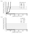
- Fig. 5 is a graph depicting the result of carrying out thermal shock tests on the wiring substrate 1 according to Embodiment 1.
- the vertical axis represents a resistance change rate (%) of the wiring substrate 1
- the horizontal axis represents the number of heat cycles in the thermal shock tests.
- the intrusion amount of the interlayer connecting conductor 12A into the upper wiring pattern 11 is 0 ⁇ m or 5 ⁇ m
- the resistance change rate increases as the number of heat cycles increases.
- the intrusion amount of the interlayer connecting conductor 12A into the upper wiring pattern 11 is 10 ⁇ m, 15 ⁇ m or 20 ⁇ m
- the resistance change rate hardly changes regardless of the number of heat cycles.
- the intrusion amount is preferably not less than 10 ⁇ m for the reason that connection reliability degrades at a smaller value of the intrusion amount.
- the intrusion amount is preferably set to be not less than 10 ⁇ m regardless of the diameter of the interlayer connecting conductor 12A and the thickness of the upper wiring pattern 11.
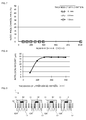
- Fig. 6 is a graph depicting the relationship between the diameter of the interlayer connecting conductor 12A and the connection reliability at the intrusion amount of 10 ⁇ m.
- Fig. 7 is a graph depicting the relationship between the thickness of the upper wiring pattern 11 and the connection reliability at the intrusion amount of 10 ⁇ m.
- connection reliability increases at the intrusion amount of not less than 10 ⁇ m resides in that the joining interface between the upper wiring pattern 11 and the interlayer connecting conductor 12A is not coplanar with the joining interface between the insulating layer 10 and the upper wiring pattern 11, which are different in thermal expansion coefficient from each other. Accordingly, the above-mentioned advantageous effect can be obtained regardless of the diameter of the interlayer connecting conductor 12A and the thickness of the upper wiring pattern 11.
- the resistance change rate hardly changes regardless of the number of heat cycles.
- the thickness of the upper wiring pattern 11 is any of 0.1 mm, 0.3 mm and 1.0 mm, the resistance change rate hardly changes regardless of the number of heat cycles.
- the thickness of the upper wiring pattern 11 is preferably set to be not less than 100 ⁇ m on that condition.
- Fig. 8 is a graph depicting the relationship between the upper wiring pattern 11 and the intrusion amount.
- the vertical axis represents the intrusion amount
- the horizontal axis represents the thickness of the upper wiring pattern 11.
- the intrusion amount is 10 ⁇ m
- the thickness of the upper wiring pattern 11 is about 100 ⁇ m.
- the intrusion amount is held substantially constant.
- the intrusion amount can be obtained as an optimum value of not less than 10 ⁇ m when the thickness of the upper wiring pattern 11 is not less than 100 ⁇ m.
- a wiring substrate according to Embodiment 2 will be described below.
- the wiring substrate 1 according to Embodiment 2 differs from that according to Embodiment 1 in making the interlayer connecting conductor 12A and the upper wiring pattern 11 electrically connected through a conductive adhesive. Only different point will be described below.
- Fig. 9 is a schematic sectional view of the wiring substrate 1 according to Embodiment 2.
- a conductive adhesive 13 is coated on the distal end portion of the interlayer connecting conductor 12A.
- the conductive adhesive 13 is, for example, a low-resistance conductive paste made of nano-silver or nano-copper. It is to be noted that the conductive adhesive 13 may be made of a resin composition containing metal powder.
- the conductive adhesive 13 is coated on the distal end portion of the interlayer connecting conductor 12A, the upper wiring pattern 11 and the interlayer connecting conductor 12A are electrically connected to each other through the conductive adhesive 13. With the presence of the conductive adhesive 13 coated on the interlayer connecting conductor 12A, the connection reliability of the interlayer connecting conductor 12A can be further increased.
- a method of manufacturing the wiring substrate 1 according to Embodiment 2 is substantially the same as that in Embodiment 1.
- the wiring substrate 1 according to Embodiment 2 can be manufactured by coating the conductive adhesive 13 on the distal end portion of the interlayer connecting conductor 12A in the third step illustrated in Fig. 4(c) .
- the intrusion amount is set to be not less than 10 ⁇ m in Embodiment 1, the intrusion amount can be set to be not less than 5 ⁇ m in the case where the conductive adhesive 13 is coated.
- Fig. 10 is a graph depicting the result of carrying out thermal shock tests on the wiring substrate 1 according to Embodiment 2. As seen from Fig. 10 , when the intrusion amount is not less than 5 ⁇ m, the resistance change rate hardly changes regardless of the number of heat cycles. Thus, the intrusion amount is preferably not less than 5 ⁇ m in Embodiment 2 for the reason that the connection reliability degrades at a smaller value of the intrusion amount.
- a wiring substrate according to Embodiment 3 will be described below.
- the wiring substrate 1 according to Embodiment 3 is different from that according to Embodiment 1 in that the insulating layer 10 has a multilayered structure, and a wiring pattern is formed between the adjacent layers. Only those different points will be described below.
- Fig. 11 is a schematic sectional view of the wiring substrate 1 according to Embodiment 3.
- the insulating layer 10 of the wiring substrate 1 according to Embodiment 3 is constituted as a laminate including a first layer 101, a second layer 102, a third layer 103, and a fourth layer 104, which are successively positioned in the mentioned order from the surface side of the insulating layer 10.
- the upper wiring pattern 11 is formed at an upper surface of the first layer 101, and a lower wiring pattern 121 is formed at a lower surface of the first layer 101.
- An interlayer connecting conductor 121A is formed integrally with the lower wiring pattern 121. A distal end portion of the interlayer connecting conductor 121A projects toward the upper wiring pattern 11 from the first layer 101 such that the distal end portion thereof intrudes into the upper wiring pattern 11.
- a lower wiring pattern 122 is formed at a lower surface of the second layer 102.
- An interlayer connecting conductor 122A is formed integrally with the lower wiring pattern 122.
- a distal end portion of the interlayer connecting conductor 122A projects toward the lower wiring pattern 121 from the second layer 102 such that the distal end portion of the interlayer connecting conductor 122A intrudes into the lower wiring pattern 121.
- a lower wiring pattern 123 is formed at a lower surface of the third layer 103.
- An interlayer connecting conductor 123A is formed integrally with the lower wiring pattern 123.
- a distal end portion of the interlayer connecting conductor 123A projects toward the lower wiring pattern 122 from the third layer 103 such that the distal end portion of the interlayer connecting conductor 123A intrudes into the lower wiring pattern 122.
- a lower wiring pattern 124 is formed at a lower surface of the fourth layer 104.
- An interlayer connecting conductor 124A is formed integrally with the lower wiring pattern 124.
- a distal end portion of the interlayer connecting conductor 124A projects toward the lower wiring pattern 123 from the fourth layer 104 such that the distal end portion of the interlayer connecting conductor 124A intrudes into the lower wiring pattern 123.
- the wiring patterns have such a multilayered structure that, looking at the wiring pattern of each layer, the distal end portion of the interlayer connecting conductor formed integrally with the wiring pattern in the underlying layer is buried in the relevant wiring pattern. Therefore, as in Embodiment 1, it is possible to avoid peeling-off between the laminated layers, which may occur by stress generated due to a difference in expansion coefficient, and to prevent the occurrence of a conduction failure, cracking, etc.
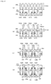
- Fig. 12 successively illustrates a series of manufacturing steps of the wiring substrate 1 according to Embodiment 3.
- a copper plate 204 is etched to form the interlayer connecting conductors 124A, and an insulating resin 234 is laminated on the copper plate 204 such that the distal end portion of each interlayer connecting conductor 124A projects out from the insulating resin 234 by 0.05 mm.
- the insulating resin 234 becomes the fourth layer 104 in Fig. 11 .
- a copper plate 203 having a thickness of 0.3 mm is placed on an upper surface of the insulating resin 234, and they are subjected to lamination molding for 1 hour at 180°C and 100 kN. As a result, the distal end portion of the interlayer connecting conductor 124A is caused to intrude into the copper plate 203.
- a dry film resist (not illustrated) having a thickness of 15 ⁇ m is pasted to an upper surface of the copper plate 203.
- the copper plate 203 is then etched such that the cylindrical interlayer connecting conductors 123A, each having the diameter of 0.6 mm and the length of 0.2 mm, remain on the upper surface side of the copper plate 203.
- holes (not illustrated), each having a diameter of 0.6 mm, are formed in an insulating resin 233 having a thickness of 0.15 mm, and the insulating resin 233 is laminated on the fourth layer 104 such that the interlayer connecting conductors 123A formed in Fig. 12(c) are inserted to the holes, respectively.
- the insulating resin 233 becomes the third layer 103 in Fig. 11 .
- the wiring substrate 1 according to Embodiment 3, illustrated in Fig. 11 can be formed by successively repeating the steps described above with reference to Fig. 12 .
- the size of the wiring substrate 1 can be further reduced by forming the wiring patterns inside the insulating layer 10 in the multilayered structure.
- a wiring substrate according to Embodiment 4 will be described below.
- the wiring substrate 1 according to Embodiment 4 is different from that according to Embodiment 3 in mounting electronic components inside the insulating layer 10 of the wiring substrate 1 according to Embodiment 3. Only such a different point will be described below.
- Fig. 13 is a schematic sectional view of the wiring substrate 1 according to Embodiment 4.
- the insulating layer 10 of the wiring substrate 1 according to Embodiment 4 is constituted as a laminate including the first layer 101, the second layer 102, the third layer 103, and the fourth layer 104, which are successively positioned in the mentioned order from the surface side of the insulating layer 10.
- lands 121B, 122B, 123B and 124B are formed integrally with the lower wiring patterns 121, 122, 123 and 124 that are formed at lower surfaces of the first layer 101, the second layer 102, the third layer 103, and the fourth layer 104, respectively.
- Electronic components 151, 152, 153 and 154 are mounted respectively to the lands 121B, 122B, 123B and 124B in the individual layers.
- the electronic components 151, 152, 153 and 154 are disposed respectively in the first layer 101, the second layer 102, the third layer 103, and the fourth layer 104.
- the size of the wiring substrate 1 can be reduced.
- the electronic components 151, 152, 153 and 154 are, for example, active elements such as silicon semiconductor elements or gallium arsenide semiconductor elements, or passive elements such as capacitors or inductors.
- Fig. 14 successively illustrates a series of manufacturing steps for the wiring substrate 1 according to Embodiment 4.
- a first step ( Fig. 14(a) ), dry film resists (not illustrated) each having a thickness of 15 ⁇ m are pasted to both surfaces of a copper plate 20 having a thickness of 0.3 mm, which surfaces are opposed to each other in the direction of thickness of the copper plate.
- the copper plate 204 including the dry film resists pasted thereto is etched from one surface side such that the cylindrical interlayer connecting conductors 124A, each having the diameter of 0.6 mm and the length of 0.19 mm, remain on the one surface side.
- a second step ( Fig. 14(b) ), the copper plate 204 having been subjected to the etching in Fig. 14(a) is further etched to form lands 124B each having a thickness of 0.01 mm.
- the interlayer connecting conductor 124A having been formed in the length of 0.19 mm is caused to have the length of 0.2 mm.
- a third step ( Fig. 14(c) ) the electronic component 154 is mounted to the formed lands 124B.
- an insulating resin 234 is laminated on the copper plate 204.
- the insulating resin 234 is in a liquid phase.
- the insulating resin 234 is subjected to debubbling under vacuum and then heated to such an extent that the insulating resin 234 in a semi-hardened state encapsulates the electronic component 154. At that time, the insulating resin 234 has a thickness of 0.15 mm.
- a copper plate 203 having a thickness of 0.3 mm is placed on the insulating resin 234, and they are subjected to lamination molding for 1 hour at 180°C and 100 kN.
- the wiring substrate 1 illustrated in Fig. 13 is formed by subsequently repeating the above-described steps from the step illustrated in Fig. 14(a) .
- the size of the wiring substrate 1 can be reduced.
Landscapes
- Engineering & Computer Science (AREA)
- Microelectronics & Electronic Packaging (AREA)
- Manufacturing & Machinery (AREA)
- Production Of Multi-Layered Print Wiring Board (AREA)
- Printing Elements For Providing Electric Connections Between Printed Circuits (AREA)
Abstract
Description
- The present invention relates to a wiring substrate in which a conductor pattern is formed in an insulating layer.
- In a wiring substrate, an interlayer connecting conductor (via hole conductor) for electrically connecting wiring patterns in different layers to each other is generally formed by boring a through-hole in the wiring substrate and coating a plating over an inner wall of the through-hole. However, such a method has problems from the viewpoint of productivity, economic efficiency, and so on because chemicals used in the plating process is expensive and the processing time is relatively long.
- To cope with the above-mentioned problems, there is proposed, for example, a method of forming an interlayer connecting conductor by filling a conductive paste, which contains metal powder, into a through-hole formed in an insulating layer of a wiring substrate. In the proposed method, after forming the interlayer connecting conductor by filling the conductive paste into the through-hole, the interlayer connecting conductor is compacted by pressing a wiring circuit layer made of a metal foil against the interlayer connecting conductor. At that time, there is a risk that, with the pressing of the wiring circuit layer, the conductor paste in the interlayer connecting conductor may spread out into a gap between the insulating layer and the wiring circuit layer, and adhesion between the insulating layer and the wiring circuit layer may lower, thus causing a conduction failure in the wiring substrate.
-
Patent Document 1 discloses a wiring substrate having features to prevent the conductor paste of the interlayer connecting conductor from spreading out to the surroundings of the interlayer connecting conductor, and to avoid an adhesion failure from occurring between the wiring circuit layer and the insulating layer.Fig. 1 is a schematic sectional view of the wiring substrate disclosed inPatent Document 1. In the wiring substrate illustrated inFig. 1 ,insulating layers 501A and 501B, each containing a thermosetting resin, are laminated, and awiring circuit layer 502 is buried in the surface of each insulating layer. - Through-holes for connecting the
wiring circuit layers 502 to each other are formed in theinsulating layers 501A and 501B. Aninterlayer connecting conductor 503 is formed in each through-hole by filling a conductor material, which contains metal powder, into the through-hole. Furthermore, thewiring circuit layer 502 has arecess 504 into which theinterlayer connecting conductor 503 intrudes to be buried therein. Therecess 504 serves to prevent the conductor paste of theinterlayer connecting conductor 503 from spreading out to the surroundings of theinterlayer connecting conductor 503. -
- Patent Document 1: Japanese Unexamined Patent Application Publication No.
2003-8225 -
Patent Document 1 accompanies with a risk that, if therecess 504 formed in thewiring circuit layers 502 is too shallow, the effect of preventing the spreading-out of the conductor paste would be reduced, and if it is too deep, the thickness of thewiring circuit layers 502 would be reduced and the strength of thewiring circuit layers 502 would be reduced. In other words,Patent Document 1 accompanies with a risk that connection reliability in the wiring substrate may degrade because the adhesion failure between the wiring circuit layers and the insulating layer cannot be sufficiently avoided. - Moreover, in
Patent Document 1, the interlayer connecting conductor is formed by filling the conductor paste into the through-hole. However, because the conductor paste is made of the resin containing the metal powder, an amount of metal component in the interlayer connecting conductor is relatively small. As a result, a resistance value of the interlayer connecting conductor increases. This raises another problem that the interlayer connecting conductor impedes flow of a current, thus making the wiring substrate not adaptable for a large current. - Accordingly, an object of the present invention is to provide a wiring substrate that is adaptable for a large current without causing degradation of reliability in connection, which may occur by cracking, disconnection, interlayer peeling-off, etc.
- The present invention provides a wiring substrate comprising an insulating layer, a first conductive pattern and a second conductive pattern disposed in sandwiching relation to the insulating layer, and an interlayer connecting conductor penetrating through the insulating layer in a direction of thickness thereof and electrically connecting the first conductive pattern and the second conductive pattern to each other, wherein the interlayer connecting conductor is formed integrally with the first conductive pattern, and the interlayer connecting conductor is joined to the second conductive pattern in a state intruding into the second conductive pattern beyond a joining interface between the insulating layer and the second conductive pattern.
- With the features described above, the interlayer connecting conductor electrically connecting the first conductive pattern and the second conductive pattern to each other is formed integrally with the first conductive pattern, and the interlayer connecting conductor is in a state intruding into the second conductive pattern. In other words, a joining interface between the interlayer connecting conductor and the second conductive pattern is not coplanar with the joining interface between the insulating layer and the second conductive pattern. Here, the expression "formed integrally" implies that the interlayer connecting conductor and the first conductive pattern are formed of a single integral metal member, and there is no joining interface therebetween.
- With expansion and contraction depending on temperature changes (overheating and cooling), stress generates in a joining portion between the insulating layer and the conductive pattern due to a difference in expansion coefficient therebetween. If the joining interface between the interlayer connecting conductor and the second conductive pattern is coplanar with the joining interface between the insulating layer and the second conductive pattern, there is a risk that the generated stress may concentrate at the joining interface and peeling-off may occur at the joining interface. This result in a possibility of causing a conduction failure between the first conductive pattern and the second conductive pattern, or generating cracks in the wiring substrate.
- To cope with the above-mentioned problems, the interlayer connecting conductor is caused to intrude into the second conductive pattern such that the joining interface between the interlayer connecting conductor and the second conductive pattern and the joining interface between the insulating layer and the second conductive pattern are positioned in different planes. With such an arrangement, the generated stress can be distributed. It is hence possible to prevent the conduction failure caused by the peeling-off or the cracks generated in the wiring substrate.
- Furthermore, when conductive patterns in different layers are connected to each other, as in the related art, by an interlayer connecting conductor that is formed by filling metal powder into a through-hole, a resistance value in a connecting portion between the conductive pattern and the interlayer connecting conductor increases because they are made of different materials. In contrast, according to the present invention, since a connecting conductor serving as the interlayer connecting conductor is formed integrally with the first conductive pattern, a resistance value in a connecting portion between the first conductive pattern and the interlayer connecting conductor can be prevented from increasing, and the above-mentioned problem with the related art can be avoided.
- Moreover, since the interlayer connecting conductor and the second conductive pattern are formed integrally with each other unlike the related-art using the method of filling the conductive paste, an amount of metal component contained in the interlayer connecting conductor can be increased, whereby a resistance value of the interlayer connecting conductor can be reduced.
- In the wiring substrate according to the present invention, the insulating layer may be made up of plural layers, and the conductive pattern may be formed on a surface of an uppermost one of the plural layers constituting the insulating layer.
- With the features described above, a conduction failure can be prevented in the surface of the uppermost one of the plural insulating layers to which an electronic component is generally mounted.
- In the wiring substrate according to the present invention, preferably, the interlayer connecting conductor and the second conductive pattern are electrically connected to each other in at least parts thereof through a conductive adhesive.
- With the feature described above, connection reliability between the interlayer connecting conductor and the second conductive pattern can be improved because they are electrically connected to each other through the conductive adhesive.
- In the wiring substrate according to the present invention, preferably, an organic coating is formed in at least part of a joining interface between the interlayer connecting conductor and the second conductive pattern.
- With the feature described above, since oxidation in a connecting portion between the interlayer connecting conductor and the second conductive pattern can be suppressed, a resistance value in that connecting portion can be avoided from increasing.
- In the wiring substrate according to the present invention, preferably, at least the interlayer connecting conductor is subjected to surface treatment. The surface treatment is, for example, roughing, blackening, coupling, and formation of an organic coating.
- With the feature described above, since the interlayer connecting conductor is subjected to the surface treatment, adhesion between the insulating resin and the interlayer connecting conductor increases, and peeling-off can be suppressed which may occur by stress generated due to a difference in expansion coefficient between two adjacent members. It is hence possible to prevent a conduction failure caused by the peeling-off, cracks generated in the wiring substrate, etc. The peeling-off occurred between the insulating resin and the interlayer connecting conductor leads to the conduction failure with a high probability. Thus, the surface of the interlayer connecting conductor is an essential region where the surface treatment is to be performed. In addition to the surface of the interlayer connecting conductor, the surface of the first conductive pattern and the surface of the second conductive pattern may also be subjected to the surface treatment.
- In the wiring substrate according to the present invention, the first conductive pattern may have lands formed integrally therewith on side close to the insulating layer, and the wiring substrate may further comprise an electronic component mounted to the lands and disposed inside the insulating layer.
- With the features described above, since the electronic component can be incorporated inside the insulating layer, the size of the wiring substrate can be reduced.
- In the wiring substrate according to the present invention, preferably, the interlayer connecting conductor intrudes into the second conductive pattern by 10 µm or more at a most deeply intruding portion thereof.
- With the feature described above, since an amount by which the interlayer connecting conductor intrudes into the second conductive pattern at the most deeply intruding portion thereof is set to be 10 µm or more, the occurrence of a failure due to the peeling-off between the interlayer connecting conductor and the second conductive pattern can be suppressed, and the connection reliability in the wiring substrate can be increased.
- According to the present invention, since the joining interface between the interlayer connecting conductor and the second conductive pattern and the joining interface between the second conductive pattern and the insulating layer are positioned in different planes, stress generated due to a difference in expansion coefficient between two adjacent members can be distributed. It is hence possible to prevent the interlayer peeling-off and the conduction failure attributable to the stress, and to increase the connection reliability in the wiring substrate. In addition, since the interlayer connecting conductor is formed integrally with the first conductive pattern, an amount of metal component contained in the interlayer connecting conductor can be increased, whereby a resistance value of the interlayer connecting conductor can be reduced. Brief Description of Drawings
-
- [
Fig. 1] Fig. 1 is a schematic sectional view of a wiring substrate described inPatent Document 1. - [
Fig. 2] Fig. 2 is a schematic sectional view of a wiring substrate according toEmbodiment 1. - [
Fig. 3] Fig. 3 illustrates, in enlarged scale, a circular portion surrounded by a one-dot-chain line inFig. 2 . - [
Fig. 4] Fig. 4 successively illustrates a series of manufacturing steps for the wiring substrate according toEmbodiment 1. - [
Fig. 5] Fig. 5 is a graph depicting the result of carrying out thermal shock tests on the wiring substrate according toEmbodiment 1. - [
Fig. 6] Fig. 6 is a graph depicting the relationship between the diameter of an interlayer connecting conductor and connection reliability at an intrusion amount of 10 µm. - [
Fig. 7] Fig. 7 is a graph depicting the relationship between the thickness of an upper wiring pattern and connection reliability at the intrusion amount of 10 µm. - [
Fig. 8] Fig. 8 is a graph depicting the relationship between the upper wiring pattern and the intrusion amount. - [
Fig. 9] Fig. 9 is a schematic sectional view of a wiring substrate according toEmbodiment 2. - [
Fig. 10] Fig. 10 is a graph depicting the result of carrying out thermal shock tests on the wiring substrate according toEmbodiment 2. - [
Fig. 11] Fig. 11 is a schematic sectional view of a wiring substrate according toEmbodiment 3. - [
Fig. 12] Fig. 12 successively illustrates a series of manufacturing steps for the wiring substrate according toEmbodiment 3. - [
Fig. 13] Fig. 13 is a schematic sectional view of a wiring substrate according toEmbodiment 4. - [
Fig. 14] Fig. 14 successively illustrates a series of manufacturing steps for the wiring substrate according toEmbodiment 4. - The wiring substrate according to the present invention includes an insulating layer made of an insulating resin, and a conductive wiring pattern (conductive pattern) disposed on the insulating layer. The insulating layer may be a single layer or made up of plural layers. The insulating resin forming the insulating layer is, for example, a glass epoxy resin, an epoxy resin, a phenol resin, a cyanate resin, or a polyimide resin. Among those examples, the polyimide resin is particularly preferable in exhibiting superior heat resistance after being hardened.
- The wiring substrate electrically connects, through the wiring pattern, an electronic component mounted to the surface of the insulating layer and a main substrate (e.g., a mother board) to which the wiring substrate is mounted. The electronic component mounted to the wiring substrate is, for example, an active element such as a silicon semiconductor element or a gallium arsenide semiconductor element, or a passive element such as a capacitor or an inductor.
-
Fig. 2 is a schematic sectional view of a wiring substrate according toEmbodiment 1.Fig. 3 illustrates, in enlarged scale, a circular portion surrounded by a one-dot-chain line inFig. 2 . It is to be noted that, inFig. 3 , though individual members are actually in a state of being closely contacted with each other, the members are drawn with gaps left at joining boundaries between them for convenience of explanation. - In a
wiring substrate 1 according toEmbodiment 1, anupper wiring pattern 11 is formed at an upper surface of an insulatinglayer 10, and alower wiring pattern 12 is formed at a lower surface of the insulatinglayer 10. The upper surface of the insulatinglayer 10 serves as the above-mentioned surface to which the electronic component is mounted. - The insulating
layer 10 has a thickness of 0.10 mm and includes a cylindrical through-via 10A formed therein. Aninterlayer connecting conductor 12A formed integrally with thelower wiring pattern 12, as described below, is inserted to the through-via 10A. Theupper wiring pattern 11 and thelower wiring pattern 12 formed respectively at the upper and lower surfaces of the insulatinglayer 10 are electrically connected to each other by theinterlayer connecting conductor 12A. - The
wiring pattern 11 is formed at the upper surface of the insulatinglayer 10 and has a thickness of 0.10 mm. A distal end portion of the later-describedinterlayer connecting conductor 12A, projecting out from the insulatinglayer 10, intrudes into theupper wiring pattern 11 at each position that is aligned with the through-via 10A formed in the insulatinglayer 10 when viewed in the direction of thickness thereof. While a joininginterface 11A between theupper wiring pattern 11 and theinterlayer connecting conductor 12A has a circular arc shape in section as illustrated inFig. 3 , the joininginterface 11A may have a rectangular shape. - The
lower wiring pattern 12 is formed at the lower surface of the insulatinglayer 10 and has a thickness of 0.10 mm. Theinterlayer connecting conductor 12A is formed integrally with thelower wiring pattern 12. In other words, thelower wiring pattern 12 and theinterlayer connecting conductor 12A are formed of a single integral metal member, and there is no joining interface therebetween. - The
interlayer connecting conductor 12A has a cylindrical shape with a diameter of 0.6 mm and a length of 0.2 mm. As illustrated inFig. 3 , the distal end portion of theinterlayer connecting conductor 12A has a circular arc shape. Theinterlayer connecting conductor 12A is inserted to the through-via 10A formed in the insulatinglayer 10. Thus, the distal end portion of theinterlayer connecting conductor 12A projecting out from the upper surface of the insulatinglayer 10 is burred in theupper wiring pattern 11. - By forming the
lower wiring pattern 12 and theinterlayer connecting conductor 12A integrally with each other, an amount of metal component contained therein can be increased and a resistance value of the interlayer connecting conductor can be reduced in comparison with the case where the interlayer connecting conductor is formed by filling the conductor paste, which is made of the resin containing the metal powder, into the through-hole. - While the
interlayer connecting conductor 12A has the cylindrical shape in this embodiment, it may have a rectangular columnar shape. Furthermore, the distal end portion of theinterlayer connecting conductor 12A may have a planar shape. - Thus, since the
upper wiring pattern 11 is buried in theinterlayer connecting conductor 12A, a joining interface between theinterlayer connecting conductor 12A and theupper wiring pattern 11 is positioned in a plane different from a joining interface between the insulatinglayer 10 and theupper wiring pattern 11. It is therefore possible to avoid stress generated due to a difference in expansion coefficient from concentrating at the joining interface, and to prevent a conduction failure caused by peeling-off attributable to the stress, cracks generated in thewiring substrate 1, etc. - A method of manufacturing the
wiring substrate 1 will be described below.Fig. 4 successively illustrates a series of manufacturing steps for the wiring substrate according toEmbodiment 1. - In a first step (
Fig. 4(a) ), dry film resists 21 each having a thickness of 15 µm are pasted to both surfaces of acopper plate 20 having a thickness of 0.3 mm, which surfaces are opposed to each other in the direction of thickness of the copper plate. It is to be noted thatFig. 4 illustrates thecopper plate 20 when viewed from a side. - Next, in a second step (
Fig. 4(b) ), thecopper plate 20 including the dry film resists 21 pasted thereto is etched from one surface side such that the cylindricalinterlayer connecting conductors 12A, each having the diameter of 0.6 mm and the length of 0.2 mm, remain on the one surface side. - In a third step (
Fig. 4(c) ), holes (not illustrated), each having a diameter of 0.6 mm, are formed in an insulatingresin 23 having a thickness of 0.15 mm, and the insulatingresin 23 is laminated on thecopper plate 20 that has been subjected to the etching in the second step. The insulatingresin 23 becomes the insulatinglayer 10. - In a fourth step (
Fig. 4(d) ), acopper plate 24 having a thickness of 0.1 mm is placed on an upper surface of the insulating resin 23 (i.e., the insulating layer 10). In such a state, they are subjected to lamination molding for 1 hour at 180°C and 100 kN. As a result, the distal end portion of theinterlayer connecting conductor 12A is caused to intrude into thecopper plate 24, and the above-mentioned joininginterface 11A is formed in a circular arc shape. - In a fifth step (
Fig. 4(e) ), patterns are formed on both surfaces of a laminate, obtained in the fourth step, by a subtractive process (i.e., a process of removing unnecessary portions while leaving a circuit). As a result, thecopper plate 20 is formed into thelower wiring pattern 12, and thecopper plate 24 is formed into theupper wiring pattern 11. Thewiring substrate 1 is thus completed. - An intrusion amount by which the
interlayer connecting conductor 12A is buried in theupper wiring pattern 11 will be described below. The intrusion amount is preferably set to be not more than 50% of the thickness of theupper wiring pattern 11. That point will be described in more detail below in connection with practical values. -
Fig. 5 is a graph depicting the result of carrying out thermal shock tests on thewiring substrate 1 according toEmbodiment 1. In the graph ofFig. 5 , the vertical axis represents a resistance change rate (%) of thewiring substrate 1, and the horizontal axis represents the number of heat cycles in the thermal shock tests. - As seen from
Fig. 5 , when the intrusion amount of theinterlayer connecting conductor 12A into theupper wiring pattern 11 is 0 µm or 5 µm, the resistance change rate increases as the number of heat cycles increases. On the other hand, when the intrusion amount of theinterlayer connecting conductor 12A into theupper wiring pattern 11 is 10 µm, 15 µm or 20 µm, the resistance change rate hardly changes regardless of the number of heat cycles. Thus, the intrusion amount is preferably not less than 10 µm for the reason that connection reliability degrades at a smaller value of the intrusion amount. - Moreover, the intrusion amount is preferably set to be not less than 10 µm regardless of the diameter of the
interlayer connecting conductor 12A and the thickness of theupper wiring pattern 11.Fig. 6 is a graph depicting the relationship between the diameter of theinterlayer connecting conductor 12A and the connection reliability at the intrusion amount of 10 µm.Fig. 7 is a graph depicting the relationship between the thickness of theupper wiring pattern 11 and the connection reliability at the intrusion amount of 10 µm. - The reason why the connection reliability increases at the intrusion amount of not less than 10 µm resides in that the joining interface between the
upper wiring pattern 11 and theinterlayer connecting conductor 12A is not coplanar with the joining interface between the insulatinglayer 10 and theupper wiring pattern 11, which are different in thermal expansion coefficient from each other. Accordingly, the above-mentioned advantageous effect can be obtained regardless of the diameter of theinterlayer connecting conductor 12A and the thickness of theupper wiring pattern 11. - For example, as seen from
Fig. 6 , when the diameter of theinterlayer connecting conductor 12A is any of 0.05 mm, 0.6 mm and 1.0 mm, the resistance change rate hardly changes regardless of the number of heat cycles. Furthermore, as seen fromFig. 7 , when the thickness of theupper wiring pattern 11 is any of 0.1 mm, 0.3 mm and 1.0 mm, the resistance change rate hardly changes regardless of the number of heat cycles. - While the intrusion amount is preferably not less than 10 µm, the thickness of the
upper wiring pattern 11 is preferably set to be not less than 100 µm on that condition.Fig. 8 is a graph depicting the relationship between theupper wiring pattern 11 and the intrusion amount. In the graph ofFig. 8 , the vertical axis represents the intrusion amount, and the horizontal axis represents the thickness of theupper wiring pattern 11. As seen fromFig. 8 , when the intrusion amount is 10 µm, the thickness of theupper wiring pattern 11 is about 100 µm. When the thickness of theupper wiring pattern 11 is not less than 100 µm, the intrusion amount is held substantially constant. Thus, the intrusion amount can be obtained as an optimum value of not less than 10 µm when the thickness of theupper wiring pattern 11 is not less than 100 µm. - A wiring substrate according to
Embodiment 2 will be described below. Thewiring substrate 1 according toEmbodiment 2 differs from that according toEmbodiment 1 in making theinterlayer connecting conductor 12A and theupper wiring pattern 11 electrically connected through a conductive adhesive. Only different point will be described below. -
Fig. 9 is a schematic sectional view of thewiring substrate 1 according toEmbodiment 2. In thewiring substrate 1 according toEmbodiment 2, as illustrated inFig. 9 , aconductive adhesive 13 is coated on the distal end portion of theinterlayer connecting conductor 12A. Theconductive adhesive 13 is, for example, a low-resistance conductive paste made of nano-silver or nano-copper. It is to be noted that theconductive adhesive 13 may be made of a resin composition containing metal powder. - Since the
conductive adhesive 13 is coated on the distal end portion of theinterlayer connecting conductor 12A, theupper wiring pattern 11 and theinterlayer connecting conductor 12A are electrically connected to each other through theconductive adhesive 13. With the presence of the conductive adhesive 13 coated on theinterlayer connecting conductor 12A, the connection reliability of theinterlayer connecting conductor 12A can be further increased. - A method of manufacturing the
wiring substrate 1 according toEmbodiment 2 is substantially the same as that inEmbodiment 1. Thewiring substrate 1 according toEmbodiment 2 can be manufactured by coating the conductive adhesive 13 on the distal end portion of theinterlayer connecting conductor 12A in the third step illustrated inFig. 4(c) . - While the intrusion amount is set to be not less than 10 µm in
Embodiment 1, the intrusion amount can be set to be not less than 5 µm in the case where theconductive adhesive 13 is coated.Fig. 10 is a graph depicting the result of carrying out thermal shock tests on thewiring substrate 1 according toEmbodiment 2. As seen fromFig. 10 , when the intrusion amount is not less than 5 µm, the resistance change rate hardly changes regardless of the number of heat cycles. Thus, the intrusion amount is preferably not less than 5 µm inEmbodiment 2 for the reason that the connection reliability degrades at a smaller value of the intrusion amount. - A wiring substrate according to
Embodiment 3 will be described below. Thewiring substrate 1 according toEmbodiment 3 is different from that according toEmbodiment 1 in that the insulatinglayer 10 has a multilayered structure, and a wiring pattern is formed between the adjacent layers. Only those different points will be described below. -
Fig. 11 is a schematic sectional view of thewiring substrate 1 according toEmbodiment 3. As illustrated inFig. 11 , the insulatinglayer 10 of thewiring substrate 1 according toEmbodiment 3 is constituted as a laminate including afirst layer 101, asecond layer 102, athird layer 103, and afourth layer 104, which are successively positioned in the mentioned order from the surface side of the insulatinglayer 10. - The
upper wiring pattern 11 is formed at an upper surface of thefirst layer 101, and alower wiring pattern 121 is formed at a lower surface of thefirst layer 101. Aninterlayer connecting conductor 121A is formed integrally with thelower wiring pattern 121. A distal end portion of theinterlayer connecting conductor 121A projects toward theupper wiring pattern 11 from thefirst layer 101 such that the distal end portion thereof intrudes into theupper wiring pattern 11. - A
lower wiring pattern 122 is formed at a lower surface of thesecond layer 102. Aninterlayer connecting conductor 122A is formed integrally with thelower wiring pattern 122. A distal end portion of theinterlayer connecting conductor 122A projects toward thelower wiring pattern 121 from thesecond layer 102 such that the distal end portion of theinterlayer connecting conductor 122A intrudes into thelower wiring pattern 121. - A
lower wiring pattern 123 is formed at a lower surface of thethird layer 103. Aninterlayer connecting conductor 123A is formed integrally with thelower wiring pattern 123. A distal end portion of theinterlayer connecting conductor 123A projects toward thelower wiring pattern 122 from thethird layer 103 such that the distal end portion of theinterlayer connecting conductor 123A intrudes into thelower wiring pattern 122. - A
lower wiring pattern 124 is formed at a lower surface of thefourth layer 104. Aninterlayer connecting conductor 124A is formed integrally with thelower wiring pattern 124. A distal end portion of theinterlayer connecting conductor 124A projects toward thelower wiring pattern 123 from thefourth layer 104 such that the distal end portion of theinterlayer connecting conductor 124A intrudes into thelower wiring pattern 123. - In the
wiring substrate 1 according toEmbodiment 3, as described above, the wiring patterns have such a multilayered structure that, looking at the wiring pattern of each layer, the distal end portion of the interlayer connecting conductor formed integrally with the wiring pattern in the underlying layer is buried in the relevant wiring pattern. Therefore, as inEmbodiment 1, it is possible to avoid peeling-off between the laminated layers, which may occur by stress generated due to a difference in expansion coefficient, and to prevent the occurrence of a conduction failure, cracking, etc. -
Fig. 12 successively illustrates a series of manufacturing steps of thewiring substrate 1 according toEmbodiment 3. - As illustrated in
Fig. 12(a) , acopper plate 204 is etched to form theinterlayer connecting conductors 124A, and an insulatingresin 234 is laminated on thecopper plate 204 such that the distal end portion of eachinterlayer connecting conductor 124A projects out from the insulatingresin 234 by 0.05 mm. The insulatingresin 234 becomes thefourth layer 104 inFig. 11 . - A
copper plate 203 having a thickness of 0.3 mm is placed on an upper surface of the insulatingresin 234, and they are subjected to lamination molding for 1 hour at 180°C and 100 kN. As a result, the distal end portion of theinterlayer connecting conductor 124A is caused to intrude into thecopper plate 203. - Next, as illustrated in
Fig. 12(b) , a dry film resist (not illustrated) having a thickness of 15 µm is pasted to an upper surface of thecopper plate 203. Thecopper plate 203 is then etched such that the cylindricalinterlayer connecting conductors 123A, each having the diameter of 0.6 mm and the length of 0.2 mm, remain on the upper surface side of thecopper plate 203. - Next, as illustrated in
Fig. 12(c) , patterns are formed on both surfaces of a laminate, obtained as illustrated inFig. 12(b) , by the subtractive process. As a result, thecopper plate 204 is formed into thelower wiring pattern 124, and thecopper plate 203 is formed into thelower wiring pattern 123. - Next, as illustrated in
Fig. 12(d) , holes (not illustrated), each having a diameter of 0.6 mm, are formed in an insulatingresin 233 having a thickness of 0.15 mm, and the insulatingresin 233 is laminated on thefourth layer 104 such that theinterlayer connecting conductors 123A formed inFig. 12(c) are inserted to the holes, respectively. The insulatingresin 233 becomes thethird layer 103 inFig. 11 . - The
wiring substrate 1 according toEmbodiment 3, illustrated inFig. 11 , can be formed by successively repeating the steps described above with reference toFig. 12 . Thus, the size of thewiring substrate 1 can be further reduced by forming the wiring patterns inside the insulatinglayer 10 in the multilayered structure. - A wiring substrate according to
Embodiment 4 will be described below. Thewiring substrate 1 according toEmbodiment 4 is different from that according toEmbodiment 3 in mounting electronic components inside the insulatinglayer 10 of thewiring substrate 1 according toEmbodiment 3. Only such a different point will be described below. -
Fig. 13 is a schematic sectional view of thewiring substrate 1 according toEmbodiment 4. As inEmbodiment 3, the insulatinglayer 10 of thewiring substrate 1 according toEmbodiment 4 is constituted as a laminate including thefirst layer 101, thesecond layer 102, thethird layer 103, and thefourth layer 104, which are successively positioned in the mentioned order from the surface side of the insulatinglayer 10. - In addition to the
interlayer connecting conductors lower wiring patterns first layer 101, thesecond layer 102, thethird layer 103, and thefourth layer 104, respectively. -
Electronic components lands electronic components first layer 101, thesecond layer 102, thethird layer 103, and thefourth layer 104. Thus, with theelectronic components wiring substrate 1 can be reduced. - The
electronic components -
Fig. 14 successively illustrates a series of manufacturing steps for thewiring substrate 1 according toEmbodiment 4. - In a first step (
Fig. 14(a) ), dry film resists (not illustrated) each having a thickness of 15 µm are pasted to both surfaces of acopper plate 20 having a thickness of 0.3 mm, which surfaces are opposed to each other in the direction of thickness of the copper plate. Thecopper plate 204 including the dry film resists pasted thereto is etched from one surface side such that the cylindricalinterlayer connecting conductors 124A, each having the diameter of 0.6 mm and the length of 0.19 mm, remain on the one surface side. - In a second step (
Fig. 14(b) ), thecopper plate 204 having been subjected to the etching inFig. 14(a) is further etched to formlands 124B each having a thickness of 0.01 mm. With the step of forming thelands 124B, theinterlayer connecting conductor 124A having been formed in the length of 0.19 mm is caused to have the length of 0.2 mm. - In a third step (
Fig. 14(c) ), theelectronic component 154 is mounted to the formed lands 124B. Thereafter, in a fourth step (Fig. 14(d) ), an insulatingresin 234 is laminated on thecopper plate 204. InEmbodiment 4, the insulatingresin 234 is in a liquid phase. After coating the insulatingresin 234 over thecopper plate 204, the insulatingresin 234 is subjected to debubbling under vacuum and then heated to such an extent that the insulatingresin 234 in a semi-hardened state encapsulates theelectronic component 154. At that time, the insulatingresin 234 has a thickness of 0.15 mm. - Thereafter, as in the step (see
Fig. 12 ) described above inEmbodiment 3, acopper plate 203 having a thickness of 0.3 mm is placed on the insulatingresin 234, and they are subjected to lamination molding for 1 hour at 180°C and 100 kN. Thewiring substrate 1 illustrated inFig. 13 is formed by subsequently repeating the above-described steps from the step illustrated inFig. 14(a) . Thus, with the electronic components incorporated in the insulating resin, the size of thewiring substrate 1 can be reduced. - While the wiring substrate according to the present invention has been described in detail above, practical structures of the
wiring substrate 1 can be modified in design as required. The operations and the advantageous effects stated in the foregoing embodiments are merely explained as most preferable operations and advantageous effects obtained with the present invention. In other words, the operations and the advantageous effects of the present invention are not limited to those described above in the embodiments. -
- 1
- - wiring substrate
- 10
- - insulating layer
- 11
- - upper wiring pattern (second conductive pattern)
- 11A
- - joining interface
- 12
- - lower wiring pattern (first conductive pattern)
- 12A
- - interlayer connecting conductor
- 13
- - conductive adhesive
Claims (7)
- A wiring substrate comprising:an insulating layer;a first conductive pattern and a second conductive pattern disposed in sandwiching relation to the insulating layer; andan interlayer connecting conductor penetrating through the insulating layer in a direction of thickness thereof and electrically connecting the first conductive pattern and the second conductive pattern to each other,wherein the interlayer connecting conductor is formed integrally with the first conductive pattern, and the interlayer connecting conductor is joined to the second conductive pattern in a state intruding into the second conductive pattern beyond a joining interface between the insulating layer and the second conductive pattern.
- The wiring substrate according to Claim 1, wherein the insulating layer is made up of plural layers, and
the second conductive pattern is formed on a surface of an uppermost one of the plural layers constituting the insulating layer. - The wiring substrate according to Claim 1 or 2, wherein the interlayer connecting conductor and the second conductive pattern are electrically connected to each other in at least parts thereof through a conductive adhesive.
- The wiring substrate according to Claim 2 or 3, wherein the first conductive pattern has lands formed integrally therewith on side close to the insulating layer, and
the wiring substrate further comprises an electronic component mounted to the lands and disposed inside the insulating layer. - The wiring substrate according to any one of Claims 1 to 4, wherein the interlayer connecting conductor intrudes into the second conductive pattern by 10 µm or more at a most deeply intruding portion thereof.
- The wiring substrate according to any one of Claims 1 to 5, wherein an organic coating is formed in at least part of a joining interface between the interlayer connecting conductor and the second conductive pattern.
- The wiring substrate according to any one of Claims 1 to 6, wherein at least the interlayer connecting conductor is subjected to surface treatment.
Applications Claiming Priority (2)
| Application Number | Priority Date | Filing Date | Title |
|---|---|---|---|
| JP2011065226 | 2011-03-24 | ||
| PCT/JP2012/057120 WO2012128269A1 (en) | 2011-03-24 | 2012-03-21 | Wiring substrate |
Publications (2)
| Publication Number | Publication Date |
|---|---|
| EP2690941A1 true EP2690941A1 (en) | 2014-01-29 |
| EP2690941A4 EP2690941A4 (en) | 2014-09-03 |
Family
ID=46879414
Family Applications (1)
| Application Number | Title | Priority Date | Filing Date |
|---|---|---|---|
| EP12760032.8A Withdrawn EP2690941A4 (en) | 2011-03-24 | 2012-03-21 | WIRING SUBSTRATE |
Country Status (5)
| Country | Link |
|---|---|
| US (1) | US20140009899A1 (en) |
| EP (1) | EP2690941A4 (en) |
| JP (1) | JP5772949B2 (en) |
| CN (1) | CN103460819A (en) |
| WO (1) | WO2012128269A1 (en) |
Families Citing this family (6)
| Publication number | Priority date | Publication date | Assignee | Title |
|---|---|---|---|---|
| JP2014216599A (en) * | 2013-04-30 | 2014-11-17 | 株式会社村田製作所 | Wiring board and manufacturing method of the same |
| WO2014188964A1 (en) * | 2013-05-22 | 2014-11-27 | 株式会社村田製作所 | Component-embedded wiring board and manufacturing method for component-embedded wiring board |
| CN105097758B (en) | 2014-05-05 | 2018-10-26 | 日月光半导体制造股份有限公司 | Substrate, its semiconductor package and its manufacturing method |
| WO2016114400A1 (en) * | 2015-01-15 | 2016-07-21 | コニカミノルタ株式会社 | Laminated wiring structure, and methdod for forming laminated wiring structure |
| JP2019021876A (en) * | 2017-07-21 | 2019-02-07 | 日本特殊陶業株式会社 | Wiring board, planar transformer, and manufacturing method of wiring board |
| JP7299009B2 (en) * | 2018-10-18 | 2023-06-27 | 新光電気工業株式会社 | Multilayer substrate, electronic component, and method for manufacturing multilayer substrate |
Family Cites Families (19)
| Publication number | Priority date | Publication date | Assignee | Title |
|---|---|---|---|---|
| JPH0271590A (en) * | 1988-09-06 | 1990-03-12 | Mitsubishi Electric Corp | Substrate for hybrid ic |
| US6038133A (en) * | 1997-11-25 | 2000-03-14 | Matsushita Electric Industrial Co., Ltd. | Circuit component built-in module and method for producing the same |
| JP3348004B2 (en) * | 1998-01-29 | 2002-11-20 | 山一電機株式会社 | Multilayer wiring board and method of manufacturing the same |
| JP2000091746A (en) * | 1998-09-07 | 2000-03-31 | Toshiba Corp | Wiring board manufacturing method and wiring board |
| JP2001007533A (en) * | 1999-06-21 | 2001-01-12 | Mitsubishi Gas Chem Co Inc | Manufacture of ball grid array printed wiring board excellent in heat dissipating property |
| JP2001111189A (en) * | 1999-10-12 | 2001-04-20 | North:Kk | Wiring circuit board and manufacturing method thereof |
| JP2002124762A (en) * | 2000-10-16 | 2002-04-26 | Toshiba Chem Corp | Production method for multilayered printed wiring board |
| JP3769587B2 (en) * | 2000-11-01 | 2006-04-26 | 株式会社ノース | Wiring circuit member, manufacturing method thereof, multilayer wiring circuit board, and semiconductor integrated circuit device |
| JP2002151820A (en) * | 2000-11-07 | 2002-05-24 | Toshiba Chem Corp | Printed wiring board and its manufacturing method |
| JP2003008225A (en) | 2001-06-26 | 2003-01-10 | Kyocera Corp | Multilayer wiring board and method of manufacturing the same |
| JP4045143B2 (en) * | 2002-02-18 | 2008-02-13 | テセラ・インターコネクト・マテリアルズ,インコーポレイテッド | Manufacturing method of wiring film connecting member and manufacturing method of multilayer wiring board |
| JP3946114B2 (en) * | 2002-09-13 | 2007-07-18 | 日本メクトロン株式会社 | Manufacturing method of multilayer circuit wiring board |
| JP4185755B2 (en) * | 2002-10-31 | 2008-11-26 | テセラ・インターコネクト・マテリアルズ,インコーポレイテッド | Wiring board and manufacturing method thereof |
| US7190078B2 (en) * | 2004-12-27 | 2007-03-13 | Khandekar Viren V | Interlocking via for package via integrity |
| JP2008244029A (en) * | 2007-03-27 | 2008-10-09 | Ngk Spark Plug Co Ltd | Wiring board with built-in components, parts for wiring board |
| KR100811034B1 (en) * | 2007-04-30 | 2008-03-06 | 삼성전기주식회사 | Manufacturing Method of Printed Circuit Board with Electronic Device |
| JP2009158867A (en) * | 2007-12-27 | 2009-07-16 | Seiko Epson Corp | Multilayer substrate, semiconductor device and electronic device |
| JP2008153682A (en) * | 2008-01-24 | 2008-07-03 | Tadatomo Suga | Electronic component mounting apparatus and manufacturing method thereof |
| JP2011014728A (en) * | 2009-07-02 | 2011-01-20 | Casio Computer Co Ltd | Semiconductor device and method of manufacturing semiconductor device |
-
2012
- 2012-03-21 WO PCT/JP2012/057120 patent/WO2012128269A1/en not_active Ceased
- 2012-03-21 JP JP2013505976A patent/JP5772949B2/en not_active Expired - Fee Related
- 2012-03-21 EP EP12760032.8A patent/EP2690941A4/en not_active Withdrawn
- 2012-03-21 CN CN2012800146939A patent/CN103460819A/en active Pending
-
2013
- 2013-09-23 US US14/033,695 patent/US20140009899A1/en not_active Abandoned
Also Published As
| Publication number | Publication date |
|---|---|
| JPWO2012128269A1 (en) | 2014-07-24 |
| EP2690941A4 (en) | 2014-09-03 |
| JP5772949B2 (en) | 2015-09-02 |
| US20140009899A1 (en) | 2014-01-09 |
| WO2012128269A1 (en) | 2012-09-27 |
| CN103460819A (en) | 2013-12-18 |
Similar Documents
| Publication | Publication Date | Title |
|---|---|---|
| JP4042785B2 (en) | Electronic component and manufacturing method thereof | |
| JP6462480B2 (en) | Wiring board and method of manufacturing wiring board | |
| CN106158814B (en) | Circuit board with embedded passive components and method of manufacturing the same | |
| EP2690941A1 (en) | Wiring substrate | |
| CN103021982B (en) | Integrated circuit and manufacturing method | |
| EP2763518A1 (en) | Component embedded substrate mounting body, method for manufacturing same and component embedded substrate | |
| JP2016207958A (en) | Wiring board and method of manufacturing wiring board | |
| US8698303B2 (en) | Substrate for mounting semiconductor, semiconductor device and method for manufacturing semiconductor device | |
| US20140041907A1 (en) | Core substrate and printed circuit board using the same | |
| US20150163919A1 (en) | Substrate with built-in electronic component and method for manufacturing substrate with built-in electronic component | |
| CN101325182A (en) | Wiring board with reinforcing member | |
| CN103460822A (en) | Multilayer substrate with integrated chip component and method for manufacturing same | |
| JP2016046523A (en) | Electrical interconnect structure for embedded semiconductor device package and method of manufacturing the same | |
| KR20090117237A (en) | Electronic circuit board and manufacturing method | |
| US20130258623A1 (en) | Package structure having embedded electronic element and fabrication method thereof | |
| WO2006011320A1 (en) | Composite electronic component and its manufacturing method | |
| JP2016207959A (en) | Wiring board and method of manufacturing wiring board | |
| KR20160086181A (en) | Printed circuit board, package and method of manufacturing the same | |
| CN103906370B (en) | Chip packaging structure, circuit board having embedded component and manufacturing method thereof | |
| KR101167429B1 (en) | Method for manufacturing the semiconductor package | |
| JP5397012B2 (en) | Component built-in wiring board, method of manufacturing component built-in wiring board | |
| KR101167453B1 (en) | A printed circuit board comprising embeded electronic component within and a method for manufacturing | |
| US9433108B2 (en) | Method of fabricating a circuit board structure having an embedded electronic element | |
| US20230397337A1 (en) | Method for manufacturing substrate with built-in components, and substrate with built-in components | |
| JP5206217B2 (en) | Multilayer wiring board and electronic device using the same |
Legal Events
| Date | Code | Title | Description |
|---|---|---|---|
| PUAI | Public reference made under article 153(3) epc to a published international application that has entered the european phase |
Free format text: ORIGINAL CODE: 0009012 |
|
| 17P | Request for examination filed |
Effective date: 20130816 |
|
| AK | Designated contracting states |
Kind code of ref document: A1 Designated state(s): AL AT BE BG CH CY CZ DE DK EE ES FI FR GB GR HR HU IE IS IT LI LT LU LV MC MK MT NL NO PL PT RO RS SE SI SK SM TR |
|
| DAX | Request for extension of the european patent (deleted) | ||
| A4 | Supplementary search report drawn up and despatched |
Effective date: 20140801 |
|
| RIC1 | Information provided on ipc code assigned before grant |
Ipc: H01L 23/538 20060101ALI20140725BHEP Ipc: H05K 1/18 20060101ALI20140725BHEP Ipc: H05K 3/40 20060101ALI20140725BHEP Ipc: H05K 1/11 20060101ALI20140725BHEP Ipc: H05K 3/46 20060101AFI20140725BHEP |
|
| STAA | Information on the status of an ep patent application or granted ep patent |
Free format text: STATUS: THE APPLICATION IS DEEMED TO BE WITHDRAWN |
|
| 18D | Application deemed to be withdrawn |
Effective date: 20171003 |