EP2685503A2 - Integrierter Schaltungsstapel mit integrierter elektromagnetischer Interferenzabschirmung - Google Patents
Integrierter Schaltungsstapel mit integrierter elektromagnetischer Interferenzabschirmung Download PDFInfo
- Publication number
- EP2685503A2 EP2685503A2 EP13172952.7A EP13172952A EP2685503A2 EP 2685503 A2 EP2685503 A2 EP 2685503A2 EP 13172952 A EP13172952 A EP 13172952A EP 2685503 A2 EP2685503 A2 EP 2685503A2
- Authority
- EP
- European Patent Office
- Prior art keywords
- metal
- oxide
- metal layer
- conductor
- device wafer
- Prior art date
- Legal status (The legal status is an assumption and is not a legal conclusion. Google has not performed a legal analysis and makes no representation as to the accuracy of the status listed.)
- Withdrawn
Links
Images





Classifications
-
- H—ELECTRICITY
- H10—SEMICONDUCTOR DEVICES; ELECTRIC SOLID-STATE DEVICES NOT OTHERWISE PROVIDED FOR
- H10F—INORGANIC SEMICONDUCTOR DEVICES SENSITIVE TO INFRARED RADIATION, LIGHT, ELECTROMAGNETIC RADIATION OF SHORTER WAVELENGTH OR CORPUSCULAR RADIATION
- H10F39/00—Integrated devices, or assemblies of multiple devices, comprising at least one element covered by group H10F30/00, e.g. radiation detectors comprising photodiode arrays
- H10F39/80—Constructional details of image sensors
- H10F39/805—Coatings
- H10F39/8057—Optical shielding
-
- H—ELECTRICITY
- H10—SEMICONDUCTOR DEVICES; ELECTRIC SOLID-STATE DEVICES NOT OTHERWISE PROVIDED FOR
- H10F—INORGANIC SEMICONDUCTOR DEVICES SENSITIVE TO INFRARED RADIATION, LIGHT, ELECTROMAGNETIC RADIATION OF SHORTER WAVELENGTH OR CORPUSCULAR RADIATION
- H10F39/00—Integrated devices, or assemblies of multiple devices, comprising at least one element covered by group H10F30/00, e.g. radiation detectors comprising photodiode arrays
- H10F39/10—Integrated devices
- H10F39/12—Image sensors
- H10F39/199—Back-illuminated image sensors
-
- H—ELECTRICITY
- H10—SEMICONDUCTOR DEVICES; ELECTRIC SOLID-STATE DEVICES NOT OTHERWISE PROVIDED FOR
- H10F—INORGANIC SEMICONDUCTOR DEVICES SENSITIVE TO INFRARED RADIATION, LIGHT, ELECTROMAGNETIC RADIATION OF SHORTER WAVELENGTH OR CORPUSCULAR RADIATION
- H10F39/00—Integrated devices, or assemblies of multiple devices, comprising at least one element covered by group H10F30/00, e.g. radiation detectors comprising photodiode arrays
- H10F39/80—Constructional details of image sensors
- H10F39/809—Constructional details of image sensors of hybrid image sensors
-
- H—ELECTRICITY
- H10—SEMICONDUCTOR DEVICES; ELECTRIC SOLID-STATE DEVICES NOT OTHERWISE PROVIDED FOR
- H10F—INORGANIC SEMICONDUCTOR DEVICES SENSITIVE TO INFRARED RADIATION, LIGHT, ELECTROMAGNETIC RADIATION OF SHORTER WAVELENGTH OR CORPUSCULAR RADIATION
- H10F39/00—Integrated devices, or assemblies of multiple devices, comprising at least one element covered by group H10F30/00, e.g. radiation detectors comprising photodiode arrays
- H10F39/011—Manufacture or treatment of image sensors covered by group H10F39/12
- H10F39/018—Manufacture or treatment of image sensors covered by group H10F39/12 of hybrid image sensors
Definitions
- the present invention relates generally semiconductor processing. More specifically, examples of the present invention are related to semiconductor processing of stacked integrated circuit systems.
- CMOS complementary metal-oxide semiconductor
- TSV through-silicon vias
- This coupled noise may degrade the quality or increase noise in the output image data.
- the noise contributed from a pin depends on the location of the trace, the run length below the image sensor, the frequency of the switching, and the current in the trace. However, the noise emanating from these traces can affect a portion of the image sensor and even potentially the whole image sensor.
- FIG. 1 is a cross-section diagram illustrating an example of first and second device wafers that are stacked and bonded together in an example integrated circuit system.
- FIG. 2 is a cross-section diagram illustrating an example of an integrated circuit system having first and second device wafers that are stacked and bonded together in an example integrated circuit system including integrated electromagnetic interference (EMI) shielding accordance with the teachings of the present invention.
- EMI integrated electromagnetic interference
- FIG. 3 is a cross-section diagram illustrating another example of an integrated circuit system having first and second device wafers that are stacked and bonded together in an example integrated circuit system including integrated EMI shielding accordance with the teachings of the present invention.
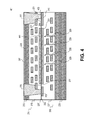
- FIG. 4 is a cross-section diagram illustrating yet another example of an integrated circuit system having first and second device wafers that are stacked and bonded together in an example integrated circuit system including integrated EMI shielding accordance with the teachings of the present invention.
- FIG. 5 is a cross-section diagram illustrating still another example of an integrated circuit system having first and second device wafers that are stacked and bonded together in an example integrated circuit system including integrated EMI shielding accordance with the teachings of the present invention.
- FIG. 6 is a illustrates an example top view of a stacked chip having a top metal layer that includes an example metal shield that is a solid piece in accordance with the teachings of the present invention.
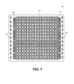
- FIG. 7 is a illustrates another example top view of a stacked chip having a top metal layer that includes an example metal shield that is a metal grid in accordance with the teachings of the present invention.
- FIG. 8 is a diagram illustrating one example of an imaging system including a pixel array having image sensor pixels included in an integrated circuit system having integrated EMI shielding in accordance with the teachings of the present invention.
- FIG. 1 is a diagram illustrating an example integrated circuit system 101 with stacked integrated circuit device wafers.
- integrated circuit system 101 includes a first device wafer 103 that is bonded to a second device wafer 111.
- First device wafer 103 includes a first semiconductor layer 105 and a first metal layer formed within a first metal layer oxide 107.
- conductors 109 and 119 are illustrated as being included in the first metal layer formed within the first metal layer oxide 107.
- Second device wafer 111 includes a having a second semiconductor layer 113 and a second metal layer formed within a second metal layer oxide 115.
- conductors 117 and 121 are illustrated as being included in the second metal layer formed within the second metal layer oxide 115.
- FIG. 1 also illustrates that conductive path 125 couples conductor 109 to conductor 117 and that conductive path 127 couples conductor 119 to conductor 121.
- conductive paths 125 and 127 are formed by inter-chip vias fabricated on a wafer-level.
- second device wafer 111 is thinned to thickness between 1-5 um.
- conductive paths 125 and 127 are formed with aspect ratios from 1-3 to couple first device wafer 103 to second device wafer 111. Due to the close proximity of first device wafer 103 to second device wafer 111, there is significant electrical interference or coupling between stacked first device wafer 103 to second device wafer 111, as illustrated with electromagnetic interference (EMI) 129.
- EMI electromagnetic interference
- EMI may be representative of electromagnetic interference, electrical interference, electrical coupling, or the like, that occurs between the stacked integrated circuit wafers in accordance with the teachings of the present invention.
- EMI 129 can cause undesirable effects and affect normal performance of first device wafer 103 and second device wafer 111.
- first device wafer 103 and second device wafer 111 are used to provide an image sensor, EMI 129 may introduce fixed pattern noise in the image sensor.
- FIG. 2 is a cross-section diagram illustrating an example of an integrated circuit system 201 having first and second device wafers that are stacked and bonded together in an example integrated circuit system including integrated EMI shielding in accordance with the teachings of the present invention.
- integrated circuit system 201 includes a first device wafer 203 having a first semiconductor layer 205 and a first metal layer disposed within a first metal layer oxide 207.
- Integrated circuit system 201 also includes a second device wafer 211 having a second semiconductor layer 213 and a second metal layer disposed within second metal layer oxide 215.
- first device wafer 203 includes an imager chip and second device wafer 211 includes a processing chip coupled to the imager chip.
- first semiconductor layer 205 includes silicon and second semiconductor layer includes thinned silicon.
- the first metal layer disposed within first metal layer oxide 207 includes a conductor 209 and a conductor 219.
- the illustrated example also shows that the second metal layer disposed within second metal layer oxide 207 includes a conductor 217 and a conductor 221.
- a frontside 235 of the first metal layer oxide 207 of the first device wafer 203 is bonded to a frontside 237 of the second metal layer oxide 215 of the second device wafer 211 at a bonding interface 223 between the first metal layer oxide 207 and the second metal layer oxide 215.
- a conductive path 225 couples conductor 209 to conductor 217.
- a conductive path 227 couples conductor 219 to the conductor 221.
- conductive paths 225 and 227 are formed by inter-chip vias fabricated on a wafer-level.
- conductive path 225 is formed in one example in a cavity etched between conductor 209 and conductor 227 and etched through bonding interface 223 and through second semiconductor layer 213 and through a passivation layer 247 from a backside 247 of second device wafer 211.
- conductive path 227 is further formed in a cavity etched through a hole 233 defined in the second conductor 221 and etched through bonding interface 223 and through the second semiconductor layer 213 and through passivation layer 247 from backside 247 of second device wafer 211.
- an EMI shield 231 is disposed in first metal oxide layer 207.
- EMI shield 231 is metal and is included in a metal layer disposed in the first metal oxide layer 207 that is nearest to the bonding interface 223 as shown.
- EMI shield 231 is included in the same metal layer as conductors 209 and/or 219, as shown in FIG. 2 .
- EMI shield 231 may be included in a metal layer disposed in second metal oxide layer 215. In the particular example illustrated in FIG.
- bonding interface 223 is an oxide-to-oxide interface between the first metal layer oxide 207 of first device wafer 203 and the second metal layer oxide 215 of second device wafer 211.
- EMI shield 231 in integrated system 201, even with the close proximity of first device wafer 203 to second device wafer 211, the EMI 229 that is generated in first device wafer 203 is shielded from affecting normal performance of second device wafer 211 in accordance with the teachings of the present invention as shown. Therefore, in an example integrated system 201 in which first device wafer 203 and second device wafer 211 are used to provide an image sensor, fixed pattern noise that could have been caused by EMI 229 is reduced or eliminated in accordance with the teachings of the present invention.
- FIG. 3 is a cross-section diagram illustrating another example of an integrated circuit system 301 having first and second device wafers that are stacked and bonded together in an example integrated circuit system including integrated EMI shielding accordance with the teachings of the present invention.
- integrated circuit system 301 of FIG. 3 shares similarities with integrated circuit system 201 of FIG. 2 , and like elements have kept their former labels.
- integrated circuit system 301 includes a first device wafer 203 having a first semiconductor layer 205 proximate to a first metal layer including a conductor 209 and a conductor 219 disposed within a first metal layer oxide 207.
- a second device wafer 211 having a second semiconductor layer 213 proximate to a second metal layer including a conductor 217 and a conductor 221 disposed within a second metal layer oxide 215.
- EMI shield 231, conductor 209 and conductor 219 in integrated circuit system 301 of FIG. 3 are at the bonding interface 323 in integrated circuit system 301.
- conductor 209 and conductor 219 are not at the bonding interface 323.
- bonding interface 323 includes an oxide-to-metal bonding interface that includes at least the bonding of metal EMI shield 231 with the oxide of second metal layer oxide 215 as shown.
- bonding interface 323 includes an oxide-to-metal bonding interface that includes at least the bonding of metal EMI shield 231 with the oxide of first metal layer oxide 207.
- the frontside 235 of the first metal layer oxide 207 of the first device wafer 203 is bonded to the frontside 237 of the second metal layer oxide 215 of the second device wafer 211 at the bonding interface 323 between the first device wafer 203 and the second device wafer 211.
- Conductive path 225 which couples the conductor 209 to the conductor 217, is formed in a cavity etched between conductor 209 and conductor 217 and etched through the bonding interface 323 and through the second semiconductor layer 213 from a backside 247 of the second device wafer 211.
- Conductive path 227 which couples the conductor 219 to the conductor 221, is formed in a cavity etched between conductor 219 and conductor 221 and etched through the bonding interface 323 and through the second semiconductor layer 213 from the backside 247 of the second device wafer 211.
- FIG. 4 is a cross-section diagram illustrating yet another example of an integrated circuit system 401 having first and second device wafers that are stacked and bonded together in an example integrated circuit system including integrated EMI shielding accordance with the teachings of the present invention.
- integrated circuit system 401 of FIG. 4 shares similarities with integrated circuit system 201 of FIG. 2 and integrated circuit system 301 of FIG. 3 , and like elements have kept their former labels.
- integrated circuit system 401 includes a first device wafer 203 having a first semiconductor layer 205 proximate to a first metal layer including conductor 209 and conductor 219 disposed within a first metal layer oxide 207.
- a second device wafer 211 having a second semiconductor layer 213 proximate to a second metal layer including a conductor 217 and a conductor 221 disposed within a second metal layer oxide 215.
- bonding interface 423 includes a metal-to-metal bonding interface that includes the bonding of metal EMI shield 231 to metal EMI shield 441 as shown.
- the metal EMI shields 231 and 442 have a large bonding surface area and therefore strengthen the wafer bonding between first device wafer 203 and second device wafer 211 in accordance with the teachings of the present invention.
- FIG. 5 is a cross-section diagram illustrating still another example of an integrated circuit system 501 having first and second device wafers that are stacked and bonded together in an example integrated circuit system including integrated EMI shielding accordance with the teachings of the present invention. It is appreciated that in the depicted example, integrated circuit system 401 of FIG. 4 shares similarities with integrated circuit system 201 of FIG. 2 , integrated circuit system 301 of FIG. 3 , and integrated circuit system 401 of FIG. 4 , and like elements have kept their former labels.
- integrated circuit system 501 includes a first device wafer 203 having a first semiconductor layer 205 proximate to a first metal layer including a conductor 209 and a conductor 219 disposed within a first metal layer oxide 207.
- a second device wafer 211 having a second semiconductor layer 213 proximate to a second metal layer including a conductor 517 and a conductor 521 disposed within a second metal layer oxide 215.
- bonding interface 423 includes a metal-to-metal bonding interfaces that include the bonding of conductor 209 to conductor 517, the bonding of conductor 219 to conductor 521, and the bonding of metal EMI shield 231 to metal EMI shield 441 as shown.
- the combined bonding surface areas of conductors 209, 517, 219 and 521 and metal EMI shields 231 and 442 are relatively large and therefore strengthen the wafer bonding between first device wafer 203 and second device wafer 211 in accordance with the teachings of the present invention.
- FIG. 6 is a illustrates an example top view of a device wafer 603 having a top metal layer that includes an example metal shield that is a solid piece in accordance with the teachings of the present invention.
- chip 603 may correspond for example with at least first device wafer 203 of FIGs. 3-5 .
- a top view of device wafer 603 is shown including an EMI shield 631 with inter-chip bonding pads 609 and 619 as well as external bonding pads 643 and 645, which are disposed in a top metal layer of device wafer 603.
- EMI shield 631 includes metal and is a solid piece as illustrated.
- FIG. 7 is a illustrates another example top view of a device wafer 703 having a top metal layer that includes an example metal shield that is a metal grid in accordance with the teachings of the present invention.
- chip 703 may correspond for example with at least first device wafer 203 of FIGs. 3-5 .
- a top view of device wafer 703 is shown including an EMI shield 731 with inter-chip bonding pads 709 and 719 as well as external bonding pads 743 and 745, which are disposed in a top metal layer of device wafer 603.
- EMI shield 731 includes metal and is a metal grid as illustrated.
- the metal grid of EMI shield 731 is fabricated using copper damascene for top metal layer patterning.
- the openings of the metal grid of EMI shield 731 are substantially smaller than a wavelength of electrical interference generated within an integrated circuit system including device 703 in accordance with the teachings of the present invention.
- FIG. 8 is a diagram illustrating one example of an imaging system 800 including an example pixel array 802 having a plurality of image sensor pixels included in an example integrated circuit system featuring integrated EMI shielding in accordance with the teachings of the present invention. As shown in the depicted example, imaging system 800 includes pixel array 802 coupled to control circuitry 808 and readout circuitry 804, which is coupled to function logic 806.
- pixel array 802 is a two-dimensional (2D) array of image sensor pixels (e.g. , pixels P1, P2 ..., Pn).
- pixel array 802 is included in an integrated circuit system, such as for example integrated circuit system 201, 302, 401 or 501, as discussed above in FIGs. 2-5 . Therefore, pixel array 802 has substantially little or no fixed pattern noise that results from electrical interference or electrical coupling because of the integrated EMI shielding included in pixel array 802 in accordance with the teachings of the present invention.
- each pixel is arranged into a row (e.g., rows R1 to Ry) and a column ( e.g. , column C1 to Cx) to acquire image data of a person, place, object, etc., which can then be used to render a 2D image of the person, place, object, etc.
- readout circuitry 804 may include amplification circuitry, analog-to-digital (ADC) conversion circuitry, or otherwise.
- Function logic 806 may simply store the image data or even manipulate the image data by applying post image effects (e.g. , crop, rotate, remove red eye, adjust brightness, adjust contrast, or otherwise).
- readout circuitry 804 may readout a row of image data at a time along readout column lines (illustrated) or may readout the image data using a variety of other techniques (not illustrated), such as a serial readout or a full parallel readout of all pixels simultaneously.
- control circuitry 808 is coupled to pixel array 802 to control operational characteristics of pixel array 502.
- control circuitry 808 may generate a shutter signal for controlling image acquisition.
- the shutter signal is a global shutter signal for simultaneously enabling all pixels within pixel array 802 to simultaneously capture their respective image data during a single acquisition window.
- the shutter signal is a rolling shutter signal such that each row, column, or group of pixels is sequentially enabled during consecutive acquisition windows.
Landscapes
- Semiconductor Integrated Circuits (AREA)
- Internal Circuitry In Semiconductor Integrated Circuit Devices (AREA)
- Solid State Image Pick-Up Elements (AREA)
- Shielding Devices Or Components To Electric Or Magnetic Fields (AREA)
Applications Claiming Priority (1)
| Application Number | Priority Date | Filing Date | Title |
|---|---|---|---|
| US13/547,997 US8933544B2 (en) | 2012-07-12 | 2012-07-12 | Integrated circuit stack with integrated electromagnetic interference shielding |
Publications (2)
| Publication Number | Publication Date |
|---|---|
| EP2685503A2 true EP2685503A2 (de) | 2014-01-15 |
| EP2685503A3 EP2685503A3 (de) | 2014-02-12 |
Family
ID=48628555
Family Applications (1)
| Application Number | Title | Priority Date | Filing Date |
|---|---|---|---|
| EP13172952.7A Withdrawn EP2685503A3 (de) | 2012-07-12 | 2013-06-20 | Integrierter Schaltungsstapel mit integrierter elektromagnetischer Interferenzabschirmung |
Country Status (4)
| Country | Link |
|---|---|
| US (1) | US8933544B2 (de) |
| EP (1) | EP2685503A3 (de) |
| CN (1) | CN103545296B (de) |
| TW (1) | TWI533430B (de) |
Cited By (2)
| Publication number | Priority date | Publication date | Assignee | Title |
|---|---|---|---|---|
| CN105742197A (zh) * | 2016-03-11 | 2016-07-06 | 武汉新芯集成电路制造有限公司 | 一种键合晶圆结构及其制备方法 |
| CN105977236A (zh) * | 2016-05-30 | 2016-09-28 | 武汉新芯集成电路制造有限公司 | 键合晶圆结构及其制备方法 |
Families Citing this family (22)
| Publication number | Priority date | Publication date | Assignee | Title |
|---|---|---|---|---|
| US9478579B2 (en) | 2012-10-16 | 2016-10-25 | Omnivision Technologies, Inc. | Stacked chip image sensor with light-sensitive circuit elements on the bottom chip |
| US20150187701A1 (en) | 2013-03-12 | 2015-07-02 | Taiwan Semiconductor Manufacturing Company, Ltd. | Semiconductor Devices and Methods of Manufacture Thereof |
| TWI631854B (zh) * | 2013-08-05 | 2018-08-01 | 日商新力股份有限公司 | Conversion device, imaging device, electronic device, conversion method |
| US10056353B2 (en) | 2013-12-19 | 2018-08-21 | Taiwan Semiconductor Manufacturing Company, Ltd. | 3DIC interconnect apparatus and method |
| US9713255B2 (en) * | 2014-02-19 | 2017-07-18 | Intel Corporation | Electro-magnetic interference (EMI) shielding techniques and configurations |
| US9449914B2 (en) | 2014-07-17 | 2016-09-20 | Taiwan Semiconductor Manufacturing Company, Ltd. | Stacked integrated circuits with redistribution lines |
| TWI747805B (zh) * | 2014-10-08 | 2021-12-01 | 日商索尼半導體解決方案公司 | 攝像裝置及製造方法、以及電子機器 |
| US9505609B2 (en) * | 2015-04-29 | 2016-11-29 | Invensense, Inc. | CMOS-MEMS integrated device with selective bond pad protection |
| CN105140217B (zh) * | 2015-07-27 | 2018-03-02 | 武汉新芯集成电路制造有限公司 | 一种三维集成器件的制备方法 |
| CN105047649A (zh) * | 2015-07-27 | 2015-11-11 | 武汉新芯集成电路制造有限公司 | 一种三维集成芯片结构及其制备方法 |
| CN106611756A (zh) * | 2015-10-26 | 2017-05-03 | 联华电子股份有限公司 | 晶片对晶片对接结构及其制作方法 |
| CN105826214B (zh) * | 2016-05-30 | 2019-04-30 | 武汉新芯集成电路制造有限公司 | 一种键合晶圆结构的制备方法 |
| US9992437B1 (en) | 2017-02-03 | 2018-06-05 | SmartSense Technology(U.S.), Inc. | Stacked image sensor pixel cell with in-pixel vertical channel transfer transistor |
| US10051218B1 (en) | 2017-02-03 | 2018-08-14 | SmartSens Technology (U.S.), Inc. | Stacked image sensor pixel cell with in-pixel vertical channel transfer transistor and reflective structure |
| CN108155198B (zh) * | 2017-12-22 | 2021-04-02 | 成都先锋材料有限公司 | 一种cmos影像传感封装结构及其制作方法 |
| CN107946335B (zh) * | 2017-12-22 | 2020-10-27 | 成都先锋材料有限公司 | 一种cmos影像传感封装结构及其制作方法 |
| CN108281412B (zh) * | 2018-01-23 | 2020-02-14 | 德淮半导体有限公司 | 堆叠式图像传感器、像素管芯及其制造方法 |
| JP7402606B2 (ja) * | 2018-10-31 | 2023-12-21 | ソニーセミコンダクタソリューションズ株式会社 | 固体撮像装置及び電子機器 |
| US11037885B2 (en) | 2019-08-12 | 2021-06-15 | Taiwan Semiconductor Manufacturing Co., Ltd. | Semiconductor packaging device comprising a shield structure |
| KR102887278B1 (ko) | 2020-12-17 | 2025-11-17 | 삼성전자주식회사 | 이미지 센서 |
| KR20220127624A (ko) | 2021-03-11 | 2022-09-20 | 에스케이하이닉스 주식회사 | 이미지 센싱 장치 |
| WO2024160459A1 (en) * | 2023-01-31 | 2024-08-08 | Ams-Osram Ag | Wafer structure, optical sensor, and corresponding method of production |
Family Cites Families (15)
| Publication number | Priority date | Publication date | Assignee | Title |
|---|---|---|---|---|
| US4785341A (en) | 1979-06-29 | 1988-11-15 | International Business Machines Corporation | Interconnection of opposite conductivity type semiconductor regions |
| US6627999B2 (en) * | 2000-08-31 | 2003-09-30 | Micron Technology, Inc. | Flip-chip with matched signal lines, ground plane and ground bumps adjacent signal bumps |
| US6730540B2 (en) * | 2002-04-18 | 2004-05-04 | Tru-Si Technologies, Inc. | Clock distribution networks and conductive lines in semiconductor integrated circuits |
| US6927432B2 (en) | 2003-08-13 | 2005-08-09 | Motorola, Inc. | Vertically integrated photosensor for CMOS imagers |
| CN1665025A (zh) * | 2004-03-05 | 2005-09-07 | 硕达科技股份有限公司 | 可避免电磁干扰的半导体封装件及其制法 |
| US20100103634A1 (en) * | 2007-03-30 | 2010-04-29 | Takuo Funaya | Functional-device-embedded circuit board, method for manufacturing the same, and electronic equipment |
| US7965329B2 (en) | 2008-09-09 | 2011-06-21 | Omnivision Technologies, Inc. | High gain read circuit for 3D integrated pixel |
| WO2010056359A1 (en) * | 2008-11-14 | 2010-05-20 | Optoelectronic Systems Consulting, Inc. | Miniaturized implantable sensor platform having multiple devices and sub-chips |
| DE102009004409A1 (de) * | 2009-01-13 | 2010-07-15 | Arnold & Richter Cine Technik Gmbh & Co. Betriebs Kg | Bildsensor |
| US8415238B2 (en) * | 2010-01-14 | 2013-04-09 | International Business Machines Corporation | Three dimensional integration and methods of through silicon via creation |
| US20120061789A1 (en) | 2010-09-13 | 2012-03-15 | Omnivision Technologies, Inc. | Image sensor with improved noise shielding |
| JP2012064709A (ja) | 2010-09-15 | 2012-03-29 | Sony Corp | 固体撮像装置及び電子機器 |
| JP2012094720A (ja) | 2010-10-27 | 2012-05-17 | Sony Corp | 固体撮像装置、半導体装置、固体撮像装置の製造方法、半導体装置の製造方法、及び電子機器 |
| CN102412228B (zh) * | 2011-10-31 | 2014-04-02 | 中国科学院微电子研究所 | 同轴硅通孔互连结构及其制造方法 |
| US20130264688A1 (en) * | 2012-04-06 | 2013-10-10 | Omnivision Technologies, Inc. | Method and apparatus providing integrated circuit system with interconnected stacked device wafers |
-
2012
- 2012-07-12 US US13/547,997 patent/US8933544B2/en active Active
-
2013
- 2013-05-13 TW TW102116918A patent/TWI533430B/zh active
- 2013-06-05 CN CN201310222125.4A patent/CN103545296B/zh active Active
- 2013-06-20 EP EP13172952.7A patent/EP2685503A3/de not_active Withdrawn
Cited By (4)
| Publication number | Priority date | Publication date | Assignee | Title |
|---|---|---|---|---|
| CN105742197A (zh) * | 2016-03-11 | 2016-07-06 | 武汉新芯集成电路制造有限公司 | 一种键合晶圆结构及其制备方法 |
| CN105742197B (zh) * | 2016-03-11 | 2018-08-24 | 武汉新芯集成电路制造有限公司 | 一种键合晶圆结构及其制备方法 |
| CN105977236A (zh) * | 2016-05-30 | 2016-09-28 | 武汉新芯集成电路制造有限公司 | 键合晶圆结构及其制备方法 |
| CN105977236B (zh) * | 2016-05-30 | 2018-09-21 | 武汉新芯集成电路制造有限公司 | 键合晶圆结构及其制备方法 |
Also Published As
| Publication number | Publication date |
|---|---|
| US8933544B2 (en) | 2015-01-13 |
| CN103545296B (zh) | 2016-09-21 |
| TW201403786A (zh) | 2014-01-16 |
| CN103545296A (zh) | 2014-01-29 |
| US20140014813A1 (en) | 2014-01-16 |
| TWI533430B (zh) | 2016-05-11 |
| EP2685503A3 (de) | 2014-02-12 |
Similar Documents
| Publication | Publication Date | Title |
|---|---|---|
| US8933544B2 (en) | Integrated circuit stack with integrated electromagnetic interference shielding | |
| US20250160031A1 (en) | Electronic device package and fabricating method thereof | |
| US10930699B2 (en) | Method and apparatus for image sensor packaging | |
| US10580815B2 (en) | Solid state imaging device and electronic apparatus | |
| US9337227B2 (en) | Multi-substrate image sensor having a dual detection function | |
| CN103094293B (zh) | 用于半导体装置中的衬垫下电路的衬垫设计 | |
| EP2717300B1 (de) | Halbleiterbauelement | |
| US20130264688A1 (en) | Method and apparatus providing integrated circuit system with interconnected stacked device wafers | |
| US10192919B2 (en) | Imaging systems with backside isolation trenches | |
| CN102403328B (zh) | 具有改良噪声屏蔽的图像传感器 | |
| US9041134B2 (en) | Solid-state imaging device | |
| EP2571056A2 (de) | Zweiseitige Kameraanordnung | |
| US20150171132A1 (en) | Image Sensor Devices, Methods of Manufacture Thereof, and Semiconductor Device Manufacturing Methods | |
| KR20180032914A (ko) | 팬-아웃 센서 패키지 및 이를 포함하는 카메라 모듈 | |
| KR20140008983A (ko) | 이미지 센서 패키징을 위한 방법 및 장치 | |
| US20140326856A1 (en) | Integrated circuit stack with low profile contacts | |
| US9847364B2 (en) | Image sensor devices and design and manufacturing methods thereof | |
| US10651218B1 (en) | Optical sensor structure and method for forming the same | |
| HK1190824A (en) | Integrated circuit stack with integrated electromagnetic interference shielding | |
| HK1190824B (en) | Integrated circuit stack with integrated electromagnetic interference shielding | |
| US8956909B2 (en) | Method of fabricating an electronic device comprising photodiode | |
| KR20220002241A (ko) | 광학 센서 디바이스 및 광학 센서 디바이스를 제조하기 위한 방법 | |
| US8835992B2 (en) | Electronic device comprising electrical contact pads | |
| US20220013562A1 (en) | Image sensing device | |
| HK1183161B (en) | Pad design for circuit under pad in semiconductor devices |
Legal Events
| Date | Code | Title | Description |
|---|---|---|---|
| PUAL | Search report despatched |
Free format text: ORIGINAL CODE: 0009013 |
|
| PUAI | Public reference made under article 153(3) epc to a published international application that has entered the european phase |
Free format text: ORIGINAL CODE: 0009012 |
|
| AK | Designated contracting states |
Kind code of ref document: A2 Designated state(s): AL AT BE BG CH CY CZ DE DK EE ES FI FR GB GR HR HU IE IS IT LI LT LU LV MC MK MT NL NO PL PT RO RS SE SI SK SM TR |
|
| AX | Request for extension of the european patent |
Extension state: BA ME |
|
| AK | Designated contracting states |
Kind code of ref document: A3 Designated state(s): AL AT BE BG CH CY CZ DE DK EE ES FI FR GB GR HR HU IE IS IT LI LT LU LV MC MK MT NL NO PL PT RO RS SE SI SK SM TR |
|
| AX | Request for extension of the european patent |
Extension state: BA ME |
|
| RIC1 | Information provided on ipc code assigned before grant |
Ipc: H01L 27/146 20060101AFI20140109BHEP |
|
| STAA | Information on the status of an ep patent application or granted ep patent |
Free format text: STATUS: THE APPLICATION IS DEEMED TO BE WITHDRAWN |
|
| 18D | Application deemed to be withdrawn |
Effective date: 20140813 |