EP2685501A1 - Circuit integre sur soi comprenant un transistor de protection sous-jacent - Google Patents
Circuit integre sur soi comprenant un transistor de protection sous-jacent Download PDFInfo
- Publication number
- EP2685501A1 EP2685501A1 EP13175436.8A EP13175436A EP2685501A1 EP 2685501 A1 EP2685501 A1 EP 2685501A1 EP 13175436 A EP13175436 A EP 13175436A EP 2685501 A1 EP2685501 A1 EP 2685501A1
- Authority
- EP
- European Patent Office
- Prior art keywords
- transistor
- integrated circuit
- type
- ground plane
- doping
- Prior art date
- Legal status (The legal status is an assumption and is not a legal conclusion. Google has not performed a legal analysis and makes no representation as to the accuracy of the status listed.)
- Withdrawn
Links
- 238000002955 isolation Methods 0.000 claims abstract description 36
- 239000004065 semiconductor Substances 0.000 claims abstract description 35
- 239000002019 doping agent Substances 0.000 claims description 13
- 230000005669 field effect Effects 0.000 claims description 8
- 229910052710 silicon Inorganic materials 0.000 abstract description 7
- 239000010703 silicon Substances 0.000 abstract description 7
- 239000012212 insulator Substances 0.000 abstract description 6
- 239000000758 substrate Substances 0.000 description 17
- 230000010287 polarization Effects 0.000 description 7
- XUIMIQQOPSSXEZ-UHFFFAOYSA-N Silicon Chemical compound [Si] XUIMIQQOPSSXEZ-UHFFFAOYSA-N 0.000 description 6
- 238000009413 insulation Methods 0.000 description 6
- 238000010586 diagram Methods 0.000 description 4
- 230000010354 integration Effects 0.000 description 3
- 239000000463 material Substances 0.000 description 3
- 230000001965 increasing effect Effects 0.000 description 2
- VYPSYNLAJGMNEJ-UHFFFAOYSA-N Silicium dioxide Chemical compound O=[Si]=O VYPSYNLAJGMNEJ-UHFFFAOYSA-N 0.000 description 1
- 230000004069 differentiation Effects 0.000 description 1
- 230000000694 effects Effects 0.000 description 1
- 230000005684 electric field Effects 0.000 description 1
- 230000001939 inductive effect Effects 0.000 description 1
- 230000005865 ionizing radiation Effects 0.000 description 1
- 239000002184 metal Substances 0.000 description 1
- 230000003071 parasitic effect Effects 0.000 description 1
- 230000000135 prohibitive effect Effects 0.000 description 1
- 230000001681 protective effect Effects 0.000 description 1
- 230000005855 radiation Effects 0.000 description 1
- 229910052814 silicon oxide Inorganic materials 0.000 description 1
- 230000003068 static effect Effects 0.000 description 1
Images

Classifications
-
- H—ELECTRICITY
- H10—SEMICONDUCTOR DEVICES; ELECTRIC SOLID-STATE DEVICES NOT OTHERWISE PROVIDED FOR
- H10D—INORGANIC ELECTRIC SEMICONDUCTOR DEVICES
- H10D30/00—Field-effect transistors [FET]
- H10D30/01—Manufacture or treatment
- H10D30/021—Manufacture or treatment of FETs having insulated gates [IGFET]
-
- H—ELECTRICITY
- H10—SEMICONDUCTOR DEVICES; ELECTRIC SOLID-STATE DEVICES NOT OTHERWISE PROVIDED FOR
- H10D—INORGANIC ELECTRIC SEMICONDUCTOR DEVICES
- H10D87/00—Integrated devices comprising both bulk components and either SOI or SOS components on the same substrate
-
- H—ELECTRICITY
- H10—SEMICONDUCTOR DEVICES; ELECTRIC SOLID-STATE DEVICES NOT OTHERWISE PROVIDED FOR
- H10D—INORGANIC ELECTRIC SEMICONDUCTOR DEVICES
- H10D89/00—Aspects of integrated devices not covered by groups H10D84/00 - H10D88/00
- H10D89/60—Integrated devices comprising arrangements for electrical or thermal protection, e.g. protection circuits against electrostatic discharge [ESD]
- H10D89/601—Integrated devices comprising arrangements for electrical or thermal protection, e.g. protection circuits against electrostatic discharge [ESD] for devices having insulated gate electrodes, e.g. for IGFETs or IGBTs
- H10D89/931—Integrated devices comprising arrangements for electrical or thermal protection, e.g. protection circuits against electrostatic discharge [ESD] for devices having insulated gate electrodes, e.g. for IGFETs or IGBTs characterised by the dispositions of the protective arrangements
-
- H—ELECTRICITY
- H10—SEMICONDUCTOR DEVICES; ELECTRIC SOLID-STATE DEVICES NOT OTHERWISE PROVIDED FOR
- H10D—INORGANIC ELECTRIC SEMICONDUCTOR DEVICES
- H10D88/00—Three-dimensional [3D] integrated devices
Definitions
- the invention relates to integrated circuits, and in particular integrated circuits made on a silicon-on-insulator (SOI) type substrate.
- SOI technology consists of separating a thin layer of silicon (a few nanometers) on a silicon substrate by a relatively thick insulating layer (a few tens of nanometers as a rule).
- Integrated circuits made in SOI technology have a number of advantages. Such circuits generally have lower power consumption for equivalent performance. Such circuits also induce lower parasitic capacitances, which make it possible to improve the switching speed. In addition, the phenomenon of latchup in the English language encountered by MOS transistors Bulk technology can be avoided. Such circuits are therefore particularly suitable for SoC or MEMS type applications. It can also be seen that the SOI integrated circuits are less sensitive to the effects of ionizing radiation and thus prove more reliable in applications where such radiations can induce operating problems, especially in space applications.
- the SOI integrated circuits can notably comprise SRAM-type random access devices or logic gates.
- the doping level of the channel of the transistors can not therefore present significant variations, which prevents differentiation of the threshold voltages by this means.
- a solution proposed in certain studies for producing transistors of the same type with distinct threshold voltages is to integrate different gate materials for these transistors.
- the practical realization of such an integrated circuit is technically delicate and economically prohibitive.
- the transistors are generally surrounded by insulation trenches (referred to as STI for Shallow Trench Isolation in English) that extend to the caissons.
- STI Shallow Trench Isolation in English
- Such integrated circuits also include protection devices against electrostatic discharges (ESD for "Electrostatic Discharge” in English) accidental and can deteriorate these transistors.
- ESD electrostatic Discharge
- the document US2012 / 056273 discloses an integrated circuit comprising a field effect transistor disposed on a buried insulating layer.
- a ground plane is disposed vertically above the gate and the transistor channel, beneath the buried insulating layer.
- the invention proposes to use, in an integrated circuit, isolation trenches of depth and reduced dimensions in order to provide an ESD protection device of the integrated circuit.
- a protective device is formed of a transistor, formed under an electronic component. This protection device does not affect the integration density of the circuit and provides protection against electrostatic discharge by deriving a large discharge current.
- the figure 1 is a schematic top view of a portion of an integrated circuit manufactured on SOI, in section at ground planes and implanted areas.
- the integrated circuit here comprises a field effect transistor 1.
- the figure 2 is a cross-sectional view of the integrated circuit.
- the transistor 1 is made in a layer of a semiconductor material, called an active layer, formed on an insulating layer 92, this insulating layer 92 being formed in line with a semiconductor substrate 91, typically doped with type p.
- Transistor 1 is for example an nMOS transistor.
- the nMOS transistor is generally aligned with other nMOS transistors in a row of cells, each cell including an nMOS transistor and a pMOS transistor.
- the transistor 1 comprises, in a manner known per se, a source, a drain and a channel, and a gate stack made directly above the channel.
- the source, the drain and the channel of the transistor 1 are formed in the semiconductor active layer 15.
- the transistor 1 comprises a gate stack 16 disposed on the semiconductor active layer 15, in line with its channel.
- the transistor of the active layer may, in a manner known per se, be of the FDSOI type (for "Fully Depleted Silicon On Insulator" in English) with a channel of lightly doped semiconductor material, the channel having a dopant concentration substantially equal to the dopant concentration of the substrate 91.
- the transistor 1 also comprises source and drain electrodes, not illustrated, on which the potentials Es and Ed are respectively applied.
- a semiconductor ground plane 11 is formed in line with the transistor 1, under the buried insulating layer 92.
- the doping of the ground plane 11 is of type n.
- the ground plane 11 extends under most of the buried insulating layer.
- the ground plane 11 extends vertically above the gate stack 16 and the channel of the transistor 1.
- the ground plane 11 is biased by a semiconductor implanted zone 18, at a potential E1.
- the implanted zone 18 has a doping of type n (and preferably N + doping).
- the polarization of the ground plane 11 can be carried out via a bias circuit not shown here.
- An isolation trench 62 is provided in line with the contact between the ground plane 11 and the implanted zone 18.
- the isolation trench 62 passes through the insulating layer 92 and thus extends to the ground plane 11.
- the trench 62 does not reach the bottom of the ground plane 11 or the implanted zone 18, in order to preserve contact between them.
- the isolation trench 62 makes it possible to improve the isolation between the transistor 1 and the implanted zone 18.
- Insulation trenches 61 and 65 are also provided on the periphery, in order to isolate the transistor 1, with respect to the underlying elements which will be detailed, and with respect to the electrodes of these elements.
- the isolation trench 61 is formed at a border of the implanted zone 18.
- the trench 61 extends through the buried insulating layer 92 to the caisson 12, without reaching the substrate 91.
- the trench 61 can present the same depth as the trench 62 to form a lateral protection diode. 18.
- a semiconductor zone 13 is formed in line with the transistor 1, under the buried insulating layer 92. The doping of the zone 13 and of the n-type. Zone 13 is placed in line with the drain of transistor 1, at a border of this transistor. The zone 13 is offset laterally with respect to the gate stack 16.
- the zone 13 is polarized by a semiconductor implanted zone 14 at a potential E2.
- the implanted zone 14 has n-type doping (and preferably N + doping).
- the polarization of the zone 13 can be carried out via the polarization circuit mentioned above.
- An isolation trench 63 is provided above the contact between the zone 13 and the implanted zone 14.
- the isolation trench 63 passes through the insulating layer 92 and thus extends to the zone 13.
- the trench the insulation 63 advantageously has the same depth as the isolation trench 62.
- the trench 63 does not reach the bottom of the zone 13 or the implanted zone 14, in order to preserve contact between them.
- the isolation trench 63 makes it possible to improve the insulation between the transistor 1 and the implanted zone 14.
- a semiconductor box 12 is formed in line with the ground plane 11 and the zone 13.
- the doping of the box 12 is p-type.
- the box 12 extends laterally above the implanted areas 14 and 18.
- the box 12 further comprises a portion 19 extending vertically upwards and separating the zone 13 from the ground plane 11.
- the portion 19 forms a lower channel between the zone 13 and the ground plane 11.
- the lower channel 19 is offset laterally with respect to the gate stack 16, and disposed vertically above an electrode of the transistor 1 (in this case the drain ).
- the zone 19 may have a width of 0.2 ⁇ m and is advantageously between 0.1 and 0.3 ⁇ m.
- the zone 19 may have a thickness equivalent to the thickness of the ground plane 11.
- the bottoms of the implanted zones 14 and 18 are in contact with the casing 12.
- the implanted zone 18 makes it possible both to polarize the ground plane 11, and to form an electrode for a device for protection against electrostatic discharges between two potentials.
- the implanted zone 14 forms another electrode for this protection device.
- the casing 12 is polarized by a semiconductor implanted zone 17 at a potential E3.
- the implanted zone 17 has p-type (and preferably P + doping) doping.
- the polarization of the box 12 can be carried out via the polarization circuit mentioned above.
- the bottom of the implanted zone 17 is in contact with the caisson 12.
- the implanted zone 17 is formed between the isolation trench 65 and an isolation trench 64.
- the isolation trenches 64 and 65 extend through the buried insulating layer 92 to the caisson 12, without reaching the substrate 91.
- the casing 12 thus extends laterally to the base of the implanted zone 17, under the isolation trenches 62, 63 and 64.
- the isolation trenches 64 and 65 advantageously have the same depth.
- the implanted zones 14, 17 and 18 are coplanar with the ground plane 11, the lower channel 19, and the zone 13.
- coplanar means that it is possible to define a plane parallel to the layer 92 and passing through the zones concerned. .
- the buried insulating layer 92 in a manner known per se, electrically isolates the transistor 1 from its ground plane 11, its box 12, and the substrate 91.
- the substrate 91 may for example be biased to a ground voltage Gnd.
- the buried insulating layer 92 formed above the transistor is here UTBOX type ("Ultra-Thin Buried Oxide Layer" in English).
- the control of the polarization of the ground plane 11 (also called back gate, or 'back gate' in English language) makes it possible to modulate the threshold voltage of the transistor 1.
- the ground plane 11 extending under the channel of the transistor 1, its bias makes it possible to influence the threshold voltage of this transistor.
- the insulating layer 92 has for example a thickness less than or equal to 60 nm, less than or equal to 50 nm, or less than or equal to 20 nm.
- the insulating layer 92 may be made in a manner known per se in silicon oxide.
- An underlying field effect transistor 2 of nMOS type is thus formed under the transistor 1.
- the drain of this transistor 2 is here formed by the association of the implanted zone 14 and the zone 13, and its source is formed by the combination of the implanted zone 18 and the ground plane 11.
- the lower channel 19 forms the channel of this transistor 2.
- the buried insulating layer 92 is here used as gate insulator.
- An electrode of the transistor 1, in this case the drain, is used as a gate for this transistor 2.
- the transistor 2 can be turned on to ensure a discharge between the potentials E1 and E2 (corresponding for example to potentials defined by the power supply rails of the integrated circuit) through the box 12 , and thus protect connected components between these potentials.
- the depth of the trenches 62 and 63 makes it possible to adjust the drain and source access resistances of the transistor 2.
- the depth of the trenches 62 and 63 also makes it possible to adjust the ballast resistance in the event of triggering the "snapback" phenomenon. ", Allowing a uniformization of the discharge current.
- the casing 12 may have dopant concentrations of between 10 16 cm -3 and 10 18 cm -3 .
- the ground plane 11 and the zone 13 may have dopant concentrations of between 10 18 cm -3 and 10 19 cm -3 .
- the lower channel 19 may have a concentration of dopants identical to those of the ground plane 11 and the zone 13 or the box 12.
- the box 12 can extend to a depth of less than 1 .mu.m and, preferably, lower or equal to 700nm.
- Metal contacts may be deposited after siliciding directly on each of the implanted zones 14, 17 and 18, to allow electrical connection of each of them.
- the implanted zones 14, 17 and 18 each have a concentration of dopants at least fifty times, or a hundred times greater than the dopant concentration of the box 12.
- the implanted zones 14, 17 and 18 have concentrations of dopants advantageously greater than or equal to 5 * 10 18 cm -3 and preferably between 10 19 cm -3 and 10 21 cm -3 .
- These dopant concentrations are, for example, substantially equal to the dopant concentrations of the source or the drain of the transistor 1.
- the implanted zones 14, 17 and 18 are formed laterally with respect to the transistor 1.
- the figure 3 is a cross-sectional view of a particular case of configuration of the integrated circuit of the Figures 1 and 2 .
- the drain potential Ed is applied to the implanted zone 14, and the source potential Es is applied to the implanted zone 18.
- a ground potential Gnd is here applied to the implanted zone 17 and to the semiconductor substrate. driver 91.
- the figure 4 is a circuit diagram of an example of application of the integrated circuit of the figure 3 .
- the nMOS transistor 1 is here an electronic component that is to be protected locally against electrostatic discharges.
- the drain of transistor 1 is used as the gate of transistor 2.
- the drains of transistors 1 and 2 are at potential Ed and the sources of transistors 1 and 2 are at potential Es.
- the substrate 91 is used as the body (for body in English) of the transistor 2 biased at the potential Gnd.
- the box 12 can also be isolated from the substrate 91 using a deep layer of insulation.
- the body of the transistor 2 can then be polarized with a potential different from the substrate 91 which is grounded.
- the transistor 2 closes to derive the electrostatic discharge under the transistor 1, between the potentials Ed and Es.
- the transistor 2 thus provides local protection against electrostatic discharges, making it possible to derive a large discharge current with a reduced tripping time.
- the transistor 2 formed being for the most part placed under the transistor 1, it induces only a limited drop in integration density for the integrated circuit.
- the figure 5 is a circuit diagram of another application for a variant of the integrated circuit of the figure 3 .
- the nMOS transistor 1 is intended to control the transistor 2 formed, to provide centralized protection for other components of the integrated circuit, between the potentials Ed and Es.
- the substrate 91 is biased at the ground potential Gnd.
- the ground plane 11 of the transistor 1 is here arranged in line with its drain, the zone 13 is arranged in line with its source, the zone 19 is arranged in line with its source and is offset laterally with respect to its source. at the gate stack 16.
- the source of the transistor 1 is used as the gate of the transistor 2.
- the drain of the transistor 1 and the implanted zone 14 are biased at the potential Ed.
- the source of the transistor 1 and the implanted zone 18 are polarized at the potential Es.
- the body of the transistor 2 can also be connected to the gate and therefore to the potential Es, thus lowering the threshold voltage of the transistor 2.
- a resistor R1 is formed between the source of transistor 1 and the potential Es.
- a resistor R2 is formed between the gate of transistor 1 and the potential Ed.
- An electrostatic discharge inducing an elevation of potential Es closes transistor 1, and causes the closing of transistor 2.
- Transistor 1 thus makes it possible to control the closing of transistor 2 in the presence of such an electrostatic discharge.
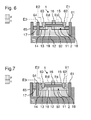
- the figure 6 is a cross-sectional view of another embodiment of an integrated circuit.
- the field effect transistor 1 is realized in the active layer 15, formed on the insulating layer 92, formed in line with the semiconductor substrate 91 (p-type doping).
- Transistor 1 is also of the FDSOI type.
- the transistor 1 comprises a source, a drain and a channel, and a gate stack 16 made directly above the channel.
- the source, the drain and the channel of the transistor 1 are formed in the active layer 15.
- Potential Es and Ed are respectively applied to the source and drain electrodes of the transistor 1.
- the semiconductor ground plane 11 (formed perpendicular to the transistor 1 beneath the buried insulating layer 92) exhibits p-type doping.
- the ground plane 11 extends under most of the buried insulating layer.
- the ground plane 11 extends vertically above the gate stack 16 and the channel of the transistor 1.
- the ground plane 11 is biased by the semiconductor implanted zone 18 to a potential E1.
- the implanted zone 18 has a p-type doping (and preferably a P + doping).
- the isolation trench 62 is formed in line with the contact between the ground plane 11 and the implanted zone 18.
- the isolation trench 62 passes through the insulating layer 92 and thus extends to the ground plane 11.
- the trench 62 does not reach the bottom of the ground plane 11 or the implanted zone 18, in order to preserve contact between them.
- the isolation trenches 61 and 65 are moreover arranged peripherally, in order to isolate the transistor 1, with respect to the underlying elements, and with respect to the electrodes of these elements.
- the isolation trench 61 is formed at a border of the implanted zone 18.
- the trench 61 here has the same depth as the trench 64, and therefore extends through the insulating layer 62 until it contacts the trench. implanted area 18.
- Zone 13 (formed perpendicular to the transistor 1, under the buried insulating layer 92) has a p-type doping. Zone 13 is placed in line with the drain of transistor 1, at a border of this transistor. The zone 13 is offset laterally with respect to the gate stack 16.
- the zone 13 is polarized by the implanted zone 14 semi-conductor, at a potential E2.
- the implanted zone 14 has a p-type doping (and preferably a P + doping).
- the isolation trench 63 is formed in line with the contact between the zone 13 and the implanted zone 14.
- the isolation trench 63 passes through the insulating layer 92 and thus extends to the zone 13.
- the trench the insulation 63 advantageously has the same depth as the isolation trench 62.
- the trench 63 does not reach the bottom of the zone 13 or the implanted zone 14, in order to preserve contact between them.
- the semiconductor casing 12 is formed in line with the ground plane 11 and the zone 13.
- the doping of the casing 12 is of type n.
- the box 12 extends laterally above the implanted zones 14 and 18.
- the portion 19 of the box 12 extends vertically upwards and separates the zone 13 from the ground plane 11.
- the portion 19 forms a lower channel between the zone 13 and the ground plane 11.
- the lower channel 19 is offset laterally relative to the gate stack 16, and disposed vertically above an electrode of the transistor 1 (in this case the drain).
- the bottoms of the implanted zones 14 and 18 are in contact with the casing 12.
- the implanted zone 18 makes it possible both to polarize the ground plane 11, and to form an electrode for a device for protection against electrostatic discharges between two potentials.
- the implanted zone 14 forms another electrode for this protection device.
- the casing 12 is biased by the implanted semiconductor zone 17 to a potential E3.
- the implanted zone 17 has n-type doping (and preferably N + doping).
- the bottom of the implanted zone 17 is in contact with the caisson 12.
- the implanted zone 17 is formed between the isolation trench 65 and the isolation trench 64.
- the isolation trenches 64 and 65 extend through the buried insulating layer 92 to the caisson 12, without reaching the substrate 91.
- the casing 12 thus extends laterally to the base of the implanted zone 17, under the isolation trenches 62, 63 and 64.
- the isolation trenches 64 and 65 advantageously have the same depth.
- the implanted zones 14, 17 and 18 are coplanar with the ground plane 11, the lower channel 19, and the zone 13.
- the transistor 2 thus formed is thus a pMOS type field effect transistor whose gate is formed by the drain of the transistor 1.
- the figure 7 is a cross-sectional view of a variant of the circuit of the figure 2 .
- an epitaxial resumption can be performed on the implanted zones 14, 17 and 18, to avoid the difference in altitude with the active layer 15.
- the implanted zones 14 and 18 extend more deeply. as the layer 92, and deeper than the isolation trenches 62 and 63.
- the underlying protection transistors illustrated above are of the field effect type. However, by using a zone 19 of appropriate size and doping, the underlying protection in the form of a bipolar transistor can be realized in order to use the "snapback" phenomenon to evacuate the electrostatic discharge.
- the collector of the bipolar transistor is then formed by the implanted zone 18 and the ground plane 11, the emitter of the transistor bipolar is formed by the implanted zone 14 and the zone 13, and the base of this transistor is formed by the box 12, connected to the potential E3 via the implanted zone 17.
Landscapes
- Metal-Oxide And Bipolar Metal-Oxide Semiconductor Integrated Circuits (AREA)
- Semiconductor Integrated Circuits (AREA)
Abstract
-un premier transistor à effet de champ (1) ;
-une couche isolante enterrée (92) de type UTBOX ;
-un plan de masse (11) à l'aplomb de la grille et du canal du premier transistor (92) ;
-un premier élément semiconducteur (13) ;
-un deuxième élément semiconducteur (19) décalé latéralement par rapport à la grille du premier transistor ;
-des première et deuxième électrodes (18, 14) en contact avec le plan de masse (11) et avec le premier élément semi-conducteur (13);
-un caisson semi-conducteur (12) à l'aplomb du premier plan de masse et des premier et deuxième éléments semi-conducteurs;
-une première tranchée d'isolation (65) isolant le premier transistor (1);
-des deuxième et troisième tranchées d'isolation (62,63) isolant le premier transistor (1) et s'étendant jusqu'à une profondeur strictement inférieure à l'interface entre le plan de masse et le caisson.
Description
- L'invention concerne les circuits intégrés, et en particulier les circuits intégrés réalisés sur un substrat de type silicium sur isolant (SOI). La technologie SOI consiste à séparer une fine couche de silicium (quelques nanomètres) sur un substrat en silicium par une couche d'isolant relativement épaisse (quelques dizaines de nanomètres en règle générale).
- Les circuits intégrés réalisés en technologie SOI présentent un certain nombre d'avantages. De tels circuits présentent généralement une plus faible consommation électrique pour des performances équivalentes. De tels circuits induisent également des capacités parasites plus faibles, qui permettent d'améliorer la vitesse de commutation. De plus, le phénomène de déclenchement parasite (« latchup » en langue anglaise) rencontré par les transistors MOS en technologie Bulk peut être évité. De tels circuits s'avèrent donc particulièrement adaptés pour des applications de type SoC ou MEMS. On constate également que les circuits intégrés SOI sont moins sensibles aux effets des radiations ionisantes et s'avèrent ainsi plus fiables dans des applications où de telles radiations peuvent induire des problèmes de fonctionnement, notamment dans des applications spatiales. Les circuits intégrés SOI peuvent notamment comprendre des mémoires vives de type SRAM ou des portes logiques.
- La réduction de la consommation statique de portes logiques tout en augmentant leur vitesse de basculement fait l'objet de nombreuses recherches. Certains circuits intégrés en cours de développement intègrent à la fois des portes logiques à faible consommation et des portes logiques à vitesse de basculement élevée. Pour générer ces deux types de portes logiques sur un même circuit intégré, on rabaisse la tension de seuil de certains transistors des portes logiques à accès rapide, et on augmente la tension seuil d'autres transistors des portes logiques à faible consommation. En technologie Bulk, la modulation du niveau de tension de seuil de transistors de même type est effectuée en différenciant le niveau de dopage de leur canal. Cependant, en technologie FDSOI (pour « Fully Depleted Silicium On Insulator » en langue anglaise, désignant du silicium totalement déserté sur isolant), le dopage du canal est quasiment nul (1015 cm-3). Ainsi, le niveau de dopage du canal des transistors ne peut donc pas présenter de variations importantes, ce qui empêche de différencier les tensions de seuil par ce biais. Une solution proposée dans certaines études pour réaliser des transistors de même type à tensions de seuil distinctes est d'intégrer différents matériaux de grille pour ces transistors. Cependant, la réalisation pratique d'un tel circuit intégré s'avère techniquement délicate et économiquement prohibitive.
- Afin de disposer de tensions de seuil distinctes pour différents transistors en technologie FDSOI, il est également connu d'utiliser un plan de masse polarisé disposé entre une couche d'oxyde isolante mince et le substrat de silicium. En jouant sur le dopage des plans de masse et sur leur polarisation, on peut définir une gamme de tensions de seuil pour les différents transistors. On pourra ainsi disposer de transistors à faible tension de seuil dits LVT, de transistors à haute tension de seuil dits HVT et de transistors à tension de seuil moyenne dits SVT.
- Pour permettre le fonctionnement des différents transistors, il est nécessaire de les isoler électriquement les uns des autres. Par conséquent, les transistors sont généralement entourés par des tranchées d'isolation (désignées par l'acronyme STI pour « Shallow Trench Isolation » en langue anglaise) qui s'étendent jusqu'aux caissons.
- De façon connue, de tels circuits intégrés incluent également des dispositifs de protection contre des décharges électrostatiques (ESD, pour « Electrostatic Discharge » en langue anglaise) accidentelles et pouvant détériorer ces transistors.
- Le document
US2012/056273 décrit un circuit intégré comprenant un transistor à effet de champ disposé sur une couche isolante enterrée. Un plan de masse est disposé à l'aplomb de la grille et du canal du transistor, sous la couche isolante enterrée. - Il existe un besoin pour des dispositifs de protection contre les décharges électrostatiques n'affectant que marginalement la densité d'intégration, permettant de dériver un important courant de décharge, et permettant potentiellement d'assurer une protection locale du circuit intégré. L'invention porte ainsi sur un circuit intégré tel que défini dans les revendications annexées.
- D'autres caractéristiques et avantages de l'invention ressortiront clairement de la description qui en est faite ci-après, à titre indicatif et nullement limitatif, en référence aux dessins annexés, dans lesquels :
- la
figure 1 est une vue de dessus schématique d'une portion de circuit intégré selon un premier mode de réalisation de l'invention ; - la
figure 2 illustre une vue en coupe transversale du circuit intégré de lafigure 1 ; - la
figure 3 illustre une vue en coupe transversale d'un cas particulier du circuit intégré de lafigure 1 ; - la
figure 4 est un schéma électrique d'un exemple d'application du circuit intégré de lafigure 3 ; - la
figure 5 est un schéma électrique d'un exemple d'application d'une variante du circuit intégré de lafigure 3 ; - la
figure 6 illustre une vue en coupe transversale d'un autre mode de réalisation d'un circuit intégré ; - la
figure 7 illustre une vue en coupe transversale d'une variante du circuit intégré de lafigure 1 . - L'invention propose d'utiliser, dans un circuit intégré, des tranchées d'isolation de profondeur et de dimensions réduites afin de réaliser un dispositif de protection ESD du circuit intégré. Un tel dispositif de protection est formé d'un transistor, ménagé sous un composant électronique. Ce dispositif de protection ne nuit donc pas à la densité d'intégration du circuit et permet d'assurer une protection contre les décharges électrostatiques en dérivant un important courant de décharge.
- La
figure 1 est une vue de dessus schématique d'une portion d'un circuit intégré fabriqué sur SOI, en coupe au niveau de plans de masse et de zones implantées. Le circuit intégré comporte ici un transistor à effet de champ 1. Lafigure 2 est une vue en coupe transversale du circuit intégré. Le transistor 1 est réalisé dans une couche d'un matériau semi-conducteur, dite couche active, formée sur une couche isolante 92, cette couche isolante 92 étant formée à l'aplomb d'un substrat semi-conducteur 91, typiquement à dopage de type p. - Le transistor 1 est par exemple un transistor nMOS. Le transistor nMOS est généralement aligné avec d'autres transistors nMOS dans une rangée de cellules, chaque cellule incluant un transistor nMOS et un transistor pMOS.
- Le transistor 1 comporte de façon connue en soi une source, un drain et un canal, et un empilement de grille réalisé à l'aplomb du canal. La source, le drain et le canal du transistor 1 sont ménagés dans la couche active semi-conductrice 15. Le transistor 1 comporte un empilement de grille 16 disposé sur la couche active semi-conductrice 15, à l'aplomb de son canal. Le transistor de la couche active peut de façon connue en soi être de type FDSOI (pour « Fully Depleted Silicon On Insulator » en langue anglaise) avec un canal en matériau semi-conducteur faiblement dopé, le canal ayant une concentration de dopants sensiblement égale à la concentration de dopants du substrat 91. Le transistor 1 comporte également des électrodes de source et de drain, non illustrées, sur lesquelles sont appliqués respectivement les potentiels Es et Ed.
- Un plan de masse 11 semi-conducteur est formé à l'aplomb du transistor 1, sous la couche isolante enterrée 92. Le dopage du plan de masse 11 est de type n. Le plan de masse 11 s'étend sous la majeure partie de la couche isolante enterrée. Le plan de masse 11 s'étend à l'aplomb de l'empilement de grille 16 et du canal du transistor 1.
- Le plan de masse 11 est polarisé par une zone implantée 18 semi-conductrice, à un potentiel E1. La zone implantée 18 présente un dopage de type n (et de préférence un dopage N+). La polarisation du plan de masse 11 peut être effectuée par l'intermédiaire d'un circuit de polarisation non représenté ici.
- Une tranchée d'isolation 62 est ménagée à l'aplomb du contact entre le plan de masse 11 et la zone implantée 18. La tranchée d'isolation 62 traverse ici la couche isolante 92 et s'étend donc jusqu'au plan de masse 11. La tranchée 62 n'atteint pas le fond du plan de masse 11 ou de la zone implantée 18, afin de préserver un contact entre eux. La tranchée d'isolation 62 permet d'améliorer l'isolation entre le transistor 1 et la zone implantée 18.
- Des tranchées d'isolation 61 et 65 sont par ailleurs ménagées en périphérie, afin d'isoler le transistor 1, par rapport aux éléments sous-jacents qui vont être détaillés, et par rapport aux électrodes de ces éléments. La tranchée d'isolation 61 est ménagée au niveau d'une bordure de la zone implantée 18. La tranchée 61 s'étende à travers la couche isolante enterrée 92 jusqu'au caisson 12, sans atteindre le substrat 91. La tranchée 61 peut présenter la même profondeur que la tranchée 62 pour former une diode de protection latérale. 18.
- Une zone semi-conductrice 13 est formée à l'aplomb du transistor 1, sous la couche isolante enterrée 92. Le dopage de la zone 13 et de type n. La zone 13 est placée à l'aplomb du drain du transistor 1, au niveau d'une bordure de ce transistor. La zone 13 est décalée latéralement par rapport à l'empilement de grille 16.
- La zone 13 est polarisée par une zone implantée 14 semi-conductrice, à un potentiel E2. La zone implantée 14 présente un dopage de type n (et de préférence un dopage N+). La polarisation de la zone 13 peut être effectuée par l'intermédiaire du circuit de polarisation mentionné précédemment.
- Une tranchée d'isolation 63 est ménagée à l'aplomb du contact entre la zone 13 et la zone implantée 14. La tranchée d'isolation 63 traverse ici la couche isolante 92 et s'étend donc jusqu'à la zone 13. La tranchée d'isolation 63 présente avantageusement la même profondeur que la tranchée d'isolation 62. La tranchée 63 n'atteint pas le fond de la zone 13 ou de la zone implantée 14, afin de préserver un contact entre eux. La tranchée d'isolation 63 permet d'améliorer l'isolation entre le transistor 1 et la zone implantée 14.
- Un caisson 12 semi-conducteur est formé à l'aplomb du plan de masse 11 et de la zone 13. Le dopage du caisson 12 est de type p. Le caisson 12 s'étend latéralement à l'aplomb des zones implantées 14 et 18. Le caisson 12 comporte en outre une portion 19 s'étendant verticalement vers le haut et séparant la zone 13 du plan de masse 11. La portion 19 forme un canal inférieur entre la zone 13 et le plan de masse 11. Le canal inférieur 19 est décalé latéralement par rapport à l'empilement de grille 16, et disposé à l'aplomb d'une électrode du transistor 1 (en l'occurrence le drain). La zone 19 peut présenter une largeur de 0,2µm, et est avantageusement comprise entre 0,1 et 0,3µm. La zone 19 peut présenter une épaisseur équivalente à l'épaisseur du plan de masse 11.
- Les fonds des zones implantées 14 et 18 sont en contact avec le caisson 12. La zone implantée 18 permet à la fois de polariser le plan de masse 11, et de former une électrode pour un dispositif de protection contre les décharges électrostatiques entre deux potentiels. La zone implantée 14 forme une autre électrode pour ce dispositif de protection.
- Le caisson 12 est polarisé par une zone implantée 17 semi-conductrice, à un potentiel E3. La zone implantée 17 présente un dopage de type p (et de préférence de dopage P+). La polarisation du caisson 12 peut être effectuée par l'intermédiaire du circuit de polarisation mentionné précédemment. Le fond de la zone implantée 17 est en contact avec le caisson 12.
- La zone implantée 17 est ménagée entre la tranchée d'isolation 65 et une tranchée d'isolation 64. Les tranchées d'isolation 64 et 65 s'étendent à travers la couche isolante enterrée 92 jusqu'au caisson 12, sans atteindre le substrat 91. Le caisson 12 s'étend ainsi latéralement jusqu'à l'aplomb de la zone implantée 17, sous les tranchées d'isolation 62, 63 et 64. Les tranchées d'isolation 64 et 65 présentent avantageusement une même profondeur.
- Les zone implantées 14, 17 et 18 sont coplanaires au plan de masse 11, au canal inférieur 19, et à la zone 13. Par coplanaire, on entend que l'on peut définir un plan parallèle à la couche 92 et traversant les zones concernées.
- La couche isolante enterrée 92, de façon connue en soi, isole électriquement le transistor 1 de son plan de masse 11, de son caisson 12, et du substrat 91. Le substrat 91 peut par exemple être polarisé à une tension de masse Gnd.
- La couche isolante enterrée 92 formée à l'aplomb du transistor est ici de type UTBOX (« Ultra-Thin Buried Oxide Layer » en langue anglaise). Ainsi, le contrôle de la polarisation du plan de masse 11 (aussi appelé grille arrière, ou 'back gate' en langue anglaise) permet de moduler la tension de seuil du transistor 1. Le plan de masse 11 s'étendant sous le canal du transistor 1, sa polarisation permet d'influencer la tension de seuil de ce transistor. La couche isolante 92 présente par exemple une épaisseur inférieure ou égale à 60nm, inférieure ou égale à 50nm, voir inférieure ou égale à 20nm. La couche isolante 92 peut être réalisée de façon connue en soi en oxyde de silicium.
- Un transistor à effet de champ 2 sous-jacent de type nMOS est ainsi formé sous le transistor 1. Le drain de ce transistor 2 est ici formé par l'association de la zone implantée 14 et de la zone 13, et sa source est formée par l'association de la zone implantée 18 et du plan de masse 11. Le canal inférieur 19 forme le canal de ce transistor 2. La couche isolante enterrée 92 est ici utilisée comme isolant de grille. Une électrode du transistor 1, ici le drain, est utilisée comme grille pour ce transistor 2. Par une polarisation appropriée du drain du transistor 1, le champ électrique généré sur le canal inférieur 19 permet de rendre celui-ci passant. Ainsi, en présence d'une décharge électrostatique, le transistor 2 peut être rendu passant pour assurer une décharge entre les potentiels E1 et E2 (correspondant par exemple à des potentiels définis par des rails d'alimentation du circuit intégré) à travers le caisson 12, et ainsi protéger des composants connectés entre ces potentiels.
- La profondeur des tranchées 62 et 63 permet d'ajuster les résistances d'accès de drain et source du transistor 2. La profondeur des tranchées 62 et 63 permet donc aussi d'ajuster la résistance de ballast en cas de déclenchement du phénomène de « snapback », permettant une uniformisation du courant de décharge.
- Le caisson 12 peut présenter des concentrations de dopants comprises entre 1016cm-3 et 1018cm-3. Le plan de masse 11 et la zone 13 peuvent présenter des concentrations de dopants comprises entre 1018cm-3 et 1019cm-3. Le canal inférieur 19 pourra présenter une concentration de dopants identique à celles du plan de masse 11 et de la zone 13 ou du caisson 12. Le caisson 12 peut s'étendre jusqu'à une profondeur inférieure à 1µm et, de préférence, inférieure ou égale à 700nm.
- Des contacts métalliques peuvent être déposés après siliciuration directement sur chacun des zones implantées 14, 17 et 18, afin de permettre une connexion électrique de chacun d'eux. Avantageusement, les des zones implantées 14, 17 et 18 présentent chacun une concentration de dopants au moins cinquante fois, ou cent fois supérieure à la concentration de dopants du caisson 12. Par exemple, les des zones implantées 14, 17 et 18 présentent des concentrations de dopants avantageusement supérieures ou égales à 5*1018cm-3 et, de préférence, comprises entre 1019cm-3 et 1021cm-3. Ces concentrations de dopants sont par exemple sensiblement égales aux concentrations de dopants de la source ou du drain du transistor 1. Les des zones implantées 14, 17 et 18 sont ménagées latéralement par rapport au transistor 1.
- La
figure 3 est une vue en coupe transversale d'un cas particulier de configuration du circuit intégré desfigures 1 et 2 . Dans cet exemple, le potentiel de drain Ed est appliqué sur la zone implantée 14, et le potentiel de source Es est appliqué sur la zone implantée 18. Un potentiel de masse Gnd est ici appliqué sur la zone implantée 17 et sur le substrat semi-conducteur 91. - La
figure 4 est un schéma électrique d'un exemple d'application du circuit intégré de lafigure 3 . Le transistor nMOS 1 est ici un composant électronique que l'on souhaite protéger localement contre les décharges électrostatiques. Comme détaillé précédemment, le drain du transistor 1 est utilisé comme grille du transistor 2. Les drains des transistors 1 et 2 sont au potentiel Ed et les sources des transistors 1 et 2 sont au potentiel Es. Le substrat 91 est utilisé comme corps (pour body en langue anglaise) du transistor 2 polarisé au potentiel Gnd. Le caisson 12 peut être aussi isolé du substrat 91 en utilisant une couche profonde d'isolation. Le corps du transistor 2 peut alors être polarisé avec un potentiel différent du substrat 91 qui est mis a la masse. - Lors d'une élévation du potentiel Ed éventuellement induite par une décharge électrostatique, le transistor 2 se ferme pour dériver la décharge électrostatique sous le transistor 1, entre les potentiels Ed et Es. Le transistor 2 assure ainsi une protection locale contre les décharges électrostatiques, permettant de dériver un courant de décharge important avec un temps de déclenchement réduit. Le transistor 2 formé étant pour majeure partie placé sous le transistor 1, il n'induit qu'une baisse de densité d'intégration limitée pour le circuit intégré.
- La
figure 5 est un schéma électrique d'une autre application pour une variante du circuit intégré de lafigure 3 . Dans cette variante, le transistor nMOS 1 est destiné à commander le transistor 2 formé, pour assurer une protection centralisée pour d'autres composants du circuit intégré, entre les potentiels Ed et Es. - Le substrat 91 est polarisé au potentiel de masse Gnd. Le plan de masse 11 du transistor 1 est ici ménagé à l'aplomb de son drain, la zone 13 est ménagée à l'aplomb de sa source, la zone 19 est ménagée à l'aplomb de sa source et est décalée latéralement par rapport à l'empilement de grille 16. Ainsi, la source du transistor 1 est utilisée comme grille du transistor 2. Le drain du transistor 1 et la zone implantée 14 sont polarisés au potentiel Ed. La source du transistor 1 et la zone implantée 18 sont polarisés au potentiel Es.
- Dans le cas d'un caisson 12 isolé du substrat 91 par un caisson profondément enterré, le corps du transistor 2 peut aussi être connecté à la grille et donc au potentiel Es, en abaissant ainsi la tension de seuil du transistor 2.
- Une résistance R1 est formée entre la source du transistor 1 et le potentiel Es. Une résistance R2 est formée entre la grille du transistor 1 et le potentiel Ed. Une décharge électrostatique induisant une élévation du potentiel Es ferme le transistor 1, et provoque la fermeture du transistor 2. Le transistor 1 permet ainsi de commander la fermeture du transistor 2 en présence d'une telle décharge électrostatique.
- La
figure 6 est une vue en coupe transversale d'un autre mode de réalisation d'un circuit intégré. Le transistor à effet de champ 1 est réalisé dans la couche active 15, formée sur la couche isolante 92, formée à l'aplomb du substrat semi-conducteur 91 (à dopage de type p). Le transistor 1 est également du type FDSOI. Le transistor 1 comporte une source, un drain et un canal, et un empilement de grille 16 réalisé à l'aplomb du canal. La source, le drain et le canal du transistor 1 sont ménagés dans la couche active 15. Des potentiels Es et Ed sont appliquées respectivement sur les électrodes de source et de drain du transistor 1. - Le plan de masse 11 semi-conducteur (formé à l'aplomb du transistor 1 sous la couche isolante enterrée 92) présente un dopage de type p. Le plan de masse 11 s'étend sous la majeure partie de la couche isolante enterrée. Le plan de masse 11 s'étend à l'aplomb de l'empilement de grille 16 et du canal du transistor 1.
- Le plan de masse 11 est polarisé par la zone implantée 18 semi-conductrice, à un potentiel E1. La zone implantée 18 présente un dopage de type p (et de préférence un dopage P+).
- La tranchée d'isolation 62 est ménagée à l'aplomb du contact entre le plan de masse 11 et la zone implantée 18. La tranchée d'isolation 62 traverse ici la couche isolante 92 et s'étend donc jusqu'au plan de masse 11. La tranchée 62 n'atteint pas le fond du plan de masse 11 ou de la zone implantée 18, afin de préserver un contact entre eux.
- Les tranchées d'isolation 61 et 65 sont par ailleurs ménagées en périphérie, afin d'isoler le transistor 1, par rapport aux éléments sous-jacents, et par rapport aux électrodes de ces éléments. La tranchée d'isolation 61 est ménagée au niveau d'une bordure de la zone implantée 18. La tranchée 61 présente ici la même profondeur que la tranchée 64, et s'étend donc à travers la couche isolante 62 jusqu'en contact avec la zone implantée 18.
- La zone semi-conductrice 13 (formée à l'aplomb du transistor 1, sous la couche isolante enterrée 92) présente un dopage de type p. La zone 13 est placée à l'aplomb du drain du transistor 1, au niveau d'une bordure de ce transistor. La zone 13 est décalée latéralement par rapport à l'empilement de grille 16.
- La zone 13 est polarisée par la zone implantée 14 semi-conductrice, à un potentiel E2. La zone implantée 14 présente un dopage de type p (et de préférence un dopage P+).
- La tranchée d'isolation 63 est ménagée à l'aplomb du contact entre la zone 13 et la zone implantée 14. La tranchée d'isolation 63 traverse ici la couche isolante 92 et s'étend donc jusqu'à la zone 13. La tranchée d'isolation 63 présente avantageusement la même profondeur que la tranchée d'isolation 62. La tranchée 63 n'atteint pas le fond de la zone 13 ou de la zone implantée 14, afin de préserver un contact entre eux.
- Le caisson 12 semi-conducteur est formé à l'aplomb du plan de masse 11 et de la zone 13. Le dopage du caisson 12 est de type n. Le caisson 12 s'étend latéralement à l'aplomb des zones implantées 14 et 18. La portion 19 du caisson 12 s'étend verticalement vers le haut et sépare la zone 13 du plan de masse 11. La portion 19 forme un canal inférieur entre la zone 13 et le plan de masse 11. Le canal inférieur 19 est décalé latéralement par rapport à l'empilement de grille 16, et disposé à l'aplomb d'une électrode du transistor 1 (en l'occurrence le drain).
- Les fonds des zones implantées 14 et 18 sont en contact avec le caisson 12. La zone implantée 18 permet à la fois de polariser le plan de masse 11, et de former une électrode pour un dispositif de protection contre les décharges électrostatiques entre deux potentiels. La zone implantée 14 forme une autre électrode pour ce dispositif de protection.
- Le caisson 12 est polarisé par la zone implantée 17 semi-conductrice, à un potentiel E3. La zone implantée 17 présente un dopage de type n (et de préférence de dopage N+). Le fond de la zone implantée 17 est en contact avec le caisson 12.
- La zone implantée 17 est ménagée entre la tranchée d'isolation 65 et la tranchée d'isolation 64. Les tranchées d'isolation 64 et 65 s'étendent à travers la couche isolante enterrée 92 jusqu'au caisson 12, sans atteindre le substrat 91. Le caisson 12 s'étend ainsi latéralement jusqu'à l'aplomb de la zone implantée 17, sous les tranchées d'isolation 62, 63 et 64. Les tranchées d'isolation 64 et 65 présentent avantageusement une même profondeur. Les zone implantées 14, 17 et 18 sont coplanaires au plan de masse 11, au canal inférieur 19, et à la zone 13.
- Le transistor 2 ainsi formé est ainsi un transistor à effet de champ de type pMOS dont la grille est formée par le drain du transistor 1.
- La
figure 7 est une vue en coupe transversale d'une variante du circuit de lafigure 2 . Dans cette variante, une reprise d'épitaxie peut être effectuée sur les zone implantées 14, 17 et 18, pour éviter la différence d'altitude avec la couche active 15. Dans cet exemple, les zone implantées 14 et 18 s'étendent plus profondément que la couche 92, et plus profondément que les tranchées d'isolation 62 et 63. - Les transistors de protection sous-jacents illustrés précédemment sont du type à effet de champ. Cependant, en utilisant une zone 19 de dimension et de dopage appropriés, on peut réaliser la protection sous-jacente sous forme de transistor bipolaire afin d'utiliser le phénomène de «snapback » pour évacuer la décharge électrostatique. Le collecteur du transistor bipolaire est alors formé par la zone implantée 18 et par le plan de masse 11, l'émetteur du transistor bipolaire est formé par la zone implantée 14 et par la zone 13, et la base de ce transistor est formée par le caisson 12, connecté au potentiel E3 par l'intermédiaire de la zone implantée 17.
Claims (13)
- Circuit intégré (9), caractérisé en ce qu'il comprend :- un premier transistor à effet de champ (1) ;- une couche isolante enterrée (92) de type UTBOX, formée à l'aplomb dudit premier transistor ;- un plan de masse (11) ménagé à l'aplomb de la grille et du canal du premier transistor sous la couche isolante enterrée (92), le plan de masse présentant un premier type de dopage ;- un premier élément semiconducteur (13) ménagé sous la couche isolante enterrée (92), le premier élément semiconducteur présentant le premier type de dopage ;- un deuxième élément semiconducteur (19) ménagé sous la couche isolante enterrée (92) et décalé latéralement par rapport à la grille du premier transistor, le deuxième élément semiconducteur étant en contact avec et séparant le plan de masse et le premier élément semiconducteur, le deuxième élément semiconducteur présentant un deuxième type de dopage opposé au premier, les premiers et deuxième éléments semi-conducteurs étant ménagés à l'aplomb de la source ou du drain du premier transistor ;- des première et deuxième électrodes (18, 14) de polarisation en contact respectivement avec le plan de masse (11) et avec le premier élément semi-conducteur (13), la première électrode présentant le premier type de dopage et étant connectée à une première tension de polarisation (E1), la deuxième électrode présentant le premier type de dopage et étant connectée à une deuxième tension de polarisation (E2) différente de la première tension;- un caisson semi-conducteur (12) présentant le deuxième type de dopage et ménagé à l'aplomb du premier plan de masse et des premier et deuxième éléments semi-conducteurs;- une première tranchée d'isolation (65) isolant le premier transistor (1) d'autres composants électroniques du circuit intégré, la première tranchée s'étendant au travers de la couche isolante enterrée jusque dans le caisson (12) ;- des deuxième et troisième tranchées d'isolation (62,63) isolant le premier transistor (1) respectivement des première et deuxième électrodes (18,14), et s'étendant jusqu'à une profondeur strictement inférieure à l'interface entre le plan de masse et le caisson.
- Circuit intégré selon la revendication 1, dans lequel la deuxième électrode est connectée électriquement au drain ou à la source à l'aplomb duquel les premier et deuxième éléments semi-conducteurs sont ménagés, et dans lequel la première électrode est connectée électriquement à l'autre parmi le drain et la source du premier transistor.
- Circuit intégré selon la revendication 2, dans lequel la première électrode est connectée électriquement à la source du premier transistor, dans lequel la deuxième électrode est connectée électriquement au drain du premier transistor.
- Circuit intégré selon l'une quelconque des revendications précédentes, comprenant :- une troisième électrode (17) en contact avec le caisson (12) ;- une quatrième tranchée d'isolation (64) isolant la troisième électrode par rapport aux première et deuxième électrodes et s'étendant au travers de la couche isolante enterrée (92) jusque dans le caisson (12).
- Circuit intégré selon la revendication 4, dans lequel la troisième électrode est polarisée à un potentiel de masse.
- Circuit intégré selon l'une quelconque des revendications précédentes, dans lequel ledit premier transistor est un transistor de type FDSOI.
- Circuit intégré selon l'une quelconque des revendications précédentes, dans lequel le premier type de dopage est de type n.
- Circuit intégré selon l'une quelconque des revendications 1 à 7, dans lequel le premier type de dopage est de type p.
- Circuit intégré selon l'une quelconque des revendications précédentes, dans lequel le premier transistor est de type nMOS.
- Circuit intégré selon l'une quelconque des revendications précédentes, dans lequel le plan de masse et les premier et deuxième éléments semi-conducteurs sont inclus dans un transistor à effet de champ dont la grille est formée par le drain ou la source à l'aplomb duquel les premier et deuxième éléments semiconducteurs sont formés.
- Circuit intégré selon l'une quelconque des revendications précédentes, dans lequel lesdites première et deuxième électrodes (18,14) incluent chacune une zone implantée semi-conductrice présentant une concentration de dopants au moins 50 fois supérieure à la concentration de dopants dans le caisson (12).
- Circuit intégré selon l'une quelconque des revendications précédentes, dans lequel les concentrations de dopants des premier et deuxième éléments semi-conducteurs et du plan de masse sont identiques.
- Circuit intégré selon l'une quelconque des revendications précédentes, dans lequel la partie supérieure des première et deuxième électrodes est affleurante à la partie supérieure de la deuxième tranchée d'isolation (62).
Applications Claiming Priority (1)
| Application Number | Priority Date | Filing Date | Title |
|---|---|---|---|
| FR1256804A FR2993405B1 (fr) | 2012-07-13 | 2012-07-13 | Circuit integre sur soi comprenant un transistor de protection sous-jacent |
Publications (1)
| Publication Number | Publication Date |
|---|---|
| EP2685501A1 true EP2685501A1 (fr) | 2014-01-15 |
Family
ID=48700489
Family Applications (1)
| Application Number | Title | Priority Date | Filing Date |
|---|---|---|---|
| EP13175436.8A Withdrawn EP2685501A1 (fr) | 2012-07-13 | 2013-07-05 | Circuit integre sur soi comprenant un transistor de protection sous-jacent |
Country Status (3)
| Country | Link |
|---|---|
| US (1) | US9337302B2 (fr) |
| EP (1) | EP2685501A1 (fr) |
| FR (1) | FR2993405B1 (fr) |
Families Citing this family (9)
| Publication number | Priority date | Publication date | Assignee | Title |
|---|---|---|---|---|
| FR2996956B1 (fr) * | 2012-10-12 | 2016-12-09 | Commissariat Energie Atomique | Circuit integre comportant des transistors avec des tensions de seuil differentes |
| DE112015007227T5 (de) * | 2015-12-24 | 2018-09-13 | Intel Corporation | Kontaktstruktur mit niedriger Schottky-Barriere für Ge-NMOS |
| US10546929B2 (en) * | 2017-07-19 | 2020-01-28 | Commissariat A L'energie Atomique Et Aux Energies Alternatives | Optimized double-gate transistors and fabricating process |
| CN107968123B (zh) * | 2017-11-29 | 2019-04-16 | 中国电子科技集团公司第十三研究所 | 一种增强型场效应晶体管 |
| US10510835B2 (en) * | 2018-04-27 | 2019-12-17 | Taiwan Semiconductor Manufacturing Company Ltd. | Semiconductor device with low random telegraph signal noise |
| US11107918B2 (en) * | 2019-05-13 | 2021-08-31 | Mediatek Singapore Pte. Ltd. | Semiconductor structure for fully depleted silicon-on-insulator (FDSOI) transistor |
| US11398555B2 (en) * | 2019-08-08 | 2022-07-26 | Globalfoundries U.S. Inc. | Transistor device with a plurality of active gates that can be individually modulated to change performance characteristics of the transistor |
| CN111584637B (zh) * | 2020-05-28 | 2023-11-14 | 上海华力集成电路制造有限公司 | 一种基于fdsoi的pin结构及其制作方法 |
| CN116344449B (zh) * | 2021-12-22 | 2025-08-19 | 中芯国际集成电路制造(上海)有限公司 | 半导体结构及其形成方法 |
Citations (5)
| Publication number | Priority date | Publication date | Assignee | Title |
|---|---|---|---|---|
| JPS56162875A (en) * | 1980-05-19 | 1981-12-15 | Nippon Telegr & Teleph Corp <Ntt> | Semiconductor device |
| US20060027877A1 (en) * | 2004-08-05 | 2006-02-09 | Kabushiki Kaisha Toshiba | Semiconductor device with triple-well region |
| US20070063284A1 (en) * | 2005-08-01 | 2007-03-22 | Renesas Technology Corp. | Semiconductor device and semiconductor integrated circuit using the same |
| US20090134468A1 (en) * | 2007-11-28 | 2009-05-28 | Renesas Technology Corp. | Semiconductor device and method for controlling semiconductor device |
| US20120056273A1 (en) | 2010-09-03 | 2012-03-08 | Sony Corporation | Semiconductor device and method of manufacturing the same |
Family Cites Families (2)
| Publication number | Priority date | Publication date | Assignee | Title |
|---|---|---|---|---|
| US5923067A (en) * | 1997-04-04 | 1999-07-13 | International Business Machines Corporation | 3-D CMOS-on-SOI ESD structure and method |
| US7759714B2 (en) * | 2007-06-26 | 2010-07-20 | Hitachi, Ltd. | Semiconductor device |
-
2012
- 2012-07-13 FR FR1256804A patent/FR2993405B1/fr active Active
-
2013
- 2013-07-02 US US13/933,379 patent/US9337302B2/en active Active
- 2013-07-05 EP EP13175436.8A patent/EP2685501A1/fr not_active Withdrawn
Patent Citations (5)
| Publication number | Priority date | Publication date | Assignee | Title |
|---|---|---|---|---|
| JPS56162875A (en) * | 1980-05-19 | 1981-12-15 | Nippon Telegr & Teleph Corp <Ntt> | Semiconductor device |
| US20060027877A1 (en) * | 2004-08-05 | 2006-02-09 | Kabushiki Kaisha Toshiba | Semiconductor device with triple-well region |
| US20070063284A1 (en) * | 2005-08-01 | 2007-03-22 | Renesas Technology Corp. | Semiconductor device and semiconductor integrated circuit using the same |
| US20090134468A1 (en) * | 2007-11-28 | 2009-05-28 | Renesas Technology Corp. | Semiconductor device and method for controlling semiconductor device |
| US20120056273A1 (en) | 2010-09-03 | 2012-03-08 | Sony Corporation | Semiconductor device and method of manufacturing the same |
Also Published As
| Publication number | Publication date |
|---|---|
| FR2993405A1 (fr) | 2014-01-17 |
| US20140017856A1 (en) | 2014-01-16 |
| FR2993405B1 (fr) | 2014-08-22 |
| US9337302B2 (en) | 2016-05-10 |
Similar Documents
| Publication | Publication Date | Title |
|---|---|---|
| EP2685500A1 (fr) | Circuit integré sur soi comprenant un thyristor (scr) de protection contre des décharges électrostatiques | |
| FR2993405A1 (fr) | Circuit integre sur soi comprenant un transistor de protection sous-jacent | |
| FR3005203A1 (fr) | Circuit integre sur soi comprenant un transistor de protection contre des decharges electrostatiques | |
| EP2415079B1 (fr) | Circuit integre realise en soi presentant des transistors a tensions de seuil distinctes | |
| EP2685499A1 (fr) | Circuit integre sur soi comprenant un triac de protection contre des decharges electrostatiques | |
| FR2980035A1 (fr) | Circuit integre realise en soi comprenant des cellules adjacentes de differents types | |
| EP2573808A1 (fr) | Circuit integré en technologie FDSOI avec partage de caisson et moyens de polarisation des plans de masse de dopage opposés présents dans un même caisson | |
| EP2750180B1 (fr) | Circuit intégré comprenant une cellule d'arbre d'horloge | |
| EP2835825A1 (fr) | Circuit integre sur soi muni d'un dispositif de protection contre les decharges electrostatiques | |
| FR2930073A1 (fr) | Procede de fabrication de transistors mosfet complementaires de type p et n, et dispositif electronique comprenant de tels transistors, et processeur comprenant au moins un tel dispositif. | |
| FR2982416A1 (fr) | Dispositif electronique de protection contre les decharges electrostatiques | |
| EP2685502A1 (fr) | Circuit integre sur soi comprenant un transistor bipolaire a tranchees d'isolation de profondeurs distinctes | |
| FR2993401A1 (fr) | Transistor mos sur soi protege contre des surtensions | |
| EP0581625B1 (fr) | Composant életronique multifonctions, notamment élément à résistance dynamique négative, et procédé de fabrication correspondant | |
| EP2757590B1 (fr) | Transistor à grille et à plan de masse couplés | |
| EP2775529A2 (fr) | Transistor à effet tunnel | |
| EP2669939A1 (fr) | Procédé de fabrication d'un circuit intégré ayant des tranchées d'isolation avec des profondeurs distinctes | |
| FR2996956A1 (fr) | Circuit integre comportant des transistors avec des tensions de seuil differentes | |
| EP2750179A2 (fr) | Circuit intégré comprenant une cellule d'arbre d'horloge | |
| EP2685497A1 (fr) | Circuit integre sur soi comprenant une diode laterale de protection contres des decharges electrostatiques | |
| EP4297090A1 (fr) | Dispositif microélectronique à deux transistors à effet de champ | |
| FR2953636A1 (fr) | Procede de commande d'une cellule memoire dram sur seoi disposant d'une seconde grille de controle enterree sous la couche isolante | |
| FR3003690A1 (fr) | Circuit integre sur soi comprenant une matrice de cellules de memoire vive et un circuit peripherique accole | |
| FR2989218A1 (fr) | Procede de realisation d'un dispositif electronique par assemblage de blocs semi-conducteurs et dispositif correspondant | |
| FR3161063A1 (fr) | Diode universelle de protection de grille |
Legal Events
| Date | Code | Title | Description |
|---|---|---|---|
| PUAI | Public reference made under article 153(3) epc to a published international application that has entered the european phase |
Free format text: ORIGINAL CODE: 0009012 |
|
| AK | Designated contracting states |
Kind code of ref document: A1 Designated state(s): AL AT BE BG CH CY CZ DE DK EE ES FI FR GB GR HR HU IE IS IT LI LT LU LV MC MK MT NL NO PL PT RO RS SE SI SK SM TR |
|
| AX | Request for extension of the european patent |
Extension state: BA ME |
|
| 17P | Request for examination filed |
Effective date: 20140711 |
|
| RBV | Designated contracting states (corrected) |
Designated state(s): AL AT BE BG CH CY CZ DE DK EE ES FI FR GB GR HR HU IE IS IT LI LT LU LV MC MK MT NL NO PL PT RO RS SE SI SK SM TR |
|
| RIC1 | Information provided on ipc code assigned before grant |
Ipc: H01L 29/66 20060101ALI20141027BHEP Ipc: H01L 27/02 20060101ALI20141027BHEP Ipc: H01L 27/06 20060101ALI20141027BHEP Ipc: H01L 29/786 20060101ALI20141027BHEP Ipc: H01L 27/12 20060101AFI20141027BHEP |
|
| GRAP | Despatch of communication of intention to grant a patent |
Free format text: ORIGINAL CODE: EPIDOSNIGR1 |
|
| INTG | Intention to grant announced |
Effective date: 20150107 |
|
| STAA | Information on the status of an ep patent application or granted ep patent |
Free format text: STATUS: THE APPLICATION IS DEEMED TO BE WITHDRAWN |
|
| 18D | Application deemed to be withdrawn |
Effective date: 20150519 |