EP2677452A1 - Dispositif de chiffrement et procédé de défense contre une attaque physique - Google Patents
Dispositif de chiffrement et procédé de défense contre une attaque physique Download PDFInfo
- Publication number
- EP2677452A1 EP2677452A1 EP11858891.2A EP11858891A EP2677452A1 EP 2677452 A1 EP2677452 A1 EP 2677452A1 EP 11858891 A EP11858891 A EP 11858891A EP 2677452 A1 EP2677452 A1 EP 2677452A1
- Authority
- EP
- European Patent Office
- Prior art keywords
- encryption
- encryption key
- module
- inverter
- key module
- Prior art date
- Legal status (The legal status is an assumption and is not a legal conclusion. Google has not performed a legal analysis and makes no representation as to the accuracy of the status listed.)
- Granted
Links
- 238000000034 method Methods 0.000 title claims abstract description 59
- 239000004065 semiconductor Substances 0.000 claims description 40
- 238000013461 design Methods 0.000 claims description 24
- 238000004519 manufacturing process Methods 0.000 claims description 18
- 230000008569 process Effects 0.000 description 39
- 239000002184 metal Substances 0.000 description 38
- 238000010586 diagram Methods 0.000 description 16
- 238000002474 experimental method Methods 0.000 description 3
- 230000008859 change Effects 0.000 description 2
- 238000013500 data storage Methods 0.000 description 2
- 238000009826 distribution Methods 0.000 description 2
- 238000005516 engineering process Methods 0.000 description 2
- 230000006870 function Effects 0.000 description 2
- 238000012805 post-processing Methods 0.000 description 2
- 238000012545 processing Methods 0.000 description 2
- 230000000295 complement effect Effects 0.000 description 1
- 238000011161 development Methods 0.000 description 1
- 230000000694 effects Effects 0.000 description 1
- 238000007519 figuring Methods 0.000 description 1
- 238000005259 measurement Methods 0.000 description 1
- 230000003287 optical effect Effects 0.000 description 1
- 239000000523 sample Substances 0.000 description 1
- 239000000758 substrate Substances 0.000 description 1
- 230000001360 synchronised effect Effects 0.000 description 1
Images


Classifications
-
- H—ELECTRICITY
- H04—ELECTRIC COMMUNICATION TECHNIQUE
- H04L—TRANSMISSION OF DIGITAL INFORMATION, e.g. TELEGRAPHIC COMMUNICATION
- H04L9/00—Cryptographic mechanisms or cryptographic arrangements for secret or secure communications; Network security protocols
- H04L9/08—Key distribution or management, e.g. generation, sharing or updating, of cryptographic keys or passwords
- H04L9/0816—Key establishment, i.e. cryptographic processes or cryptographic protocols whereby a shared secret becomes available to two or more parties, for subsequent use
-
- G—PHYSICS
- G06—COMPUTING; CALCULATING OR COUNTING
- G06F—ELECTRIC DIGITAL DATA PROCESSING
- G06F21/00—Security arrangements for protecting computers, components thereof, programs or data against unauthorised activity
- G06F21/70—Protecting specific internal or peripheral components, in which the protection of a component leads to protection of the entire computer
- G06F21/71—Protecting specific internal or peripheral components, in which the protection of a component leads to protection of the entire computer to assure secure computing or processing of information
- G06F21/72—Protecting specific internal or peripheral components, in which the protection of a component leads to protection of the entire computer to assure secure computing or processing of information in cryptographic circuits
-
- G—PHYSICS
- G06—COMPUTING; CALCULATING OR COUNTING
- G06F—ELECTRIC DIGITAL DATA PROCESSING
- G06F21/00—Security arrangements for protecting computers, components thereof, programs or data against unauthorised activity
- G06F21/70—Protecting specific internal or peripheral components, in which the protection of a component leads to protection of the entire computer
- G06F21/78—Protecting specific internal or peripheral components, in which the protection of a component leads to protection of the entire computer to assure secure storage of data
-
- G—PHYSICS
- G06—COMPUTING; CALCULATING OR COUNTING
- G06F—ELECTRIC DIGITAL DATA PROCESSING
- G06F12/00—Accessing, addressing or allocating within memory systems or architectures
- G06F12/14—Protection against unauthorised use of memory or access to memory
-
- H—ELECTRICITY
- H04—ELECTRIC COMMUNICATION TECHNIQUE
- H04L—TRANSMISSION OF DIGITAL INFORMATION, e.g. TELEGRAPHIC COMMUNICATION
- H04L9/00—Cryptographic mechanisms or cryptographic arrangements for secret or secure communications; Network security protocols
- H04L9/002—Countermeasures against attacks on cryptographic mechanisms
-
- H—ELECTRICITY
- H04—ELECTRIC COMMUNICATION TECHNIQUE
- H04L—TRANSMISSION OF DIGITAL INFORMATION, e.g. TELEGRAPHIC COMMUNICATION
- H04L9/00—Cryptographic mechanisms or cryptographic arrangements for secret or secure communications; Network security protocols
- H04L9/14—Cryptographic mechanisms or cryptographic arrangements for secret or secure communications; Network security protocols using a plurality of keys or algorithms
-
- H—ELECTRICITY
- H04—ELECTRIC COMMUNICATION TECHNIQUE
- H04L—TRANSMISSION OF DIGITAL INFORMATION, e.g. TELEGRAPHIC COMMUNICATION
- H04L2209/00—Additional information or applications relating to cryptographic mechanisms or cryptographic arrangements for secret or secure communication H04L9/00
- H04L2209/12—Details relating to cryptographic hardware or logic circuitry
-
- H—ELECTRICITY
- H04—ELECTRIC COMMUNICATION TECHNIQUE
- H04L—TRANSMISSION OF DIGITAL INFORMATION, e.g. TELEGRAPHIC COMMUNICATION
- H04L2209/00—Additional information or applications relating to cryptographic mechanisms or cryptographic arrangements for secret or secure communication H04L9/00
- H04L2209/24—Key scheduling, i.e. generating round keys or sub-keys for block encryption
Definitions
- the present invention relates to digital security, and more particularly, to an encryption device and method for managing an encryption key to defend against physical attacks in an integrated circuit (IC) security module, for example, a smart card, and the like.
- IC integrated circuit
- a smart card refers to a credit card sized plastic card, and may include an integrated circuit (IC) to process data.
- IC integrated circuit
- Such a smart card has various advantages, when compared to a conventional magnetic card, in that the smart card has an internal data storage capacity, and includes a processing unit, for example, a co-processor, a microprocessor, and the like.
- the smart card may perform an encryption operation autonomously using an encryption algorithm, in order to handle financial payment information, personal information for identification, and the like.
- a number of known physical attacks may employ attack schemes, for example, bus probing, test-mode probing, overwriting with respect to a read-only memory (ROM) or an electrically erasable and programmable read only memory (EEPROM), and the like, depending on a data storage scheme and a memory characteristic of a ROM and an EEPROM used in a hardware security module.
- attack schemes for example, bus probing, test-mode probing, overwriting with respect to a read-only memory (ROM) or an electrically erasable and programmable read only memory (EEPROM), and the like, depending on a data storage scheme and a memory characteristic of a ROM and an EEPROM used in a hardware security module.
- An aspect of the present invention provides an encryption device and method robust against physical attacks on a smart card.
- another aspect of the present invention provides an encryption device and method that may prevent a generated or stored encryption key from being extracted directly from a memory.
- still another aspect of the present invention provides an encryption device and method that may prevent leakage through a bus in an integrated circuit (IC) chip of a smart card.
- IC integrated circuit
- an encryption device for executing an encryption algorithm using an encryption key as receiving an input data to be encrypted, the encryption device including an encryption module, including an encryption key module to provide an encryption key, to execute the encryption algorithm using the encryption key provided by the encryption key module.
- the encryption module may include a plurality of encryption key modules to provide different encryption keys.
- the encryption module may include an encryption key module selector to select one of the plurality of encryption key modules, and an encryption unit to execute the encryption algorithm using an encryption key provided by the selected encryption key module.
- the encryption key module selector may select an encryption key module corresponding to a pre-assigned identification index from among the plurality of encryption key modules.
- the encryption module may include a plurality of standard cells, and the plurality of encryption key modules may be disposed at random positions among layouts of the plurality of standard cells included in the encryption module.
- the standard cells may include standardized device or device blocks to be used for implementation of the encryption module.
- the encryption module may execute the encryption algorithm using the encryption key provided by the encryption key module included in the encryption module, and the encryption key provided by the encryption key module may not leak out of the encryption module, and an additional encryption key for executing the encryption algorithm may not flow in the encryption module.
- the encryption key module may include a non-volatile memory module to store a pre-generated encryption key.
- the encryption key module may include a non-memory module to generate and provide the encryption key.
- whether nodes in the encryption key module are shorted may be probabilistically determined by intentionally violating a design rule provided in a semiconductor manufacturing process, and the encryption key module may generate and provide the encryption key based on a result of reading whether the nodes are shorted.
- the nodes in the encryption key module may be conductive layers of a semiconductor
- the design rule may be associated with a size of a via or a contact formed between the conductive layers of the semiconductor
- the encryption key module may generate and provide the encryption key based on whether the via or the contact shorts the conductive layers.
- the via or the contact may have a size by which a difference between a probability that the via or the contact shorts the conductive layers and a probability that the via or the contact does not short the conductive layers is within a predetermined error range by intentionally violating the design rule.
- the encryption key module may include N unit structures , each one of which generates a 1-bit digital value using a single pair of conductive layers and a single via or a contact connecting the conductive layers, and generate an N-bit digital value generated through the N unit structures as the encryption key.
- N denotes a natural number.
- the encryption key module may generate an N/k-bit digital value as the encryption key, by dividing the generated N-bit digital value into k units, comparing a first group to a second group, among the plurality of groups, determining digital values representing the first group and the second group to be "1" when a value including k digital bits included in the first group is greater than a value including k digital bits included in the second group, and determining the digital values representing the first group and the second group to be "0" when the value including k digital bits included in the first group is less than or equal to the value including k digital bits included in the second group.
- k denotes a natural number.
- the nodes in the encryption key module may be conductive layers of a semiconductor, and the design rule may be associated with a gap between the conductive layers of the semiconductor, and the encryption key module may generate and provide the encryption key based on whether the conductive layers of the semiconductor are shorted.
- the encryption key module may include N unit cells, each to output a 1-bit digital value, each of the N unit cells may generate the 1-bit digital value based on a semiconductor manufacturing process variation, and the encryption key module may generate and provide an encryption key of N bits.
- N denotes a natural number.
- a first unit cell among the N unit cells may include a first inverter having a first logic threshold, and a second inverter having a second logic threshold.
- the first inverter and the second inverter may form a feedback structure in which an input terminal of the first inverter and an output terminal of the second inverter are connected to a first node, and an output terminal of the first inverter and an input terminal of the second inverter are connected to a second node.
- the first logic threshold may be different from the second logic threshold based on the semiconductor manufacturing process variation, and a 1-bit digital value corresponding to the first unit cell may be determined based on a logical level of the first node and a logical level of the second node.
- the encryption key module may include N differential amplifiers. When two input terminals of a first differential amplifier, among the N differential amplifiers, are shorted, logical levels of two output terminals of the first differential amplifier may differ from each other based on the semiconductor manufacturing process variation, and a 1-bit digital value corresponding to the first differential amplifier may be determined based on the logical levels of the two output terminals, and the encryption key module may generate and provide an encryption key of N bits.
- N denotes a natural number.
- an encryption method including receiving an input data to be encrypted into an encryption module including an encryption key module to provide an encryption key, and encrypting the data by executing an encryption algorithm using the encryption key provided by the encryption key module.
- an integrated circuit (IC) chip for executing an encryption algorithm using an encryption key by receiving data to be encrypted, the IC chip including an encryption module, including an encryption key module to provide an encryption key, to execute the encryption algorithm using the encryption key provided by the encryption key module.
- IC integrated circuit
- the IC chip may be disposed in a smart card to execute the encryption algorithm in applications of the smart card.
- An aspect of the present invention provides a device and method that may be safe from a physical attack, for example, bus probing, or an attack on a non-volatile memory, since a key may not be generated outside of an encryption module, and not be stored in a memory or transmitted through a bus, and the like.
- Another aspect of the present invention provides a device and method that may be safe from a physical attack of extracting contents in a memory, since encryption key modules may be disposed to be scattered at random in a module, similar to other standard cells, and thus, the encryption key modules may be difficult to find directly.
- Still another aspect of the present invention provides a device and method that may achieve improvements in terms of a space and an amount of power to be used, since a separate non-volatile memory to store an encryption key may be unnecessary.
- FIG. 1 illustrates an encryption device 100 according to an embodiment of the present invention.
- the encryption device 100 may be included in an integrated circuit (IC) chip of a smart card.
- the encryption device 100 may include an electrically erasable and programmable read only memory (EEPROM) 120 to store data, a central processing unit (CPU) 130, and optionally, a synchronous dynamic random access memory (SDRAM) 140.
- EEPROM electrically erasable and programmable read only memory
- CPU central processing unit
- SDRAM synchronous dynamic random access memory
- the encryption device 100 may communicate with an external environment through an input/output (I/O) interface 101.
- I/O input/output
- the encryption device 100 may include an encryption module 110, for example, a crypto co-processor for encryption.
- the I/O interface 101 may be an input and output route of data input in or output from the encryption device 100, irrespective of schemes, for example, a contact type scheme and/or a contactless scheme.
- the encryption module 110 of the encryption device 100 may use an encryption key in a process of executing an encryption algorithm.
- the encryption key may include a public key, a secret key, and the like.
- an encryption key for executing an encryption algorithm may be stored outside of the encryption module 110 in a form of a digital value, and the encryption module 110 may receive the encryption key through a bus 102 in a process of encrypting and/or decrypting data by executing the encryption algorithm.
- Such physical attacks may directly attack a region in a memory, for example, the EEPROM 120, and the like, in which an encryption key is present, to extract the encryption key in the memory using a method, for example, probing, or memory scanning.
- a location of the bus 102 in the IC chip may be verified by performing reverse engineering. Accordingly, the encryption key may be extracted by performing bus probing using a micro-probe when a predetermined command is performed artificially.
- an encryption key may be generated directly by an encryption key module 111 included in the encryption module 110, and/or a pre-generated encryption key may be stored in the encryption key module 111. Such an encryption key may be provided when the encryption module 110 executes an encryption algorithm.
- the encryption key to be used by the encryption module 110 in the process of executing the encryption algorithm may not be stored outside of the encryption module 110 in a form of a digital value, and may not be transferred through the bus 102 and thus, physical attacks on the encryption algorithm of the encryption module 110 may be prevented.
- the encryption key module 111 to generate and/or store an encryption key and provide the encryption key when an encryption algorithm is executed by the encryption module 110 may be physically included or embedded in the encryption module 110.
- Various exemplary embodiments of a configuration and an operation of the encryption module 110 will be described with reference to FIG. 2 and the subsequent drawings.
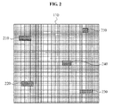
- FIG. 2 illustrates the encryption module 110 according to an embodiment of the present invention.
- the encryption module 110 may be connected to other components through the bus 102 in the encryption device 100.
- the encryption module 110 may include at least one encryption key module 210 220, 230, 240, and 250.
- the encryption key modules 210 220, 230, 240, and 250 may generate and/or store encryption keys to be used for executing an encryption algorithm, individually or jointly, and provide the encryption keys to the encryption module 110.
- a single encryption key module may be included in the encryption module 110.
- a plurality of encryption key modules may be included in the encryption module 110, as shown in FIG. 2 .
- At least a portion of the plurality of encryption key modules 210 220, 230, 240, and 250 may correspond to dummies not providing encryption keys in actual.
- An embodiment in which the encryption key modules 210 220, 230, 240, and 250 are implemented may include a case in which the encryption key modules 210 220, 230, 240, and 250 correspond to memory devices, and a case in which the encryption key modules 210 220, 230, 240, and 250 correspond to non-memory devices.
- An embodiment in which a portion of the encryption key modules 210 220, 230, 240, and 250 correspond to memory devices, and another portion of the encryption key modules 210 220, 230, 240, and 250 correspond to non-memory devices may also be possible.
- the present invention is not construed as being limited by a portion of the embodiments.
- pre-generated encryption keys of a form of a digital value may be simply stored in the encryption key modules 210 220, 230, 240, and 250 corresponding to the memory devices, and may be read for use, as necessary, in a process of executing an encryption algorithm by the encryption module 110.
- the encryption key modules 210 220, 230, 240, and 250 include non-memory devices
- at least a portion of the encryption key modules 210 220, 230, 240, and 250 may be implemented by physical unclonable functions (PUFs).
- PEFs physical unclonable functions
- the encryption key modules 210 220, 230, 240, and 250 include non-memory devices such as PUFs
- the PUFs may be implemented by intentionally violating a design rule in a semiconductor manufacturing process, or using a semiconductor manufacturing process variation.
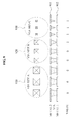
- FIG. 3 is a block diagram illustrating an exemplary configuration of the encryption module 110 according to an embodiment of the present invention.
- a single encryption key module 320 or a plurality of encryption key modules 320 may be physically included in the encryption module 110.
- an encryption key module selector 330 may select an encryption key module to provide an encryption key to be used for an encryption algorithm in actual.
- N denotes a natural number.
- Such a selection may correspond to index information of an encryption key module to be selected in actual, among indices identifying the encryption key modules 320, or may be predetermined by wiring in a process of designing and manufacturing the encryption key modules 320 along with the encryption module 110.
- an encryption unit 340 may execute an encryption algorithm using the encryption key to encrypt the input data, and the encrypted data may be transferred to other components via a data output unit 350 through the bus 102.
- the encryption key Since the encryption key is managed within the encryption module 110 autonomously, the encryption key may not be transferred to an external environment of the encryption module 110, or to the encryption module 110 from an external environment. Accordingly, a probability of success of physical attacks may decrease remarkably. In particular, a probability of success of a physical attack of probing the bus 102 may be extremely low.
- a PUF mentioned herein may generate an encryption key physically unclonable and unchanged once manufactured, at least in theory.
- FIGS. 4 through 8 may correspond to examples in which encryption key modules to generate encryption keys are implemented using a semiconductor process variation.
- FIGS. 9 through 13 correspond to examples in which encryption key modules to generate encryption keys are implemented by intentionally violating a design rule for designing a circuit.
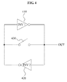
- FIG. 4 is an exemplary circuit diagram illustrating a concept of a unit cell constituting an encryption key module of a form of a PUF to generate an encryption key using a process variation according to an embodiment of the present invention.
- FIG. 4 a first inverter 410 and a second inverter 420 are shown.
- a semiconductor process variation may be caused by various reasons.
- a process variation may be caused by a parameter, for example, a threshold voltage, an index associated with an oxide thickness, an index associated with a doping concentration, a valid gate length, or the like.
- a semiconductor manufacturing process with a minor process variation may be regarded excellent.
- the process variation may be reducible, but not removable completely.
- the first inverter 410 may have a first logic threshold
- the second inverter 420 may have a second logic threshold.
- a logic threshold refers to a value of a voltage when an input voltage of an inverter is identical to an output voltage of the inverter.
- a logic threshold of an inverter device may be measured using a value of a voltage when an output terminal and an input terminal of an inverter being operated are shorted.
- Inverters manufactured by an identical process may be designed to have an identical logic threshold, in theory. However, as described above, due to a process variation in an actual manufacturing process, any two inverters may not have a perfectly identical logic threshold in actual.
- the first inverter 410 and the second inverter 420 may be manufactured by an identical process, and may have a difference between logic thresholds resulting from a process variation.
- the difference between the logic thresholds may vary depending on a process, however, for example, correspond to a size of about a few to tens of millivolts. Accordingly, the logic threshold of the first inverter 410 and the logic threshold of the second inverter 420 measured using a separate comparator circuit may be inaccurate due to an error in measurement.
- a greater logic threshold may be determined by comparing logic thresholds of two inverters relatively (autonomously without use of a separate comparator circuit).
- an output voltage of the first inverter 410 may be identical to a logic threshold of the first inverter 410 when an input terminal and an output terminal of the first inverter 410 are shorted.
- an output voltage of the second inverter 420 may be identical to a logic threshold of the second inverter 420 when an input terminal and an output terminal of the second inverter 420 are shorted.
- values of voltages of the two shorted nodes may be values between the logic threshold of the first inverter 410 and the logic threshold of the second inverter 420 (may not be an average value, hereinafter, the same shall apply).
- a value of an output voltage may be a value between the logic thresholds of the two inverters while the switch 430 is closed.
- a logical level of a value of a voltage of one of the first node and the second node may be "0", and a logical level of a value of a voltage of the other may be "1".
- a voltage of the first node may be higher than the logic threshold of the first inverter 410 while the switch 430 is closed such that the first node (an opposite node of an OUT node) and the second node (the OUT node) are shorted.
- the first inverter 410 may recognize a voltage of the first node (corresponding to the input terminal of the first inverter 410) as a high logical level, and make a voltage of the second node corresponding to the output terminal of the first inverter 410 be a low logical level.
- the second inverter 420 may recognize a voltage of the second node (corresponding to the input terminal of the second inverter 420) as a low logical level, and make a voltage of the first node corresponding to the output terminal of the second inverter 420 be a high logical level.
- the logical level of the voltage of the second terminal corresponding to the output terminal ("OUT") of FIG. 4 may be high.
- a voltage of the first node while the switch 430 is closed such that the first node and the second node are shorted may be lower than the logic threshold of the first inverter 410.
- the first inverter 410 may recognize a voltage of the first node (corresponding to the input terminal of the first inverter 410) as a low logical level, and make a voltage of the second node corresponding to the output terminal of the first inverter 410 be a high logical level.
- the second inverter 420 may recognize a voltage of the second node (corresponding to the input terminal of the second inverter 420) as a high logical level, and make a voltage of the first node corresponding to the output terminal of the second inverter 420 be a low logical level.
- the logical level of the voltage of the second terminal corresponding to the output terminal ("OUT") of FIG. 4 may be low.
- the logical level of the output terminal ("OUT") after the switch 430 is shorted-opened may be high (or "1"), or low (or "0").
- a greater value of logic thresholds of the first inverter 410 and the second inverter 420 manufactured by an identical manufacturing process may be determined at random. Probabilistically, a probability that one of two inverters has a logic threshold higher than a logic threshold of the other may be about 50%.
- a 1-bit digital value (a value having an identical probability of being “1” or being “0", however, difficult to change once manufactured) may be generated.
- FIG. 5 is a reference graph for understanding of the embodiment of FIG. 4 .
- the exemplary reference graph illustrates a voltage characteristic for a case in which the logic threshold of the first inverter 410 is lower than the logic threshold of the second inverter 420 of FIG. 4 .
- a curve 510 indicates a voltage characteristic of the first inverter 410
- a curve 520 indicates a voltage characteristic of the second inverter 420.
- the curve 510 and the curve 520 may be mostly identical, however, have a modest difference due to a process variation.
- the logic threshold V 1 of the first inverter 410 may be determined.
- the logic threshold V 2 of the second inverter 420 may be determined.
- V 1 is lower than V 2 . Accordingly, when the switch 430 of FIG. 4 is closed such that the first node and the second node are shorted (also referred to as "RESET"), voltages V RESET of the first node and the second node may correspond to values between V 1 and V 2 .
- the first inverter 410 may recognize the voltage V RESET of the first node as a high logical level, and make the voltage of the second node corresponding to the output terminal of the first inverter 410 be a low logical level.
- the second inverter 420 may recognize the voltage V RESET of the second node as a low logical level, and make the voltage of the first node corresponding to the output terminal of the second inverter 420 be a high logical level.
- the logical level of the voltage of the second terminal corresponding to the output terminal ("OUT") of FIG. 4 may be high.
- an encryption key may be generated using an N-bit digital value by integrating N unit cells.
- the encryption key modules 320 may be implemented using such a scheme.
- An encryption key module to generate an encryption key of a form of a digital value based on a difference between logic thresholds of inverter devices using a semiconductor process variation may be implemented by a configuration of FIG. 6 .
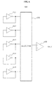
- FIG. 6 is a block diagram illustrating an exemplary implementation of an encryption key module 600 according to an embodiment of the present invention.
- the encryption key module 600 may include five inverters 611 through 615, a selector 620, and a comparator 630.
- the selector 620 may select two inverters from the five inverters of FIG. 6 .
- the inverter 612 and the inverter 613 may be selected.
- the comparator 630 may compare a logic threshold of the inverter 612 to a logic threshold of the inverter 613, and provide an output voltage to an OUT terminal based on a result of the comparing.
- a 1-bit digital value may be generated based on a logical level of the output voltage of the OUT terminal.
- the comparator 630 may generate a 1-bit digital value again.
- the selector 620 selects two inverters from the five inverters 611 through 615, and the comparator 630 generates a digital value by comparing logic thresholds of the two selected inverters, a digital value of a maximum of 10 bits may be obtained.
- the present invention is not limited thereto. Various changes may be made in view of an area of a circuit, a number of bits in a digital value to be generated, and the like.
- a plurality of inverters and the single comparator 630 are connected through the selector 620.
- a single comparator may make a pair with two inverters to generate an N-bit digital value.
- the encryption key module to generate an encryption key of a form of a digital value based on a difference between logic thresholds of inverter devices using a semiconductor process variation may also be implemented by a configuration of FIG. 7 .
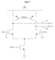
- FIG. 7 illustrates a unit cell 700 of an encryption key module to generate a digital value using a process variation of a differential amplifier according to an embodiment of the present invention.
- the unit cell 700 may correspond to a circuit of a differential amplifier.
- the unit cell corresponding to the circuit of the differential amplifier including at least one device of a transistor and a resistor may amplify a difference between a voltage of a first input terminal 711 and a voltage of a second input terminal 712, and provide the amplified difference as a difference between a voltage of a first output terminal 721 and a voltage of a second output terminal 722.
- a value of an output voltage corresponding to the difference of the voltage of the first output terminal 721 and the voltage of the second output terminal 722 may be "0", in theory.
- the voltage of the first output terminal 721 may not be completely identical to the voltage of the second output terminal 722.
- a 1-bit digital value may be generated.
- each of the N unit cells may corresponding to differential amplifier 700, an encryption key may be provided in a form of an N-bit digital value, and an encryption key module according to an embodiment of the present invention may be implemented.
- an implementation is illustrated in FIG. 8 .
- FIG. 8 illustrates an exemplary circuit diagram in which an encryption key module 800 is implemented according to an embodiment of the present invention.
- the encryption key module 800 may include six differential amplifiers 811 through 816, a selector 820 to select one from the six differential amplifiers, and a comparator 830 to compare two output voltages of the differential amplifier selected by the selector 820 to generate a 1-bit digital value.
- all input terminals of the six differential amplifiers 811 through 816 may be shorted, and may have an identical voltage.
- the selector 820 may include a 6:1 multiplexer (MUX) device.
- MUX 6:1 multiplexer
- the present embodiment may be an example for implementation of the present invention, and the present invention is not limited to a specific embodiment.
- the selector 820 may include another device, other than the MUX device.
- the 6:1 MUX device may output, to two output terminals, output voltages of the six differential amplifiers through twelve input terminals.
- the two output terminals may be connected to two input terminals of the comparator 830.
- the encryption key module 800 may generate an encryption key corresponding to a 6-bit digital value.
- FIG. 9 is a conceptual diagram illustrating a principle of generating an encryption key module by intentionally violating a semiconductor design rule according to an embodiment of the present invention.
- a contact or a via may be designed to connect conductive layers, and a size of the contact or the via may be determined for the conductive layers to be shorted. In a general design rule, a minimum size of a contact or a via may be determined to guarantee that conductive layers are shorted.
- a portion of contacts or vias may short conductive layers, and another portion of the contacts or the vias may not short the conductive layers. Whether the contacts or the vias short the conductive layers may be determined, probabilistically.
- vias may be formed between a first metal layer 902 and a second metal layer 901 in a semiconductor manufacturing process.
- all of the vias short the first metal layer 902 and the second metal layer 901, and whether the vias short the first metal layer 902 and the second metal layer 901 may be expressed by a digital value "0".
- a portion of the vias short the first metal layer 902 and the second metal layer 901, and another portion of the vias do not short the first metal layer 902 and the second metal layer 901.
- sizes of vias may be set for a portion of the vias to short the first metal layer 902 and the second metal layer 901, and another portion of the vias not to short the first metal layer 902 and the second metal layer 901, as shown in the group 920.
- a design rule associated with a size of a via may vary depending on a semiconductor manufacturing process. For example, when a size of a via complying a design rule is set to 0.25 micrometers ( ⁇ m) in a process of manufacturing a complementary metal-oxide-semiconductor (CMOS) of 0.18 ⁇ m, in an implementation of an encryption key module according to an embodiment of the present invention, the design rule may be violated intentionally to set the size of the via to 0.19 ⁇ m, whereby whether the via short metal layers may be distributed probabilistically.
- CMOS complementary metal-oxide-semiconductor
- the distribution of the probability regarding whether the via short the metal layers may be set to have a short probability of 50%, for optimal efficiency.
- the size of the via may be set for the distribution of the probability to be close to 50% to the maximum.
- the size of the via may be determined by an experiment according to a process.
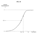
- FIG. 10 is a graph illustrating a configuration of an encryption key module implemented by intentionally violating a semiconductor design rule according to an embodiment of the present invention.
- Sd denotes a size of a via according to a design rule, and may correspond to a value sufficiently guaranteeing that the metal layers are shorted.
- Sm denotes a size of a via with which a probability that the metal layers are shorted may correspond to "0.5", in theory. As described above, the value may be changed depending on a process, and a most similar value may be found by an experiment. However, an accurate value of Sm may be difficult to find.
- whether the metal layers are shorted may be set within a range between Sx1 and Sx2 (although not shown separately, denoting a region having a predetermined margin based on Sx) having a predetermined tolerance based on 0.5, by a detailed experiment.
- encryption key modules may be implemented by intentionally violating a design rule associated with a gap between conductive layers.
- FIG. 11 is a conceptual diagram illustrating a process of generating an encryption key module by adjusting a gap between conductive layers according to an embodiment of the present invention.
- gaps between metal lines may be set to short the metal lines probabilistically, for a portion of the metal lines to be shorted and another portion of the metal lines not to be shorted, as shown in a group 1120.
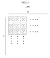
- FIG. 12 is a conceptual diagram illustrating an exemplary structure of an array of vias or contacts formed on a semiconductor layer to implement an encryption key module 1200 according to an embodiment of the present invention.
- M vias in width and N vias in length, a total of M x N vias, may be formed between metal layers laminated on a semiconductor substrate.
- M and N denote natural numbers.
- the encryption key module 1200 may generate and provide an encryption key of M x N bits, based on whether each of the M x N vias shorts the metal layers (a digital value "0"), or does not short the metal layers (a digital value "1").
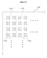
- FIG. 13 is a conceptual diagram illustrating a process of post-processing a digital value generated in the embodiment of FIG. 12 for balancing of "0" and "1", rather than using the original digital value as an encryption key, according to an embodiment of the present invention.
- an M x N-bit digital value generated by the encryption key module 1200 may be divided based on k predetermined units.
- k denotes a natural number.
- the division shown in FIG. 13 may be provided as an example for ease of description. In an actual implementation, a method of dividing flip-flops or registers in the encryption key module 1200, and the like may be possible.
- four digital values may be classified as a single group.
- the encryption key module 1200 may compare a size of a 4-bit digital value generated by a group 1310 to a size of a 4-bit digital value generated by a group 1320. When the 4-bit digital value of the group 1310 is greater than the 4-bit digital value of the group 1320, digital values representing the group 1310 and the group 1320 may be determined to be "1".
- the digital values representing the group 1310 and the group 1320 may be determined to be "0".
- digital values representing groups may be determined by comparing numbers of 1-bit digital values of the groups.
- the method according to the above-described embodiments of the present invention may be recorded in computer-readable media including program instructions to implement various operations embodied by a computer.
- the media may also include, alone or in combination with the program instructions, data files, data structures, and the like.
- Examples of computer-readable media include magnetic media such as hard disks, floppy disks, and magnetic tape; optical media such as CD ROM discs and DVDs; magneto-optical media such as floptical discs; and hardware devices that are specially configured to store and perform program instructions, such as read-only memory (ROM), random access memory (RAM), flash memory, and the like.
- Examples of program instructions include both machine code, such as produced by a compiler, and files containing higher level code that may be executed by the computer using an interpreter.
- the described hardware devices may be configured to act as one or more software modules in order to perform the operations of the above-described exemplary embodiments of the present invention, or vice versa.
Landscapes
- Engineering & Computer Science (AREA)
- Computer Security & Cryptography (AREA)
- Theoretical Computer Science (AREA)
- Physics & Mathematics (AREA)
- Computer Hardware Design (AREA)
- Computer Networks & Wireless Communication (AREA)
- Signal Processing (AREA)
- General Engineering & Computer Science (AREA)
- General Physics & Mathematics (AREA)
- Software Systems (AREA)
- Mathematical Physics (AREA)
- Semiconductor Integrated Circuits (AREA)
- Storage Device Security (AREA)
Applications Claiming Priority (2)
| Application Number | Priority Date | Filing Date | Title |
|---|---|---|---|
| KR1020110013269A KR101118826B1 (ko) | 2011-02-15 | 2011-02-15 | 물리적 공격을 방어하는 암호화 장치 및 암호화 방법 |
| PCT/KR2011/001376 WO2012111872A1 (fr) | 2011-02-15 | 2011-02-28 | Dispositif de chiffrement et procédé de défense contre une attaque physique |
Publications (3)
| Publication Number | Publication Date |
|---|---|
| EP2677452A1 true EP2677452A1 (fr) | 2013-12-25 |
| EP2677452A4 EP2677452A4 (fr) | 2014-08-06 |
| EP2677452B1 EP2677452B1 (fr) | 2018-08-22 |
Family
ID=46141374
Family Applications (1)
| Application Number | Title | Priority Date | Filing Date |
|---|---|---|---|
| EP11858891.2A Active EP2677452B1 (fr) | 2011-02-15 | 2011-02-28 | Dispositif de chiffrement et procédé de défense contre une attaque physique |
Country Status (7)
| Country | Link |
|---|---|
| US (3) | US9014371B2 (fr) |
| EP (1) | EP2677452B1 (fr) |
| JP (2) | JP2014506095A (fr) |
| KR (1) | KR101118826B1 (fr) |
| CN (2) | CN103621006B (fr) |
| ES (1) | ES2685758T3 (fr) |
| WO (1) | WO2012111872A1 (fr) |
Cited By (3)
| Publication number | Priority date | Publication date | Assignee | Title |
|---|---|---|---|---|
| US9076003B2 (en) | 2013-08-20 | 2015-07-07 | Janus Technologies, Inc. | Method and apparatus for transparently encrypting and decrypting computer interface data |
| EP3043282A4 (fr) * | 2013-09-03 | 2017-01-18 | ICTK Co. Ltd. | Dispositif et procédé permettant de générer une clé d'identification |
| EP3043281A4 (fr) * | 2013-09-06 | 2017-02-08 | ICTK Co. Ltd. | Dispositif et procédé permettant de générer une clé d'identification |
Families Citing this family (27)
| Publication number | Priority date | Publication date | Assignee | Title |
|---|---|---|---|---|
| US20150071434A1 (en) * | 2011-06-07 | 2015-03-12 | Static Control Components, Inc. | Secure Semiconductor Device Having Features to Prevent Reverse Engineering |
| KR102178386B1 (ko) | 2013-07-26 | 2020-11-12 | 주식회사 아이씨티케이 홀딩스 | 랜덤성 테스트 장치 및 방법 |
| KR101489091B1 (ko) * | 2013-09-30 | 2015-02-04 | (주) 아이씨티케이 | 반도체 공정을 이용한 식별키 생성 장치 및 방법 |
| KR101495448B1 (ko) | 2013-10-29 | 2015-02-26 | (주) 아이씨티케이 | 사용자 인증을 위한 ic 칩 및 인증 방법 |
| KR102201642B1 (ko) | 2014-11-28 | 2021-01-13 | 삼성전자주식회사 | Puf 회로 및 그것의 키 등록 방법 |
| KR101801547B1 (ko) | 2015-08-25 | 2017-11-27 | 한국과학기술원 | 물리적, 영구적 파괴를 이용한 하드웨어 기반의 보안 장치 및 이를 이용한 보안 방법 |
| US20170077046A1 (en) * | 2015-09-11 | 2017-03-16 | The Regents Of The University Of California | Physical unclonable functions through locally enhanced defectivity |
| WO2017048257A1 (fr) * | 2015-09-17 | 2017-03-23 | Hewlett Packard Enterprise Development Lp | Occultation d'un signal de cache |
| CN108701193B (zh) | 2016-02-12 | 2022-08-30 | 汉阳大学校产学协力团 | 安全半导体芯片及其工作方法 |
| WO2017138799A1 (fr) * | 2016-02-12 | 2017-08-17 | 한양대학교 산학협력단 | Dispositif matériel et procédé d'autorisation associé |
| WO2017138797A1 (fr) * | 2016-02-12 | 2017-08-17 | 한양대학교 산학협력단 | Système sur puce de sécurité |
| CN105790933A (zh) * | 2016-03-03 | 2016-07-20 | 山东超越数控电子有限公司 | 一种自动识别的光模块加密方法 |
| JP6471130B2 (ja) | 2016-09-20 | 2019-02-13 | ウィンボンド エレクトロニクス コーポレーション | 半導体装置およびセキュリティシステム |
| KR102071402B1 (ko) * | 2016-11-01 | 2020-03-03 | 한국전자통신연구원 | 사물인터넷 환경 키 관리 서비스 제공 장치 |
| KR102050021B1 (ko) * | 2017-04-27 | 2019-11-28 | 김태욱 | 식별키 유용성 판별장치 |
| KR102071937B1 (ko) * | 2017-04-27 | 2020-01-31 | 김태욱 | 식별키 생성장치 및 식별키 생성방법 |
| DE102018123103A1 (de) * | 2017-10-13 | 2019-04-18 | Samsung Electronics Co., Ltd. | Halbleitervorrichtung, die Sicherheitsschlüssel erzeugt, Verfahren zum Erzeugen eines Sicherheitsschlüssels und Verfahren zum Registrieren des Sicherheitsschlüssels |
| US11108572B2 (en) * | 2018-10-11 | 2021-08-31 | Taiwan Semiconductor Manufacturing Company, Ltd. | Physically unclonable function device with a load circuit to generate bias to sense amplifier |
| KR102244382B1 (ko) | 2019-06-13 | 2021-04-26 | 숭실대학교산학협력단 | Wave-chaos 기반 무선 신호 전송의 물리적 암호화 시스템 |
| KR102146132B1 (ko) * | 2019-08-08 | 2020-08-20 | 주식회사 페이콕 | 보안 디바이스 및 방법 |
| US11282799B2 (en) | 2020-01-14 | 2022-03-22 | United Microelectronics Corp. | Device for generating security key and manufacturing method thereof |
| US11127480B1 (en) * | 2020-06-30 | 2021-09-21 | Dell Products L.P. | System and method for short circuit detection |
| CN112733209B (zh) * | 2021-01-19 | 2023-08-08 | 贵州黔龙图视科技有限公司 | 一种低成本硬件加密方法及装置 |
| KR20220155684A (ko) | 2021-05-17 | 2022-11-24 | 삼성전자주식회사 | Crum 칩 및 스마트 카드 |
| US11574079B2 (en) * | 2021-05-27 | 2023-02-07 | Nuvoton Technology Corporation | Multi-stage provisioning of secret data |
| US11791290B2 (en) | 2021-06-29 | 2023-10-17 | International Business Machines Corporation | Physical unclonable function for secure integrated hardware systems |
| CN115130152B (zh) * | 2022-09-01 | 2022-11-18 | 北京紫光青藤微系统有限公司 | 一种物理不可克隆函数的生成方法及装置 |
Citations (2)
| Publication number | Priority date | Publication date | Assignee | Title |
|---|---|---|---|---|
| US20080044010A1 (en) * | 2005-07-12 | 2008-02-21 | Ihor Vasyltasov | Cryptographic system and method for encrypting input data |
| US20080285745A1 (en) * | 2004-03-29 | 2008-11-20 | Stmicroelectronics S.A. | Processor for Executing an Aes-Type Algorithm |
Family Cites Families (32)
| Publication number | Priority date | Publication date | Assignee | Title |
|---|---|---|---|---|
| US5559889A (en) * | 1995-03-31 | 1996-09-24 | International Business Machines Corporation | System and methods for data encryption using public key cryptography |
| JP3673015B2 (ja) | 1996-04-26 | 2005-07-20 | 沖電気工業株式会社 | 半導体装置における周辺デバイス識別方法 |
| US5802592A (en) | 1996-05-31 | 1998-09-01 | International Business Machines Corporation | System and method for protecting integrity of alterable ROM using digital signatures |
| JPH10116326A (ja) * | 1996-10-11 | 1998-05-06 | Secom Co Ltd | Icカード用暗号化装置 |
| US5990701A (en) | 1997-06-25 | 1999-11-23 | Sun Microsystems, Inc. | Method of broadly distributing termination for buses using switched terminators |
| US6118279A (en) | 1997-07-30 | 2000-09-12 | Candescent Technologies Corporation | Magnetic detection of short circuit defects in plate structure |
| JP2000122931A (ja) | 1998-10-15 | 2000-04-28 | Toshiba Corp | デジタル集積回路 |
| US6555204B1 (en) | 2000-03-14 | 2003-04-29 | International Business Machines Corporation | Method of preventing bridging between polycrystalline micro-scale features |
| WO2002050910A1 (fr) | 2000-12-01 | 2002-06-27 | Hitachi, Ltd | Procede d'identification de dispositif de circuit integre semi-conducteur, procede de production de dispositif de circuit integre semi-conducteur et dispositif correspondant |
| US7085386B2 (en) | 2001-12-07 | 2006-08-01 | Activcard | System and method for secure replacement of high level cryptographic keys in a personal security device |
| US7266661B2 (en) * | 2004-05-27 | 2007-09-04 | Silverbrook Research Pty Ltd | Method of storing bit-pattern in plural devices |
| JP2006108903A (ja) * | 2004-10-01 | 2006-04-20 | Hiromi Fukaya | 暗号化データ配布方法、暗号化装置、復号化装置、暗号化プログラム及び復号化プログラム |
| US7564345B2 (en) * | 2004-11-12 | 2009-07-21 | Verayo, Inc. | Volatile device keys and applications thereof |
| JP4524176B2 (ja) * | 2004-12-17 | 2010-08-11 | パナソニック株式会社 | 電子デバイスの製造方法 |
| EP1961140A4 (fr) * | 2005-12-14 | 2013-02-27 | Nds Ltd | Procede et systeme pour l'usage de criptage de chiffrement par bloc |
| ATE504884T1 (de) | 2006-01-24 | 2011-04-15 | Verayo Inc | Signalgeneratorbasierte vorrichtungssicherheit |
| US8036379B2 (en) * | 2006-03-15 | 2011-10-11 | Microsoft Corporation | Cryptographic processing |
| CN101421792B (zh) | 2006-04-13 | 2015-09-23 | Nxp股份有限公司 | 半导体器件标识符产生方法以及半导体器件 |
| CN100568393C (zh) * | 2006-06-14 | 2009-12-09 | 国际商业机器公司 | 数据存储装置、数据存储方法以及数据读取方法 |
| JP5113074B2 (ja) * | 2006-11-06 | 2013-01-09 | パナソニック株式会社 | 情報セキュリティ装置 |
| US20110215829A1 (en) | 2007-08-22 | 2011-09-08 | Intrinsic Id B.V. | Identification of devices using physically unclonable functions |
| KR100969961B1 (ko) * | 2007-12-20 | 2010-07-15 | 한국전자통신연구원 | 블록 암호 아리아의 치환 연산 장치 및 방법 |
| CN101498772B (zh) | 2008-01-29 | 2012-07-18 | 西门子(中国)有限公司 | 磁共振成像系统中接收线圈的识别码电路 |
| US7991154B2 (en) * | 2008-05-14 | 2011-08-02 | Univeristy of Castilla-La Mancha | Exponentiation method using multibase number representation |
| KR100960113B1 (ko) * | 2008-09-19 | 2010-05-27 | 한국전자통신연구원 | 고속처리 가능한 아리아 암복호화 장치 |
| US8699714B2 (en) | 2008-11-17 | 2014-04-15 | Intrinsic Id B.V. | Distributed PUF |
| US8051097B2 (en) * | 2008-12-15 | 2011-11-01 | Apple Inc. | System and method for authentication using a shared table and sorting exponentiation |
| KR100926214B1 (ko) | 2009-04-23 | 2009-11-09 | 한양대학교 산학협력단 | 공정편차를 이용한 디지털 값 생성 장치 및 방법 |
| JP2011010218A (ja) * | 2009-06-29 | 2011-01-13 | Toshiba Corp | 携帯可能電子装置、及び携帯可能電子装置の制御方法 |
| US20110080715A1 (en) | 2009-10-07 | 2011-04-07 | Castles Technology Co., Ltd. | Protective structure of electronic component |
| US8127151B2 (en) | 2009-10-13 | 2012-02-28 | Lockheed Martin Corporation | Hardware-based key generation and recovery |
| KR101139630B1 (ko) | 2010-12-09 | 2012-05-30 | 한양대학교 산학협력단 | 식별키 생성 장치 및 방법 |
-
2011
- 2011-02-15 KR KR1020110013269A patent/KR101118826B1/ko active IP Right Grant
- 2011-02-28 CN CN201180070008.XA patent/CN103621006B/zh active Active
- 2011-02-28 CN CN201610621693.5A patent/CN106295408B/zh active Active
- 2011-02-28 ES ES11858891.2T patent/ES2685758T3/es active Active
- 2011-02-28 EP EP11858891.2A patent/EP2677452B1/fr active Active
- 2011-02-28 WO PCT/KR2011/001376 patent/WO2012111872A1/fr active Application Filing
- 2011-02-28 US US13/985,765 patent/US9014371B2/en active Active
- 2011-02-28 JP JP2013554380A patent/JP2014506095A/ja active Pending
-
2015
- 2015-03-23 US US14/665,599 patent/US9397826B2/en active Active
- 2015-09-28 JP JP2015189092A patent/JP2016021772A/ja active Pending
-
2016
- 2016-06-20 US US15/187,630 patent/US20160301528A1/en not_active Abandoned
Patent Citations (2)
| Publication number | Priority date | Publication date | Assignee | Title |
|---|---|---|---|---|
| US20080285745A1 (en) * | 2004-03-29 | 2008-11-20 | Stmicroelectronics S.A. | Processor for Executing an Aes-Type Algorithm |
| US20080044010A1 (en) * | 2005-07-12 | 2008-02-21 | Ihor Vasyltasov | Cryptographic system and method for encrypting input data |
Non-Patent Citations (1)
| Title |
|---|
| See also references of WO2012111872A1 * |
Cited By (4)
| Publication number | Priority date | Publication date | Assignee | Title |
|---|---|---|---|---|
| US9076003B2 (en) | 2013-08-20 | 2015-07-07 | Janus Technologies, Inc. | Method and apparatus for transparently encrypting and decrypting computer interface data |
| EP3043282A4 (fr) * | 2013-09-03 | 2017-01-18 | ICTK Co. Ltd. | Dispositif et procédé permettant de générer une clé d'identification |
| US9859228B2 (en) | 2013-09-03 | 2018-01-02 | Ictk Co., Ltd. | Device and method for generating identification key |
| EP3043281A4 (fr) * | 2013-09-06 | 2017-02-08 | ICTK Co. Ltd. | Dispositif et procédé permettant de générer une clé d'identification |
Also Published As
| Publication number | Publication date |
|---|---|
| JP2014506095A (ja) | 2014-03-06 |
| CN103621006B (zh) | 2016-09-07 |
| CN106295408A (zh) | 2017-01-04 |
| US20160301528A1 (en) | 2016-10-13 |
| JP2016021772A (ja) | 2016-02-04 |
| EP2677452A4 (fr) | 2014-08-06 |
| US20130322624A1 (en) | 2013-12-05 |
| WO2012111872A1 (fr) | 2012-08-23 |
| CN106295408B (zh) | 2020-06-02 |
| US9397826B2 (en) | 2016-07-19 |
| KR101118826B1 (ko) | 2012-04-20 |
| CN103621006A (zh) | 2014-03-05 |
| EP2677452B1 (fr) | 2018-08-22 |
| US20150195085A1 (en) | 2015-07-09 |
| ES2685758T3 (es) | 2018-10-11 |
| US9014371B2 (en) | 2015-04-21 |
Similar Documents
| Publication | Publication Date | Title |
|---|---|---|
| US9397826B2 (en) | Encryption device and method for defending a physical attack | |
| US20200364374A1 (en) | Apparatus and method for generating identification key | |
| Joshi et al. | Everything you wanted to know about PUFs | |
| US8749265B2 (en) | Semiconductor chip and method for generating digital value using process variation | |
| KR101663341B1 (ko) | 식별키 생성 장치 및 방법 | |
| CN104978499A (zh) | 用于制造数字电路的方法和数字电路 | |
| Koeberl et al. | Evaluation of a PUF Device Authentication Scheme on a Discrete 0.13 um SRAM | |
| Cambou | Enhancing secure elements—technology and architecture | |
| Komurcu et al. | Enhanced challenge-response set and secure usage scenarios for ordering based RO-PUFs | |
| Maes et al. | Process variations for security: Pufs |
Legal Events
| Date | Code | Title | Description |
|---|---|---|---|
| PUAI | Public reference made under article 153(3) epc to a published international application that has entered the european phase |
Free format text: ORIGINAL CODE: 0009012 |
|
| 17P | Request for examination filed |
Effective date: 20130913 |
|
| AK | Designated contracting states |
Kind code of ref document: A1 Designated state(s): AL AT BE BG CH CY CZ DE DK EE ES FI FR GB GR HR HU IE IS IT LI LT LU LV MC MK MT NL NO PL PT RO RS SE SI SK SM TR |
|
| AX | Request for extension of the european patent |
Extension state: BA ME |
|
| A4 | Supplementary search report drawn up and despatched |
Effective date: 20140708 |
|
| RIC1 | Information provided on ipc code assigned before grant |
Ipc: G06F 21/71 20130101AFI20140702BHEP Ipc: H04L 9/28 20060101ALI20140702BHEP Ipc: G06F 21/00 20130101ALI20140702BHEP |
|
| RAP1 | Party data changed (applicant data changed or rights of an application transferred) |
Owner name: ICTK CO., LTD. |
|
| 17Q | First examination report despatched |
Effective date: 20160310 |
|
| STAA | Information on the status of an ep patent application or granted ep patent |
Free format text: STATUS: EXAMINATION IS IN PROGRESS |
|
| REG | Reference to a national code |
Ref country code: DE Ref legal event code: R079 Ref document number: 602011051421 Country of ref document: DE Free format text: PREVIOUS MAIN CLASS: G06F0021240000 Ipc: G06F0021720000 |
|
| GRAP | Despatch of communication of intention to grant a patent |
Free format text: ORIGINAL CODE: EPIDOSNIGR1 |
|
| STAA | Information on the status of an ep patent application or granted ep patent |
Free format text: STATUS: GRANT OF PATENT IS INTENDED |
|
| RIC1 | Information provided on ipc code assigned before grant |
Ipc: H04L 9/00 20060101ALI20180209BHEP Ipc: G06F 21/72 20130101AFI20180209BHEP |
|
| INTG | Intention to grant announced |
Effective date: 20180305 |
|
| GRAS | Grant fee paid |
Free format text: ORIGINAL CODE: EPIDOSNIGR3 |
|
| GRAA | (expected) grant |
Free format text: ORIGINAL CODE: 0009210 |
|
| STAA | Information on the status of an ep patent application or granted ep patent |
Free format text: STATUS: THE PATENT HAS BEEN GRANTED |
|
| AK | Designated contracting states |
Kind code of ref document: B1 Designated state(s): AL AT BE BG CH CY CZ DE DK EE ES FI FR GB GR HR HU IE IS IT LI LT LU LV MC MK MT NL NO PL PT RO RS SE SI SK SM TR |
|
| AX | Request for extension of the european patent |
Extension state: BA ME |
|
| REG | Reference to a national code |
Ref country code: GB Ref legal event code: FG4D |
|
| REG | Reference to a national code |
Ref country code: CH Ref legal event code: EP |
|
| REG | Reference to a national code |
Ref country code: AT Ref legal event code: REF Ref document number: 1033323 Country of ref document: AT Kind code of ref document: T Effective date: 20180915 |
|
| REG | Reference to a national code |
Ref country code: IE Ref legal event code: FG4D Ref country code: NL Ref legal event code: FP |
|
| REG | Reference to a national code |
Ref country code: DE Ref legal event code: R096 Ref document number: 602011051421 Country of ref document: DE |
|
| REG | Reference to a national code |
Ref country code: ES Ref legal event code: FG2A Ref document number: 2685758 Country of ref document: ES Kind code of ref document: T3 Effective date: 20181011 |
|
| REG | Reference to a national code |
Ref country code: DE Ref legal event code: R082 Ref document number: 602011051421 Country of ref document: DE Representative=s name: HERNANDEZ, YORCK, DIPL.-ING., DE Ref country code: DE Ref legal event code: R081 Ref document number: 602011051421 Country of ref document: DE Owner name: ICTK HOLDINGS CO., LTD., SEONGNAM-SI, KR Free format text: FORMER OWNER: ICTK CO., LTD., SEOUL, KR |
|
| REG | Reference to a national code |
Ref country code: CH Ref legal event code: NV Representative=s name: TR-IP CONSULTING LLC, CH |
|
| RAP2 | Party data changed (patent owner data changed or rights of a patent transferred) |
Owner name: ICTK HOLDINGS CO., LTD. |
|
| REG | Reference to a national code |
Ref country code: BE Ref legal event code: PD Owner name: ICTK HOLDINGS CO., LTD.; KR Free format text: DETAILS ASSIGNMENT: CHANGE OF OWNER(S), CESSION; FORMER OWNER NAME: ICTK CO., LTD. Effective date: 20181116 |
|
| REG | Reference to a national code |
Ref country code: LT Ref legal event code: MG4D |
|
| REG | Reference to a national code |
Ref country code: NL Ref legal event code: PD Owner name: ICTK HOLDINGS CO., LTD.; KR Free format text: DETAILS ASSIGNMENT: CHANGE OF OWNER(S), ASSIGNMENT; FORMER OWNER NAME: ICTK CO., LTD. Effective date: 20181120 |
|
| PG25 | Lapsed in a contracting state [announced via postgrant information from national office to epo] |
Ref country code: FI Free format text: LAPSE BECAUSE OF FAILURE TO SUBMIT A TRANSLATION OF THE DESCRIPTION OR TO PAY THE FEE WITHIN THE PRESCRIBED TIME-LIMIT Effective date: 20180822 Ref country code: RS Free format text: LAPSE BECAUSE OF FAILURE TO SUBMIT A TRANSLATION OF THE DESCRIPTION OR TO PAY THE FEE WITHIN THE PRESCRIBED TIME-LIMIT Effective date: 20180822 Ref country code: IS Free format text: LAPSE BECAUSE OF FAILURE TO SUBMIT A TRANSLATION OF THE DESCRIPTION OR TO PAY THE FEE WITHIN THE PRESCRIBED TIME-LIMIT Effective date: 20181222 Ref country code: GR Free format text: LAPSE BECAUSE OF FAILURE TO SUBMIT A TRANSLATION OF THE DESCRIPTION OR TO PAY THE FEE WITHIN THE PRESCRIBED TIME-LIMIT Effective date: 20181123 Ref country code: NO Free format text: LAPSE BECAUSE OF FAILURE TO SUBMIT A TRANSLATION OF THE DESCRIPTION OR TO PAY THE FEE WITHIN THE PRESCRIBED TIME-LIMIT Effective date: 20181122 Ref country code: SE Free format text: LAPSE BECAUSE OF FAILURE TO SUBMIT A TRANSLATION OF THE DESCRIPTION OR TO PAY THE FEE WITHIN THE PRESCRIBED TIME-LIMIT Effective date: 20180822 Ref country code: BG Free format text: LAPSE BECAUSE OF FAILURE TO SUBMIT A TRANSLATION OF THE DESCRIPTION OR TO PAY THE FEE WITHIN THE PRESCRIBED TIME-LIMIT Effective date: 20181122 Ref country code: LT Free format text: LAPSE BECAUSE OF FAILURE TO SUBMIT A TRANSLATION OF THE DESCRIPTION OR TO PAY THE FEE WITHIN THE PRESCRIBED TIME-LIMIT Effective date: 20180822 |
|
| REG | Reference to a national code |
Ref country code: AT Ref legal event code: MK05 Ref document number: 1033323 Country of ref document: AT Kind code of ref document: T Effective date: 20180822 |
|
| PG25 | Lapsed in a contracting state [announced via postgrant information from national office to epo] |
Ref country code: AL Free format text: LAPSE BECAUSE OF FAILURE TO SUBMIT A TRANSLATION OF THE DESCRIPTION OR TO PAY THE FEE WITHIN THE PRESCRIBED TIME-LIMIT Effective date: 20180822 Ref country code: LV Free format text: LAPSE BECAUSE OF FAILURE TO SUBMIT A TRANSLATION OF THE DESCRIPTION OR TO PAY THE FEE WITHIN THE PRESCRIBED TIME-LIMIT Effective date: 20180822 Ref country code: HR Free format text: LAPSE BECAUSE OF FAILURE TO SUBMIT A TRANSLATION OF THE DESCRIPTION OR TO PAY THE FEE WITHIN THE PRESCRIBED TIME-LIMIT Effective date: 20180822 |
|
| PG25 | Lapsed in a contracting state [announced via postgrant information from national office to epo] |
Ref country code: PL Free format text: LAPSE BECAUSE OF FAILURE TO SUBMIT A TRANSLATION OF THE DESCRIPTION OR TO PAY THE FEE WITHIN THE PRESCRIBED TIME-LIMIT Effective date: 20180822 Ref country code: AT Free format text: LAPSE BECAUSE OF FAILURE TO SUBMIT A TRANSLATION OF THE DESCRIPTION OR TO PAY THE FEE WITHIN THE PRESCRIBED TIME-LIMIT Effective date: 20180822 Ref country code: CZ Free format text: LAPSE BECAUSE OF FAILURE TO SUBMIT A TRANSLATION OF THE DESCRIPTION OR TO PAY THE FEE WITHIN THE PRESCRIBED TIME-LIMIT Effective date: 20180822 Ref country code: RO Free format text: LAPSE BECAUSE OF FAILURE TO SUBMIT A TRANSLATION OF THE DESCRIPTION OR TO PAY THE FEE WITHIN THE PRESCRIBED TIME-LIMIT Effective date: 20180822 Ref country code: EE Free format text: LAPSE BECAUSE OF FAILURE TO SUBMIT A TRANSLATION OF THE DESCRIPTION OR TO PAY THE FEE WITHIN THE PRESCRIBED TIME-LIMIT Effective date: 20180822 |
|
| REG | Reference to a national code |
Ref country code: DE Ref legal event code: R097 Ref document number: 602011051421 Country of ref document: DE |
|
| PG25 | Lapsed in a contracting state [announced via postgrant information from national office to epo] |
Ref country code: DK Free format text: LAPSE BECAUSE OF FAILURE TO SUBMIT A TRANSLATION OF THE DESCRIPTION OR TO PAY THE FEE WITHIN THE PRESCRIBED TIME-LIMIT Effective date: 20180822 Ref country code: SM Free format text: LAPSE BECAUSE OF FAILURE TO SUBMIT A TRANSLATION OF THE DESCRIPTION OR TO PAY THE FEE WITHIN THE PRESCRIBED TIME-LIMIT Effective date: 20180822 Ref country code: SK Free format text: LAPSE BECAUSE OF FAILURE TO SUBMIT A TRANSLATION OF THE DESCRIPTION OR TO PAY THE FEE WITHIN THE PRESCRIBED TIME-LIMIT Effective date: 20180822 |
|
| PLBE | No opposition filed within time limit |
Free format text: ORIGINAL CODE: 0009261 |
|
| STAA | Information on the status of an ep patent application or granted ep patent |
Free format text: STATUS: NO OPPOSITION FILED WITHIN TIME LIMIT |
|
| 26N | No opposition filed |
Effective date: 20190523 |
|
| REG | Reference to a national code |
Ref country code: GB Ref legal event code: 732E Free format text: REGISTERED BETWEEN 20190801 AND 20190807 |
|
| PG25 | Lapsed in a contracting state [announced via postgrant information from national office to epo] |
Ref country code: SI Free format text: LAPSE BECAUSE OF FAILURE TO SUBMIT A TRANSLATION OF THE DESCRIPTION OR TO PAY THE FEE WITHIN THE PRESCRIBED TIME-LIMIT Effective date: 20180822 |
|
| PG25 | Lapsed in a contracting state [announced via postgrant information from national office to epo] |
Ref country code: MC Free format text: LAPSE BECAUSE OF FAILURE TO SUBMIT A TRANSLATION OF THE DESCRIPTION OR TO PAY THE FEE WITHIN THE PRESCRIBED TIME-LIMIT Effective date: 20180822 |
|
| REG | Reference to a national code |
Ref country code: IE Ref legal event code: MM4A |
|
| PG25 | Lapsed in a contracting state [announced via postgrant information from national office to epo] |
Ref country code: IE Free format text: LAPSE BECAUSE OF NON-PAYMENT OF DUE FEES Effective date: 20190228 |
|
| REG | Reference to a national code |
Ref country code: CH Ref legal event code: PCAR Free format text: NEW ADDRESS: ROUTE DU COUTSET 18, 1485 NUVILLY (CH) |
|
| PG25 | Lapsed in a contracting state [announced via postgrant information from national office to epo] |
Ref country code: TR Free format text: LAPSE BECAUSE OF FAILURE TO SUBMIT A TRANSLATION OF THE DESCRIPTION OR TO PAY THE FEE WITHIN THE PRESCRIBED TIME-LIMIT Effective date: 20180822 |
|
| PGFP | Annual fee paid to national office [announced via postgrant information from national office to epo] |
Ref country code: IT Payment date: 20200128 Year of fee payment: 10 Ref country code: NL Payment date: 20200212 Year of fee payment: 10 Ref country code: ES Payment date: 20200302 Year of fee payment: 10 |
|
| PGFP | Annual fee paid to national office [announced via postgrant information from national office to epo] |
Ref country code: LU Payment date: 20200210 Year of fee payment: 10 Ref country code: CH Payment date: 20200213 Year of fee payment: 10 Ref country code: BE Payment date: 20200123 Year of fee payment: 10 |
|
| PG25 | Lapsed in a contracting state [announced via postgrant information from national office to epo] |
Ref country code: PT Free format text: LAPSE BECAUSE OF FAILURE TO SUBMIT A TRANSLATION OF THE DESCRIPTION OR TO PAY THE FEE WITHIN THE PRESCRIBED TIME-LIMIT Effective date: 20181222 Ref country code: MT Free format text: LAPSE BECAUSE OF NON-PAYMENT OF DUE FEES Effective date: 20190228 |
|
| PG25 | Lapsed in a contracting state [announced via postgrant information from national office to epo] |
Ref country code: CY Free format text: LAPSE BECAUSE OF FAILURE TO SUBMIT A TRANSLATION OF THE DESCRIPTION OR TO PAY THE FEE WITHIN THE PRESCRIBED TIME-LIMIT Effective date: 20180822 |
|
| PG25 | Lapsed in a contracting state [announced via postgrant information from national office to epo] |
Ref country code: HU Free format text: LAPSE BECAUSE OF FAILURE TO SUBMIT A TRANSLATION OF THE DESCRIPTION OR TO PAY THE FEE WITHIN THE PRESCRIBED TIME-LIMIT; INVALID AB INITIO Effective date: 20110228 |
|
| REG | Reference to a national code |
Ref country code: BE Ref legal event code: MM Effective date: 20210228 |
|
| PG25 | Lapsed in a contracting state [announced via postgrant information from national office to epo] |
Ref country code: CH Free format text: LAPSE BECAUSE OF NON-PAYMENT OF DUE FEES Effective date: 20210228 Ref country code: LI Free format text: LAPSE BECAUSE OF NON-PAYMENT OF DUE FEES Effective date: 20210228 Ref country code: LU Free format text: LAPSE BECAUSE OF NON-PAYMENT OF DUE FEES Effective date: 20210228 |
|
| REG | Reference to a national code |
Ref country code: NL Ref legal event code: MM Effective date: 20210301 |
|
| PG25 | Lapsed in a contracting state [announced via postgrant information from national office to epo] |
Ref country code: NL Free format text: LAPSE BECAUSE OF NON-PAYMENT OF DUE FEES Effective date: 20210301 |
|
| PG25 | Lapsed in a contracting state [announced via postgrant information from national office to epo] |
Ref country code: IT Free format text: LAPSE BECAUSE OF NON-PAYMENT OF DUE FEES Effective date: 20210228 |
|
| REG | Reference to a national code |
Ref country code: ES Ref legal event code: FD2A Effective date: 20220523 |
|
| PG25 | Lapsed in a contracting state [announced via postgrant information from national office to epo] |
Ref country code: MK Free format text: LAPSE BECAUSE OF FAILURE TO SUBMIT A TRANSLATION OF THE DESCRIPTION OR TO PAY THE FEE WITHIN THE PRESCRIBED TIME-LIMIT Effective date: 20180822 |
|
| PG25 | Lapsed in a contracting state [announced via postgrant information from national office to epo] |
Ref country code: ES Free format text: LAPSE BECAUSE OF NON-PAYMENT OF DUE FEES Effective date: 20210301 Ref country code: BE Free format text: LAPSE BECAUSE OF NON-PAYMENT OF DUE FEES Effective date: 20210228 |
|
| PGFP | Annual fee paid to national office [announced via postgrant information from national office to epo] |
Ref country code: GB Payment date: 20231220 Year of fee payment: 14 |
|
| PGFP | Annual fee paid to national office [announced via postgrant information from national office to epo] |
Ref country code: FR Payment date: 20231222 Year of fee payment: 14 |
|
| PGFP | Annual fee paid to national office [announced via postgrant information from national office to epo] |
Ref country code: DE Payment date: 20231220 Year of fee payment: 14 |