EP2673685B1 - Mechanismus für eine steuerschaltung mit einem standby-modus mit geringem stromverbrauch - Google Patents
Mechanismus für eine steuerschaltung mit einem standby-modus mit geringem stromverbrauch Download PDFInfo
- Publication number
- EP2673685B1 EP2673685B1 EP12744257.2A EP12744257A EP2673685B1 EP 2673685 B1 EP2673685 B1 EP 2673685B1 EP 12744257 A EP12744257 A EP 12744257A EP 2673685 B1 EP2673685 B1 EP 2673685B1
- Authority
- EP
- European Patent Office
- Prior art keywords
- standby mode
- power
- operational circuit
- circuit
- processor
- Prior art date
- Legal status (The legal status is an assumption and is not a legal conclusion. Google has not performed a legal analysis and makes no representation as to the accuracy of the status listed.)
- Active
Links
Images


Classifications
-
- G—PHYSICS
- G06—COMPUTING OR CALCULATING; COUNTING
- G06F—ELECTRIC DIGITAL DATA PROCESSING
- G06F13/00—Interconnection of, or transfer of information or other signals between, memories, input/output devices or central processing units
- G06F13/14—Handling requests for interconnection or transfer
-
- G—PHYSICS
- G06—COMPUTING OR CALCULATING; COUNTING
- G06F—ELECTRIC DIGITAL DATA PROCESSING
- G06F1/00—Details not covered by groups G06F3/00 - G06F13/00 and G06F21/00
- G06F1/26—Power supply means, e.g. regulation thereof
- G06F1/32—Means for saving power
- G06F1/3203—Power management, i.e. event-based initiation of a power-saving mode
- G06F1/3234—Power saving characterised by the action undertaken
- G06F1/3287—Power saving characterised by the action undertaken by switching off individual functional units in the computer system
-
- G—PHYSICS
- G06—COMPUTING OR CALCULATING; COUNTING
- G06F—ELECTRIC DIGITAL DATA PROCESSING
- G06F1/00—Details not covered by groups G06F3/00 - G06F13/00 and G06F21/00
- G06F1/26—Power supply means, e.g. regulation thereof
- G06F1/32—Means for saving power
-
- G—PHYSICS
- G06—COMPUTING OR CALCULATING; COUNTING
- G06F—ELECTRIC DIGITAL DATA PROCESSING
- G06F1/00—Details not covered by groups G06F3/00 - G06F13/00 and G06F21/00
- G06F1/26—Power supply means, e.g. regulation thereof
- G06F1/32—Means for saving power
- G06F1/3203—Power management, i.e. event-based initiation of a power-saving mode
- G06F1/3234—Power saving characterised by the action undertaken
- G06F1/3246—Power saving characterised by the action undertaken by software initiated power-off
-
- G—PHYSICS
- G06—COMPUTING OR CALCULATING; COUNTING
- G06F—ELECTRIC DIGITAL DATA PROCESSING
- G06F1/00—Details not covered by groups G06F3/00 - G06F13/00 and G06F21/00
- G06F1/26—Power supply means, e.g. regulation thereof
- G06F1/32—Means for saving power
- G06F1/3203—Power management, i.e. event-based initiation of a power-saving mode
- G06F1/3234—Power saving characterised by the action undertaken
- G06F1/3293—Power saving characterised by the action undertaken by switching to a less power-consuming processor, e.g. sub-CPU
-
- Y—GENERAL TAGGING OF NEW TECHNOLOGICAL DEVELOPMENTS; GENERAL TAGGING OF CROSS-SECTIONAL TECHNOLOGIES SPANNING OVER SEVERAL SECTIONS OF THE IPC; TECHNICAL SUBJECTS COVERED BY FORMER USPC CROSS-REFERENCE ART COLLECTIONS [XRACs] AND DIGESTS
- Y02—TECHNOLOGIES OR APPLICATIONS FOR MITIGATION OR ADAPTATION AGAINST CLIMATE CHANGE
- Y02D—CLIMATE CHANGE MITIGATION TECHNOLOGIES IN INFORMATION AND COMMUNICATION TECHNOLOGIES [ICT], I.E. INFORMATION AND COMMUNICATION TECHNOLOGIES AIMING AT THE REDUCTION OF THEIR OWN ENERGY USE
- Y02D10/00—Energy efficient computing, e.g. low power processors, power management or thermal management
-
- Y—GENERAL TAGGING OF NEW TECHNOLOGICAL DEVELOPMENTS; GENERAL TAGGING OF CROSS-SECTIONAL TECHNOLOGIES SPANNING OVER SEVERAL SECTIONS OF THE IPC; TECHNICAL SUBJECTS COVERED BY FORMER USPC CROSS-REFERENCE ART COLLECTIONS [XRACs] AND DIGESTS
- Y02—TECHNOLOGIES OR APPLICATIONS FOR MITIGATION OR ADAPTATION AGAINST CLIMATE CHANGE
- Y02D—CLIMATE CHANGE MITIGATION TECHNOLOGIES IN INFORMATION AND COMMUNICATION TECHNOLOGIES [ICT], I.E. INFORMATION AND COMMUNICATION TECHNOLOGIES AIMING AT THE REDUCTION OF THEIR OWN ENERGY USE
- Y02D30/00—Reducing energy consumption in communication networks
- Y02D30/50—Reducing energy consumption in communication networks in wire-line communication networks, e.g. low power modes or reduced link rate
Definitions
- Embodiments of the invention generally relate to the field of electronic devices, and, more particularly, to a mechanism for a low power standby mode control circuit.
- electronic devices include transistor devices that consume a certain amount of leakage current when in a standby mode.
- a chip thus consumes leakage current through the transistor elements of the chip that are turned off even if the chip is set to a standby mode.
- US 2010/205467 A1 , WO 2009/144626 A1 , US 6308278 B1 and US 2009/063878 A1 each discloses one apparatus stimulating a second apparatus to return the second apparatus from a standby mode to an active mode.
- Embodiments of the invention are generally directed to a mechanism for low power standby mode control circuit.
- an apparatus according to claim 1 is provided.
- Embodiments of the invention are generally directed to a mechanism for a low power standby mode control circuit.
- an apparatus, system, or method provides for reduced leakage current consumption of devices by utilizing a low power standby mode control circuit to disable normal power pin voltages while maintaining a low power supply voltage to allow triggering of normal operation.
- an apparatus or system is to minimize leakage of current consumption of a chip in a standby mode by introducing an additional power pin facilitating additional power through the additional pins while lowering power from other pins.
- an apparatus or system is to maintain a mobile receiver chip or other operational circuit in a power down state while in a sink standby mode; and facilitate a processor to turn the power on in the mobile receiver chip in a mobile sink device to put the mobile receiver chip in an active power state, wherein the facilitating is performed in response to a wake-up call.
- the mobile receiver chip is an MHL (Mobile High-Definition Link) compatible receiver chip.
- an additional power pin which may be referred to as a low power supply power pin (LPSBV)
- LPSBV low power supply power pin
- a computer chip consumes leakage current through transistors that are turned off even if the chip is set to the standby mode.
- the leakage current consumed while a chip is in standby mode is reduced.
- a low power consumption requirement (such as a consumption requirement for television sets) is addressed for an MHL sink when the MHL sink is in standby mode.
- a single power pin (referred to as the LPSBV) is assigned as a power pin to facilitate a low power standby circuit.
- the LPSBV supplies the power to the chip, while other power pins are disabled and do not provide any power.
- the standby circuit detects the changing of the CBUS level and informs the processor or control element (referred to as MICOM) that the chip has detected the wake-up signal and then the MICOM provides the power to the chip for normal operation.
- an apparatus or system may be implemented using field-effect transistors (FETs), resistors, diodes and a microprocessor.
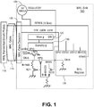
- FIG. 1 is an illustration of an embodiment of a system including low power standby mode control.
- a sink device such as an MHL sink 100 is coupled via a cable, illustrated as MHL cable 115, with a source device (such as a smart phone) containing an MHL transmitter 110.
- the MHL sink 110 includes a cable detection element 120 to detect connection of a source device.
- Connections include RPWR (a voltage bus, or V-bus) and a control bus (CBUS), where RPWR is coupled with a voltage regulator 105 to provide a 5V, 500 mA regulated voltage source in this example.
- RPWR a voltage bus, or V-bus
- CBUS control bus
- the regulated voltage is provided to a main microprocessor 125, while a standby mode microprocessor 130, coupled to the main microprocessor, receives a standby voltage, whereby the standby microprocessor may be a part of a standby mode control circuit.
- the MHL sink 100 includes an MHL receiver 135, which is coupled with RPWR and is coupled with a connection to CBUS via FET2, where a signal via FET5 alternatively switches FET2 on (providing CBUS to the MHL receiver 135) or switches FET1 on to provide a pulldown path to ground through resistor R.
- the CBUS provides a signal to switch FET4, to provide a path to ground for the standby voltage.
- power pins other than the low power standby pin do not receive power in a standby mode. While an apparatus is in standby mode, the power connections are disabled such that regular power supply does not consume power, while the low power supply power pin is active to allow for triggering normal operation when a stimulus is received from outside of the chip. Thus, in the standby mode, only the low power supply power pin for a chip is consuming power, where the resulting current consumption may be significantly much lower than the static leakage current of MICOMVDD33.
- an operation includes:
- Figures 2 and 3 illustrate the operation of low power standby mode.
- Figure 2 is an illustration of elements of an embodiment of an apparatus or system providing low power standby mode control.
- an apparatus or system includes a plurality of driver elements 205, illustrated as a number n of CBUS_HPD Drivers, receiving voltage Vcc, each driver being coupled with a standby control 210 receiving voltage LPSBV.
- each standby control element 210 is coupled with LPSB_POC 215 (powered by the LPSBV), each standby control including a connection to a pad for a stimulus signal, CBUS_HPD (shown as CBUS_HPD0 through CBUS_HPDn), and each being connected to a low power control (LPCRTL) line.
- CBUS_HPD shown as CBUS_HPD0 through CBUS_HPDn
- LPCRTL low power control
- FIG. 3 illustrates an embodiment of a standby control block of an apparatus or system.
- the standby control block 300 includes a sub-block 305 to receive an LP_POC signal and generate an lpsb (low power standby) signal via two inverter elements.
- a standby control block 300 receives iCBUS_HPD and produces the stimulus signal CBUS_HPD, wherein a circuit branch 310 is coupled with a resistance, a first transistor (FET) receiving FPSBV at a gate, and a second FET receiving lpsb at a gate.
- the standby control block 300 provides LPCTRL (low power control).
- a process includes:
- network or “communication network” mean an interconnection network to deliver digital media content (including music, audio/video, gaming, photos, and others) between devices.
- a network may include a personal entertainment network, such as a network in a household, a network in a business setting, or any other network of devices and/or components.
- certain network devices may be a source of media content, such as a digital television tuner, cable set-top box, video storage server, and other source device.
- Other devices may display or use media content, such as a digital television, home theater system, audio system, gaming system, or presented over the Internet in a browser, and other devices.
- certain devices may be intended to store or transfer media content, such as video and audio storage servers.
- Certain devices may perform multiple media functions.
- the network devices may be co-located in a single local area network.
- the network devices may span multiple network segments, such as through tunneling between local area networks.
- the network may include multiple data encoding and encryption processes.
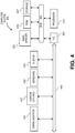
- Figure 4 illustrates a device or computer system 400 on which embodiments of the present invention may be implemented.
- the device or computer system 400 includes a low power standby mode control circuit, such as illustrated in Figures 1-3 , the standby control circuit to provide for reduced power consumption in standby mode.
- Device or computer system 400 includes a system bus 420 for communicating information, and a processor 410 coupled to bus 420 for processing information.
- processor 410 is implemented using one of the multitudes of microprocessors. Nevertheless, one of ordinary skill in the art will appreciate that other processors may be used.
- Computer system 400 further comprises a random access memory (RAM) or other dynamic storage device 425 (referred to herein as main memory), coupled to bus 420 for storing information and instructions to be executed by processor 410.
- Main memory 425 also may be used for storing temporary variables or other intermediate information during execution of instructions by processor 410.
- Computer system 400 also may include a read only memory (ROM) and or other static storage device 426 coupled to bus 420 for storing static information and instructions used by processor 410.
- ROM read only memory
- a data storage device 427 such as a magnetic disk or optical disc and its corresponding drive may also be coupled to computer system 400 for storing information and instructions.
- Computer system 400 can also be coupled to a second input/output (I/O) bus 450 via an I/O interface 430.
- I/O input/output
- a plurality of I/O devices may be coupled to I/O bus 450, including a display device 424, an input device (e.g., an alphanumeric input device 423 and or a cursor control device 422).
- the communication device 421 is for accessing other computers (servers or clients) via external data network.
- the communication device 421 may comprise a modem, a network interface card, or other well-known interface device, such as those used for coupling to Ethernet, token ring, or other types of networks.
- Computer system 400 includes, but is not limited to, a network computer device, a mobile telephone, a personal data assistant (PDA), etc.
- PDA personal data assistant
- Computer system 400 may be interconnected in a client/server network system.
- a network may include a Local Area Network (LAN), Wide Area Network (WAN), Metropolitan Area Network (MAN), intranet, the Internet, etc. Any number of network devices can be cascaded into being connected with a port multiplier forming a networking mechanism within a network. It is contemplated that there may be any number of devices connected via the network.
- a device may transfer data streams, such as streaming media data, to other devices in the network system via a number of standard and non-standard protocols, including the protocols described in this document.
- Various embodiments of the present invention may include various processes. These processes may be performed by hardware components or may be embodied in computer program or machine-executable instructions, which may be used to cause a general-purpose or special-purpose processor or logic circuits programmed with the instructions to perform the processes. Alternatively, the processes may be performed by a combination of hardware and software.
- modules, components, or elements described throughout this document may include hardware, software, and/or a combination thereof.
- a module includes software
- the software data, instructions, and/or configuration may be provided via an article of manufacture by a machine/electronic device/hardware.
- An article of manufacture may include a non-transitory computer-readable storage medium having content to provide instructions, data, etc.
- Portions of various embodiments of the present invention may be provided as a computer program product, which may include a non-transitory computer-readable storage medium having stored thereon computer program instructions, which may be used to program a computer (or other electronic devices) to perform a process according to the embodiments of the present invention.
- the computer-readable medium may include, but is not limited to, floppy diskettes, optical disks, compact disk read-only memory (CD-ROM), and magneto-optical disks, read-only memory (ROM), random access memory (RAM), erasable programmable read-only memory (EPROM), EEPROM, magnet or optical cards, flash memory, or other type of media/machine-readable medium suitable for storing electronic instructions.
- the present invention according to claim 13 may also be downloaded as a computer program product, wherein the program may be transferred from a remote computer to a requesting computer.
Landscapes
- Engineering & Computer Science (AREA)
- Theoretical Computer Science (AREA)
- General Engineering & Computer Science (AREA)
- Physics & Mathematics (AREA)
- General Physics & Mathematics (AREA)
- Computer Hardware Design (AREA)
- Computing Systems (AREA)
- Power Sources (AREA)
- Microcomputers (AREA)
- Telephone Function (AREA)
Claims (13)
- Eine Vorrichtung (100) zur Steuerung eines leistungsarmen Standby-Modus, aufweisend:einen Prozessor (125) zum Aktivieren oder Deaktivieren von einer oder mehreren Stromverbindungen zu einer Betriebsschaltung (135), um dadurch zu bewirken, dass die Betriebsschaltung in verschiedenen Modi betrieben wird;eine Schnittstelle für eine Kabel (115) -Verbindung mit einer zweiten Vorrichtung (110);ein Erfassungselement (120) zum Erfassen der Kabelverbindung mit der zweiten Vorrichtung an der Schnittstelle;wobei die Betriebsschaltung in einem Standby-Modus oder einem Aktiv-Modus betrieben wird, wobei die Betriebsschaltung in dem Standby-Modus betrieben wird als Antwort auf ein Deaktivieren der einen oder mehreren Stromverbindungen durch den Prozessor, oder in dem Aktiv-Modus betrieben wird als Antwort auf ein Aktivieren der einen oder mehreren Stromverbindungen durch den Prozessor; undeine Standby-Modus-Steuerschaltung (130), welche mit dem Prozessor (125) verbunden ist und unter Verwendung einer Standby-Stromquelle betrieben wird, wobei die Standby-Modus-Steuerschaltung ein Stimulussignal von der zweiten Vorrichtung erfasst und, als Antwort auf das Stimulussignal, die Standby-Modus-Steuerschaltung dem Prozessor signalisiert, die eine oder mehreren Stromverbindungen der Betriebsschaltung zu aktivieren,wobei das Stimulussignal von der zweiten Vorrichtung über einen Steuerbus (CBUS) empfangen wird, der mit dem Erfassungselement verbunden ist, welches die Kabelverbindung mit der zweiten Vorrichtung erfasst, wobei der Steuerbus mit der Betriebsschaltung verbunden ist.
- Die Vorrichtung gemäß Anspruch 1, wobei die Betriebsschaltung ein Empfänger-Chip ist.
- Die Vorrichtung gemäß Anspruch 1, wobei die Vorrichtung eine Mobile-High-Definition-Link (MHL)-kompatible Vorrichtung ist.
- Die Vorrichtung gemäß Anspruch 1, wobei die Betriebsschaltung eine Mehrzahl von Transistorelementen aufweist, wobei die Transistorelemente deaktiviert werden, wenn die eine oder die mehreren Stromverbindungen deaktiviert werden.
- Die Vorrichtung gemäß Anspruch 1, wobei die Betriebsschaltung in dem Standby-Modus in einen Ausgeschaltet-Zustand gebracht wird.
- Die Vorrichtung gemäß Anspruch 1, ferner aufweisend einen ersten Schalter (FET2), um den Steuerbus mit der Betriebsschaltung zu verbinden und als Antwort darauf, dass das Erfassungselement die Kabelverbindung mit der zweiten Vorrichtung erfasst, angeschaltet zu werden.
- Die Vorrichtung gemäß Anspruch 1, wobei das Stimulussignal eine Spannungspegeländerung auf dem Steuerbus ist.
- Ein Verfahren zum Steuern eines leistungsarmen Standby-Modus, aufweisend:Überführen einer Vorrichtung (100) oder eines Systems in einen Standby-Modus;Deaktivieren, durch einen Prozessor (125), von einer oder mehreren Stromverbindungen zu einem Betriebsschaltkreis (135);Betreiben einer Standby-Modus-Steuerschaltung an einer Standby-Stromquelle;Erfassen, durch ein Erfassungselement (120), einer Kabel (115) -Verbindung mit einer zweiten Vorrichtung oder einem zweiten System;Empfangen eines Stimulussignals von der zweiten Vorrichtung oder dem zweiten System an der Standby-Modus-Steuerschaltung; undErzeugen, als Antwort auf das Stimulussignal, eines Signals von der Standby-Modus-Steuerschaltung an den Prozessor, wobei der Prozessor als Antwort auf das Signal von der Standby-Modus-Steuerschaltung eine oder mehrere Stromverbindungen aktiviert,wobei das Stimulus signal von der zweiten Vorrichtung oder dem zweiten System über einen Steuerbus (CBUS) empfangen wird, welcher mit dem Erfassungselement, das die Kabelverbindung mit der zweiten Vorrichtung oder dem zweiten System erfasst, verbunden ist, wobei der Steuerbus mit der Betriebsschaltung verbunden ist.
- Das Verfahren gemäß Anspruch 8, wobei ein Deaktivieren von einer oder mehreren Stromverbindungen die Betriebsschaltung in einen Strom-Aus-Modus versetzt.
- Das Verfahren gemäß Anspruch 8, ferner aufweisend ein Reduzieren eines Ableitstromverbrauchs der Vorrichtung oder des Systems durch Deaktivieren einer Mehrzahl von Transistoren der Betriebsschaltung in dem Standby-Modus.
- Das Verfahren gemäß Anspruch 8, wobei die Betriebsschaltung ein Empfänger-Chip ist.
- Das Verfahren gemäß Anspruch 8, wobei die Vorrichtung oder das System eine Mobile-High-Definition-Link (MHL)-kompatible Vorrichtung oder ein Mobile-High-Definition-Link (MHL)-kompatibles System ist.
- Ein maschinenlesbares Medium, welches eine Mehrzahl von Instruktionen aufweist, die als Antwort auf deren Ausführung auf einer Rechenvorrichtung bewirken, dass die Rechenvorrichtung Operationen gemäß irgendeinem der Ansprüche 8 bis 12 ausführt.
Applications Claiming Priority (3)
| Application Number | Priority Date | Filing Date | Title |
|---|---|---|---|
| US201161440131P | 2011-02-07 | 2011-02-07 | |
| US13/362,930 US9015509B2 (en) | 2011-02-07 | 2012-01-31 | Mechanism for low power standby mode control circuit |
| PCT/US2012/023940 WO2012109128A2 (en) | 2011-02-07 | 2012-02-06 | Mechanism for low power standby mode control circuit |
Publications (3)
| Publication Number | Publication Date |
|---|---|
| EP2673685A2 EP2673685A2 (de) | 2013-12-18 |
| EP2673685A4 EP2673685A4 (de) | 2015-08-05 |
| EP2673685B1 true EP2673685B1 (de) | 2018-08-01 |
Family
ID=46601500
Family Applications (1)
| Application Number | Title | Priority Date | Filing Date |
|---|---|---|---|
| EP12744257.2A Active EP2673685B1 (de) | 2011-02-07 | 2012-02-06 | Mechanismus für eine steuerschaltung mit einem standby-modus mit geringem stromverbrauch |
Country Status (7)
| Country | Link |
|---|---|
| US (1) | US9015509B2 (de) |
| EP (1) | EP2673685B1 (de) |
| JP (1) | JP5746771B2 (de) |
| KR (1) | KR101912599B1 (de) |
| CN (1) | CN103348304B (de) |
| TW (1) | TWI541639B (de) |
| WO (1) | WO2012109128A2 (de) |
Families Citing this family (13)
| Publication number | Priority date | Publication date | Assignee | Title |
|---|---|---|---|---|
| JP5446439B2 (ja) * | 2008-07-24 | 2014-03-19 | 富士通株式会社 | 通信制御装置、データ保全システム、通信制御方法、およびプログラム |
| US10231017B2 (en) | 2012-10-16 | 2019-03-12 | Sony Corporation | Electronic device, charging control method of electronic device, battery power-level display method of electronic device, source device, and sink device |
| US9197340B2 (en) | 2012-10-16 | 2015-11-24 | Cadence Design Systems Inc. | Connector and interface circuit for simultaneous content streaming and user data from handheld devices |
| US9026820B2 (en) * | 2012-12-29 | 2015-05-05 | Intel Corporation | Communication link and network connectivity management in low power mode |
| WO2014207910A1 (ja) * | 2013-06-28 | 2014-12-31 | 株式会社 東芝 | テレビジョン装置、及びリモートコントローラ |
| CN103533281B (zh) * | 2013-09-27 | 2017-01-11 | 广州视源电子科技股份有限公司 | 增强兼容性的mhl识别控制电路 |
| US20160282922A1 (en) * | 2013-11-20 | 2016-09-29 | Entropic Communications, Llc | Network Sensing Systems and Methods for Power Management |
| WO2015099802A1 (en) | 2013-12-28 | 2015-07-02 | Intel Corporation | Techniques for increasing energy efficiency of sensor controllers |
| US9449655B1 (en) | 2015-08-31 | 2016-09-20 | Cypress Semiconductor Corporation | Low standby power with fast turn on for non-volatile memory devices |
| CN113553000B (zh) * | 2018-07-18 | 2024-04-12 | 成都忆芯科技有限公司 | 降低集成电路功耗的方法及其控制电路 |
| KR20200144738A (ko) | 2019-06-19 | 2020-12-30 | 휴렛-팩커드 디벨롭먼트 컴퍼니, 엘.피. | 케이블 연결에 상태에 기초한 소비 전력 저감 |
| KR102505073B1 (ko) * | 2020-08-25 | 2023-02-28 | 동명대학교산학협력단 | 인공 지능형 절전 콘센트 시스템 |
| KR102505741B1 (ko) * | 2020-08-25 | 2023-03-02 | 동명대학교산학협력단 | 인공 지능형 절전 콘센트 |
Family Cites Families (18)
| Publication number | Priority date | Publication date | Assignee | Title |
|---|---|---|---|---|
| KR100234423B1 (ko) * | 1995-12-05 | 1999-12-15 | 윤종용 | 컴퓨터 주변기기의 전원제어 장치 및 방법 |
| US6308278B1 (en) | 1997-12-29 | 2001-10-23 | Intel Corporation | Supplying standby voltage to memory and wakeup circuitry to wake a computer from a low power mode |
| US6131167A (en) * | 1997-12-31 | 2000-10-10 | Intel Corporation | Method and apparatus to reduce power consumption on a bus |
| US7266389B2 (en) * | 2002-08-12 | 2007-09-04 | Broadcom Corporation | Device for selective power management for a hand held host |
| JP4625712B2 (ja) * | 2005-04-14 | 2011-02-02 | パナソニック株式会社 | 半導体集積回路及び電子機器 |
| EP1785809A1 (de) * | 2005-11-14 | 2007-05-16 | Texas Instruments Inc. | Bereitschaftsmodus für Stromverwaltung |
| JP2008067024A (ja) * | 2006-09-07 | 2008-03-21 | Sharp Corp | 表示装置及び表示システム |
| US20100014002A1 (en) * | 2007-01-10 | 2010-01-21 | Shenzhen Tcl New Technology Ltd | System and method for control line isolation |
| JP2008204267A (ja) * | 2007-02-21 | 2008-09-04 | Matsushita Electric Ind Co Ltd | 送信デバイス |
| US8086886B2 (en) | 2007-08-31 | 2011-12-27 | Silicon Image, Inc. | Group power management of network devices |
| KR20090065905A (ko) * | 2007-12-18 | 2009-06-23 | 삼성전자주식회사 | 영상처리장치, 영상처리시스템 및 영상처리장치의전원제어방법 |
| EP2283650A1 (de) * | 2008-05-26 | 2011-02-16 | Koninklijke Philips Electronics N.V. | Verfahren zur umschaltung einer multimedia-quelle und einer multimedia-senke von einem betriebsmodus in einen standby-modus und von einem standby-modus in einen betriebsmodus |
| US8275914B2 (en) * | 2008-10-16 | 2012-09-25 | Silicon Image, Inc. | Discovery of connections utilizing a control bus |
| JP2010140291A (ja) * | 2008-12-12 | 2010-06-24 | Sony Corp | データ受信装置および電源制御方法 |
| KR101512493B1 (ko) | 2009-02-06 | 2015-04-15 | 삼성전자주식회사 | 저전력 시스템온칩 |
| CN201556159U (zh) * | 2009-06-30 | 2010-08-18 | 青岛海信电器股份有限公司 | 一种低功耗待机电路以及具有所述电路的液晶显示装置 |
| KR101158715B1 (ko) * | 2009-07-24 | 2012-06-22 | 삼성전자주식회사 | 화상형성장치 및 그의 저전력 제어방법 |
| EP2391056B1 (de) * | 2010-05-26 | 2013-08-21 | Samsung Electronics Co., Ltd. | Medienspieler und Verfahren zur Rückholung aus dem Ruhemodus |
-
2012
- 2012-01-31 US US13/362,930 patent/US9015509B2/en active Active
- 2012-02-06 WO PCT/US2012/023940 patent/WO2012109128A2/en not_active Ceased
- 2012-02-06 KR KR1020137023526A patent/KR101912599B1/ko active Active
- 2012-02-06 CN CN201280007877.2A patent/CN103348304B/zh active Active
- 2012-02-06 EP EP12744257.2A patent/EP2673685B1/de active Active
- 2012-02-06 JP JP2013552707A patent/JP5746771B2/ja active Active
- 2012-02-07 TW TW101104002A patent/TWI541639B/zh active
Non-Patent Citations (1)
| Title |
|---|
| None * |
Also Published As
| Publication number | Publication date |
|---|---|
| US20120204048A1 (en) | 2012-08-09 |
| KR20140045337A (ko) | 2014-04-16 |
| JP5746771B2 (ja) | 2015-07-08 |
| EP2673685A4 (de) | 2015-08-05 |
| TW201245949A (en) | 2012-11-16 |
| CN103348304B (zh) | 2016-12-21 |
| KR101912599B1 (ko) | 2018-10-29 |
| JP2014510964A (ja) | 2014-05-01 |
| CN103348304A (zh) | 2013-10-09 |
| US9015509B2 (en) | 2015-04-21 |
| TWI541639B (zh) | 2016-07-11 |
| EP2673685A2 (de) | 2013-12-18 |
| WO2012109128A2 (en) | 2012-08-16 |
| WO2012109128A3 (en) | 2013-01-10 |
Similar Documents
| Publication | Publication Date | Title |
|---|---|---|
| EP2673685B1 (de) | Mechanismus für eine steuerschaltung mit einem standby-modus mit geringem stromverbrauch | |
| US7895458B2 (en) | Power control apparatus and method thereof | |
| US9471140B2 (en) | Valid context status retention in processor power mode management | |
| CN104272388A (zh) | 存储器装置的超深断电模式 | |
| US8429432B2 (en) | Stand-by power system for information handling systems | |
| KR102151178B1 (ko) | 직렬 통신 장치 및 그 방법 | |
| CN103959648A (zh) | 节约电荷的功率门控装置和方法 | |
| TW201525662A (zh) | 用於電子系統之接續供電之競爭防止 | |
| US7093140B2 (en) | Method and apparatus for configuring a voltage regulator based on current information | |
| US6857079B2 (en) | Integrated driver electronic (IDE) device power control | |
| KR20230004864A (ko) | 직렬 데이터 통신 인터페이스를 통해 시스템 및 전력 관리를 수행하기 위한 방법 | |
| KR20010060239A (ko) | 입출력 포트의 보전성을 유지하면서 전원이 차단되는 코어로직을 갖는 마이크로 컨트롤러 | |
| US6853221B1 (en) | Power-up detection circuit with low current draw for dual power supply circuits | |
| US20130339761A1 (en) | Power management system for electronic circuit | |
| US6784647B2 (en) | Method and apparatus for operating a voltage regulator based on operation of a timer | |
| US20110080266A1 (en) | Power Controller for an Electronic Reader Device | |
| CN106301804A (zh) | 一种实现网络唤醒的服务器、系统及方法 | |
| US9996143B2 (en) | Apparatus and method for selectively disabling one or more analog circuits of a processor during a low power state of the processor | |
| US7321980B2 (en) | Software power control of circuit modules in a shared and distributed DMA system | |
| US20060031693A1 (en) | Computer peripheral | |
| CN101335512A (zh) | 具有待机功能的电子装置 | |
| WO2025241144A1 (zh) | 一种终端设备的启动方法、终端设备及存储介质 | |
| TW202536598A (zh) | 用以減少延遲及功耗之半導體系統 | |
| CN102692989A (zh) | 操作系统及其控制方法 | |
| CN106227292A (zh) | 时钟控制设备、方法和触控显示设备 |
Legal Events
| Date | Code | Title | Description |
|---|---|---|---|
| PUAI | Public reference made under article 153(3) epc to a published international application that has entered the european phase |
Free format text: ORIGINAL CODE: 0009012 |
|
| 17P | Request for examination filed |
Effective date: 20130822 |
|
| AK | Designated contracting states |
Kind code of ref document: A2 Designated state(s): AL AT BE BG CH CY CZ DE DK EE ES FI FR GB GR HR HU IE IS IT LI LT LU LV MC MK MT NL NO PL PT RO RS SE SI SK SM TR |
|
| DAX | Request for extension of the european patent (deleted) | ||
| A4 | Supplementary search report drawn up and despatched |
Effective date: 20150703 |
|
| RIC1 | Information provided on ipc code assigned before grant |
Ipc: G06F 1/32 20060101AFI20150629BHEP |
|
| GRAP | Despatch of communication of intention to grant a patent |
Free format text: ORIGINAL CODE: EPIDOSNIGR1 |
|
| STAA | Information on the status of an ep patent application or granted ep patent |
Free format text: STATUS: GRANT OF PATENT IS INTENDED |
|
| INTG | Intention to grant announced |
Effective date: 20180124 |
|
| RAP1 | Party data changed (applicant data changed or rights of an application transferred) |
Owner name: LATTICE SEMICONDUCTOR CORPORATION |
|
| GRAJ | Information related to disapproval of communication of intention to grant by the applicant or resumption of examination proceedings by the epo deleted |
Free format text: ORIGINAL CODE: EPIDOSDIGR1 |
|
| STAA | Information on the status of an ep patent application or granted ep patent |
Free format text: STATUS: REQUEST FOR EXAMINATION WAS MADE |
|
| GRAR | Information related to intention to grant a patent recorded |
Free format text: ORIGINAL CODE: EPIDOSNIGR71 |
|
| GRAS | Grant fee paid |
Free format text: ORIGINAL CODE: EPIDOSNIGR3 |
|
| STAA | Information on the status of an ep patent application or granted ep patent |
Free format text: STATUS: GRANT OF PATENT IS INTENDED |
|
| INTC | Intention to grant announced (deleted) | ||
| GRAA | (expected) grant |
Free format text: ORIGINAL CODE: 0009210 |
|
| STAA | Information on the status of an ep patent application or granted ep patent |
Free format text: STATUS: THE PATENT HAS BEEN GRANTED |
|
| AK | Designated contracting states |
Kind code of ref document: B1 Designated state(s): AL AT BE BG CH CY CZ DE DK EE ES FI FR GB GR HR HU IE IS IT LI LT LU LV MC MK MT NL NO PL PT RO RS SE SI SK SM TR |
|
| INTG | Intention to grant announced |
Effective date: 20180625 |
|
| REG | Reference to a national code |
Ref country code: GB Ref legal event code: FG4D |
|
| REG | Reference to a national code |
Ref country code: CH Ref legal event code: EP Ref country code: AT Ref legal event code: REF Ref document number: 1025039 Country of ref document: AT Kind code of ref document: T Effective date: 20180815 |
|
| REG | Reference to a national code |
Ref country code: IE Ref legal event code: FG4D |
|
| REG | Reference to a national code |
Ref country code: DE Ref legal event code: R096 Ref document number: 602012049138 Country of ref document: DE |
|
| REG | Reference to a national code |
Ref country code: NL Ref legal event code: MP Effective date: 20180801 |
|
| REG | Reference to a national code |
Ref country code: LT Ref legal event code: MG4D |
|
| REG | Reference to a national code |
Ref country code: AT Ref legal event code: MK05 Ref document number: 1025039 Country of ref document: AT Kind code of ref document: T Effective date: 20180801 |
|
| PG25 | Lapsed in a contracting state [announced via postgrant information from national office to epo] |
Ref country code: SE Free format text: LAPSE BECAUSE OF FAILURE TO SUBMIT A TRANSLATION OF THE DESCRIPTION OR TO PAY THE FEE WITHIN THE PRESCRIBED TIME-LIMIT Effective date: 20180801 Ref country code: BG Free format text: LAPSE BECAUSE OF FAILURE TO SUBMIT A TRANSLATION OF THE DESCRIPTION OR TO PAY THE FEE WITHIN THE PRESCRIBED TIME-LIMIT Effective date: 20181101 Ref country code: NL Free format text: LAPSE BECAUSE OF FAILURE TO SUBMIT A TRANSLATION OF THE DESCRIPTION OR TO PAY THE FEE WITHIN THE PRESCRIBED TIME-LIMIT Effective date: 20180801 Ref country code: AT Free format text: LAPSE BECAUSE OF FAILURE TO SUBMIT A TRANSLATION OF THE DESCRIPTION OR TO PAY THE FEE WITHIN THE PRESCRIBED TIME-LIMIT Effective date: 20180801 Ref country code: IS Free format text: LAPSE BECAUSE OF FAILURE TO SUBMIT A TRANSLATION OF THE DESCRIPTION OR TO PAY THE FEE WITHIN THE PRESCRIBED TIME-LIMIT Effective date: 20181201 Ref country code: GR Free format text: LAPSE BECAUSE OF FAILURE TO SUBMIT A TRANSLATION OF THE DESCRIPTION OR TO PAY THE FEE WITHIN THE PRESCRIBED TIME-LIMIT Effective date: 20181102 Ref country code: RS Free format text: LAPSE BECAUSE OF FAILURE TO SUBMIT A TRANSLATION OF THE DESCRIPTION OR TO PAY THE FEE WITHIN THE PRESCRIBED TIME-LIMIT Effective date: 20180801 Ref country code: NO Free format text: LAPSE BECAUSE OF FAILURE TO SUBMIT A TRANSLATION OF THE DESCRIPTION OR TO PAY THE FEE WITHIN THE PRESCRIBED TIME-LIMIT Effective date: 20181101 Ref country code: FI Free format text: LAPSE BECAUSE OF FAILURE TO SUBMIT A TRANSLATION OF THE DESCRIPTION OR TO PAY THE FEE WITHIN THE PRESCRIBED TIME-LIMIT Effective date: 20180801 Ref country code: LT Free format text: LAPSE BECAUSE OF FAILURE TO SUBMIT A TRANSLATION OF THE DESCRIPTION OR TO PAY THE FEE WITHIN THE PRESCRIBED TIME-LIMIT Effective date: 20180801 Ref country code: PL Free format text: LAPSE BECAUSE OF FAILURE TO SUBMIT A TRANSLATION OF THE DESCRIPTION OR TO PAY THE FEE WITHIN THE PRESCRIBED TIME-LIMIT Effective date: 20180801 |
|
| PG25 | Lapsed in a contracting state [announced via postgrant information from national office to epo] |
Ref country code: LV Free format text: LAPSE BECAUSE OF FAILURE TO SUBMIT A TRANSLATION OF THE DESCRIPTION OR TO PAY THE FEE WITHIN THE PRESCRIBED TIME-LIMIT Effective date: 20180801 Ref country code: HR Free format text: LAPSE BECAUSE OF FAILURE TO SUBMIT A TRANSLATION OF THE DESCRIPTION OR TO PAY THE FEE WITHIN THE PRESCRIBED TIME-LIMIT Effective date: 20180801 Ref country code: AL Free format text: LAPSE BECAUSE OF FAILURE TO SUBMIT A TRANSLATION OF THE DESCRIPTION OR TO PAY THE FEE WITHIN THE PRESCRIBED TIME-LIMIT Effective date: 20180801 |
|
| PG25 | Lapsed in a contracting state [announced via postgrant information from national office to epo] |
Ref country code: RO Free format text: LAPSE BECAUSE OF FAILURE TO SUBMIT A TRANSLATION OF THE DESCRIPTION OR TO PAY THE FEE WITHIN THE PRESCRIBED TIME-LIMIT Effective date: 20180801 Ref country code: CZ Free format text: LAPSE BECAUSE OF FAILURE TO SUBMIT A TRANSLATION OF THE DESCRIPTION OR TO PAY THE FEE WITHIN THE PRESCRIBED TIME-LIMIT Effective date: 20180801 Ref country code: ES Free format text: LAPSE BECAUSE OF FAILURE TO SUBMIT A TRANSLATION OF THE DESCRIPTION OR TO PAY THE FEE WITHIN THE PRESCRIBED TIME-LIMIT Effective date: 20180801 Ref country code: IT Free format text: LAPSE BECAUSE OF FAILURE TO SUBMIT A TRANSLATION OF THE DESCRIPTION OR TO PAY THE FEE WITHIN THE PRESCRIBED TIME-LIMIT Effective date: 20180801 Ref country code: EE Free format text: LAPSE BECAUSE OF FAILURE TO SUBMIT A TRANSLATION OF THE DESCRIPTION OR TO PAY THE FEE WITHIN THE PRESCRIBED TIME-LIMIT Effective date: 20180801 |
|
| REG | Reference to a national code |
Ref country code: DE Ref legal event code: R097 Ref document number: 602012049138 Country of ref document: DE |
|
| PG25 | Lapsed in a contracting state [announced via postgrant information from national office to epo] |
Ref country code: SK Free format text: LAPSE BECAUSE OF FAILURE TO SUBMIT A TRANSLATION OF THE DESCRIPTION OR TO PAY THE FEE WITHIN THE PRESCRIBED TIME-LIMIT Effective date: 20180801 Ref country code: SM Free format text: LAPSE BECAUSE OF FAILURE TO SUBMIT A TRANSLATION OF THE DESCRIPTION OR TO PAY THE FEE WITHIN THE PRESCRIBED TIME-LIMIT Effective date: 20180801 Ref country code: DK Free format text: LAPSE BECAUSE OF FAILURE TO SUBMIT A TRANSLATION OF THE DESCRIPTION OR TO PAY THE FEE WITHIN THE PRESCRIBED TIME-LIMIT Effective date: 20180801 |
|
| PLBE | No opposition filed within time limit |
Free format text: ORIGINAL CODE: 0009261 |
|
| STAA | Information on the status of an ep patent application or granted ep patent |
Free format text: STATUS: NO OPPOSITION FILED WITHIN TIME LIMIT |
|
| 26N | No opposition filed |
Effective date: 20190503 |
|
| PG25 | Lapsed in a contracting state [announced via postgrant information from national office to epo] |
Ref country code: SI Free format text: LAPSE BECAUSE OF FAILURE TO SUBMIT A TRANSLATION OF THE DESCRIPTION OR TO PAY THE FEE WITHIN THE PRESCRIBED TIME-LIMIT Effective date: 20180801 |
|
| REG | Reference to a national code |
Ref country code: CH Ref legal event code: PL |
|
| PG25 | Lapsed in a contracting state [announced via postgrant information from national office to epo] |
Ref country code: MC Free format text: LAPSE BECAUSE OF FAILURE TO SUBMIT A TRANSLATION OF THE DESCRIPTION OR TO PAY THE FEE WITHIN THE PRESCRIBED TIME-LIMIT Effective date: 20180801 Ref country code: LU Free format text: LAPSE BECAUSE OF NON-PAYMENT OF DUE FEES Effective date: 20190206 |
|
| REG | Reference to a national code |
Ref country code: BE Ref legal event code: MM Effective date: 20190228 |
|
| REG | Reference to a national code |
Ref country code: IE Ref legal event code: MM4A |
|
| PG25 | Lapsed in a contracting state [announced via postgrant information from national office to epo] |
Ref country code: CH Free format text: LAPSE BECAUSE OF NON-PAYMENT OF DUE FEES Effective date: 20190228 Ref country code: LI Free format text: LAPSE BECAUSE OF NON-PAYMENT OF DUE FEES Effective date: 20190228 |
|
| PG25 | Lapsed in a contracting state [announced via postgrant information from national office to epo] |
Ref country code: IE Free format text: LAPSE BECAUSE OF NON-PAYMENT OF DUE FEES Effective date: 20190206 |
|
| PG25 | Lapsed in a contracting state [announced via postgrant information from national office to epo] |
Ref country code: BE Free format text: LAPSE BECAUSE OF NON-PAYMENT OF DUE FEES Effective date: 20190228 |
|
| PG25 | Lapsed in a contracting state [announced via postgrant information from national office to epo] |
Ref country code: TR Free format text: LAPSE BECAUSE OF FAILURE TO SUBMIT A TRANSLATION OF THE DESCRIPTION OR TO PAY THE FEE WITHIN THE PRESCRIBED TIME-LIMIT Effective date: 20180801 |
|
| PG25 | Lapsed in a contracting state [announced via postgrant information from national office to epo] |
Ref country code: PT Free format text: LAPSE BECAUSE OF FAILURE TO SUBMIT A TRANSLATION OF THE DESCRIPTION OR TO PAY THE FEE WITHIN THE PRESCRIBED TIME-LIMIT Effective date: 20181201 Ref country code: MT Free format text: LAPSE BECAUSE OF NON-PAYMENT OF DUE FEES Effective date: 20190206 |
|
| PG25 | Lapsed in a contracting state [announced via postgrant information from national office to epo] |
Ref country code: CY Free format text: LAPSE BECAUSE OF FAILURE TO SUBMIT A TRANSLATION OF THE DESCRIPTION OR TO PAY THE FEE WITHIN THE PRESCRIBED TIME-LIMIT Effective date: 20180801 |
|
| PG25 | Lapsed in a contracting state [announced via postgrant information from national office to epo] |
Ref country code: HU Free format text: LAPSE BECAUSE OF FAILURE TO SUBMIT A TRANSLATION OF THE DESCRIPTION OR TO PAY THE FEE WITHIN THE PRESCRIBED TIME-LIMIT; INVALID AB INITIO Effective date: 20120206 |
|
| PG25 | Lapsed in a contracting state [announced via postgrant information from national office to epo] |
Ref country code: MK Free format text: LAPSE BECAUSE OF FAILURE TO SUBMIT A TRANSLATION OF THE DESCRIPTION OR TO PAY THE FEE WITHIN THE PRESCRIBED TIME-LIMIT Effective date: 20180801 |
|
| P01 | Opt-out of the competence of the unified patent court (upc) registered |
Effective date: 20230929 |
|
| PGFP | Annual fee paid to national office [announced via postgrant information from national office to epo] |
Ref country code: DE Payment date: 20250227 Year of fee payment: 14 |
|
| PGFP | Annual fee paid to national office [announced via postgrant information from national office to epo] |
Ref country code: FR Payment date: 20250225 Year of fee payment: 14 |
|
| PGFP | Annual fee paid to national office [announced via postgrant information from national office to epo] |
Ref country code: GB Payment date: 20250227 Year of fee payment: 14 |