EP2667141B1 - Heat dissipation switch - Google Patents
Heat dissipation switch Download PDFInfo
- Publication number
- EP2667141B1 EP2667141B1 EP13168615.6A EP13168615A EP2667141B1 EP 2667141 B1 EP2667141 B1 EP 2667141B1 EP 13168615 A EP13168615 A EP 13168615A EP 2667141 B1 EP2667141 B1 EP 2667141B1
- Authority
- EP
- European Patent Office
- Prior art keywords
- thermally
- heat
- conductive elements
- heat dissipation
- thermally switched
- Prior art date
- Legal status (The legal status is an assumption and is not a legal conclusion. Google has not performed a legal analysis and makes no representation as to the accuracy of the status listed.)
- Active
Links
Images


Classifications
-
- F—MECHANICAL ENGINEERING; LIGHTING; HEATING; WEAPONS; BLASTING
- F28—HEAT EXCHANGE IN GENERAL
- F28F—DETAILS OF HEAT-EXCHANGE AND HEAT-TRANSFER APPARATUS, OF GENERAL APPLICATION
- F28F13/00—Arrangements for modifying heat-transfer, e.g. increasing, decreasing
-
- H—ELECTRICITY
- H01—ELECTRIC ELEMENTS
- H01L—SEMICONDUCTOR DEVICES NOT COVERED BY CLASS H10
- H01L23/00—Details of semiconductor or other solid state devices
- H01L23/34—Arrangements for cooling, heating, ventilating or temperature compensation ; Temperature sensing arrangements
-
- F—MECHANICAL ENGINEERING; LIGHTING; HEATING; WEAPONS; BLASTING
- F28—HEAT EXCHANGE IN GENERAL
- F28F—DETAILS OF HEAT-EXCHANGE AND HEAT-TRANSFER APPARATUS, OF GENERAL APPLICATION
- F28F13/00—Arrangements for modifying heat-transfer, e.g. increasing, decreasing
- F28F2013/005—Thermal joints
- F28F2013/008—Variable conductance materials; Thermal switches
-
- H—ELECTRICITY
- H01—ELECTRIC ELEMENTS
- H01L—SEMICONDUCTOR DEVICES NOT COVERED BY CLASS H10
- H01L2924/00—Indexing scheme for arrangements or methods for connecting or disconnecting semiconductor or solid-state bodies as covered by H01L24/00
- H01L2924/0001—Technical content checked by a classifier
- H01L2924/0002—Not covered by any one of groups H01L24/00, H01L24/00 and H01L2224/00
Definitions
- Electrical components are used throughout virtually all industries. One characteristic of most electrical components is that they often produce heat during operation. While this heat is not a problem in many applications, other applications dictate that excess heat be sufficiently removed from the applicable electrical components in order to prevent damage or malfunctioning of the electrical components or of other components of an associated system.
- a heat source such as an electrical component
- a heat source may be thermally coupled to a heat sink having a higher thermal conductivity and/or lower temperature than the heat source. In doing so, heat produced by the heat source continuously flows from the heat source to the heat sink where it may be dissipated into the ambient environment. While this solution may be relatively simple and cost effective, one disadvantage is that because the heat source and heat sink are continuously coupled to one another, heat or cold may undesirably flow in a reverse direction from the ambient environment to the electrical component during times in which the component is not producing excess heat.
- Another conventional method for removing excess heat from a heat source is to use a radiator or other heat exchanger.
- heat exchangers There are numerous types of heat exchangers, most of which utilize a coolant or airflow circulated around the heat source to remove the excess heat.
- a disadvantage to these conventional systems is that they may be too bulky and expensive.
- many of these conventional systems require pumps or actuators, which presents potential reliability issues.
- a heat transfer sheet including a heat transfer layer having a first portion and a second portion provided in a position different from the first portion in a planar view of the heat transfer layer, the second portion being capable of expanding and contracting in a thickness direction of the heat transfer layer at an expansion ratio larger than that of the first portion depending on temperature changes in an object from which heat is to be dissipated.
- thermo conductivity between the object and a dissipation member is lowered due to creation of a gap between the second portion and the object and/or the dissipation member, whereas in the case where the temperature of the heat transfer layer is a predetermined temperature or higher, the thermal conductivity between the object and the dissipation member is increased due to substantial elimination of the gap.
- EP 1 394 809 A2 there is described a heat control device for a battery containing i) a radiator for dissipating heat that has generated in a battery through a charging and discharging process; and ii) a heat controller that transforms its shape by heat.
- the structure can protect a battery from anomalous overheating.
- the device protects the battery not only from over-dissipating, but also from degradation in output power characteristics of the battery.
- a heat dissipation switch as described in claim 1.
- a method of removing heat from a heat source as described in claim 14.
- Apparatus, methods, and systems described herein provide for selective heat transfer between a heat source and heat sink according to pre-determined operational temperatures.
- a heat dissipation switch may include a layer of thermally isolating material having a number of conductive element cavities.
- a number of thermally switched conductive elements may be positioned within the conductive element cavities.
- the thermally switched conductive elements may be configured to deform in response to a threshold temperature.
- the plurality of thermally switched conductive elements may be arranged in an array. In one embodiment, the plurality of thermally switched conductive elements may be not thermally coupled to one another. Each of the thermally switched conductive elements may be nested unsecured within a conductive element cavity of the thermally isolating material.
- the plurality of thermally switched conductive elements may comprise bimetallic material. Alternatively, or in addition, the plurality of thermally switched conductive elements may comprise a shape memory alloy.
- the thermally switched conductive elements may be configured to deform from a first state to a second state as a temperature increases beyond the threshold temperature and to return from the second state to the first state as the temperature decreases beyond the threshold temperature.
- the thermally switched conductive elements may be configured to deform in response to the threshold temperature comprises being configured to deform from a first state to a second state as a temperature decreases beyond the threshold temperature and to return from the second state to the first state as the temperature increases beyond the threshold temperature.
- the plurality of thermally switched conductive elements may be thermally coupled to one another to create a thermally switched sheet of conductive elements, and wherein each of the thermally switched conductive elements is nested within a conductive element cavity of the thermally isolating material.
- the plurality of thermally switched conductive elements may comprise a first subset of thermally switched conductive elements configured to deform in response to a first threshold temperature and a second subset of thermally switched conductive elements configured to deform in response to a second threshold temperature different than the first threshold temperature.
- the heat dissipation switch may be configured according to a surface mount configuration having a continuous surface area comprising thermally isolating material and the plurality of thermally switched conductive elements, the continuous surface area bounded by a perimeter of the layer of thermally isolating material.
- the heat dissipation switch may be configured according to an edge mount configuration having a surface area bordered on an outer edge by a perimeter of the layer of thermally isolating material and on an inner edge by a non-switched area.
- Each of the plurality of thermally switched conductive elements may be configured such that deformation of the thermally switched conductive element in response to the threshold temperature extends the thermally switched conductive element below a lower surface of the layer of thermally isolating material to create a heat flow path between a heat source and a heat sink positioned on opposing sides of the heat dissipation switch.
- Each of the plurality of thermally switched conductive elements may be configured such that deformation of the thermally switched conductive element in response to the threshold temperature withdraws the thermally switched conductive element from below a lower surface of the layer of thermally isolating material to interrupt a heat flow path between a heat source and a heat sink positioned on opposing sides of the heat dissipation switch.
- Each of the plurality of thermally switched conductive elements comprises a substantially flat contact surface when deformed in response to the threshold temperature.
- the heat dissipation switch further comprises according to the invention at least one supplemental layer of thermally switched conductive elements disposed in a position between a thermally switched conductive element and a heat source, wherein the at least one supplemental layer is configured to deform in response to a secondary threshold temperature different than the threshold temperature.
- the heat dissipation switch may further comprise a conductive plug of thermally conductive material disposed within a cavity of a thermally switched conductive element such that deformation of the thermally switched conductive element in response to the threshold temperature extends the thermally switched conductive element below a lower surface of the layer of thermally isolating material to create a heat flow path from a heat source, through the conductive plug, and to a heat sink positioned on opposing sides of the heat dissipation switch.
- a method of removing heat from a heat source may include providing a layer of thermally isolating material between the heat source and a heat sink.
- the thermally isolating material may have a number of conductive element cavities, in which a number of thermally switched conductive elements may be provided.
- the thermally switched conductive elements may be exposed to a threshold temperature, and in response, deform to create and/or eliminate a heat flow path from the heat source to the heat sink.
- the plurality of thermally switched conductive elements may be not thermally coupled to one another.
- Each of the thermally switched conductive elements may be nested unsecured within a conductive element cavity of the thermally isolating material.
- the plurality of thermally switched conductive elements may be thermally coupled to one another to create a thermally switched sheet of conductive elements, and wherein each of the thermally switched conductive elements is nested within a conductive element cavity of the thermally isolating material.
- the plurality of thermally switched conductive elements may comprise bimetallic material.
- the plurality of thermally switched conductive elements may comprise a shape memory alloy.
- a heat dissipation system may include a heat source, a heat sink, and a heat dissipation switch positioned between the heat source and the heat sink.
- the heat dissipation switch may include a layer of thermally isolating material having a number of conductive element cavities with a number of thermally switched conductive elements positioned within the conductive element cavities.
- the thermally switched conductive elements may be configured to deform in response to a threshold temperature to create and/or eliminate a heat flow path between the heat source and the heat sink.
- the heat dissipation switch of the system may be in accordance with the heat dissipation switch referred to above in connection with the first aspect.
- the plurality of thermally switched conductive elements may be not thermally coupled to one another.
- Each of the thermally switched conductive elements may be nested unsecured within a conductive element cavity of the thermally isolating material.
- the plurality of thermally switched conductive elements may be thermally coupled to one another to create a thermally switched sheet of conductive elements, and wherein each of the thermally switched conductive elements is nested within a conductive element cavity of the thermally isolating material.
- the plurality of thermally switched conductive elements may comprise bimetallic material.
- the plurality of thermally switched conductive elements comprises a shape memory alloy.
- a suitable application for the concepts described herein may include components that operate in space. Electrical components in space may be subjected to extremely cold temperatures when not operating, but still produce excess heat during operations. It may not be desirable to have a heat sink permanently or fixedly attached to a component since the heat sink could effectively provide a thermal path for the extremely low temperatures to the component when not in operation. Additionally, it is desirable to minimize the weight and size of all components to be used in a space environment due to the cost and payload space restrictions associated with space applications. It is further desirable to provide components and systems for space applications that require no maintenance and are as reliable as possible.
- the disclosure provided herein provides a heat dissipation switch that satisfies these aspects that are not provided by conventional solutions. It should be appreciated that while the example implementation discussed above is in the context of heat dissipation within a space environment, the disclosure provided herein may be equally applicable to any environment and application in which it is desirable to remove excess heat from a heat source.
- FIGURE 1 shows an exploded side view of a heat dissipation system 100 according to an illustrative embodiment.
- the heat dissipation system 100 includes a heat source 102, a heat sink 104, and a heat dissipation switch 106.
- the heat dissipation switch 106 is positioned between the heat source 102 and the heat sink 104.
- the heat dissipation switch is configured to thermally isolate the heat source 102 from the heat sink 104 at predetermined temperatures or temperature ranges, and to thermally couple the heat source 102 to the heat sink 104 at other predetermined temperatures or temperature ranges.
- the heat source 102 may be any electronic or other component, circuit, device, or system that produces excess heat to be removed.
- the heat sink 104 may be any thermally conductive material having a thermal conductivity and/or temperature that facilitates heat flow in a direction from the heat source 102 to the heat sink 104 when the heat sink 104 is thermally coupled to the heat source 102.
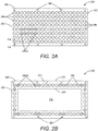
- FIGURE 2A shows a top view of a heat dissipation switch 106 configured according to a surface mount configuration 210 for coupling to a continuous area of a heat source 102 to be cooled.
- the heat dissipation switch 106 includes a thermally isolating material 202 with a number of conductive element cavities 204.
- the conductive element cavities 204 are arranged according to an array, but it should be appreciated that any desired arrangement of the conductive element cavities 204 may be used as suitable for the specific implementation of the heat dissipation switch 106.
- the conductive element cavities 204 may be apertures or compartments within the thermally isolating material 202 for nesting thermally switched conductive elements 206 within.
- the thermally isolating material 202 may include any material having a thermal conductivity that prevents or restricts heat flow from the heat source 102 and heat sink 104 positioned on opposing sides of the thermally isolating material 202. Examples of suitable material include but are not limited to polymers, ceramics, and composite materials.
- the heat dissipation switch 106 may be mounted to the heat source 102 or the heat sink 104 via mounting apertures 208, adhesive, fasteners, or any other suitable means.
- the mounting apertures 208 may align with existing mounting apertures used to traditionally mount the heat source 102 to the heat sink 104 or other component.
- the thermally switched conductive elements 206 may be any material that is capable of deformation in response to a temperature change. This deformation allows the thermally switched conductive elements 206 to extend through the conductive element cavities 204 of the thermally isolating material 202 to contact the heat source 102 on one side of the heat dissipation switch 106 and the heat sink 104 on the opposing side of the heat dissipation switch 106 in order to create a heat flow path for heat transfer from the heat source 102 to the heat sink 104. There are various materials and material combinations that may allow for this deformation. Although two embodiments will be described herein for utilization of two different types of material for the thermally switched conductive elements 206, any type of material that will provide the described deformation in response to a predetermined temperature or temperature range may be used without departing from the scope of this disclosure.
- the first type of material to be used with the thermally switched conductive elements 206 is a bimetallic material.
- Bimetallic materials include at least two materials bonded together, each having a different coefficient of thermal expansion.
- the thermally switched conductive elements 206 are generally circular or disk-shaped when viewed from the top.
- the use of bimetallic materials provides thermally switched conductive elements 206 that are capable of displacing outward from the outer surfaces of the thermally isolating material 202 when the heat source 102 raises the temperature of the thermally switched conductive elements 206 beyond the threshold temperature of the associated bimetallic material. This displacement allows the thermally switched conductive elements 206 to contact surfaces of the heat source 102 and heat sink 104, creating a heat flow path that allows for excess heat from the heat source 102 to be transferred to the heat sink 104.
- the temperature of the thermally switched conductive elements 206 lowers beyond the threshold temperature of the bimetallic material, allowing the thermally switched conductive elements 206 to return to their original shape, which breaks the contact with the heat source 102 and heat sink 104 and interrupts the heat flow path.
- the second type of material that may be used with the thermally switched conductive elements 206 is a shape memory alloy.
- Shape memory alloys are known materials that are made up of a mixture of elements. This type of alloy expands and contracts according to the temperature of the material. The expansion and contraction characteristics, as well as the corresponding activation temperature, are dependent on the particular composition of the alloy. Configuring shape memory alloys to deform in a predictable manner in response to an increase or decrease in temperature allows for the selective creation and interruption of heat transfer paths through the heat dissipation switch 106.
- the surface mount configuration 210 of the heat dissipation switch 106 of FIGURE 2A is designed to position thermally isolating material 202 and thermally switched conductive elements 206 in contact with a pre-defined surface area of the heat source 102 to provide heat transfer capabilities.
- the heat dissipation switch 106 configured in the surface mount configuration 210 has a continuous surface area of thermally isolating material 202 and thermally switched conductive elements 206 that is bounded by a perimeter 212 of the thermally isolating material 202.
- FIGURE 2B illustrates a top view of a heat dissipation switch 106 configured according to an edge mount configuration 220 for coupling to an edge or customized area of a heat source 102 to be cooled.
- the heat dissipation switch 106 has a surface area bordered on an outer edge 222 by a perimeter 212 of the thermally isolating material 202 and on an inner edge 224 by a non-switched area 226 that is central to the heat dissipation switch 106 in this example.
- the edge mount configuration 220 may be useful in applications in which it is desirable to dissipate heat from the edges or walls of a heat source 102 rather than an entire area of the heat source 102.
- the heat dissipation switch 106 may be configured according to any desired size, shape, and configuration of the interface between the heat dissipation switch 106 and the heat source 102.
- thermally switched conductive elements 206 may be positioned within any desired conductive element cavities 204 according to the desired heat dissipation positioning and performance criteria of the heat source 102.
- the custom thermally switched conductive elements 206A may be localized in particular areas in which the differing heat flow characteristics of the custom thermally switched conductive elements 206A are desirable.
- the custom thermally switched conductive elements 206A may include bimetallic material having a lower threshold temperature than the other thermally switched conductive elements 206 so that the custom thermally switched conductive elements 206A activate and deform earlier than the surrounding thermally switched conductive elements 206 as the temperature of the heat source 102 rises. In doing so, the areas of the heat source 102 that interface with the custom thermally switched conductive elements 206A would dissipate excess heat earlier than the other areas of the heat source 102, at least until the temperature rises through the threshold temperature associated with the thermally switched conductive elements 206.
- the custom thermally switched conductive elements 206A may be configured in an alternative shape or size, or an alternative material having varying deformation characteristics, allowing for the custom thermally switched conductive elements 206A to interface with the heat source 102 and/or heat sink 104 in a different way.
- the custom thermally switched conductive elements 206A may be configured to displace farther, or with more force, than the thermally switched conductive elements 206 in order compensate for surface distortions or irregularities, or to apply a greater contact pressure against the heat source 102 and/or the heat sink 104 to improve heat transfer in those areas. The increased displacement may result from the choice of material, size, shape, thickness, or some combination thereof, of the custom thermally switched conductive elements 206A.
- the thermally switched conductive elements 206 and custom thermally switched conductive elements 206A are represented in the various figures as being generally disk-shaped. It should be understood that these elements may be shaped and sized according to the particular implementation.
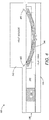
- FIGURE 3 shows a cross-sectional view of a heat dissipation system 100 taken along line A-A of FIGURE 2A .
- the heat dissipation switch 106 is sandwiched between the heat source 102 and the heat sink 104.
- This view illustrates an example in which the thermally switched conductive elements 206 are positioned within the conductive element cavities 204 of the thermally isolating material 202.
- the thermally switched conductive element 206 is shown in an un-actuated configuration in which there is no heat flow path created by the heat dissipation switch 106 between the heat source 102 and the heat sink 104.
- the thermally switched conductive elements 206 in FIGURE 3 are illustrated with two different layers having two different shadings in order to represent a bimetallic material. As discussed above, the thermally switched conductive elements 206 may alternatively include shape memory alloys. Throughout a majority of the remaining figures, the thermally switched conductive elements 206 are depicted without shading or layers for clarity purposes.
- the conductive element cavity 204 is configured with two biasing members 302. These biasing members 302 may be springs or other components that apply a biasing pressure against the thermally switched conductive element 206. The biasing members 302 may accelerate or decelerate activation or deactivation of the corresponding thermally switched conductive element 206. It should be appreciated that the heat dissipation switches 106 of this disclosure are not limited to the use or placement of the biasing members 302. For example, there may additionally or alternatively be biasing members 302 positioned to engage a top surface of the thermally switched conductive element 206 facing the heat source 102.
- FIGURE 4 shows the heat dissipation system 100 of FIGURE 3 with the thermally switched conductive element 206 of the heat dissipation switch 106 configured in an actuated configuration.
- the thermally switched conductive element 206 deforms in response to an increase in temperature, the thermally switched conductive element 206 contacts the surface of the heat source 102 and the surface of the heat sink 104 to create heat flow paths 402 for transferring excess heat from the heat source 102 to the heat sink 104.
- the thermally switched conductive element 206 will deactivate and return to its original un-actuated shape, breaking the contact with the heat source 102 and heat sink 104 to interrupt the heat flow paths 402.
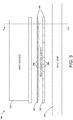
- FIGURE 5 is an exploded side view of a heat dissipation system 100 according to various embodiments in which the heat dissipation switch 106 includes a layer of thermally isolating material 202 and a thermally switched sheet 502 of conductive elements 206.
- the embodiments of the heat dissipation switch 106 discussed above with respect to FIGURES 2-4 utilized a single layer of thermally isolating material 202 with individual thermally switched conductive elements 206 that are not coupled to one another, but rather nested generally unsecured within the conductive element cavities 204 of the thermally isolating material 202.
- the heat dissipation switch 106 includes a layer of thermally isolating material 202 and a thermally switched sheet 502 of conductive elements positioned on a top surface of the thermally isolating material 202.
- the thermally switched sheet 502 includes a number of thermally switched conductive elements 206 that are thermally coupled to one another and nest within the conductive element cavities 204 of the thermally isolating material 202.
- the thermally switched sheet 502 may be manufactured from bimetallic material or shape memory alloy with the thermally switched conductive elements 206 stamped into the desired shape from the sheet of material.
- the thermally switched conductive elements 206 of bimetallic or shape memory alloy may be bonded to a metallic sheet or sheet of any suitable material having a thermal conductivity conducive to produce a heat flow path between the heat source 102 and the heat sink 104 when the thermally switched conductive elements 206 are activated.
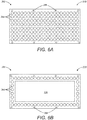
- FIGURES 6A and 6B show top views of a layer of thermally isolating material 202 configured according to a surface mount configuration 210 and an edge mount configuration 220, respectively.
- the thermally isolating material 202 includes a number of conductive element cavities 204 in which the thermally switched conductive elements 206 of the thermally switched sheet 502 will nest.
- FIGURES 7A and 7B show top views of a thermally switched sheet configured according to a surface mount configuration 210 and an edge mount configuration 220, respectively.
- the thermally switched sheet 502 may include any number of thermally switched conductive elements 206 coupled to one another and configured to nest within the corresponding conductive element cavities 204 of the adjacent thermally isolating material 202.
- the thermally switched sheet 502 may be adhesively bonded to the surface of the heat source 102 to be cooled. According to alternative embodiments, the thermally switched sheet 502, as well as the thermally isolating material 202, may be coupled to the heat source 102 using fasteners or other suitable means via mounting apertures 208.
- FIGURE 8 shows a cross-sectional view of a heat dissipation system 100 taken along line A-A of FIGURE 5 with the thermally switched conductive element 206 of the heat dissipation switch 106 configured in an un-actuated configuration.
- FIGURE 9 shows a similar system, but with the thermally switched conductive element 206 configured in an actuated configuration.
- the thermally switched conductive elements 206 were described and shown as being configured to deform in response to an increase in temperature in order to expand outwards beyond the surfaces of the thermally isolating material 202 to create the heat flow paths 402. Essentially an increase in temperature beyond a threshold temperature associated with the material of the thermally switched conductive elements 206 would trigger a change in the elements from a first state that breaks any heat flow paths 402 to a second state that creates the heat flow paths 402. Conversely, in the embodiments discussed above, the thermally switched conductive elements 206 were described and shown as being configured to react to a decrease in temperature through the threshold temperature to return from the second state to the first state, effectively interrupting the heat flow paths 402.
- the embodiment shown in FIGURE 8 may be used to illustrate a heat dissipation switch 106 having the opposite response to temperature increases and decreases to provide identical results.
- the thermally switched conductive element 206 shown in FIGURE 8 may be configured such that when undeformed (i.e., no or minimal internal stress within bimetallic elements), the thermally switched conductive element 206 extends through the thermally isolating material 202 to contact the heat sink 104 and create the heat flow paths 402.
- the thermally switched conductive element 206 is shown with a vent hole 802, which may optionally be placed within the material of the thermally switched conductive element 206 to vent the space of the conductive element cavity 204 between the heat source 102 and the thermally switched conductive element 206.
- the thermally switched conductive element 206 activates to deform from the first state shown in FIGURE 8 to a second state shown in FIGURE 9 in which the thermally switched conductive element 206 displaces away from the heat sink 104 and the conductive element cavity 204. It should be appreciated that according to various embodiments, the precise shape of the thermally switched conductive elements 206 may vary.
- the thermally switched conductive elements 206 may be substantially disk-shaped, projecting away from the thermally switched sheet 502, while according to other embodiments as shown in FIGURE 9 , the thermally switched conductive elements 206 may be configured to be substantially flush with or even recessed from a surface of the thermally switched sheet 502 when configured to isolate the heat source 102 from the heat sink 104.
- FIGURE 9 shows a contact surface 902 configured according to the desired interface between the thermally switched conductive element 206 and the heat sink 104, as will be described below with respect to FIGURE 10 .
- the precise configuration of the thermally switched conductive elements 206 and corresponding contact surface 902 depends on the desired characteristics associated with the specific implementation of the heat dissipation switch 106. Examples include, but are not limited to, type of material of the thermally switched sheet 502 and thermally switched conductive elements 206, shape and dimensions of the thermally switched conductive elements 206, thickness of the conductive element cavities 204, desired actuation times and characteristics associated with the displacement of the thermally switched conductive elements 206, and the desired contact pressure between the thermally switched conductive elements 206 and the heat sink 104.
- FIGURES 8 and 9 have been described as corresponding to un-actuated and actuated states, respectively, of the thermally switched conductive elements 206, it should be appreciated that these examples may also be configured in the opposite manner.
- the thermally switched conductive elements 206 may be configured such that FIGURE 8 represents an actuated state of the thermally switched conductive element 206 and FIGURE 9 represents an un-actuated state. In doing so, the thermally switched conductive elements 206 would activate to deform from the un-actuated state of FIGURE 9 to the actuated state of FIGURE 8 upon an increase in temperature past the threshold temperature.
- the heat dissipation switch 106 of this example utilizes a layer of thermally isolating material 202 adjacent to the heat sink 104 and a thermally switched sheet 502 disposed between the layer of thermally isolating material 202 and the heat source 102 such that the thermally switched conductive elements 206 are positioned to nest within the conductive element cavities 204 of the thermally isolating material 202.
- the contact surface 902 of the thermally switched conductive elements 206 may be configured according to the desired interface between the thermally switched conductive elements 206 and the heat sink 104.
- the contact surface 902 has been shaped to create a substantially flat contact surface when the thermally switched conductive elements 206 are deformed to the position in which the contact surface 902 abuts a surface of the heat sink 104. In doing so, the contact area between the two surfaces is increased, which in turn increases the heat flow path 402 to improve the capability of the heat dissipation switch 106 to transfer excess heat from the heat source 102 to the heat sink 104.
- the heat dissipation switch 106 of FIGURE 10 additionally includes one or more supplemental layers 1002 of bimetallic or shape memory alloy material between the thermally switched sheet 502 and the heat source 102.
- These supplemental layers 1002 may include material having varying deformation characteristics than the thermally switched sheet 502.
- the response rate and/or actuation pressure of the thermally switched conductive elements 206 may be modified.
- the supplemental layers 1002 may allow for the buildup of pressure of the thermally switched conductive elements 206 on the heat sink 104, stepping up the pressure incrementally as the temperature increases due to the various characteristics of the materials of the supplemental layers 1002 and the thermally switched sheet 502.
- the supplemental layers 1002 may be added to the entire top surface of the thermally switched sheet 502, or may be localized over a desired subset of thermally switched conductive elements 206 of the thermally switched sheet 502 as desired.
- FIGURE 11 illustrates another implementation of the heat dissipation switch 106 according to various embodiments.
- This example includes a heat dissipation switch 106 having a layer of thermally isolating material 202 and a thermally switched sheet 502, similar to the examples described above.
- the thickness of the thermally isolating material 202 has been increased to provide an increased thermal isolation between the heat source 102 and the heat sink 104.
- Increasing the thickness of the thermally isolating material 202 may correspondingly increase the depth of the conductive element cavities 204 (space shown occupied by reference numbers 1102 and 1104).
- the thermally switched sheet 502 may be configured so that the thermally switched conductive elements 206 project downward into the conductive element cavities 204, with the primary deformation portions 1106 of the thermally switched conductive elements 206 spanning the width of the conductive element cavities 204.
- This configuration may leave an open cylindrical cavity (space shown occupied by reference number 1102) above the primary deformation portions 1106 of the thermally switched conductive elements 206 within the conductive element cavities 204.
- the open cylindrical cavities created by the configuration of the primary deformation portions 1106 of the thermally switched conductive elements 206 may each be filled with a conductive plug 1102 of solid conductive material.
- the conductive plug 1102 may be capable of transferring excess heat from the heat source 102 to the thermally switched conductive elements 206 once the primary deformation portions 1106 make contact with the heat sink 104 to create the heat flow paths 402.
- the conductive plugs 1102 may be sized and shaped to increase the amount of conductive material between the heat source 102 and the heat sink 104 without interfering with the actuation of the primary deformation portions 1106.
- the shape of the conductive plugs 1102 creates a small nonconductive space 1104 between the conductive plugs 1102 and the primary deformation portions.
- the routine 1200 begins at operation 1202, where a layer of thermally isolating material 202 is provided.
- the thermally isolating material 202 may include any number of conductive element cavities 204 arranged according to any desired configuration.
- the thermally isolating material 202 may be configured according to the characteristics of the surface to which the thermally isolating material 202 will be mounted, such as according to a surface mount configuration 210 or an edge mount configuration 220.
- the routine 1200 continues from operation 1202 to operation 1204, where the thermally switched conductive elements 206 are configured and provided as either individual non-coupled elements as shown in FIGURES 2-4 , or as a thermally switched sheet 502 as shown in FIGURES 5-11 .
- Configuring the thermally switched conductive elements 206 may also include selecting a suitable material for the elements, as well as the shape and size of all of the thermally switched conductive elements 206 and/or any subsets of the thermally switched conductive elements 206.
- the routine 1200 continues to operation 1206, where any supplemental layers 1002 may be selected, configured, and added to the heat dissipation switch 106 according to the desired performance characteristics of the thermally switched conductive elements 206 for the particular application of the heat dissipation switch 106.
- the heat dissipation switch 106 may be coupled to the heat source 102 and to the heat sink 104 using adhesives, fasteners, or some combination of these or other known coupling techniques to create the heat dissipation system 100.
- the routine 1200 continues to operation 1210, where the heat dissipation switch 106 is exposed to increasing or decreasing temperatures to selectively activate or deactivate the switch in order to create or interrupt the heat flow paths 402 for controlling the dissipation of excess heat created by the heat source 102.
Landscapes
- Engineering & Computer Science (AREA)
- Physics & Mathematics (AREA)
- Thermal Sciences (AREA)
- Mechanical Engineering (AREA)
- General Engineering & Computer Science (AREA)
- Condensed Matter Physics & Semiconductors (AREA)
- General Physics & Mathematics (AREA)
- Computer Hardware Design (AREA)
- Microelectronics & Electronic Packaging (AREA)
- Power Engineering (AREA)
- Cooling Or The Like Of Electrical Apparatus (AREA)
- Cooling Or The Like Of Semiconductors Or Solid State Devices (AREA)
Applications Claiming Priority (1)
| Application Number | Priority Date | Filing Date | Title |
|---|---|---|---|
| US13/477,414 US9080820B2 (en) | 2012-05-22 | 2012-05-22 | Heat dissipation switch |
Publications (3)
| Publication Number | Publication Date |
|---|---|
| EP2667141A2 EP2667141A2 (en) | 2013-11-27 |
| EP2667141A3 EP2667141A3 (en) | 2018-03-14 |
| EP2667141B1 true EP2667141B1 (en) | 2019-10-02 |
Family
ID=48468158
Family Applications (1)
| Application Number | Title | Priority Date | Filing Date |
|---|---|---|---|
| EP13168615.6A Active EP2667141B1 (en) | 2012-05-22 | 2013-05-21 | Heat dissipation switch |
Country Status (4)
| Country | Link |
|---|---|
| US (1) | US9080820B2 (enExample) |
| EP (1) | EP2667141B1 (enExample) |
| JP (1) | JP6223712B2 (enExample) |
| CN (1) | CN103429051B (enExample) |
Families Citing this family (48)
| Publication number | Priority date | Publication date | Assignee | Title |
|---|---|---|---|---|
| US9417013B2 (en) * | 2010-11-12 | 2016-08-16 | Toyota Motor Engineering & Manufacturing North America, Inc. | Heat transfer systems including heat conducting composite materials |
| WO2012140927A1 (ja) * | 2011-04-12 | 2012-10-18 | 日本碍子株式会社 | ヒートフロースイッチ |
| CN103826422B (zh) * | 2014-02-13 | 2016-06-29 | 中国科学院工程热物理研究所 | 微通道冷却装置 |
| CN104853562B (zh) * | 2014-02-19 | 2018-04-27 | 联想(北京)有限公司 | 一种电子设备和气流加速装置 |
| US9827697B2 (en) * | 2014-08-29 | 2017-11-28 | The Boeing Company | Systems and methods for curing complex fiber-reinforced composite structures |
| DE112015004475T5 (de) * | 2014-09-30 | 2017-06-14 | Panasonic Intellectual Property Management Co., Ltd. | Platteneinheit |
| US20160266621A1 (en) * | 2015-03-13 | 2016-09-15 | Microsoft Technology Licensing, Llc | Electronic device cooling |
| US10330400B2 (en) * | 2015-03-17 | 2019-06-25 | Toyota Motor Engineering & Manufacturing North America, Inc. | Self-assembled or reconfigurable structures for heat flow control devices |
| US10267578B2 (en) * | 2015-08-04 | 2019-04-23 | Raytheon Company | Shape memory material based thermal coupler/decoupler and method |
| FR3045012B1 (fr) * | 2015-12-11 | 2017-12-08 | Airbus Operations Sas | Mat d'accrochage d'une turbomachine muni d'un element de protection thermique |
| CN106973543A (zh) * | 2016-01-14 | 2017-07-21 | 中兴通讯股份有限公司 | 一种自调节高低温保护装置 |
| JP6274246B2 (ja) * | 2016-04-08 | 2018-02-07 | 株式会社デンソー | 監視装置 |
| KR102701849B1 (ko) * | 2017-01-26 | 2024-09-02 | 삼성전자주식회사 | 적응적 열 저항 및 열 용량을 사용하는 열 관리 장치 및 방법 |
| US10427934B1 (en) * | 2017-03-23 | 2019-10-01 | United States Of America As Represented By The Secretary Of The Air Force | Thermal management using microelectromechanical systems bimorph cantilever beams |
| US10730645B2 (en) | 2017-04-21 | 2020-08-04 | The Boeing Company | System and method for shape memory alloy thermal interface |
| CN106993399A (zh) * | 2017-05-26 | 2017-07-28 | 北京小米移动软件有限公司 | 导热装置 |
| JP6950933B2 (ja) | 2017-07-14 | 2021-10-13 | 国立研究開発法人宇宙航空研究開発機構 | 熱応動アクチュエータおよび熱応動アクチュエータユニット |
| CN107863685A (zh) * | 2017-11-29 | 2018-03-30 | 西安炬光科技股份有限公司 | 一种温度控制结构及激光器模块 |
| US10292307B1 (en) * | 2018-01-04 | 2019-05-14 | Juniper Networks, Inc. | Thermal heatsink |
| CA3101652A1 (en) * | 2018-03-01 | 2019-09-06 | Universitat De Lleida | Deformable fin heat exchanger |
| FR3079021B1 (fr) * | 2018-03-16 | 2020-09-11 | Alstom Transp Tech | Dispositif de conduction thermique et systeme de dissipation de chaleur associe |
| CN108870791A (zh) * | 2018-04-26 | 2018-11-23 | 浙江大学 | 一种采用形状记忆合金的接触式冷却系统 |
| GB2581998B (en) * | 2019-03-07 | 2021-07-28 | Dualitas Ltd | Thermal management of display device |
| US11076504B2 (en) | 2019-03-08 | 2021-07-27 | Appleton Grp Llc | Arrangement for dissipating heat of a power supply unit in a housing |
| JP7354689B2 (ja) * | 2019-08-28 | 2023-10-03 | 大日本印刷株式会社 | 熱伝導率制御体 |
| JP7451912B2 (ja) * | 2019-09-19 | 2024-03-19 | 大日本印刷株式会社 | 構造物 |
| JP7415396B2 (ja) * | 2019-09-26 | 2024-01-17 | 大日本印刷株式会社 | 保温容器 |
| JP7363579B2 (ja) * | 2020-03-02 | 2023-10-18 | 大日本印刷株式会社 | 熱伝導率制御体、隔壁、および構造物 |
| US11204206B2 (en) | 2020-05-18 | 2021-12-21 | Envertic Thermal Systems, Llc | Thermal switch |
| RU2736012C1 (ru) * | 2020-06-20 | 2020-11-11 | Сергей Сергеевич Примаков | Способ регулирования теплопередачи между преимущественно твердым основанием и внешней средой |
| US11493551B2 (en) | 2020-06-22 | 2022-11-08 | Advantest Test Solutions, Inc. | Integrated test cell using active thermal interposer (ATI) with parallel socket actuation |
| US11549981B2 (en) | 2020-10-01 | 2023-01-10 | Advantest Test Solutions, Inc. | Thermal solution for massively parallel testing |
| CN112636163A (zh) * | 2020-10-09 | 2021-04-09 | 金雷 | 一种电子器件的温控装置 |
| US11821913B2 (en) | 2020-11-02 | 2023-11-21 | Advantest Test Solutions, Inc. | Shielded socket and carrier for high-volume test of semiconductor devices |
| US11808812B2 (en) | 2020-11-02 | 2023-11-07 | Advantest Test Solutions, Inc. | Passive carrier-based device delivery for slot-based high-volume semiconductor test system |
| US12320841B2 (en) | 2020-11-19 | 2025-06-03 | Advantest Test Solutions, Inc. | Wafer scale active thermal interposer for device testing |
| US11567119B2 (en) | 2020-12-04 | 2023-01-31 | Advantest Test Solutions, Inc. | Testing system including active thermal interposer device |
| US11573262B2 (en) | 2020-12-31 | 2023-02-07 | Advantest Test Solutions, Inc. | Multi-input multi-zone thermal control for device testing |
| US11587640B2 (en) | 2021-03-08 | 2023-02-21 | Advantest Test Solutions, Inc. | Carrier based high volume system level testing of devices with pop structures |
| US12235314B2 (en) | 2021-09-14 | 2025-02-25 | Advantest Test Solutions, Inc | Parallel test cell with self actuated sockets |
| US11656273B1 (en) | 2021-11-05 | 2023-05-23 | Advantest Test Solutions, Inc. | High current device testing apparatus and systems |
| DE102022100684B3 (de) | 2022-01-13 | 2023-06-07 | Audi Aktiengesellschaft | Thermisches Koppelelement |
| US11835549B2 (en) | 2022-01-26 | 2023-12-05 | Advantest Test Solutions, Inc. | Thermal array with gimbal features and enhanced thermal performance |
| US12411167B2 (en) | 2022-01-26 | 2025-09-09 | Advantest Test Solutions, Inc. | Tension-based socket gimbal for engaging device under test with thermal array |
| US12339075B2 (en) | 2022-03-01 | 2025-06-24 | Toyota Motor Engineering & Manufacturing North America, Inc. | Bi-functional thermal cooling systems and methods thereof |
| CN114593623B (zh) * | 2022-03-30 | 2023-10-20 | 内蒙古工业大学 | 一种可自动调整换热面积的换热器 |
| CN117420896A (zh) * | 2022-07-11 | 2024-01-19 | 戴尔产品有限公司 | 用于使用温度测量对计算装置进行热管理的系统和方法 |
| IL309141A (en) * | 2023-12-06 | 2025-07-01 | Israel Aerospace Ind Ltd | Heat transfer arrangement |
Family Cites Families (29)
| Publication number | Priority date | Publication date | Assignee | Title |
|---|---|---|---|---|
| US3519067A (en) * | 1967-12-28 | 1970-07-07 | Honeywell Inc | Variable thermal conductance devices |
| US4304294A (en) | 1978-08-17 | 1981-12-08 | Ford Aerospace & Communications Corp. | Thermal energy switch |
| JPS6235547A (ja) * | 1985-08-08 | 1987-02-16 | Nec Corp | 半導体素子の冷却機構 |
| US4742867A (en) * | 1986-12-01 | 1988-05-10 | Cape Cod Research, Inc. | Method and apparatuses for heat transfer |
| US5131456A (en) * | 1991-07-01 | 1992-07-21 | Ibm Corporation | Bimetallic insert fin for high conduction cooling structure |
| JPH05259667A (ja) * | 1992-03-13 | 1993-10-08 | Fujitsu Ltd | 放熱構造 |
| DE69328687D1 (de) * | 1993-07-06 | 2000-06-21 | Toshiba Kawasaki Kk | Wärmeleitende platte |
| JPH07210257A (ja) * | 1994-01-17 | 1995-08-11 | Hitachi Ltd | 熱流路可変表面を用いた温度制御装置 |
| JPH11351679A (ja) * | 1998-06-10 | 1999-12-24 | Nikkiso Co Ltd | 冷却装置 |
| US6608752B2 (en) * | 2001-09-24 | 2003-08-19 | General Electric Company | Adaptive heat sink for electronics applications |
| JP2003110185A (ja) * | 2001-10-02 | 2003-04-11 | Toshiba Corp | 光通信モジュール |
| US20050074666A1 (en) * | 2002-08-29 | 2005-04-07 | Hirokazu Kimiya | Heat control device for battery |
| US7411792B2 (en) * | 2002-11-18 | 2008-08-12 | Washington State University Research Foundation | Thermal switch, methods of use and manufacturing methods for same |
| CN100370604C (zh) * | 2004-04-15 | 2008-02-20 | 鸿富锦精密工业(深圳)有限公司 | 一种热界面材料及其制造方法 |
| US20060141308A1 (en) * | 2004-12-23 | 2006-06-29 | Becerra Juan J | Apparatus and method for variable conductance temperature control |
| US20070205473A1 (en) * | 2006-03-03 | 2007-09-06 | Honeywell International Inc. | Passive analog thermal isolation structure |
| FR2899374B1 (fr) * | 2006-03-30 | 2008-05-30 | Air Liquide | Interrupteur thermique |
| US20070241635A1 (en) * | 2006-04-17 | 2007-10-18 | Multispectral Imaging, Inc. | Apparatus Comprising a Thermal Bimorph with Enhanced Sensitivity |
| JP4648351B2 (ja) * | 2007-03-30 | 2011-03-09 | 住友ベークライト株式会社 | 伝熱シートおよび放熱構造体 |
| US7752866B2 (en) * | 2007-12-07 | 2010-07-13 | University Of Central Florida Research Foundation, Inc. | Shape memory thermal conduction switch |
| US20090218087A1 (en) * | 2008-02-29 | 2009-09-03 | Denso Corporation | Thermal conduction structure, composite material, and method of producing the material |
| JP2009203441A (ja) * | 2008-02-29 | 2009-09-10 | Denso Corp | コンポジット材料、その製造方法、及び複合構造体 |
| US20090321044A1 (en) * | 2008-06-30 | 2009-12-31 | Alcatel-Lucent Technologies Inc. | Active heat sink designs |
| US20100021678A1 (en) * | 2008-07-23 | 2010-01-28 | Tai-Her Yang | Thermal conduction principle and device for intercrossed structure having different thermal characteristics |
| CN101458050A (zh) * | 2008-12-22 | 2009-06-17 | 中国航天科技集团公司第五研究院第五一○研究所 | 一种可变散热器及其制作方法 |
| US8215377B1 (en) * | 2009-05-06 | 2012-07-10 | Lockheed Martin Corporation | Heat transfer device with flexible cooling layer |
| US20110168378A1 (en) * | 2010-01-14 | 2011-07-14 | Irvine Sensors Corporation | Thermal power distribution system |
| US8659903B2 (en) * | 2011-12-06 | 2014-02-25 | Palo Alto Research Center Incorporated | Heat switch array for thermal hot spot cooling |
| CN102594289A (zh) * | 2012-01-31 | 2012-07-18 | 华为终端有限公司 | 热敏感器件及其散热系统 |
-
2012
- 2012-05-22 US US13/477,414 patent/US9080820B2/en active Active
-
2013
- 2013-05-16 CN CN201310182259.8A patent/CN103429051B/zh active Active
- 2013-05-21 EP EP13168615.6A patent/EP2667141B1/en active Active
- 2013-05-21 JP JP2013106746A patent/JP6223712B2/ja active Active
Also Published As
| Publication number | Publication date |
|---|---|
| EP2667141A3 (en) | 2018-03-14 |
| JP2013243365A (ja) | 2013-12-05 |
| CN103429051A (zh) | 2013-12-04 |
| CN103429051B (zh) | 2017-08-08 |
| US20130314202A1 (en) | 2013-11-28 |
| US9080820B2 (en) | 2015-07-14 |
| JP6223712B2 (ja) | 2017-11-01 |
| EP2667141A2 (en) | 2013-11-27 |
Similar Documents
| Publication | Publication Date | Title |
|---|---|---|
| EP2667141B1 (en) | Heat dissipation switch | |
| US11075331B2 (en) | Thermoelectric device having circuitry with structural rigidity | |
| JP2013243365A5 (enExample) | ||
| EP1993135B1 (en) | Heat conducter | |
| US7090001B2 (en) | Optimized multiple heat pipe blocks for electronics cooling | |
| EP2758729B1 (en) | Layer assembly for heat exchanger | |
| US20080099193A1 (en) | Self-regulated cooling mechanism | |
| US10477728B2 (en) | Apparatus, system, and method for cooling devices containing multiple components | |
| CN110364501B (zh) | 一种微流道散热结构、制造方法及电子器件 | |
| EP3410831B1 (en) | Thermal separation of electronic control chassis heatsinks fins | |
| JP7714701B2 (ja) | 電池アセンブリ、電池パック及び車両 | |
| JP2018522407A (ja) | 車両バッテリ用の熱的隔離特徴を備える熱電モジュール | |
| KR20120026980A (ko) | 열 저항을 감소시키기 위한 열 인터페이스 물질 및 이의 제조 방법 | |
| EP1831936B1 (en) | Piezoelectric bimorph actuator and method of manufacturing thereof | |
| CN108990369A (zh) | 具有高温和低温区域冷却系统的电力电子器件的系统和方法 | |
| EP4402417B1 (en) | Phase change material (pcm)-based conductive thermal actuator switch | |
| US20030183371A1 (en) | Heat sink | |
| EP3336891B1 (en) | Pressure limiting heat sink | |
| JP5166705B2 (ja) | 熱電発電装置 | |
| US20180108591A1 (en) | Semiconductor device | |
| EP2966681A1 (en) | Power semiconductor devices | |
| US20250040104A1 (en) | Housing for an electronic circuit | |
| KR20250040716A (ko) | 상 변화 물질(pcm) 기반 전도성 열 액추에이터 스위치들 및 관련된 적층 및 배열 시스템 | |
| JP2001210983A (ja) | 熱抵抗制御装置 | |
| KR200296515Y1 (ko) | 열전모듈의 열효율을 증대시키기 위한 장치 |
Legal Events
| Date | Code | Title | Description |
|---|---|---|---|
| PUAI | Public reference made under article 153(3) epc to a published international application that has entered the european phase |
Free format text: ORIGINAL CODE: 0009012 |
|
| AK | Designated contracting states |
Kind code of ref document: A2 Designated state(s): AL AT BE BG CH CY CZ DE DK EE ES FI FR GB GR HR HU IE IS IT LI LT LU LV MC MK MT NL NO PL PT RO RS SE SI SK SM TR |
|
| AX | Request for extension of the european patent |
Extension state: BA ME |
|
| PUAL | Search report despatched |
Free format text: ORIGINAL CODE: 0009013 |
|
| AK | Designated contracting states |
Kind code of ref document: A3 Designated state(s): AL AT BE BG CH CY CZ DE DK EE ES FI FR GB GR HR HU IE IS IT LI LT LU LV MC MK MT NL NO PL PT RO RS SE SI SK SM TR |
|
| AX | Request for extension of the european patent |
Extension state: BA ME |
|
| RIC1 | Information provided on ipc code assigned before grant |
Ipc: H01L 23/36 20060101ALI20180206BHEP Ipc: H05K 7/20 20060101ALI20180206BHEP Ipc: F28F 13/00 20060101AFI20180206BHEP |
|
| STAA | Information on the status of an ep patent application or granted ep patent |
Free format text: STATUS: REQUEST FOR EXAMINATION WAS MADE |
|
| 17P | Request for examination filed |
Effective date: 20180824 |
|
| RBV | Designated contracting states (corrected) |
Designated state(s): AL AT BE BG CH CY CZ DE DK EE ES FI FR GB GR HR HU IE IS IT LI LT LU LV MC MK MT NL NO PL PT RO RS SE SI SK SM TR |
|
| GRAP | Despatch of communication of intention to grant a patent |
Free format text: ORIGINAL CODE: EPIDOSNIGR1 |
|
| STAA | Information on the status of an ep patent application or granted ep patent |
Free format text: STATUS: GRANT OF PATENT IS INTENDED |
|
| INTG | Intention to grant announced |
Effective date: 20190423 |
|
| GRAS | Grant fee paid |
Free format text: ORIGINAL CODE: EPIDOSNIGR3 |
|
| GRAA | (expected) grant |
Free format text: ORIGINAL CODE: 0009210 |
|
| STAA | Information on the status of an ep patent application or granted ep patent |
Free format text: STATUS: THE PATENT HAS BEEN GRANTED |
|
| AK | Designated contracting states |
Kind code of ref document: B1 Designated state(s): AL AT BE BG CH CY CZ DE DK EE ES FI FR GB GR HR HU IE IS IT LI LT LU LV MC MK MT NL NO PL PT RO RS SE SI SK SM TR |
|
| REG | Reference to a national code |
Ref country code: GB Ref legal event code: FG4D |
|
| REG | Reference to a national code |
Ref country code: CH Ref legal event code: EP Ref country code: AT Ref legal event code: REF Ref document number: 1186659 Country of ref document: AT Kind code of ref document: T Effective date: 20191015 |
|
| REG | Reference to a national code |
Ref country code: DE Ref legal event code: R096 Ref document number: 602013061168 Country of ref document: DE |
|
| REG | Reference to a national code |
Ref country code: IE Ref legal event code: FG4D |
|
| REG | Reference to a national code |
Ref country code: DE Ref legal event code: R082 Ref document number: 602013061168 Country of ref document: DE Representative=s name: MAIER, LL.M., MICHAEL C., DE Ref country code: DE Ref legal event code: R082 Ref document number: 602013061168 Country of ref document: DE Representative=s name: BOULT WADE TENNANT LLP, DE |
|
| REG | Reference to a national code |
Ref country code: NL Ref legal event code: MP Effective date: 20191002 |
|
| REG | Reference to a national code |
Ref country code: DE Ref legal event code: R082 Ref document number: 602013061168 Country of ref document: DE Representative=s name: BOULT WADE TENNANT LLP, DE |
|
| REG | Reference to a national code |
Ref country code: LT Ref legal event code: MG4D |
|
| REG | Reference to a national code |
Ref country code: AT Ref legal event code: MK05 Ref document number: 1186659 Country of ref document: AT Kind code of ref document: T Effective date: 20191002 |
|
| PG25 | Lapsed in a contracting state [announced via postgrant information from national office to epo] |
Ref country code: ES Free format text: LAPSE BECAUSE OF FAILURE TO SUBMIT A TRANSLATION OF THE DESCRIPTION OR TO PAY THE FEE WITHIN THE PRESCRIBED TIME-LIMIT Effective date: 20191002 Ref country code: SE Free format text: LAPSE BECAUSE OF FAILURE TO SUBMIT A TRANSLATION OF THE DESCRIPTION OR TO PAY THE FEE WITHIN THE PRESCRIBED TIME-LIMIT Effective date: 20191002 Ref country code: LV Free format text: LAPSE BECAUSE OF FAILURE TO SUBMIT A TRANSLATION OF THE DESCRIPTION OR TO PAY THE FEE WITHIN THE PRESCRIBED TIME-LIMIT Effective date: 20191002 Ref country code: AT Free format text: LAPSE BECAUSE OF FAILURE TO SUBMIT A TRANSLATION OF THE DESCRIPTION OR TO PAY THE FEE WITHIN THE PRESCRIBED TIME-LIMIT Effective date: 20191002 Ref country code: FI Free format text: LAPSE BECAUSE OF FAILURE TO SUBMIT A TRANSLATION OF THE DESCRIPTION OR TO PAY THE FEE WITHIN THE PRESCRIBED TIME-LIMIT Effective date: 20191002 Ref country code: BG Free format text: LAPSE BECAUSE OF FAILURE TO SUBMIT A TRANSLATION OF THE DESCRIPTION OR TO PAY THE FEE WITHIN THE PRESCRIBED TIME-LIMIT Effective date: 20200102 Ref country code: PT Free format text: LAPSE BECAUSE OF FAILURE TO SUBMIT A TRANSLATION OF THE DESCRIPTION OR TO PAY THE FEE WITHIN THE PRESCRIBED TIME-LIMIT Effective date: 20200203 Ref country code: NO Free format text: LAPSE BECAUSE OF FAILURE TO SUBMIT A TRANSLATION OF THE DESCRIPTION OR TO PAY THE FEE WITHIN THE PRESCRIBED TIME-LIMIT Effective date: 20200102 Ref country code: PL Free format text: LAPSE BECAUSE OF FAILURE TO SUBMIT A TRANSLATION OF THE DESCRIPTION OR TO PAY THE FEE WITHIN THE PRESCRIBED TIME-LIMIT Effective date: 20191002 Ref country code: NL Free format text: LAPSE BECAUSE OF FAILURE TO SUBMIT A TRANSLATION OF THE DESCRIPTION OR TO PAY THE FEE WITHIN THE PRESCRIBED TIME-LIMIT Effective date: 20191002 Ref country code: LT Free format text: LAPSE BECAUSE OF FAILURE TO SUBMIT A TRANSLATION OF THE DESCRIPTION OR TO PAY THE FEE WITHIN THE PRESCRIBED TIME-LIMIT Effective date: 20191002 Ref country code: GR Free format text: LAPSE BECAUSE OF FAILURE TO SUBMIT A TRANSLATION OF THE DESCRIPTION OR TO PAY THE FEE WITHIN THE PRESCRIBED TIME-LIMIT Effective date: 20200103 |
|
| PG25 | Lapsed in a contracting state [announced via postgrant information from national office to epo] |
Ref country code: RS Free format text: LAPSE BECAUSE OF FAILURE TO SUBMIT A TRANSLATION OF THE DESCRIPTION OR TO PAY THE FEE WITHIN THE PRESCRIBED TIME-LIMIT Effective date: 20191002 Ref country code: HR Free format text: LAPSE BECAUSE OF FAILURE TO SUBMIT A TRANSLATION OF THE DESCRIPTION OR TO PAY THE FEE WITHIN THE PRESCRIBED TIME-LIMIT Effective date: 20191002 Ref country code: CZ Free format text: LAPSE BECAUSE OF FAILURE TO SUBMIT A TRANSLATION OF THE DESCRIPTION OR TO PAY THE FEE WITHIN THE PRESCRIBED TIME-LIMIT Effective date: 20191002 Ref country code: IS Free format text: LAPSE BECAUSE OF FAILURE TO SUBMIT A TRANSLATION OF THE DESCRIPTION OR TO PAY THE FEE WITHIN THE PRESCRIBED TIME-LIMIT Effective date: 20200224 |
|
| PG25 | Lapsed in a contracting state [announced via postgrant information from national office to epo] |
Ref country code: AL Free format text: LAPSE BECAUSE OF FAILURE TO SUBMIT A TRANSLATION OF THE DESCRIPTION OR TO PAY THE FEE WITHIN THE PRESCRIBED TIME-LIMIT Effective date: 20191002 |
|
| REG | Reference to a national code |
Ref country code: DE Ref legal event code: R097 Ref document number: 602013061168 Country of ref document: DE |
|
| PG2D | Information on lapse in contracting state deleted |
Ref country code: IS |
|
| PG25 | Lapsed in a contracting state [announced via postgrant information from national office to epo] |
Ref country code: RO Free format text: LAPSE BECAUSE OF FAILURE TO SUBMIT A TRANSLATION OF THE DESCRIPTION OR TO PAY THE FEE WITHIN THE PRESCRIBED TIME-LIMIT Effective date: 20191002 Ref country code: EE Free format text: LAPSE BECAUSE OF FAILURE TO SUBMIT A TRANSLATION OF THE DESCRIPTION OR TO PAY THE FEE WITHIN THE PRESCRIBED TIME-LIMIT Effective date: 20191002 Ref country code: DK Free format text: LAPSE BECAUSE OF FAILURE TO SUBMIT A TRANSLATION OF THE DESCRIPTION OR TO PAY THE FEE WITHIN THE PRESCRIBED TIME-LIMIT Effective date: 20191002 Ref country code: IS Free format text: LAPSE BECAUSE OF FAILURE TO SUBMIT A TRANSLATION OF THE DESCRIPTION OR TO PAY THE FEE WITHIN THE PRESCRIBED TIME-LIMIT Effective date: 20200202 |
|
| PLBE | No opposition filed within time limit |
Free format text: ORIGINAL CODE: 0009261 |
|
| STAA | Information on the status of an ep patent application or granted ep patent |
Free format text: STATUS: NO OPPOSITION FILED WITHIN TIME LIMIT |
|
| PG25 | Lapsed in a contracting state [announced via postgrant information from national office to epo] |
Ref country code: SK Free format text: LAPSE BECAUSE OF FAILURE TO SUBMIT A TRANSLATION OF THE DESCRIPTION OR TO PAY THE FEE WITHIN THE PRESCRIBED TIME-LIMIT Effective date: 20191002 Ref country code: IT Free format text: LAPSE BECAUSE OF FAILURE TO SUBMIT A TRANSLATION OF THE DESCRIPTION OR TO PAY THE FEE WITHIN THE PRESCRIBED TIME-LIMIT Effective date: 20191002 Ref country code: SM Free format text: LAPSE BECAUSE OF FAILURE TO SUBMIT A TRANSLATION OF THE DESCRIPTION OR TO PAY THE FEE WITHIN THE PRESCRIBED TIME-LIMIT Effective date: 20191002 |
|
| 26N | No opposition filed |
Effective date: 20200703 |
|
| PG25 | Lapsed in a contracting state [announced via postgrant information from national office to epo] |
Ref country code: SI Free format text: LAPSE BECAUSE OF FAILURE TO SUBMIT A TRANSLATION OF THE DESCRIPTION OR TO PAY THE FEE WITHIN THE PRESCRIBED TIME-LIMIT Effective date: 20191002 |
|
| PG25 | Lapsed in a contracting state [announced via postgrant information from national office to epo] |
Ref country code: CH Free format text: LAPSE BECAUSE OF NON-PAYMENT OF DUE FEES Effective date: 20200531 Ref country code: LI Free format text: LAPSE BECAUSE OF NON-PAYMENT OF DUE FEES Effective date: 20200531 Ref country code: MC Free format text: LAPSE BECAUSE OF FAILURE TO SUBMIT A TRANSLATION OF THE DESCRIPTION OR TO PAY THE FEE WITHIN THE PRESCRIBED TIME-LIMIT Effective date: 20191002 |
|
| REG | Reference to a national code |
Ref country code: BE Ref legal event code: MM Effective date: 20200531 |
|
| PG25 | Lapsed in a contracting state [announced via postgrant information from national office to epo] |
Ref country code: LU Free format text: LAPSE BECAUSE OF NON-PAYMENT OF DUE FEES Effective date: 20200521 |
|
| PG25 | Lapsed in a contracting state [announced via postgrant information from national office to epo] |
Ref country code: IE Free format text: LAPSE BECAUSE OF NON-PAYMENT OF DUE FEES Effective date: 20200521 |
|
| PG25 | Lapsed in a contracting state [announced via postgrant information from national office to epo] |
Ref country code: BE Free format text: LAPSE BECAUSE OF NON-PAYMENT OF DUE FEES Effective date: 20200531 |
|
| PG25 | Lapsed in a contracting state [announced via postgrant information from national office to epo] |
Ref country code: TR Free format text: LAPSE BECAUSE OF FAILURE TO SUBMIT A TRANSLATION OF THE DESCRIPTION OR TO PAY THE FEE WITHIN THE PRESCRIBED TIME-LIMIT Effective date: 20191002 Ref country code: MT Free format text: LAPSE BECAUSE OF FAILURE TO SUBMIT A TRANSLATION OF THE DESCRIPTION OR TO PAY THE FEE WITHIN THE PRESCRIBED TIME-LIMIT Effective date: 20191002 Ref country code: CY Free format text: LAPSE BECAUSE OF FAILURE TO SUBMIT A TRANSLATION OF THE DESCRIPTION OR TO PAY THE FEE WITHIN THE PRESCRIBED TIME-LIMIT Effective date: 20191002 |
|
| PG25 | Lapsed in a contracting state [announced via postgrant information from national office to epo] |
Ref country code: MK Free format text: LAPSE BECAUSE OF FAILURE TO SUBMIT A TRANSLATION OF THE DESCRIPTION OR TO PAY THE FEE WITHIN THE PRESCRIBED TIME-LIMIT Effective date: 20191002 |
|
| P01 | Opt-out of the competence of the unified patent court (upc) registered |
Effective date: 20230516 |
|
| PGFP | Annual fee paid to national office [announced via postgrant information from national office to epo] |
Ref country code: DE Payment date: 20250529 Year of fee payment: 13 |
|
| PGFP | Annual fee paid to national office [announced via postgrant information from national office to epo] |
Ref country code: GB Payment date: 20250527 Year of fee payment: 13 |
|
| PGFP | Annual fee paid to national office [announced via postgrant information from national office to epo] |
Ref country code: FR Payment date: 20250526 Year of fee payment: 13 |