EP2665100A2 - Lichtemittierende Diodenanzeige und Verfahren zu deren Herstellung - Google Patents
Lichtemittierende Diodenanzeige und Verfahren zu deren Herstellung Download PDFInfo
- Publication number
- EP2665100A2 EP2665100A2 EP13167655.3A EP13167655A EP2665100A2 EP 2665100 A2 EP2665100 A2 EP 2665100A2 EP 13167655 A EP13167655 A EP 13167655A EP 2665100 A2 EP2665100 A2 EP 2665100A2
- Authority
- EP
- European Patent Office
- Prior art keywords
- light
- emitting
- ingan
- doped
- nanorod
- Prior art date
- Legal status (The legal status is an assumption and is not a legal conclusion. Google has not performed a legal analysis and makes no representation as to the accuracy of the status listed.)
- Withdrawn
Links
Images


Classifications
-
- H—ELECTRICITY
- H01—ELECTRIC ELEMENTS
- H01L—SEMICONDUCTOR DEVICES NOT COVERED BY CLASS H10
- H01L27/00—Devices consisting of a plurality of semiconductor or other solid-state components formed in or on a common substrate
- H01L27/15—Devices consisting of a plurality of semiconductor or other solid-state components formed in or on a common substrate including semiconductor components with at least one potential-jump barrier or surface barrier specially adapted for light emission
- H01L27/153—Devices consisting of a plurality of semiconductor or other solid-state components formed in or on a common substrate including semiconductor components with at least one potential-jump barrier or surface barrier specially adapted for light emission in a repetitive configuration, e.g. LED bars
- H01L27/156—Devices consisting of a plurality of semiconductor or other solid-state components formed in or on a common substrate including semiconductor components with at least one potential-jump barrier or surface barrier specially adapted for light emission in a repetitive configuration, e.g. LED bars two-dimensional arrays
-
- G—PHYSICS
- G09—EDUCATION; CRYPTOGRAPHY; DISPLAY; ADVERTISING; SEALS
- G09F—DISPLAYING; ADVERTISING; SIGNS; LABELS OR NAME-PLATES; SEALS
- G09F9/00—Indicating arrangements for variable information in which the information is built-up on a support by selection or combination of individual elements
- G09F9/30—Indicating arrangements for variable information in which the information is built-up on a support by selection or combination of individual elements in which the desired character or characters are formed by combining individual elements
- G09F9/33—Indicating arrangements for variable information in which the information is built-up on a support by selection or combination of individual elements in which the desired character or characters are formed by combining individual elements being semiconductor devices, e.g. diodes
-
- H—ELECTRICITY
- H01—ELECTRIC ELEMENTS
- H01L—SEMICONDUCTOR DEVICES NOT COVERED BY CLASS H10
- H01L33/00—Semiconductor devices with at least one potential-jump barrier or surface barrier specially adapted for light emission; Processes or apparatus specially adapted for the manufacture or treatment thereof or of parts thereof; Details thereof
- H01L33/02—Semiconductor devices with at least one potential-jump barrier or surface barrier specially adapted for light emission; Processes or apparatus specially adapted for the manufacture or treatment thereof or of parts thereof; Details thereof characterised by the semiconductor bodies
- H01L33/04—Semiconductor devices with at least one potential-jump barrier or surface barrier specially adapted for light emission; Processes or apparatus specially adapted for the manufacture or treatment thereof or of parts thereof; Details thereof characterised by the semiconductor bodies with a quantum effect structure or superlattice, e.g. tunnel junction
- H01L33/06—Semiconductor devices with at least one potential-jump barrier or surface barrier specially adapted for light emission; Processes or apparatus specially adapted for the manufacture or treatment thereof or of parts thereof; Details thereof characterised by the semiconductor bodies with a quantum effect structure or superlattice, e.g. tunnel junction within the light emitting region, e.g. quantum confinement structure or tunnel barrier
-
- H—ELECTRICITY
- H01—ELECTRIC ELEMENTS
- H01L—SEMICONDUCTOR DEVICES NOT COVERED BY CLASS H10
- H01L33/00—Semiconductor devices with at least one potential-jump barrier or surface barrier specially adapted for light emission; Processes or apparatus specially adapted for the manufacture or treatment thereof or of parts thereof; Details thereof
- H01L33/02—Semiconductor devices with at least one potential-jump barrier or surface barrier specially adapted for light emission; Processes or apparatus specially adapted for the manufacture or treatment thereof or of parts thereof; Details thereof characterised by the semiconductor bodies
- H01L33/08—Semiconductor devices with at least one potential-jump barrier or surface barrier specially adapted for light emission; Processes or apparatus specially adapted for the manufacture or treatment thereof or of parts thereof; Details thereof characterised by the semiconductor bodies with a plurality of light emitting regions, e.g. laterally discontinuous light emitting layer or photoluminescent region integrated within the semiconductor body
-
- H—ELECTRICITY
- H01—ELECTRIC ELEMENTS
- H01L—SEMICONDUCTOR DEVICES NOT COVERED BY CLASS H10
- H01L33/00—Semiconductor devices with at least one potential-jump barrier or surface barrier specially adapted for light emission; Processes or apparatus specially adapted for the manufacture or treatment thereof or of parts thereof; Details thereof
- H01L33/02—Semiconductor devices with at least one potential-jump barrier or surface barrier specially adapted for light emission; Processes or apparatus specially adapted for the manufacture or treatment thereof or of parts thereof; Details thereof characterised by the semiconductor bodies
- H01L33/16—Semiconductor devices with at least one potential-jump barrier or surface barrier specially adapted for light emission; Processes or apparatus specially adapted for the manufacture or treatment thereof or of parts thereof; Details thereof characterised by the semiconductor bodies with a particular crystal structure or orientation, e.g. polycrystalline, amorphous or porous
- H01L33/18—Semiconductor devices with at least one potential-jump barrier or surface barrier specially adapted for light emission; Processes or apparatus specially adapted for the manufacture or treatment thereof or of parts thereof; Details thereof characterised by the semiconductor bodies with a particular crystal structure or orientation, e.g. polycrystalline, amorphous or porous within the light emitting region
-
- H—ELECTRICITY
- H01—ELECTRIC ELEMENTS
- H01L—SEMICONDUCTOR DEVICES NOT COVERED BY CLASS H10
- H01L33/00—Semiconductor devices with at least one potential-jump barrier or surface barrier specially adapted for light emission; Processes or apparatus specially adapted for the manufacture or treatment thereof or of parts thereof; Details thereof
- H01L33/02—Semiconductor devices with at least one potential-jump barrier or surface barrier specially adapted for light emission; Processes or apparatus specially adapted for the manufacture or treatment thereof or of parts thereof; Details thereof characterised by the semiconductor bodies
- H01L33/26—Materials of the light emitting region
- H01L33/30—Materials of the light emitting region containing only elements of group III and group V of the periodic system
- H01L33/32—Materials of the light emitting region containing only elements of group III and group V of the periodic system containing nitrogen
Definitions
- the present invention relates to light-emitting diode displays and their forming methods.
- LED displays employ red, green, and blue light-emitting diodes functioning as red, green, and blue light-emitting sub-pixels, respectively, and a color image is displayed according to the combination of emissions of these three types of sub-pixels.
- full-color light-emitting diode displays has many challenges to be overcome. For example, a challenge is related to the complicated and costly manufacturing process.
- the light-emitting diodes are typically grown on separate substrates, and they need to be transferred to a display substrate. The transfer is a difficult process due to the vast number of light-emitting diodes. For instance, the number of sub-pixels or the number of the light-emitting diodes of a 40-inch diagonal full HD (high definition) full-color display equals 1920 ⁇ 1080 ⁇ 3. Accordingly, there are 6,220,800 light-emitting diodes needed to be transferred and many of them may fail during the transfer.
- red, green, and blue light-emitting diodes are usually formed in two or three individual substrates. A desired number of red, green, and blue LED diodes are then transferred and mounted to a single package to form a surface-mounted device (SMD), which is then mounted on a printed-circuit board.
- SMD surface-mounted device
- wire-bonding steps are usually needed to electrically connect the light-emitting diodes with the printed-circuit board or the display substrate.
- LED displays Furthermore, the emitting efficiency, brightness, and other properties of LED displays are based on a hybrid approach or typically unsatisfactory.
- An object of the present invention is to provide light-emitting diode displays with improved configuration and manufacturing method.
- An embodiment of this invention provides a light-emitting diode display comprising a substrate and a plurality of pixels arranged on the substrate.
- Each pixel comprises a first, a second, and a third sub-pixel, and each sub-pixel comprises one or more first, second, or third light-emitting diodes for emitting a first, a second, or a third color.
- Each of the first, second, and third light-emitting diode comprises: a first electrode; a first doped nanorod in ohmic contact with the first electrode; an active light-emitting region arranged on the first doped nanorod; a second doped nanorod arranged on the active light-emitting region; and a second electrode arranged on the second doped nanorod.
- Another embodiment of this invention provides a method for producing a light-emitting diode display, the method comprising the steps of (1) providing a conductive substrate; (2) forming a plurality of first doped nanorods on the substrate; (3) forming an integral first electrode or a plurality of individual first electrodes to form ohmic contact with the first doped nanorods via the conductive substrate; (4) forming a first active light-emitting region on each of a plurality of first top surfaces of the first doped nanorods; (5) forming a second active light-emitting region on each of a plurality of second top surfaces of the first doped nanorods; (6) forming a third active light-emitting region on each of a plurality of third top surfaces of the first doped nanorods; (7) forming a second doped nanorod on each of the first, second, and third light-emitting regions; (8) forming a second electrode on each second doped nanorod; wherein the first, second, and third light-emitting
- the primary object of the present invention can be achieved by using self-assembled GaN nanorod arrays on Si substrates as templates for growing strain-free InGaN/GaN nanorod heterostructures.
- the most salient feature of the nanorod-based approach is the absence of piezoelectric polarization effects, allowing thick (tens of nm) InGaN nanodisk emitter structures in the full visible range.
- the present invention demonstrates both monolithic, phosphor-free white (polychromatic) nanorod-array LEDs and polarized full-color (monochromatic) single-nanorod LEDs.
- a phosphor-free white, polychromatic nanorod-array LEDs according to a preferred embodiment is described below.
- Vertically self-aligned GaN nanorod arrays were grown along the wurtzite c-axis on 3-inch, n -type Si(111) substrates by plasma-assisted molecular-beam epitaxy (PAMBE) [ Chen, H.-Y., Lin, H.-W., Shen, C.-H. & Gwo, S. Structure and photoluminescence properties of epitaxially oriented GaN nanorods grown on Si(111) by plasma-assisted molecular-beam epitaxy. Appl. Phys. Lett. 89, 243105 (2006 )].
- the PAMBE-grown GaN nanorod arrays exhibit the properties of strain- and dislocation-free single crystals, which can be used as nanostructured compliant templates for growing strain-free InGaN nanodisks.
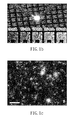
- Figures 1a to 1d show a light-emitting diode according to a preferred embodiment of the present invention, where figure 1a is a schematic diagram of nanorod-array LED structure for generating white light; figure 1b is a photograph of nanorod-array LED emitting white light at 20 mA injection current, and micro-electroluminescence (EL) images shown below are acquired under a 10 ⁇ objective at various injection currents; figure 1c is a micro-EL image (20 mA) under a 100x objective revealing full-visible-spectrum emissions from the white LED shown in the photograph with scale bar: 10 ⁇ m, and figure 1d is Commission international de l'Éclairage (CIE) 1931 chromaticity coordinates at injection currents from 5 mA to 25 mA in which the correlated color temperature (shown on the Planckian locus) maintains at near 6000 K (natural white light) for injection currents larger than 5 mA.
- CIE Commission international de l'Éclairage
- the light-emitting diode of the embodiment primarily includes a n-type silicon substrate 1, a Ti/Au electrode 2 disposed on the silicon substrate 1, a n-type gallium nitride (GaN) nanorod array 3 consisted of n-type GaN nanorods ohmic contact with the Ti/Au electrode 2, one or more indium gallium nitride (InGaN) nanodisks 4 disposed on each of the n-type GaN nanorod 3, a p-type GaN nanorod array 5 consisted of p-type GaN nanorods disposed on top of the InGaN nanodisks 4 where one p-type GaN nanorod corresponds to one n-type GaN nanorod, and a Ni/Au electrode 6 ohmic contacting with the p-type GaN nanorod array 5.
- GaN gallium nitride
- Ni/Au electrode 6 is transparent, and each of the p-type GaN nanorods 5 has two ends in which the end near the transparent electrode 6 may be wider than the other end. This structure is helpful to prevent formation of leakage current channels.
- the first electrode 1 may also be patterned so as to control the emitting area if necessary.
- the white-light emission is realized by a stack of nanodisks 4 embedded in the GaN nanorod p-n junction 3/5 for the desired light mixing effects. It is important to know that each array of InGaN nanodisk contains a continuous distribution of emitters at different wavelengths, while the average emission wavelength can be controlled by growth temperature T and In/Ga beam fluxes.
- the light-emitting diode contains three T1 InGaN nanodisks, one T2 InGaN nanodisk, and one T3 InGaN nanodisk, and the growth temperatures for T1, T2, and T3 are T 1 > T 2 > T 3 .
- the number of the InGaN nanodisks including T1, T2, and T3 is not limited.
- a GaN barrier layer 7 is interposed between each two of the InGaN nanodisks 4.
- the InGaN active layer thickness has been limited to about 2-4 nm.
- the embodiment takes full advantage of the strain-free nanodisk structure to stack nanodisks with varying thicknesses (for example, each InGaN nanodisk has a thickness about 10-25 nm).
- the number and position (with respect to the p -GaN region) of nanodisks are very important to obtain the appropriate light mixing conditions for natural white emission ( Fig.
- the thick InGaN nanodisks employed here provide larger and tunable active region volumes as well as improved carrier capture with reduced electron overflow at high currents. As will be shown later, the thick nanodisks can also lead to a solution to efficiency droop phenomenon. Additionally, the full-color emissions shown in Fig. 1c demonstrate a unique opportunity to fabricate nanorod-array LEDs with high color rendering capability. For the phosphor-based white LEDs, high color rendering would require a wide array of novel full-color phosphors, which will be a daunting task because of the required temperature stability, quantum efficiencies, and chemical robustness.
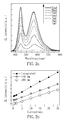
- Figure 2a is an electroluminescence (EL) spectra of InGaN/GaN nanorod-array white LED at injection currents from 1 mA to 25 mA according to the preferred embodiment of the present invention.
- Two major peaks can be clearly identified at 448 nm (blue-band) and 569 nm (yellow-band) at 20 mA.
- the spectral blue shift with increasing current is negligibly small from 5 mA to 25 mA. This behavior illustrates that the QCSE is insignificant in InGaN nanodisk emitters. While full-color emissions are observed in the micro-EL image ( Fig.
- the efficiency droop phenomenon of InGaN LEDs at high injection current densities is considered the major obstacle hindering high-brightness LEDs for general illumination applications.
- the embodiment of the present invention provides the thick and strain-free InGaN/GaN nanorod heterostructures that can overcome the efficiency droop phenomenon.
- Figure 2b shows plots of EL intensity of integrated LED and EL intensity at two specific wavelengths of two major peaks in Fig. 2a as functions of injection current. Both the blue-and yellow-band intensities increase monotonically with increasing injection current at a constant slope, resulting in drive-current-insensitive white light emission. In addition, the integrated EL shows no sign of intensity degradation.
- Another embodiment provides a single-nanorod LED and its electrical and optical characterization.
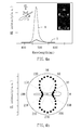
- Figure 3a is I-V curve of a single InGaN/GaN nanorod LED at room temperature according to an embodiment of the present invention. No leakage current can be found at -10 V.
- Inset shows the field-emission scanning electron microscopy (FE-SEM) image and schematic diagram of the measured nanorod structure in which the rod length is about 2 ⁇ m.
- the single-nanorod LED includes only one InGaN nanodisk 4 with 90 nm in diameter and 40 nm in thickness. Scale bar indicates 500 nm.
- the measured I-V characteristics show a good diode behavior.
- single-nanorod diode show no signs of leakage currents, which allows for the measurement of actual current density passing through a single InGaN/GaN nanorod.
- Figure 3b show normalized EL spectra of some single InGaN/GaN nanorod LEDS provided by embodiments of the present invention in which each single InGaN/GaN nanorod LED contains single InGaN nanodisk.
- the spectra show that the emissions from single InGaN nanodisks are monochromatic with narrow spectral widths ( ⁇ 25 nm).
- the corresponding optical microscopy images (not shown) of the diffraction-limited light emissions from single InGaN/GaN nanorod LEDs under forward bias current by 500 nA show color of violet, blue, cyan, green, and yellow, respectively.
- Figure 3c shows EL spectra of a single InGaN/GaN nanorod LED emitting at 475 nm with injection currents from 100 nA to 500 nA.
- the single InGaN/GaN nanorod LED is the same diode measured in figure 3a .
- the acquired relations of EL intensity and relative external quantum efficiency (EQE) with respect to the injection current are shown in the inset.
- the relative EQE is estimated by EL intensity divided by the injection current and was measured by using a fixed emission collection geometry under DC injection mode.
- the relative EQE plot shows a trend of monotonic increase with increasing current density. In contrast, for conventional LEDs, this behavior holds only for current densities ⁇ 10 A/cm 2 .
- the maximum current density without showing efficiency degradation can be directly estimated to be 8,000 A/cm 2 .
- This current density is extremely high in comparison with ⁇ 10 A/cm 2 for typical InGaN LEDs and ⁇ 200 A/cm 2 for an InGaN LED with a thick InGaN active layer.
- This high current density in single-nanorod LEDs without efficiency degradation is made possible by the thick (40 nm) and strain-free nanodisk structure employed in the present invention.
- the measured polarization ratio is -0.85.
- the insets of Fig. 4a show the corresponding optical microscopy images under a 100 ⁇ objective.
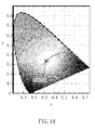
- Figure 4b shows the measured polar plot of linearly polarized EL intensity as a function of the emission polarization with respect to the nanorod long axis.
- a measured polarization ratio of -0.85 represents a high degree of EL polarization, as evidenced in Fig. 4b .
- the observed EL anisotropy is oriented perpendicular to the nanorod axis (a negative ⁇ value).
- a previous study has identified that the optical confinement effect in single GaN nanorods ( ⁇ 100 nm in width) is the cause of polarized luminescence. In this mechanism, the polarization ratio is a function of emission wavelength and nanorod diameter.
- experiments of the present invention show that the polarized luminescence with negative ⁇ is from the InGaN nanodisk structure embedded in the GaN nanorod. Additionally, the measured negative values of ⁇ show weak dependences on the emission wavelength or diameter of the InGaN nanodisks. This behavior is very favorable for future applications requiring polarized light emission.
- the present invention demonstrates that the LED device structure based on thick and strain-free InGaN nanodisk emitters embedded in the self-assembled GaN nanorods can overcome the existing white LED technology limitations, such as the green-yellow gap and the efficiency degradation phenomenon under high-power operation. These devices do not require special nanofabrication techniques and have excellent scaling capability on Si substrates. In addition, the high flexibility in designing InGaN nanodisk emitter structures allows further device optimization for novel lighting and display applications.
- the InGaN/GaN nanorod array samples were grown on 3-inch, P-doped n -type Si(111) (resistivity: 0.001-0.005 ⁇ cm) wafers by nitrogen-plasma-assisted molecular beam epitaxy (PAMBE) under nitrogen-rich conditions, in comparison to the group-III/nitrogen flux ratio used for III-nitride film growth.
- PAMBE nitrogen-plasma-assisted molecular beam epitaxy
- the custom-made PAMBE system DCA Instruments, DCA-600
- ADDON radio-frequency nitrogen plasma source
- the nitrogen plasma source during the growth procedure was at a nitrogen gas flow rate of 3 sccm (standard cubic centimeter per minute) under 500 W RF forward power.
- the in-situ reflection high energy electron diffraction (RHEED) observation confirms that the PAMBE-grown nanorods are wurtzite-type single crystals (the nanorod axial growth direction is along the wurtzite c -axis).
- the in-plane crystallographic axes of the nanorods are found to be the following epitaxial relation: ⁇ 2 11 0> ⁇ [ 1 10] Si ; ⁇ 1 1 00> ⁇ [11 2 ] Si .
- Si-doped n -type GaN nanorod array ( ⁇ 1 ⁇ m in height) was grown first on the Si(111) substrate at 770 °C (growth temperature) [Ga beam equivalent pressure (BEP Ga ): 9 ⁇ 10 -8 Torr]. Subsequently, InGaN nanodisks were grown on top of the n -type GaN nanorods. The emission wavelengths of InGaN nanodisks were controlled by the growth temperature ( T ) and group-III beam fluxes.
- T growth temperature
- group-III beam fluxes group-III beam fluxes.
- three nanodisk growth temperature are T 1 > T 2 > T 3 ( T 1 : 705 °C, T 2 : 700 °C, T 3 : 690 °C).
- T 1 705 °C
- T 2 700 °C
- T 3 690 °C
- three T 1 nanodisks BEP Ga : 7.5 ⁇ 10 -8 Torr; BEP In : 2.6 ⁇ 10 -8 Torr; thickness of InGaN/GaN: ⁇ 25 nm/25 nm), one T 2 nanodisk (BEP Ga : 6.2 ⁇ 10 -8 Torr; BEP In : 3.3 ⁇ 10 -8 Torr; thickness of InGaN/GaN: ⁇ 10 nm/25 nm), and one T 3 nanodisk (BEP Ga : 5.7 ⁇ 10 -8 Torr; BEP In : 3.7 ⁇ 10 -8 Torr; thickness of InGaN/GaN ⁇ 15 nm/25 nm)
- each InGaN nanodisk ranges from 10 to 25 nm, and the GaN barrier thickness is fixed at 25 nm, as shown schematically in Fig. 1a .
- Mg-doped p -type GaN nanorods ( ⁇ 1 ⁇ m in height) were grown at 690 °C. The Ga/N flux ratio was then gradually increased to induce lateral growth of p -type GaN nanorods, thereby forming a quasi-continuous p -type GaN top film.
- White LED devices were fabricated first by dry etching technique (inductively coupled plasma, ICP) to form mesas of 260 ⁇ 280 ⁇ m 2 in size (effective current passing area: ⁇ 47,100 ⁇ m 2 ).
- ICP inductively coupled plasma
- the exposed GaN nanorod part was etched into the Si substrate using a SiO 2 etch mask.
- Contact metals were then evaporated in a 10 -7 Torr vacuum.
- the ohmic contact to n -type Si (111) and p -type GaN layers are Ti/Au (60 nm/40 nm) and Ni/Au (15 nm/35 nm).
- the Ni/Au top contact was thin enough to be transparent for the emitted light.
- the electrodes may be made of other materials, such as indium tin oxide (ITO) or other materials known in the art.
- the InGaN/GaN single-nanorod LED structure used in the present invention was grown on a 3-inch, n -type Si (111) wafer by PAMBE.
- 1.2 ⁇ m, n -type GaN nanorods were grown at 770 °C, and then 40-nm-thick InGaN nanodisks were grown on top of the n -type GaN nanorods_(BEP Ga :3.5 ⁇ 10 -8 Torr; BEP In : 2.6 ⁇ 10 -8 Torr) at 705 °C.
- 800 nm, p -type GaN nanorods were grown on top of the InGaN nanodisks at 685 °C.
- this sample was dipped in 1% hydrogen fluoride (HF) solution for 30 seconds to remove native oxide covered on the nanorods. Then the samples were suspended in isopropanol solution with sonic bath and later were dispersed onto an oxidized ( ⁇ 500-nm-oxide covered) silicon substrate.
- the electrodes were patterned by a standard photolithography and lift off process. Both of the ohmic contacts to n -type and p -type electrodes are Ti/Au (20 nm/35 nm). Contact metals were electron-beam evaporated in a vacuum chamber and the base pressure was in the 10 -7 Torr range. After the contact evaporation process, the LED devices were thermal annealled at 600 °C for 20 seconds in a vacuum chamber with the base pressure in the 10 -9 Torr range.
- HF hydrogen fluoride
- the LED structure shown in Fig. 1a is a horizontal type of LED structure for illustrative purpose, it can be other types, such as a vertical type.
- other substrates may be employed instead of the silicon substrate.
- contact electrodes may be made of other materials or composite materials and may have other configurations and positions.
- the LED structure may be transferred to another substrate, such as a metal substrate, a plastic substrate, a printed circuit board, a transparent substrate, or other substrates for various purposes.
- the substrate may be p-type doped and the position of p-type and n-type GaN nanorod array 3/5 may be interchanged.
- the terms "GaN" and "InGaN” used in this specification may refer to "GaN-based” and "InGaN-based”; the elements of which may be slightly varied or modified. For instance, InGaN may be replaced by AlInGaN and GaN may be replaced by AlGaN, etc.
- other III-nitride single semiconductor alloy systems may replace the GaN/InGaN single semiconductor alloy system used in this embodiment.
- Fig. 5a illustrates a vertical type of LED structure according to another embodiment of this invention.
- the light-emitting diode structure primarily includes a substrate 1, a first electrode 2, a first doped nanorod array 3, a plurality of active light-emitting regions 4, a second doped nanorod array 5, and a second electrode 6.
- the substrate 1 is an n-type doped silicon substrate;
- the first electrode 2 is a composite, multi-layered electrode, e.g., a Ti/Au electrode;
- the first doped nanorod array 3 is an n-type gallium nitride (GaN) nanorod array; each active light-emitting region includes one or more indium gallium nitride (InGaN) nanodisks 4;
- the second doped nanorod array 5 is an p-type gallium nitride (GaN) nanorod array;
- the second electrode 6 is a transparent electrode, e.g., an indium tin oxide (ITO) electrode.
- ITO indium tin oxide
- the first electrode 2 and the first doped nanorod array 3 are disposed on two opposite surfaces of the substrate 1.
- the first doped nanorod array 3 consists of n-type GaN nanorods ohmic contacting with the first electrode 2 through the substrate 1.
- the one or more indium gallium nitride (InGaN) nanodisks 4 are disposed on each of the n-type GaN nanorod 3.
- the p-type GaN nanorod array 5 consists of p-type GaN nanorods disposed on top of the InGaN nanodisks 4 where one p-type GaN nanorod corresponds to one n-type GaN nanorod.
- the second electrode 6, e.g., the ITO electrode 6 is disposed on and ohmic contacts with the p-type GaN nanorod array 5.
- the second electrode 6 is patterned and transparent or sufficient thin to be transparent.
- each of the p-type GaN nanorods 5 and/or each of the n-type GaN nanorods 3 has two ends in which the end near to the transparent electrode 6, i.e., the first end from the transparent electrode 6, may be wider than the other, as shown in Fig. 5b . This structure is helpful to prevent formation of leakage current channels.
- the first electrode 1 may also be patterned so as to control the emitting area if necessary. Notice that the term "and/or" used in this specification refers to "and” or "or.”
- the emitting wavelength i.e., the emitting color or the desired mixing effect of the LED structure
- the number and the emission wavelength of the nanodisk emitters which is controlled by the growth temperature T and flux ratio of elements, e.g., In/Ga beam flux ratio in the epitaxial process for growing the nanodisks.
- the emitting color could be full color over all full-visible-spectrum.
- the light-emitting diode contains three T1 InGaN nanodisks, one T2 InGaN nanodisk, and one T3 InGaN nanodisk, and the growth temperatures for T1, T2, and T3 are T 1 > T 2 > T 3 .
- a GaN barrier layer 7 is interposed between each two of the InGaN nanodisks 4. A white-light emission can be achieved by the above-mentioned structure.
- each nanodisk may range from 10 nm to 25 nm but it may smaller or greater than this range.
- modifications, alternatives, equivalents, and variations for the embodiment of Fig. 5a and Fig. 5b are at least the same as the prior embodiment shown in Fig. 1a .
- Fig. 6a to Fig. 6f illustrate a method to fabricate a vertical type of LED structure as shown in Fig. 5a .
- the substrate 1 may include, but is not limited to, a silicon substrate, a silicon carbide (SiC) substrate, or other semiconductor substrates or other substrates made of other conducting materials.
- a heavy doped n-type silicon (111) substrate 1 with resistivity 0.001-0.005 ⁇ cm is used.
- the substrate 1 may be cleaned by a normal procedure as known in the art.
- the substrate 1 may be dipped into a buffered oxide etching (BOE) solution, such as a hydrofluoric acid (HF) or ammonium fluoride (NH4F) aqueous solution, for removing native oxide layer on the surface of the substrate 1.
- BOE buffered oxide etching
- a first electrode 2 such as a Ti/Au electrode 2 is formed on the bottom surface of the substrate 1 by an evaporation method, such as thermal evaporation, electron-beam evaporation, sputtering, or other methods known in the art.
- an evaporation method such as thermal evaporation, electron-beam evaporation, sputtering, or other methods known in the art.
- an electroluminescent (EL) structure at least including a first doped nanorod array 3, active light-emitting regions 4, and a second doped nanorod array 5 is formed by an epitaxial process, preferably the mentioned nitrogen-plasma-assisted molecular beam epitaxy (PAMBE).
- the first doped nanorod array 3 is an n-type gallium nitride (GaN) nanorod array; each active light-emitting region 4 includes one or more indium gallium nitride (InGaN) nanodisks; and the second doped nanorod array 5 is an p-type gallium nitride (GaN) nanorod array.
- the following illustrates a particular example to grow the electroluminescent (EL) structure.
- the PAMBE process is performed under nitrogen-rich conditions, in comparison to the group-III/nitrogen flux ratio used for III-nitride film growth.
- the nitrogen plasma source during the growth procedure is at a nitrogen gas flow rate of 3 sccm (standard cubic centimeter per minute) under 500 W RF forward power.
- the in-situ reflection high energy electron diffraction (RHEED) observation confirms that the grown nanorods are wurtzite-type single crystals, i.e., the nanorod axial growth direction is along the wurtzite c-axis.
- the in-plane crystallographic axes of the nanorods are found to be the following epitaxial relation: ⁇ 2 11 10> ⁇ [ 1 10] Si ; ⁇ 1 1 00> ⁇ [11 2 ] Si .
- Si-doped n -type GaN nanorod array with about 1 ⁇ m in height is grown first on the Si(111) substrate at a growth temperature 770 °C and a Ga beam equivalent pressure (BEP Ga ) 9 ⁇ 10 -8 Torr. Subsequently, InGaN nanodisks are grown on top of the n -type GaN nanorods.
- the emission wavelengths of InGaN nanodisks are controlled by the growth temperature ( T ) and group-III beam fluxes.
- T growth temperature
- group-III beam fluxes three nanodisk growth temperature are T 1 > T 2 > T 3 ( T 1 : 705 °C, T 2 : 700 °C, T 3 : 690 °C).
- This structure is used for fabricating white LEDs and the growing conditions are: three T 1 nanodisks (BEP Ga : 7.5 ⁇ 10 -8 Torr; BEP In : 2.6 ⁇ 10 -8 Torr; thickness of InGaN/GaN: ⁇ 25 nm/25 nm), one T 2 nanodisk (BEP Ga : 6 .
- each InGaN nanodisk may range from 10 nm to 25 nm and the GaN barrier thickness may be fixed at 25 nm, as shown schematically in Fig. 5a and Fig. 5b .
- Mg-doped p -type GaN nanorods with height about 1 ⁇ m are grown at 690 °C.
- the Ga/N flux ratio may be gradually increased to induce lateral growth of n -type GaN nanorods and/or p -type GaN nanorods, thereby forming a quasi-continuous p -type GaN top film.
- other III-nitride single semiconductor alloy systems may replace the GaN/InGaN single semiconductor alloy system used in this embodiment.
- a spin on glass (SOG) process may be performed to fill gaps between the nanorods.
- a liquid dielectric material or a oxide-based material may be used for this purpose.
- a patterned photoresist layer 8 with defined aperture 8a is formed on the second doped nanorod array 5.
- This step can be performed by methods known in the art, such as photolithography or E-beam lithography.
- a photoresist layer is first coated on the second doped nanorod array 5, and then a pattern is transferred to the photoresist layer by illuminating with suitable light source, and thus apertures 8a is defined.
- other mask materials such as anodic aluminum oxide (AAO) substrate, may replace the photoresist layer 8 for patterning.
- AAO anodic aluminum oxide
- a second electrode 6 is then formed on the second doped nanorod array 5 within the aperture 8a by the mentioned evaporation method.
- another photoresist layer (not shown) may be formed on the second electrode 6, so as to remove unused nanorod array by a proper method, such as an etching method, preferably the inductively coupled plasma (ICP) etching method. Notice that this step may be omitted for saving cost.
- a proper method such as an etching method, preferably the inductively coupled plasma (ICP) etching method. Notice that this step may be omitted for saving cost.
- ICP inductively coupled plasma
- a mask may be used to define where the electroluminescent structure 3/4/5/7 is grown, so that the step of Fig. 6f can be omitted.
- the first electrode 2 may be formed after the electroluminescent structure 3/4/5/7 is formed.
- Fig. 7a is a simplified diagram illustrating a light-emitting diode (LED) display according to a preferred embodiment of this invention.
- the light-emitting diode display primarily includes a plurality of pixels 9, and each pixel 9 comprises one or more first light-emitting diodes, e.g. "B", one or more second light-emitting diodes e.g. "G”, and one or more third light-emitting diodes e.g. "R”, in which the first, the second, and the third light-emitting diodes B/G/R respectively emit a first, a second, and a third color, which are preferably blue, green, and red.
- each pixel 9 includes about 100 red, 100 green, and 100 blue light-emitting diodes B/G/R in this embodiment.
- the pixels 9 are arranged or directly formed on a substrate 1.
- the substrate 1 may be a conductive substrate or a non-conductive substrate coated with a conductive surface or pattern on the top surface of the substrate 1.
- the substrate 1 may be made of a material selected from a group consisted essentially of silicon, silicon carbide, semiconductor, plastic material, metal, glass, and combinations thereof.
- Each of the blue, green, and red light-emitting diodes B/G/R comprise a first doped nanorod 3, an active light-emitting region 4/4'/4" arranged on the first doped nanorod 3, a second doped nanorod 5 arranged on the active light-emitting region 4/4'/4", and a second electrode 6 arranged on the second doped nanorod 5.
- a first electrode 2 is preferably arranged on the bottom surface of the substrate 1 for ohmic contact with the first doped nanorods 3 of all the LED diodes R/G/B via the substrate 1.
- the first electrode 2 is integrated in this embodiment, but in other embodiments, it may be plural and each corresponds to one first doped nanorod 3.
- the first electrode 2 is made to be plural and are formed on the top surface for respective ohmic contact with the first doped nanorods 3 via the substrate 1.
- the substrate 1 is a heavily n-doped silicon substrate.
- the first electrode 2 is a composite, multi-layered electrode, e.g., a Ti/Au electrode.
- the first doped nanorod 3 is an n-type gallium nitride (GaN) nanorod.
- the active light-emitting region 4/4'/4" includes one or more indium gallium nitride (InGaN) nanodisks, e.g., one T1 nanodisk for blue emission, one T2 nanodisk for green emission, and one T3 nanodisk for red emission.
- InGaN indium gallium nitride
- the second doped nanorod 5 is a p-type gallium nitride (GaN) nanorod.
- the second electrode 6 is a transparent electrode, e.g., an indium tin oxide (ITO) electrode.
- a GaN barrier layer 7 may be disposed between each nanodisk T1/T2/T3 and the p-type GaN nanorod 5 and between the nanodisks T1/T2/T3 for two or more nanodisks T1/T2/T3. Notice that the number of the nanodisks T1/T2/T3 may be multiple for adjusting the emission wavelength of the LED diodes, and the nanodisks T1/T2/T3 may be made of same material, e.g., InGaN, but with different thicknesses.
- the second electrode 6 is transparent or sufficient thin to be transparent.
- the nanodisks T1/T2/T3 are grown at different temperature; in this embodiment, T1 nanodisks have the highest growing temperature, T2 the second, and T3 the third.
- the order to grow the nanodisks is from the highest growing temperature to the lowest growing temperature, i.e., T1, T2, and then T3. If the nanodisks are grown in the reverse order, i.e., T3, T2, and then T1, the content of indium may be unstable and thus alters the emission wavelengths of the nanodisks.
- Fig. 7b showing a modified LED display of Fig. 7a , in which the p-type GaN nanorod 5 and/or the n-type GaN nanorod 3 has two ends in which the end near the second electrode 6, i.e., the first end from the second electrode 6, is wider than the other. This structure is helpful to prevent current overflow and/or prevent formation of leakage current channels.
- each pixel 9 may further comprise one or more fourth light-emitting diodes for emitting a fourth color, one or more fifth light-emitting diodes for emitting a fifth color, and so on.
- the fourth color may be, but is not limited to, yellow gold.
- the substrate 1 may be sliced to form a plurality of single packages and each comprises one or more pixels 9, and the packages are then mounted on another substrate, e.g., a printed circuit board or a flexible printed circuit board.
- Other modifications, alternatives, and variations may be similar to those mentioned in the forgoing embodiments.
- Fig. 8a to Fig. 8j are simplified diagrams illustrating a method of this invention to fabricate a LED display as shown in Fig. 7a .
- the substrate 1 may include, but is not limited to, a silicon substrate, a silicon carbide (SiC) substrate, or other semiconductor substrates or other substrates made of other conducting materials.
- a heavy doped n-type silicon (111) substrate 1 with resistivity 0.001-0.005 ⁇ cm is used.
- the substrate 1 may be cleaned by a normal procedure as known in the art.
- the substrate 1 may be dipped into a buffered oxide etching (BOE) solution, such as a hydrofluoric acid (HF) or ammonium fluoride (NH 4 F) aqueous solution, for removing native oxide layer on the surface of the substrate 1.
- BOE buffered oxide etching
- a plurality of first doped nanorods 3 are formed on the top surface of the substrate 1 by an epitaxial process, preferably the mentioned nitrogen-plasma-assisted molecular beam epitaxy (PAMBE). Notice that the first doped nanorods 3 may be formed on selected area of the substrate 1 by a mask, or formed on essentially whole area of the substrate 1. In this embodiment, the first doped nanorods 3 are n-type gallium nitride (GaN) nanorods.
- GaN gallium nitride
- a first mask 8 with defined apertures 8a is arranged or formed on the first doped nanorods 3, exposing a plurality of first top surfaces 3a of selected first doped nanorods 3.
- the first mask 8 may be a patterned photoresist layer or other mask materials, such as silicon dioxide, anodic aluminum oxide (AAO), and titanium, etc..
- the patterned photoresist layer 8 can be formed by methods known in the art, such as photolithography or electron-beam lithography. For example, a photoresist layer is first coated on the first doped nanorods 3, and then a pattern is transferred to the photoresist layer by exposing to a suitable light source, and thus apertures 8a are defined.
- a plurality of first active light-emitting regions 4 are respectively formed on the first top surfaces 3a of the first doped nanorods 3 by using the epitaxial process mentioned in Fig. 8b .
- Each of the first light-emitting regions 4 comprises one or more nanodisks.
- each first light-emitting region 4 comprises a mentioned T1 nanodisk and a mentioned barrier layer 7 for emitting blue color.
- the first mask 8 is then removed or stripped by an etching (e. g., BOE) solution.
- a second mask 8' with defined apertures 8a' is arranged or formed on the first doped nanorods 3, exposing a plurality of second top surfaces 3b of selected first doped nanorods 3.
- the second mask 8' may be essentially the same as the first mask 8 except the locations of the aperture 8a'.
- a plurality of second active light-emitting regions 4' are respectively formed on the second top surfaces 3b of the first doped nanorods 3 by using the epitaxial process mentioned in Fig. 8b .
- Each second active light-emitting regions 4' comprises one or more nanodisks.
- each second active light-emitting region 4' comprises a mentioned T2 nanodisk and a mentioned barrier layer 7 for emitting green color.
- the second mask 8' is then removed or stripped by the buffered oxide etching (BOE) solution.
- BOE buffered oxide etching
- a third mask 8" with defined apertures 8a" is arranged or formed on the first doped nanorods 3, exposing a plurality of third top surfaces 3c of selected first doped nanorods 3.
- the third mask 8" may be essentially the same as the first mask 8 except the positions of the aperture 8a".
- a plurality of third active light-emitting regions 4" are respectively formed on the third top surfaces 3c of the first doped nanorods 3 by using the epitaxial process mentioned in Fig. 8b .
- Each third active light-emitting regions 4" comprises one or more nanodisks.
- each third active light-emitting region 4" comprises a mentioned T3 nanodisk and a mentioned barrier layer 7 for emitting red color.
- the third mask 8" is then removed or stripped by the buffered oxide etching (BOE) solution.
- BOE buffered oxide etching
- a plurality of second doped nanorods 5 are respectively formed on the top surfaces of the first, second, and third active light-emitting regions 4/4'/4" by using the mentioned epitaxial process.
- the second doped nanorods 5 are p-type gallium nitride (GaN) nanorods.
- a first electrode 2 such as a Ti/Au electrode 2 is formed on the bottom surface of the substrate 1 by an evaporation method, such as thermal evaporation, electron-beam evaporation, sputtering, or other methods known in the art.
- a plurality of second electrodes 6 are formed on the top surfaces of the second doped nanorods 5 by a self-aligned manner.
- the PAMBE process used in this embodiment may have essentially same features as mentioned in the foregoing embodiments.
- the PAMBE process is performed under nitrogen-rich conditions, in comparison to the group-III/nitrogen flux ratio used for III-nitride film growth.
- the nitrogen plasma source during the growth procedure is at a nitrogen gas flow rate of 3 sccm under 500 W RF forward power.
- the grown nanorods are wurtzite-type single crystals, i.e., the nanorod axial growth direction is along the wurtzite c -axis.
- the in-plane crystallographic axes of the nanorods are found to be the following epitaxial relation: ⁇ 2 11 0> ⁇ [ 1 10] Si ; ⁇ 1 1 00> ⁇ [11 2 ] Si .
- the Si-doped n -type GaN nanorods is about have a height about 1 ⁇ m with a growth temperature 770 °C and a Ga beam equivalent pressure (BEP Ga ) 9 ⁇ 10 -8 Torr.
- BEP Ga Ga beam equivalent pressure
- InGaN nanodisks are grown on top of the n -type GaN nanorods.
- the emission wavelengths of InGaN nanodisks are controlled by the growth temperature ( T ) and group-III beam fluxes.
- T growth temperature
- group-III beam fluxes group-III beam fluxes.
- the growth temperature of the nanodisks T 1 / T 2 / T 3 are 705 °C, 700 °C, and 690 °C repestively. and the growing conditions are: T 1 nanodisk (BEP Ga : 7.5 ⁇ 10 -8 Torr; BEP In : 2.6 ⁇ 10 -8 Torr; thickness of InGaN/GaN: ⁇ 25 nm/25 nm), T 2 nanodisk (BEP Ga : 6.2 ⁇ 10 -8 Torr; BEP In : 3.3 ⁇ 10 -8 Torr; thickness of InGaN/GaN: ⁇ 10 nm/25 nm), and T 3 nanodisk (BEP Ga : 5.7 ⁇ 10 -8 Torr; BEP In : 3.7 ⁇ 10 -8 Torr; thickness of InGaN/GaN ⁇ 15 nm/25 nm).
- each InGaN nanodisk may range from 10 nm to 25 nm and the thickness of the GaN barrier 7 is about 25 nm, as shown schematically in Fig. 7a and Fig. 7b .
- Mg-doped p -type GaN nanorods with height about 1 ⁇ m are grown at 690 °C.
- the Ga/N flux ratio may be gradually increased to induce lateral growth of n -type GaN nanorods and/or p -type GaN nanorods, thereby forming a quasi-continuous p -type GaN top film.
- each of the first, second, and third active light-emitting regions is made from a InGaN single semiconductor alloy system.
- each of the first, second, and third active light-emitting regions may be made of other III-nitride single semiconductor alloy systems.
- a spin on glass (SOG) process may be performed to fill gaps between the nanorods within a sub-pixel, i.e., between nanorods for emitting a same color within a pixel.
- SOG spin on glass
- a liquid dielectric material or an oxide-based material may be used for this purpose.
- another mask (not shown) may be formed on the second electrode 6, so as to remove unused nanorods by etching, such as the inductively coupled plasma (ICP) etching method. This step may be omitted for simplicity.
- ICP inductively coupled plasma
- the first electrode 2 may be formed after the light-emitting diodes R/G/B are formed.
- a mask may be used to define where the first, second, and third light-emitting diodes B/G/R are grown, so that the ICP etching is unnecessary.
- additional steps may follow to this method.
- the substrate 1 may be sliced to form a plurality of single packages and each comprises one or more pixels 9, and the packages are then mounted on another substrate, e.g., a printed circuit board or a flexible printed circuit board.
- the first, second, and third light-emitting diodes B/G/R may be transferred to one or more substrates for other purposes.
- the above method illustrates how to fabricate a light-emitting diode display with three primary color, namely red, green, and blue.
- it can be analog to fabricate an LED display with more primary colors, e.g., four primary colors.
- an additional mask with defined apertures is arranged or formed on the first doped nanorods 3 to expose a plurality of fourth top surfaces of selected first doped nanorods, a fourth active light-emitting region is then formed on each of the fourth top surfaces, and a second doped nanorod is formed on each of the fourth active light-emitting region.
- Fig. 9 is a simplified diagram showing a driving method of the LED displays of this invention.
- each pixel 9 comprises three sub-pixels, namely red (R), green (G), and blue (B) sub-pixels, and each sub-pixel comprises one or more LEDs for emitting a same color.
- the first electrode of the sub-pixels R/G/B is a common electrode while the second electrodes of the sub-pixels are separately connected to at least one signal source.
- the signal source separately provides desired voltages to sub-pixels of each pixel, and a color image is displayed according to the combination of emissions from these three types of sub-pixels.
- this invention provides LED displays with simple structure and fabricating method. All light-emitting diodes emitting different wavelengths can be grown on the same substrate, and the growth substrate may be used also as the display substrate.
- the fabrication methods of this invention can omit those complicated steps for transferring the light-emitting diodes and thus provide a more reliable and cost-down approach.
Applications Claiming Priority (1)
| Application Number | Priority Date | Filing Date | Title |
|---|---|---|---|
| US13/471,329 US8835903B2 (en) | 2010-07-29 | 2012-05-14 | Light-emitting diode display and method of producing the same |
Publications (2)
| Publication Number | Publication Date |
|---|---|
| EP2665100A2 true EP2665100A2 (de) | 2013-11-20 |
| EP2665100A3 EP2665100A3 (de) | 2015-01-07 |
Family
ID=48463756
Family Applications (1)
| Application Number | Title | Priority Date | Filing Date |
|---|---|---|---|
| EP13167655.3A Withdrawn EP2665100A3 (de) | 2012-05-14 | 2013-05-14 | Lichtemittierende Diodenanzeige und Verfahren zu deren Herstellung |
Country Status (4)
| Country | Link |
|---|---|
| EP (1) | EP2665100A3 (de) |
| KR (1) | KR101473288B1 (de) |
| CN (1) | CN103426373A (de) |
| TW (1) | TWI541992B (de) |
Cited By (12)
| Publication number | Priority date | Publication date | Assignee | Title |
|---|---|---|---|---|
| FR3023066A1 (fr) * | 2014-06-30 | 2016-01-01 | Aledia | Dispositif optoelectronique comprenant des diodes electroluminescentes et un circuit de commande |
| EP3116036A1 (de) * | 2015-07-07 | 2017-01-11 | Technische Universität Braunschweig | Lichtemittierende vorrichtung, optische detektionsvorrichtung, verfahren zum betreiben und computerprogramm |
| FR3044470A1 (fr) * | 2015-11-30 | 2017-06-02 | Commissariat Energie Atomique | Dispositif optoelectronique comportant des structures semiconductrices tridimensionnelles en configuration axiale |
| WO2017153600A1 (fr) * | 2016-03-11 | 2017-09-14 | Valeo Comfort And Driving Assistance | Écran actif et afficheur tête haute comprenant un tel écran |
| CN108206228A (zh) * | 2016-12-19 | 2018-06-26 | 三星显示有限公司 | 发光设备以及发光设备的制造方法 |
| EP3373344A1 (de) * | 2013-12-19 | 2018-09-12 | Aledia | Optoelektronische vorrichtung mit leuchtdioden mit verbesserter lichtextraktion |
| FR3076080A1 (fr) * | 2017-12-27 | 2019-06-28 | Aledia | Pseudo-substrat pour dispositif optoelectronique et son procede de fabrication |
| WO2019243746A1 (fr) * | 2018-06-20 | 2019-12-26 | Aledia | Dispositif optoelectronique comprenant une matrice de diodes |
| CN113396480A (zh) * | 2018-12-05 | 2021-09-14 | 原子能与替代能源委员会 | 多色电致发光显示装置及其制造方法 |
| US11328415B2 (en) | 2017-06-15 | 2022-05-10 | Fujifilm Corporation | Medical image processing device, endoscope system, and method of operating medical image processing device |
| WO2022241305A1 (en) * | 2021-05-14 | 2022-11-17 | The Regents Of The University Of Michigan | High efficiency ingan light emitting diodes |
| WO2024073095A1 (en) * | 2022-09-30 | 2024-04-04 | The Regents Of The University Of Michigan | An ultrahigh efficiency excitonic device |
Families Citing this family (14)
| Publication number | Priority date | Publication date | Assignee | Title |
|---|---|---|---|---|
| WO2016052987A1 (ko) * | 2014-09-29 | 2016-04-07 | 한국기계연구원 | 플라즈모닉 광흡수체, 이를 포함하는 플라즈모닉 광촉매 기판 및 이의 제조방법 |
| KR101845907B1 (ko) | 2016-02-26 | 2018-04-06 | 피에스아이 주식회사 | 초소형 led 모듈을 포함하는 디스플레이 장치 |
| FR3053437B1 (fr) * | 2016-06-30 | 2019-06-28 | Valeo Vision | Dispositif d'eclairage et/ou de signalisation ameliore, notamment pour vehicule automobile |
| TWI613775B (zh) * | 2016-08-24 | 2018-02-01 | 國立清華大學 | 降低電流路徑熱應力之晶片 |
| TWI718343B (zh) * | 2016-10-24 | 2021-02-11 | 瑞典商Glo公司 | 發光二極體、顯示裝置及直視顯示裝置 |
| FR3064109A1 (fr) * | 2017-03-20 | 2018-09-21 | Commissariat A L'energie Atomique Et Aux Energies Alternatives | Structure a nanofils et procede de realisation d'une telle structure |
| TWI676285B (zh) * | 2017-05-04 | 2019-11-01 | 國立交通大學 | 無電極遮光之發光二極體顯示器的結構及其製程 |
| US10263151B2 (en) * | 2017-08-18 | 2019-04-16 | Globalfoundries Inc. | Light emitting diodes |
| CN110504338A (zh) * | 2018-05-18 | 2019-11-26 | 睿明科技股份有限公司 | 微元件工艺及制作显示器面板的方法 |
| CN110556453B (zh) * | 2018-05-30 | 2020-11-06 | 中国科学院苏州纳米技术与纳米仿生研究所 | 有序Si基Al1-xGaxN量子点的可控外延生长方法 |
| CN110690246B (zh) * | 2019-10-16 | 2022-03-25 | 福州大学 | 一种非直接电学接触取向有序nLED发光显示器件 |
| KR20230004770A (ko) * | 2020-07-21 | 2023-01-06 | 엘지전자 주식회사 | 디스플레이 장치의 제조에 사용되는 전사 기판, 디스플레이 장치 및 디스플레이 장치의 제조 방법 |
| KR102542483B1 (ko) * | 2020-12-31 | 2023-06-12 | 국민대학교산학협력단 | 초박형 led 소자, 이를 포함하는 잉크젯용 잉크 및 광원 |
| KR102573265B1 (ko) * | 2021-03-25 | 2023-08-31 | 국민대학교산학협력단 | 초박형 led 전극어셈블리 및 이의 제조방법 |
Family Cites Families (6)
| Publication number | Priority date | Publication date | Assignee | Title |
|---|---|---|---|---|
| JP2003158296A (ja) * | 2001-11-22 | 2003-05-30 | Sharp Corp | 窒化物半導体発光デバイスチップとその製造方法 |
| GB2437110B (en) * | 2006-04-12 | 2009-01-28 | Cambridge Display Tech Ltd | Optoelectronic display and method of manufacturing the same |
| US7687812B2 (en) * | 2007-06-15 | 2010-03-30 | Tpo Displays Corp. | Light-emitting diode arrays and methods of manufacture |
| JP2009129941A (ja) * | 2007-11-20 | 2009-06-11 | Panasonic Corp | 発光デバイス |
| WO2010014032A1 (en) * | 2008-07-07 | 2010-02-04 | Glo Ab | A nanostructured LED |
| US8669128B2 (en) * | 2010-07-29 | 2014-03-11 | National Tsing Hua University | Method of producing III-nitride light-emitting diode |
-
2013
- 2013-05-14 TW TW102117123A patent/TWI541992B/zh active
- 2013-05-14 EP EP13167655.3A patent/EP2665100A3/de not_active Withdrawn
- 2013-05-14 CN CN2013101778720A patent/CN103426373A/zh active Pending
- 2013-05-14 KR KR1020130054286A patent/KR101473288B1/ko active IP Right Grant
Non-Patent Citations (1)
| Title |
|---|
| CHEN, H.-Y.; LIN, H.-W.; SHEN, C.-H.; GWO, S.: "Structure and photoluminescence properties of epitaxially oriented GaN nanorods grown on Si(111) by plasma-assisted molecular-beam epitaxy", APPL. PHYS. LETT., vol. 89, 2006, pages 243105, XP012087647, DOI: doi:10.1063/1.2404597 |
Cited By (35)
| Publication number | Priority date | Publication date | Assignee | Title |
|---|---|---|---|---|
| EP3373344A1 (de) * | 2013-12-19 | 2018-09-12 | Aledia | Optoelektronische vorrichtung mit leuchtdioden mit verbesserter lichtextraktion |
| FR3023066A1 (fr) * | 2014-06-30 | 2016-01-01 | Aledia | Dispositif optoelectronique comprenant des diodes electroluminescentes et un circuit de commande |
| WO2016001200A1 (fr) * | 2014-06-30 | 2016-01-07 | Aledia | Dispositif optoelectronique comprenant des diodes electroluminescentes et un circuit de commande |
| EP3410482A1 (de) * | 2014-06-30 | 2018-12-05 | Aledia | Optoelektronische vorrichtung, die elektrolumineszenzdioden auf einen steuerschaltkreis umfasst |
| US10304812B2 (en) | 2014-06-30 | 2019-05-28 | Aledia | Optoelectronic device including light-emitting diodes and a control circuit |
| EP3116036A1 (de) * | 2015-07-07 | 2017-01-11 | Technische Universität Braunschweig | Lichtemittierende vorrichtung, optische detektionsvorrichtung, verfahren zum betreiben und computerprogramm |
| US10201054B2 (en) | 2015-07-07 | 2019-02-05 | Technische Universitaet Braunschweig | Optical detection device, its method for operating and computer program |
| US10403787B2 (en) | 2015-11-30 | 2019-09-03 | Commissariat A L'energie Atomique Et Aux Energies Alternatives | Optoelectronic device comprising three-dimensional semiconductor structures in an axial configuration |
| EP3384537B1 (de) * | 2015-11-30 | 2019-10-30 | Commissariat à l'Energie Atomique et aux Energies Alternatives | Optoelektronische vorrichtung mit tridimensionalen halbleiterstrukturen in axialer konfiguration |
| KR20180112764A (ko) * | 2015-11-30 | 2018-10-12 | 꼼미사리아 아 레네르지 아토미끄 에뜨 옥스 에너지스 앨터네이티브즈 | 축방향 구성의 3차원 반도체 구조를 포함하는 광전자 소자 |
| WO2017093646A1 (fr) * | 2015-11-30 | 2017-06-08 | Commissariat à l'énergie atomique et aux énergies alternatives | Dispositif optoelectronique comportant des structures semiconductrices tridimensionnelles en configuration axiale |
| JP2019502257A (ja) * | 2015-11-30 | 2019-01-24 | コミサリア ア レネルジ アトミク エ オウ エネルジ アルタナティヴ | 軸方向配置の3次元半導体構造を有する光電子素子 |
| FR3044470A1 (fr) * | 2015-11-30 | 2017-06-02 | Commissariat Energie Atomique | Dispositif optoelectronique comportant des structures semiconductrices tridimensionnelles en configuration axiale |
| WO2017153600A1 (fr) * | 2016-03-11 | 2017-09-14 | Valeo Comfort And Driving Assistance | Écran actif et afficheur tête haute comprenant un tel écran |
| CN109791927A (zh) * | 2016-03-11 | 2019-05-21 | 法雷奥舒适驾驶助手公司 | 屏和包括这种屏的平视显示器 |
| CN109791927B (zh) * | 2016-03-11 | 2023-10-20 | 法雷奥舒适驾驶助手公司 | 屏和包括这种屏的平视显示器 |
| FR3048817A1 (fr) * | 2016-03-11 | 2017-09-15 | Valeo Comfort & Driving Assistance | Ecran et afficheur tete haute comprenant un tel ecran |
| US11275238B2 (en) | 2016-03-11 | 2022-03-15 | Valeo Comfort And Driving Assistance | Active screen and head-up display comprising such a screen |
| CN108206228A (zh) * | 2016-12-19 | 2018-06-26 | 三星显示有限公司 | 发光设备以及发光设备的制造方法 |
| US11610934B2 (en) | 2016-12-19 | 2023-03-21 | Samsung Display Co., Ltd. | Light emitting device and manufacturing method of the light emitting device |
| CN108206228B (zh) * | 2016-12-19 | 2022-11-25 | 三星显示有限公司 | 发光设备以及发光设备的制造方法 |
| US11328415B2 (en) | 2017-06-15 | 2022-05-10 | Fujifilm Corporation | Medical image processing device, endoscope system, and method of operating medical image processing device |
| WO2019129945A1 (fr) * | 2017-12-27 | 2019-07-04 | Aledia | Pseudo-substrat pour dispositif optoélectronique et son procédé de fabrication |
| US10937827B2 (en) | 2017-12-27 | 2021-03-02 | Aledia | Pseudo-substrate for optoelectronic device and its manufacturing method |
| CN111527607B (zh) * | 2017-12-27 | 2022-01-18 | 艾利迪公司 | 用于光电装置的伪衬底及其制造方法 |
| KR20200096661A (ko) * | 2017-12-27 | 2020-08-12 | 알레디아 | 광전자 디바이스용 의사-기판 및 그 제조 방법 |
| CN111527607A (zh) * | 2017-12-27 | 2020-08-11 | 艾利迪公司 | 用于光电装置的伪衬底及其制造方法 |
| FR3076080A1 (fr) * | 2017-12-27 | 2019-06-28 | Aledia | Pseudo-substrat pour dispositif optoelectronique et son procede de fabrication |
| FR3083002A1 (fr) * | 2018-06-20 | 2019-12-27 | Aledia | Dispositif optoelectronique comprenant une matrice de diodes |
| WO2019243746A1 (fr) * | 2018-06-20 | 2019-12-26 | Aledia | Dispositif optoelectronique comprenant une matrice de diodes |
| EP4235822A3 (de) * | 2018-06-20 | 2023-09-20 | Aledia | Optoelektronische vorrichtung mit einer diodenmatrix |
| CN113396480A (zh) * | 2018-12-05 | 2021-09-14 | 原子能与替代能源委员会 | 多色电致发光显示装置及其制造方法 |
| CN113396480B (zh) * | 2018-12-05 | 2024-03-26 | 原子能与替代能源委员会 | 多色电致发光显示装置及其制造方法 |
| WO2022241305A1 (en) * | 2021-05-14 | 2022-11-17 | The Regents Of The University Of Michigan | High efficiency ingan light emitting diodes |
| WO2024073095A1 (en) * | 2022-09-30 | 2024-04-04 | The Regents Of The University Of Michigan | An ultrahigh efficiency excitonic device |
Also Published As
| Publication number | Publication date |
|---|---|
| CN103426373A (zh) | 2013-12-04 |
| KR101473288B1 (ko) | 2014-12-16 |
| KR20130127389A (ko) | 2013-11-22 |
| EP2665100A3 (de) | 2015-01-07 |
| TWI541992B (zh) | 2016-07-11 |
| TW201347164A (zh) | 2013-11-16 |
Similar Documents
| Publication | Publication Date | Title |
|---|---|---|
| US8835903B2 (en) | Light-emitting diode display and method of producing the same | |
| EP2665100A2 (de) | Lichtemittierende Diodenanzeige und Verfahren zu deren Herstellung | |
| US8242523B2 (en) | III-Nitride light-emitting diode and method of producing the same | |
| JP2007123731A (ja) | 半導体発光素子および半導体発光装置 | |
| CN113646894A (zh) | 纳米线发光开关装置及其方法 | |
| US7572653B2 (en) | Method of fabricating light emitting diode | |
| US8669128B2 (en) | Method of producing III-nitride light-emitting diode | |
| KR101666836B1 (ko) | 형광체 없는 백색 발광다이오드 성장 기술 | |
| Hartensveld | InGaN color tunable full color passive matrix | |
| KR20140025045A (ko) | 광 추출 향상 기술이 반영된 질화물 반도체 에피 구조의 기판 및 템플레이트 제조 방법 | |
| KR20200035336A (ko) | Uv-led 및 디스플레이 | |
| US20220262848A1 (en) | Led arrays | |
| US7888152B2 (en) | Method of forming laterally distributed LEDs | |
| KR20080030042A (ko) | 질화물 다층 양자 웰을 가지는 나노막대 어레이 구조의발광 다이오드 | |
| KR102110446B1 (ko) | 나노와이어 백색 발광소자 및 그 제조 방법 | |
| Kovác et al. | Advanced light emitting devices for optoelectronic applications | |
| EP3644379B1 (de) | Uv-led und anzeige | |
| US20160218246A1 (en) | EPITAXIAL TRANSPARENT CONDUCTIVE OXIDE ELECTRODES FOR GaN LEDS | |
| KR101148758B1 (ko) | 발광다이오드 및 이의 제조방법 | |
| US20230317764A1 (en) | Display device and method of fabricating the same | |
| US20240145629A1 (en) | Structured epitaxy for light emitting diode array | |
| TWI497764B (zh) | Iii族-氮化物發光二極體與其形成方法 | |
| JP2001223386A (ja) | 窒化物半導体素子 | |
| TW202236699A (zh) | 發光元件、發光元件的製造方法及包含發光元件的顯示裝置 | |
| KR100801618B1 (ko) | 발광 소자 및 그 제조방법 |
Legal Events
| Date | Code | Title | Description |
|---|---|---|---|
| PUAI | Public reference made under article 153(3) epc to a published international application that has entered the european phase |
Free format text: ORIGINAL CODE: 0009012 |
|
| AK | Designated contracting states |
Kind code of ref document: A2 Designated state(s): AL AT BE BG CH CY CZ DE DK EE ES FI FR GB GR HR HU IE IS IT LI LT LU LV MC MK MT NL NO PL PT RO RS SE SI SK SM TR |
|
| AX | Request for extension of the european patent |
Extension state: BA ME |
|
| PUAL | Search report despatched |
Free format text: ORIGINAL CODE: 0009013 |
|
| AK | Designated contracting states |
Kind code of ref document: A3 Designated state(s): AL AT BE BG CH CY CZ DE DK EE ES FI FR GB GR HR HU IE IS IT LI LT LU LV MC MK MT NL NO PL PT RO RS SE SI SK SM TR |
|
| AX | Request for extension of the european patent |
Extension state: BA ME |
|
| RIC1 | Information provided on ipc code assigned before grant |
Ipc: H01L 33/08 20100101ALI20141201BHEP Ipc: H01L 33/06 20100101ALN20141201BHEP Ipc: H01L 33/18 20100101ALN20141201BHEP Ipc: H01L 33/32 20100101ALN20141201BHEP Ipc: H01L 27/15 20060101AFI20141201BHEP |
|
| 17P | Request for examination filed |
Effective date: 20150618 |
|
| RBV | Designated contracting states (corrected) |
Designated state(s): AL AT BE BG CH CY CZ DE DK EE ES FI FR GB GR HR HU IE IS IT LI LT LU LV MC MK MT NL NO PL PT RO RS SE SI SK SM TR |
|
| STAA | Information on the status of an ep patent application or granted ep patent |
Free format text: STATUS: EXAMINATION IS IN PROGRESS |
|
| 17Q | First examination report despatched |
Effective date: 20180523 |
|
| STAA | Information on the status of an ep patent application or granted ep patent |
Free format text: STATUS: THE APPLICATION IS DEEMED TO BE WITHDRAWN |
|
| 18D | Application deemed to be withdrawn |
Effective date: 20181003 |