EP2662902A1 - Solarzellenmodul und Herstellungsverfahren davon - Google Patents
Solarzellenmodul und Herstellungsverfahren davon Download PDFInfo
- Publication number
- EP2662902A1 EP2662902A1 EP13166633.1A EP13166633A EP2662902A1 EP 2662902 A1 EP2662902 A1 EP 2662902A1 EP 13166633 A EP13166633 A EP 13166633A EP 2662902 A1 EP2662902 A1 EP 2662902A1
- Authority
- EP
- European Patent Office
- Prior art keywords
- solar cell
- carbon nanotubes
- interconnector
- cell devices
- cell module
- Prior art date
- Legal status (The legal status is an assumption and is not a legal conclusion. Google has not performed a legal analysis and makes no representation as to the accuracy of the status listed.)
- Withdrawn
Links
Images



Classifications
-
- H—ELECTRICITY
- H10—SEMICONDUCTOR DEVICES; ELECTRIC SOLID-STATE DEVICES NOT OTHERWISE PROVIDED FOR
- H10F—INORGANIC SEMICONDUCTOR DEVICES SENSITIVE TO INFRARED RADIATION, LIGHT, ELECTROMAGNETIC RADIATION OF SHORTER WAVELENGTH OR CORPUSCULAR RADIATION
- H10F19/00—Integrated devices, or assemblies of multiple devices, comprising at least one photovoltaic cell covered by group H10F10/00, e.g. photovoltaic modules
- H10F19/90—Structures for connecting between photovoltaic cells, e.g. interconnections or insulating spacers
-
- H—ELECTRICITY
- H10—SEMICONDUCTOR DEVICES; ELECTRIC SOLID-STATE DEVICES NOT OTHERWISE PROVIDED FOR
- H10F—INORGANIC SEMICONDUCTOR DEVICES SENSITIVE TO INFRARED RADIATION, LIGHT, ELECTROMAGNETIC RADIATION OF SHORTER WAVELENGTH OR CORPUSCULAR RADIATION
- H10F19/00—Integrated devices, or assemblies of multiple devices, comprising at least one photovoltaic cell covered by group H10F10/00, e.g. photovoltaic modules
- H10F19/90—Structures for connecting between photovoltaic cells, e.g. interconnections or insulating spacers
- H10F19/902—Structures for connecting between photovoltaic cells, e.g. interconnections or insulating spacers for series or parallel connection of photovoltaic cells
- H10F19/906—Structures for connecting between photovoltaic cells, e.g. interconnections or insulating spacers for series or parallel connection of photovoltaic cells characterised by the materials of the structures
-
- H—ELECTRICITY
- H10—SEMICONDUCTOR DEVICES; ELECTRIC SOLID-STATE DEVICES NOT OTHERWISE PROVIDED FOR
- H10F—INORGANIC SEMICONDUCTOR DEVICES SENSITIVE TO INFRARED RADIATION, LIGHT, ELECTROMAGNETIC RADIATION OF SHORTER WAVELENGTH OR CORPUSCULAR RADIATION
- H10F10/00—Individual photovoltaic cells, e.g. solar cells
- H10F10/10—Individual photovoltaic cells, e.g. solar cells having potential barriers
- H10F10/14—Photovoltaic cells having only PN homojunction potential barriers
-
- H—ELECTRICITY
- H10—SEMICONDUCTOR DEVICES; ELECTRIC SOLID-STATE DEVICES NOT OTHERWISE PROVIDED FOR
- H10F—INORGANIC SEMICONDUCTOR DEVICES SENSITIVE TO INFRARED RADIATION, LIGHT, ELECTROMAGNETIC RADIATION OF SHORTER WAVELENGTH OR CORPUSCULAR RADIATION
- H10F71/00—Manufacture or treatment of devices covered by this subclass
- H10F71/121—The active layers comprising only Group IV materials
-
- Y—GENERAL TAGGING OF NEW TECHNOLOGICAL DEVELOPMENTS; GENERAL TAGGING OF CROSS-SECTIONAL TECHNOLOGIES SPANNING OVER SEVERAL SECTIONS OF THE IPC; TECHNICAL SUBJECTS COVERED BY FORMER USPC CROSS-REFERENCE ART COLLECTIONS [XRACs] AND DIGESTS
- Y02—TECHNOLOGIES OR APPLICATIONS FOR MITIGATION OR ADAPTATION AGAINST CLIMATE CHANGE
- Y02E—REDUCTION OF GREENHOUSE GAS [GHG] EMISSIONS, RELATED TO ENERGY GENERATION, TRANSMISSION OR DISTRIBUTION
- Y02E10/00—Energy generation through renewable energy sources
- Y02E10/50—Photovoltaic [PV] energy
- Y02E10/547—Monocrystalline silicon PV cells
-
- Y—GENERAL TAGGING OF NEW TECHNOLOGICAL DEVELOPMENTS; GENERAL TAGGING OF CROSS-SECTIONAL TECHNOLOGIES SPANNING OVER SEVERAL SECTIONS OF THE IPC; TECHNICAL SUBJECTS COVERED BY FORMER USPC CROSS-REFERENCE ART COLLECTIONS [XRACs] AND DIGESTS
- Y02—TECHNOLOGIES OR APPLICATIONS FOR MITIGATION OR ADAPTATION AGAINST CLIMATE CHANGE
- Y02P—CLIMATE CHANGE MITIGATION TECHNOLOGIES IN THE PRODUCTION OR PROCESSING OF GOODS
- Y02P70/00—Climate change mitigation technologies in the production process for final industrial or consumer products
- Y02P70/50—Manufacturing or production processes characterised by the final manufactured product
Definitions
- the present invention relates to a solar cell module, and particularly, to a crystalline silicon solar cell module and a fabrication method of the same.
- the conventional method for fabricating a crystalline silicon solar cell module comprises serially connecting silicon solar cell devices (i.e., unitary devices) with each other; sequentially laminating a glass, an encapsulant, a solar cell device, an encapsulant and a rear protective sheet, and then molding the assembly at a high temperature; and attaching a junction box, an external terminal to the assembly.
- silicon solar cell devices i.e., unitary devices
- a ribbon wire plated with lead or tin is connected onto solar cells by soldering.
- the solar cells have output loss of about 5% when compared with a cell efficiency after being fabricated into a module.
- an aspect of the detailed description is to provide a method capable of reducing a resistance occurring when a ribbon is connected to solar cell devices.
- Another aspect of the detailed description is to provide a method capable of enhancing conductivity between solar cell devices and a ribbon.
- Still another aspect of the detailed description is to provide a method capable of enhancing an output efficiency of a solar cell module.
- a method for fabricating a solar cell module comprising: dispersing carbon nanotubes into a soldering flux; spraying the soldering flux including the carbon nanotubes, onto connection parts between solar cell devices and an interconnector; and connecting the solar cell devices with the interconnector using the soldering flux.
- the carbon nanotubes may comprise at least one of single-walled carbon nanotubes, double-walled carbon nanotubes, multi-walled carbon nanotubes, and nanotube ropes.
- the carbon nanotubes may have at least one of an arm chair structure and a zigzag structure.
- the interconnector may comprise a ribbon wire.
- a solar cell module comprising: a plurality of solar cell devices; an interconnector configured to connect the solar cell devices to each other; and a soldering flux configured to connect the solar cell devices with the interconnector, wherein the soldering flux comprises carbon nanotubes.
- the carbon nanotubes may comprise at least one of single-walled carbon nanotubes, double-walled carbon nanotubes, multi-walled carbon nanotubes, and nanotube ropes.
- the carbon nanotubes may comprise at least one of an arm chair structure and a zigzag structure.
- the interconnector may comprise a ribbon wire.
- the present invention can have the following advantages.
- conductivity between the solar cell devices and the ribbon can be enhanced.
- an output efficiency of the solar cell module can be enhanced.
- suffixes attached to components of the separate type safety injection tank such as 'module', 'unit' and 'portion' were used for facilitation of the detailed description of the present invention. Therefore, the suffixes do not have different meanings from each other.
- 'first', 'second', etc. are used to explain various components, the components are not limited to the terms. The terms are used only to distinguish one component from another component.
- a first component may be referred to as a second component, or similarly, the second component may be referred to as the first component within the scope of the present invention.
- FIG. 1 is a flowchart showing a method for fabricating a solar cell module according to an embodiment of the present invention.
- the method for fabricating a solar cell module according to an embodiment of the present invention may comprise dispersing a carbon nanotube into a soldering flux (S110).
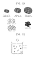
- FIGs. 2A and 2B are views showing a method for dispersing carbon nanotubes into a soldering flux according to an embodiment of the present invention.
- carbon nanotubes 22 may be evenly dispersed into a soldering flux 20.
- the carbon nanotubes 22 may comprise single-walled carbon nanotubes, double-walled carbon nanotubes, multi-walled carbon nanotubes, and nanotube ropes.
- the carbon nanotubes are classified according to a bond number.
- the carbon nanotubes may have at least one of an arm chair structure and a zigzag structure.
- the carbon nanotubes are classified according to an arrangement shape of atoms.
- the soldering flux, into which the carbon nanotubes have been dispersed, has very high conductivity.
- the method for fabricating a solar cell module according to an embodiment of the present invention may comprise spraying the soldering flux including the carbon nanotubes, onto connection parts between solar cell devices and an interconnector (S120). Also, the method for fabricating a solar cell module according to an embodiment of the present invention may comprise connecting the solar cell devices with the interconnector using the soldering flux (S130).
- FIG. 3 is a view showing a method for spraying the soldering flux onto connection parts between the solar cell devices and the interconnector, and a method for connecting the solar cell devices with the interconnector.
- the position of the solar cell devices 30 may be fixed so that the solar cell devices 30 can be connected to each other in series.
- the soldering flux 20 including the carbon nanotubes may be evenly sprayed onto connection parts between the solar cell devices and an interconnector 40 (ribbon connection parts). Then, the interconnector 40 is aligned on the positions where the soldering flux 20 has been sprayed, so that the solar cell devices 30 and the interconnector 40 are connected to each other by the soldering flux 20. In this case, an output of the solar cell module may be enhanced, because a contact resistance is lowered.
- the interconnector 40 may be implemented as a ribbon wire used in the solar cell module.
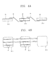
- FIGs. 4A and 4B are views showing another example to connect the solar cell devices with the interconnector.
- FIG. 4A shows a side surface of the solar cell devices and the interconnector connected to each other.
- FIG. 4B illustrates an upper surface of FIG. 4A .
- an upper surface of the solar cell device 30-1 may be serially connected to a lower surface of the solar cell device 30-2, by the interconnector 40.
- an upper surface of the solar cell device 30-2 may be serially connected to a lower surface of the solar cell device 30-3, by the interconnector 40.
- flux may be sprayed onto positions of the solar cell devices contacting the interconnector.
- flux may be sprayed onto positions of the interconnector contacting the solar cell devices.
- the present invention may be applied to a similar structure to the conventional structure for fabricating a solar cell module. Further, as various types of carbon nanotubes are applied to flux, can be reduced a resistance occurring when the ribbon is connected to the solar cell devices.
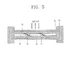
- FIG. 5 is a view showing a silicon solar cell module fabricated according to an embodiment of the present invention.
- the silicon solar cell module may comprise a surface material 50, a filling material (ethylene vinyl acetate, EVA) 60, solar cell devices 30, a filling material (ethylene vinyl acetate, EVA) 60, a back sheet surface material 70.
- EVA ethylene vinyl acetate
- EVA ethylene vinyl acetate
- the surface material 50 may be implemented as a low iron reinforcing glass, etc.
- the surface material is formed to have high transmittance, and is processed to have low optical return loss.
- the EVA serving as the filling material 60 is inserted into a space between a front surface of the solar cell devices 30 and the surface material 50, and a space between a rear surface of the solar cell devices 30 and the surface material 70, in order to protect the brittle solar cell devices.
- the EVA sheet When exposed to ultraviolet rays for a long time, the EVA sheet may discolor and may have its damp proof property lowered. Accordingly, it is important to adopt processes appropriate to characteristics of the EVS sheet when fabricating the solar cell module, so that the solar cell module can have a prolonged lifespan and an enhanced reliability.
- the back sheet surface material 70 is positioned on a rear surface of the solar cell module, and should be configured to be simply treated and to have an excellent bonding force between layers. Further, the back sheet surface material 70 should be configured to protect the solar cell module from external environments, by preventing moisture from being introduced into the solar cell module from the rear surface of the solar cell module.
- the solar cell devices 30 may be connected to each other by an interconnector.
- the interconnector may be implemented as a metallic ribbon.
- the solar cell module may comprise a sealant 80 such as a butyl rubber, and an external cover 90 formed of aluminum, etc.
- An output amount of the solar cell module may be determined according to a current amount and a voltage.
- the current amount may be proportional to an area of silicon solar cell devices, unitary devices.
- the voltage may be increased as the solar cell devices are connected with each other in series.
- the solar cell devices and the metallic ribbon are connected to each other by the soldering flux into which the carbon nanotubes of high conductivity have been dispersed. This can enhance conductivity between the solar cell devices and the metallic ribbon. As a result, an output of the solar cell module can be enhanced.
- FIGs. 6A and 6B are views showing an example to perform a photovoltaic power generation using a silicon solar cell module.
- the photovoltaic power generation indicates a method for generating power by directly converting sunlight into electricity.
- such solar cells are connected to each other in series or in parallel, to have a structure capable of enduring natural environments and external impacts for a long time.
- the minimum unit of the solar cells is called a 'photovoltaic module'.
- the photovoltaic modules may be disposed in the form of a photovoltaic array according to a substantially-used load.
- the array panels may be installed on a solar-powered house, etc.
- the embodiments described herein may be implemented within one or more of Application Specific Integrated Circuits (ASICs), Digital Signal Processors (DSPs), Digital Signal Processing Devices (DSPDs), Programmable Logic Devices (PLDs), Field Programmable Gate Arrays (FPGAs), processors, controllers, micro-controllers, micro processors, other electronic units designed to perform the functions described herein, or a selective combination thereof. In some cases, such embodiments are implemented by the controller 180.
- ASICs Application Specific Integrated Circuits
- DSPs Digital Signal Processors
- DSPDs Digital Signal Processing Devices
- PLDs Programmable Logic Devices
- FPGAs Field Programmable Gate Arrays
- processors controllers, micro-controllers, micro processors, other electronic units designed to perform the functions described herein, or a selective combination thereof.
- controller 180 such embodiments are implemented by the controller 180.
- the embodiments such as procedures and functions may be implemented together with separate software modules each of which performs at least one of functions and operations.
- the software codes can be implemented with a software application written in any suitable programming language. Also, the software codes may be stored in a memory and executed by a processor.
- the present invention can have the following advantages.
- conductivity between the solar cell devices and the ribbon can be enhanced.
- an output efficiency of the solar cell module can be enhanced.
Landscapes
- Photovoltaic Devices (AREA)
- Engineering & Computer Science (AREA)
- Manufacturing & Machinery (AREA)
Applications Claiming Priority (1)
| Application Number | Priority Date | Filing Date | Title |
|---|---|---|---|
| KR1020120048794A KR20130125220A (ko) | 2012-05-08 | 2012-05-08 | 태양 전지 모듈 및 이의 제조 방법 |
Publications (1)
| Publication Number | Publication Date |
|---|---|
| EP2662902A1 true EP2662902A1 (de) | 2013-11-13 |
Family
ID=48193203
Family Applications (1)
| Application Number | Title | Priority Date | Filing Date |
|---|---|---|---|
| EP13166633.1A Withdrawn EP2662902A1 (de) | 2012-05-08 | 2013-05-06 | Solarzellenmodul und Herstellungsverfahren davon |
Country Status (5)
| Country | Link |
|---|---|
| US (1) | US20130298960A1 (de) |
| EP (1) | EP2662902A1 (de) |
| JP (1) | JP2013236080A (de) |
| KR (1) | KR20130125220A (de) |
| CN (1) | CN103390690A (de) |
Cited By (2)
| Publication number | Priority date | Publication date | Assignee | Title |
|---|---|---|---|---|
| EP3157065A1 (de) * | 2015-10-12 | 2017-04-19 | LG Electronics Inc. | Vorrichtung und verfahren zur befestigung von verbindern eines solarzellenpaneels |
| KR20170075216A (ko) * | 2015-12-23 | 2017-07-03 | 엘지전자 주식회사 | 태양 전지 패널의 배선재 부착 장치 |
Families Citing this family (1)
| Publication number | Priority date | Publication date | Assignee | Title |
|---|---|---|---|---|
| KR102491574B1 (ko) | 2016-02-29 | 2023-01-25 | 삼성전자주식회사 | 반도체 패키지의 제조 방법 |
Citations (1)
| Publication number | Priority date | Publication date | Assignee | Title |
|---|---|---|---|---|
| US20080086876A1 (en) * | 2006-10-16 | 2008-04-17 | Mysticmd Inc. | Bondable conductive ink |
Family Cites Families (7)
| Publication number | Priority date | Publication date | Assignee | Title |
|---|---|---|---|---|
| JPH11251731A (ja) * | 1998-02-27 | 1999-09-17 | Fuji Photo Film Co Ltd | クリーム半田塗布方法 |
| JP2006049429A (ja) * | 2004-08-02 | 2006-02-16 | Sharp Corp | 太陽電池セルの製造方法および太陽電池モジュール |
| US20070145097A1 (en) * | 2005-12-20 | 2007-06-28 | Intel Corporation | Carbon nanotubes solder composite for high performance interconnect |
| WO2008143233A1 (ja) * | 2007-05-21 | 2008-11-27 | Kyoto University | フェニレン系ポリマー、カーボンナノチューブ用分散剤、カーボンナノチューブ複合体、太陽電池用薄膜、ならびにカーボンナノチューブ複合体の分散液およびその製造方法 |
| JP2009267093A (ja) * | 2008-04-25 | 2009-11-12 | Showa Shell Sekiyu Kk | 太陽電池モジュール |
| US20100175756A1 (en) * | 2009-01-15 | 2010-07-15 | Weihs Timothy P | Method For Bonding Of Concentrating Photovoltaic Receiver Module To Heat Sink Using Foil And Solder |
| US20110308573A1 (en) * | 2010-06-21 | 2011-12-22 | Fraunhofer USA, Inc. Center for Sustainable Energy Systems | Devices and methods to create a diffuse reflection surface |
-
2012
- 2012-05-08 KR KR1020120048794A patent/KR20130125220A/ko not_active Ceased
-
2013
- 2013-04-26 US US13/871,821 patent/US20130298960A1/en not_active Abandoned
- 2013-05-02 JP JP2013097012A patent/JP2013236080A/ja active Pending
- 2013-05-06 EP EP13166633.1A patent/EP2662902A1/de not_active Withdrawn
- 2013-05-08 CN CN2013101672656A patent/CN103390690A/zh active Pending
Patent Citations (1)
| Publication number | Priority date | Publication date | Assignee | Title |
|---|---|---|---|---|
| US20080086876A1 (en) * | 2006-10-16 | 2008-04-17 | Mysticmd Inc. | Bondable conductive ink |
Non-Patent Citations (2)
| Title |
|---|
| BANERJEE K ET AL: "Carbon Nanomaterials for Next-Generation Interconnects and Passives: Physics, Status, and Prospects", IEEE TRANSACTIONS ON ELECTRON DEVICES, IEEE SERVICE CENTER, PISACATAWAY, NJ, US, vol. 56, no. 9, September 2009 (2009-09-01), pages 1799 - 1821, XP011272352, ISSN: 0018-9383, DOI: 10.1109/TED.2009.2026524 * |
| YONAS ZEMEN ET AL: "Innovative and gentle interconnection technique for high efficiency c-Si solar cells and cost-of-ownership-analysis (COO)", PROCEEDINGS OF THE 26TH EUROPEAN PHOTOVOLTAIC SOLAR ENERGY CONFERENCE, 5 September 2011 (2011-09-05) - 9 September 2011 (2011-09-09), pages 3125 - 3132, XP055072272, ISBN: 3-936338-27-2, DOI: 10.4229/26thEUPVSEC2011-4CO.6.4 * |
Cited By (4)
| Publication number | Priority date | Publication date | Assignee | Title |
|---|---|---|---|---|
| EP3157065A1 (de) * | 2015-10-12 | 2017-04-19 | LG Electronics Inc. | Vorrichtung und verfahren zur befestigung von verbindern eines solarzellenpaneels |
| US10290761B2 (en) | 2015-10-12 | 2019-05-14 | Lg Electronics Inc. | Apparatus and method for attaching interconnector of solar cell panel |
| KR20170075216A (ko) * | 2015-12-23 | 2017-07-03 | 엘지전자 주식회사 | 태양 전지 패널의 배선재 부착 장치 |
| KR102487772B1 (ko) | 2015-12-23 | 2023-01-12 | 상라오 징코 솔라 테크놀러지 디벨롭먼트 컴퍼니, 리미티드 | 태양 전지 패널의 배선재 부착 장치 |
Also Published As
| Publication number | Publication date |
|---|---|
| JP2013236080A (ja) | 2013-11-21 |
| US20130298960A1 (en) | 2013-11-14 |
| KR20130125220A (ko) | 2013-11-18 |
| CN103390690A (zh) | 2013-11-13 |
Similar Documents
| Publication | Publication Date | Title |
|---|---|---|
| US10270387B2 (en) | Photovoltaic module | |
| JP5396382B2 (ja) | 太陽光発電システム用電力線およびそれを用いた太陽光発電システム | |
| WO2011093383A1 (ja) | 太陽電池モジュール | |
| EP3346507B1 (de) | Solarzellentafel | |
| JP2011176231A (ja) | 太陽電池モジュール | |
| US8664512B2 (en) | Photovoltaic module | |
| US10236823B2 (en) | Solar battery module | |
| CN103493222A (zh) | 用于防止极化的太阳能电池组件结构和制造方法 | |
| JP2005183660A (ja) | 太陽電池モジュール | |
| CN108352415A (zh) | 在太阳能电池上形成抗应力增强的前金属接触件 | |
| US20130298960A1 (en) | Solar cell module and fabrication method of the same | |
| CN101047211B (zh) | 太阳能电池组件 | |
| WO2024057855A1 (ja) | 太陽電池モジュール | |
| US20140326291A1 (en) | Solar cell module and method of fabricating the same | |
| US20110259411A1 (en) | Packaging structure and process of solar cell | |
| US20140332062A1 (en) | Solar cell apparatus | |
| KR101327014B1 (ko) | 태양전지 모듈 및 그 제조방법 | |
| US20160233345A1 (en) | Solar battery module | |
| CN104115279B (zh) | 太阳能电池组件 | |
| KR20130065493A (ko) | 태양전지 모듈 및 그 제조방법 | |
| KR101306427B1 (ko) | 태양전지 모듈 및 그 제조방법 | |
| KR20110128534A (ko) | 태양광 모듈 | |
| JP2016072518A (ja) | 太陽電池モジュール | |
| TW202549594A (zh) | 鈍化配置在至少部分地製造的太陽能模組內之複數太陽能電池的方法 | |
| JP5995104B2 (ja) | 太陽電池モジュール |
Legal Events
| Date | Code | Title | Description |
|---|---|---|---|
| PUAI | Public reference made under article 153(3) epc to a published international application that has entered the european phase |
Free format text: ORIGINAL CODE: 0009012 |
|
| AK | Designated contracting states |
Kind code of ref document: A1 Designated state(s): AL AT BE BG CH CY CZ DE DK EE ES FI FR GB GR HR HU IE IS IT LI LT LU LV MC MK MT NL NO PL PT RO RS SE SI SK SM TR |
|
| AX | Request for extension of the european patent |
Extension state: BA ME |
|
| 17P | Request for examination filed |
Effective date: 20140331 |
|
| RBV | Designated contracting states (corrected) |
Designated state(s): AL AT BE BG CH CY CZ DE DK EE ES FI FR GB GR HR HU IE IS IT LI LT LU LV MC MK MT NL NO PL PT RO RS SE SI SK SM TR |
|
| STAA | Information on the status of an ep patent application or granted ep patent |
Free format text: STATUS: REQUEST FOR EXAMINATION WAS MADE |
|
| STAA | Information on the status of an ep patent application or granted ep patent |
Free format text: STATUS: THE APPLICATION IS DEEMED TO BE WITHDRAWN |
|
| 18D | Application deemed to be withdrawn |
Effective date: 20171201 |