EP2659746B1 - Stromversorgung - Google Patents
Stromversorgung Download PDFInfo
- Publication number
- EP2659746B1 EP2659746B1 EP11853672.1A EP11853672A EP2659746B1 EP 2659746 B1 EP2659746 B1 EP 2659746B1 EP 11853672 A EP11853672 A EP 11853672A EP 2659746 B1 EP2659746 B1 EP 2659746B1
- Authority
- EP
- European Patent Office
- Prior art keywords
- light emission
- board
- boards
- current
- power supply
- Prior art date
- Legal status (The legal status is an assumption and is not a legal conclusion. Google has not performed a legal analysis and makes no representation as to the accuracy of the status listed.)
- Not-in-force
Links
Images

Classifications
-
- H—ELECTRICITY
- H05—ELECTRIC TECHNIQUES NOT OTHERWISE PROVIDED FOR
- H05B—ELECTRIC HEATING; ELECTRIC LIGHT SOURCES NOT OTHERWISE PROVIDED FOR; CIRCUIT ARRANGEMENTS FOR ELECTRIC LIGHT SOURCES, IN GENERAL
- H05B45/00—Circuit arrangements for operating light-emitting diodes [LED]
- H05B45/30—Driver circuits
- H05B45/37—Converter circuits
-
- G—PHYSICS
- G05—CONTROLLING; REGULATING
- G05F—SYSTEMS FOR REGULATING ELECTRIC OR MAGNETIC VARIABLES
- G05F1/00—Automatic systems in which deviations of an electric quantity from one or more predetermined values are detected at the output of the system and fed back to a device within the system to restore the detected quantity to its predetermined value or values, i.e. retroactive systems
- G05F1/10—Regulating voltage or current
-
- H—ELECTRICITY
- H02—GENERATION; CONVERSION OR DISTRIBUTION OF ELECTRIC POWER
- H02M—APPARATUS FOR CONVERSION BETWEEN AC AND AC, BETWEEN AC AND DC, OR BETWEEN DC AND DC, AND FOR USE WITH MAINS OR SIMILAR POWER SUPPLY SYSTEMS; CONVERSION OF DC OR AC INPUT POWER INTO SURGE OUTPUT POWER; CONTROL OR REGULATION THEREOF
- H02M3/00—Conversion of dc power input into dc power output
- H02M3/02—Conversion of dc power input into dc power output without intermediate conversion into ac
- H02M3/04—Conversion of dc power input into dc power output without intermediate conversion into ac by static converters
- H02M3/10—Conversion of dc power input into dc power output without intermediate conversion into ac by static converters using discharge tubes with control electrode or semiconductor devices with control electrode
- H02M3/145—Conversion of dc power input into dc power output without intermediate conversion into ac by static converters using discharge tubes with control electrode or semiconductor devices with control electrode using devices of a triode or transistor type requiring continuous application of a control signal
- H02M3/155—Conversion of dc power input into dc power output without intermediate conversion into ac by static converters using discharge tubes with control electrode or semiconductor devices with control electrode using devices of a triode or transistor type requiring continuous application of a control signal using semiconductor devices only
-
- H—ELECTRICITY
- H05—ELECTRIC TECHNIQUES NOT OTHERWISE PROVIDED FOR
- H05B—ELECTRIC HEATING; ELECTRIC LIGHT SOURCES NOT OTHERWISE PROVIDED FOR; CIRCUIT ARRANGEMENTS FOR ELECTRIC LIGHT SOURCES, IN GENERAL
- H05B45/00—Circuit arrangements for operating light-emitting diodes [LED]
- H05B45/30—Driver circuits
- H05B45/345—Current stabilisation; Maintaining constant current
-
- Y—GENERAL TAGGING OF NEW TECHNOLOGICAL DEVELOPMENTS; GENERAL TAGGING OF CROSS-SECTIONAL TECHNOLOGIES SPANNING OVER SEVERAL SECTIONS OF THE IPC; TECHNICAL SUBJECTS COVERED BY FORMER USPC CROSS-REFERENCE ART COLLECTIONS [XRACs] AND DIGESTS
- Y02—TECHNOLOGIES OR APPLICATIONS FOR MITIGATION OR ADAPTATION AGAINST CLIMATE CHANGE
- Y02B—CLIMATE CHANGE MITIGATION TECHNOLOGIES RELATED TO BUILDINGS, e.g. HOUSING, HOUSE APPLIANCES OR RELATED END-USER APPLICATIONS
- Y02B20/00—Energy efficient lighting technologies, e.g. halogen lamps or gas discharge lamps
- Y02B20/30—Semiconductor lamps, e.g. solid state lamps [SSL] light emitting diodes [LED] or organic LED [OLED]
Definitions
- the present disclosure relates to a power supply.
- LCDs include two display substrates where an electric field applying electrode is displayed, and a liquid crystal layer that has dielectric anisotropy and is disposed between the two substrates. LCDs apply a voltage to an electric field applying electrode to generate an electric field in a liquid crystal layer, change the voltage to adjust intensity of the electric field, and thus adjust a transmittance of light passing through the liquid crystal layer, thereby displaying a desired image.
- US 2008/0297062 A1 discloses a constant-current power supply and light emitting modules that can be connected in parallel.
- WO 2008/039024 A1 discloses a lighting device, a backlight unit and a printed circuit board thereof which can use light emitting elements and can be driven in a sub-divided manner.
- LCDs cannot self emit light, the LCDs require a separate light source called a backlight, and the light source is being replaced by Light Emitting Diodes (LEDs).
- LEDs Light Emitting Diodes
- LEDs are semiconductor devices, LEDs have long service life, fast lighting speed, low consumption power, and excellent color reproductivity. Moreover, LEDs are robust to impact, and facilitate the miniaturizing and thinning of LEDs. Therefore, a backlight using LEDs are being mounted on medium and large LCDs such as computer monitors and televisions (TVs), in addition to small LCDs mounted on mobile phones, etc.
- TVs computer monitors and televisions
- Embodiments provide a power supply with a new current regulation circuit.
- Examples also provide a power supply which automatically senses the change in the number of LEDs and varies an output current in correspondence with the change in the number of LEDs.
- Embodiments also provide a power supply which supplies a current to LEDs of each board in a constant current scheme, according to the change in the number of boards including LEDs.
- a power supply includes: a light emission module, a power source and a feedback control unit according to claim 1.
- a light emission unit including LEDs and a lighting system such as a light unit including the light emission unit can be improved in reliability.
- a current can be supplied in a constant current scheme, according to the change in the number of light emission units including LEDs or the number of boards.
- the power supply and a lighting system such as a backlight unit including the power supply can be improved in reliability.
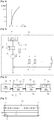
- a power supply includes a power source 101, a light emission module 120 including a plurality of boards B1 to Bn, and a feedback control unit 110.
- the power source 101 may supply an Alternating Current voltage, for example, include a switched-mode power supply (SMPS).
- the power supply includes a filter 102 that is connected to an output terminal of the power source 101 in parallel.
- the filter 102 includes a capacitor C1, and removes a ripple included in a Direct Current (DC) voltage.
- DC Direct Current
- the light emission module 120 includes the boards B1 to Bn, which may be electrically connected to each other.
- the boards B1 to Bn may be physically separated from each other, and an interval between the boards B1 to Bn may be constant.
- Each of the boards B 1 to Bn may be a flexible substrate, a rigid substrate, or a metal core Printed Circuit Board (PCB), a material of which may be resin or ceramic, but the embodiment is not limited thereto.
- PCB Printed Circuit Board
- Each of the boards B1 to Bn may include a plurality of light emission units 121 to 12n including LEDs, and a load detector 130 including a plurality of board resistors R1 to Rn that are electrically separated from the light emission units 121 to 12n.
- At least one of the light emission units 121 to 12n may be disposed on each of the boards B1 to Bn.
- a plurality of LEDs D are connected in series.
- the light emission units in each board may be connected to each other in parallel.
- Each of the LEDs D is LED emits light of a visible light band such as blue, red, green, and white, but the embodiment is not limited thereto.
- the light emission units 121 to 12n disposed on each of the boards B1 to Bn are connected to each other in parallel. That is, input terminals of the respective light emission units 121 to 12n are connected to a positive polarity terminal of the power source 101 in common, and output terminals of the respective light emission units 121 to 12n are connected to a negative polarity terminal of the power source 101 in common.
- the number of LEDs D in each of the light emission units 121 to 12n may be changed according to a voltage inputted by the power source 101, but the embodiment is not limited thereto.
- a plurality of board resistors (R1 to Rn) 131 to 13n may be respectively disposed on the boards B1 to Bn, and one board resistor may be disposed on each of the boards B1 to Bn.
- One board resistor may be disposed in each light emission unit, but the present disclosure is not limited thereto.
- the load detector 130 may include the board resistors 131 to 13n that are connected to each other in parallel, and elements such as diodes other than the board resistors may be further connected thereto. However, the embodiment is not limited thereto.
- the board resistors (R1 to Rn) 131 to 13n may be respectively disposed at a top or bottom of each of the boards B1 to Bn, and the diodes D disposed in each of the light emission units 121 to 12n may be electrically opened.
- Each of the board resistors 131 to 13n is a setting resistor for sensing whether the boards B1 to Bn, namely, the light emission units 121 to 12n are connected.
- the board resistors 131 to 13n may automatically change an input current of each of the light emission units 121 to 12n according to an output value of each of the board resistors 131 to 13n.
- the board resistors 131 to 13n may be connected to each other in parallel or in series, but the embodiment is not limited thereto.
- the number of light emission units 121 to 12n or the number of boards B1 to Bn may be sensed according to the number of board resistors 131 to 13n.
- the power supply may automatically change a current inputted to each of the light emission units 121 to 12n according to the increase or decrease in the number of light emission units 121 to 12n, thereby allowing a constant current to flow.
- Values of the respective board resistors 131 to 13n may be set arbitrarily, and set as the same value.
- the feedback control unit 110 includes a current regulator 111, a reference potential unit 112, and a comparator 113.
- the current regulator 111 is connected to output terminals of the respective light emission units 121 to 12n in common.
- the current regulator 111 senses a current, flowing into the output terminal of each of the light emission units 121 to 12n, to output a current to the power source 101.
- the current regulator 111 includes a resistor, and senses the fine change of a current flowing in the current regulator 111, thereby allowing a constant current to flow in the LEDs D of each of the light emission units 121 to 12n.
- a reference voltage 142 is inputted to one end of a first resistor 141, and another end of the first resistor 141 is connected to the reference potential unit 112.
- the reference potential unit 112 outputs a potential V2 that has passed through the first resistor 141.
- one end of the first resistor 141 and one end of each of the board resistors 131 to 13n are connected to the reference potential unit 112 in parallel.
- each of the board resistors R1 to Rn may be connected to a ground terminal.
- the first resistor 141 may be configured in another structure, for example, a diamond structure, but the embodiment is not limited thereto.
- a potential V2 of the reference potential unit 112 may be a voltage that is obtained through voltage-division with values of the respective board resistors 131 to 13n and a value of the first resistor 141.
- the value of the first resistor 141 is a fixed resistance value, and since the board resistors 131 to 13n are connected in parallel, values of the respective board resistors 131 to 13n may decrease or increase when at least one board is added or removed. As the values of the respective board resistors 131 to 13n decrease or increase, the potential V2 may increase or decrease.
- the comparator 113 compares the potential V2 of the reference potential unit 112 and a potential V3 of an input terminal of the current regulator 111, and an output V4 of the comparator 113 is inputted to the power source 101.
- the potential V3 of the input terminal of the current regulator 113 may be inputted to a positive polarity terminal of the comparator 113, and the potential V2 of the reference potential unit 112 may be inputted to a negative polarity terminal of the comparator 113.
- the comparator 113 compares the potential V2 inputted to the negative polarity terminal thereof and the potential V3 inputted to the positive polarity terminal thereof, and as the potential V2 is changed, the output V4 of the comparator 113 is changed. For example, the output V4 of the comparator 113 increases when the potential V2 decreases, but when the potential V2 increases, the output V4 of the comparator 113 decreases.
- the power source 101 regulates a current value of the DC power source according to the output V4 of the comparator 113. As the output V4 of the comparator 113 increases, the power source 101 increases a supplied current, but as the output V4 of the comparator 113 decreases, the power source 101 decreases the supplied current.
- the power source 101 automatically increases or decreases a current according to the number of connected boards B1 to Bn, thereby allowing a constant current to flow.
- the reference potential unit 112 may detect that a value of each of the board resistors 131 to 13n is changed to the level of an individual board resistance value according to the addition or removal of the boards B1 to Bn. Since the output V4 of the comparator 113 is changed according to the change of the individual board resistance value, a current supplied by the power source 101 may be regulated according to the individual board resistance value. Therefore, even if a board is added or removed, a current of a constant range may be regulated to be always supplied.
- a current which is inputted to each of the boards B1 to Bn or each of the light emission units 121 to 12n according to the output of the comparator 113 that varies by the value of each of the board resistors 131 to 13n, is supplied without change irrespective of the change of a board.
- a plurality of LEDs in each of light emission units 121 to 124 are connected in series.
- An input current I is distributed to the light emission units 121 to 124, and thus, the same level of currents I1 to I4 flow in the light emission units 121 to 124, respectively.
- the input current I is about 1000 mA
- currents I1 to I4 of about 250 mA flow in the light emission units 121 to 124, respectively.
- the currents of the respective light emission units 121 to 124 are summed in output terminals of the respective light emission units 121 to 124, and thus, an output current I of about 1000 mA is sensed.
- the reference output current is controlled as a constant current.
- a fifth light emission unit 125 is additionally connected unlike in Fig. 2 , and an input current I' is distributed and supplied to the light emission units 121 to 125.
- an input current I' is about 1000 mA
- the currents I1 to I5 of about 200mA flow in the light emission units 121 to 125, respectively.
- a current of each light emission unit increases. Such current change causes light emission to deviate from target light emission, and degrades the reliability of a lighting system such as a backlight unit.
- the currents I1 to I5 respectively flowing in the light emission units 121 to 125 are regulated to about 250 mA as in Fig. 2 .
- the load detector 125 includes the board resistors 131 and 132 disposed in each board, and a parallel resistance value of the board resistors 131 to 13n may be outputted.
- An output value of the load detector 125 may increase or decrease according to the number of the board resistors 131 to 13n. Since the board resistors R1 to Rn are connected to each other in parallel, the output value of each of the board resistors R1 to Rn becomes lower each time a board is added, but whenever a board is removed, the output value of each of the board resistors R1 to Rn becomes higher.
- the board resistors R1 to Rn may be connected to each other in parallel or in series, but the embodiment is not limited thereto.
- a current flows in a board resistor that is included in each of the four boards, in which case a lower constant current flows due to constant current characteristic.
- a board resistor disposed in the fourth board the connection of the fourth board is sensed, and an LED disposed in a light emission unit of the fourth board is sensed.
- the same number of LEDs may be set in each light emission unit.
- a value of each of the board resistors further decreases the output of the reference potential unit, and thus, the potential of the reference potential unit is further reduced.
- the reference potential of the reference potential unit is further reduced, and thus, the output of the comparator further increases.
- the output of the comparator increases, and the increased value increases by a value that is obtained by the increase in one board resistor. That is, an output deviation of the comparator increases or decreases according to the number of connected board resistors, and may be a value associated with each board resistor.
- a current that has increased by the increase in board may be further supplied, or a current that has decreased by the decrease in board may be further reduced. That is, the power supply automatically varies the output current of the power source 101, thereby allowing a constant current to flow without change according to the increase or decrease in board.
- a first connector 152 of a first board B1 is connected to a connector 151 of the power source 101, and a positive terminal and negative terminal of the first connector 151 are connected to a second connector 153.
- a board resistor 131 may be connected in parallel between a ground terminal GND and an interconnection between a connection port P1 of the first connector 152 and a connection port P2 of the second connector 153.
- resistors 131 of respective boards B 1 to Bn may be sequentially connected in parallel.
- the number of connected boards may be detected with a parallel resistance value of the board resistors 131 to 13n.
- the output value of the feedback control unit 110 may be changed.
- Connectors between the boards B1 to Bn may be directly or indirectly connected, but the embodiment is not limited thereto.
- the above-described power supply may be applied to a plurality of lighting systems such as backlight units, various kinds of display devices, headlamps, streetlamps, indoor lamps, outdoor lamps, signal lights, and lighting lamps.
- lighting systems such as backlight units, various kinds of display devices, headlamps, streetlamps, indoor lamps, outdoor lamps, signal lights, and lighting lamps.
- a light emission unit including LEDs and a lighting system such as a light unit including the light emission unit can be improved in reliability.
- a current can be supplied in a constant current scheme, according to the change in the number of light emission units including LEDs or the number of boards.
- the power supply and a lighting system such as a backlight unit including the power supply can be improved in reliability.
Claims (6)
- Leistungsversorgung, die Folgendes enthält:ein Lichtemissionsmodul, das mehrere Platinen (B1, ..., Bn) enthält;eine Leistungsquelle (101), die dem Lichtemissionsmodul eine Gleichstromspannung (DC-Spannung) zuführt; undeine Rückkopplungssteuereinheit (110), die die von der Leistungsquelle (101) zugeführte DC-Spannung entsprechend der Anzahl der Platinen (B1, ..., Bn) des Lichtemissionsmoduls variiert, wobeidie mehreren Platinen (B1, ..., Bn) miteinander elektrisch verbunden und voneinander physisch getrennt sind,jede der Platinen (B1, ..., Bn) Folgendes umfasst:eine Lichtemissionseinheit (121, ..., 12n); undeinen Platinenwiderstand (R1, ..., Rn), wobeider Platinenwiderstand (R1, ..., Rn) ein Einstellwiderstand ist, um zu erfassen, ob die Lichtemissionseinheiten (121, ..., 12n) der Platinen (B1, ..., Bn) verbunden sind,die Rückkopplungssteuereinheit (110) Folgendes umfasst:einen Widerstand (141), der mit einer Bezugsspannung (V1) verbunden ist;eine Bezugspotentialeinheit (112), die einen Spannungswert (V2), der durch Spannungsteilung der Bezugsspannung (V1) durch den Widerstand (141) und die Platinenwiderstände (R1, ..., Rn) erhalten wird, ausgibt; undeinen Komparator (113), der einen Ausgangsstrom der Leistungsquelle (101) steuert,der Spannungswert (V2) entsprechend der Anzahl der Platinen (B1, ..., Bn) des Lichtemissionsmoduls verändert wird,die Platinenwiderstände (R1, ..., Rn) miteinander elektrisch verbunden sind unddie Rückkopplungssteuereinheit (110) einen Eingangsstrom der Lichtemissionseinheiten entsprechend der Anzahl der Platinen (B1, ..., Bn) des Lichtemissionsmoduls variiert,dadurch gekennzeichnet, dassdie Platinenwiderstände (R1, ..., Rn) von den Lichtemissionseinheiten (121, ..., 12n) getrennt sind undder Komparator (113) den Spannungswert (V2), der von der Bezugspotentialeinheit (112) ausgegeben wird, mit einem Wert (V3) von einem Ausgangsanschluss in jeder der Lichtemissionseinheiten (121, ..., 12n) vergleicht, um ein Signal (V4) gemäß dem Vergleichsergebnis zur Leistungsquelle (101) auszugeben.
- Leistungsversorgung nach Anspruch 1, wobei die Lichtemissionseinheiten (121, ... 12n) jeweils mehrere miteinander in Reihe geschaltete Leuchtdioden (LEDs) besitzen.
- Leistungsversorgung nach Anspruch 2, wobei die Rückkopplungssteuereinheit (110) einen Stromregulierer (111), der mit einem Ausgangsanschluss von jeder der Lichtemissionseinheiten (121, ..., 12n) und dem Komparator (113) verbunden ist, umfasst, wobei das andere Ende der Stromregulierereinheit mit der Leistungsquelle (101) verbunden ist.
- Leistungsversorgung nach Anspruch 1, wobei jede der Platinen (B1, ..., Bn) einen Verbinder enthält, wobei der Verbinder die Platinenwiderstände (R1, ..., Rn) zueinander parallelschaltet.
- Leistungsversorgung nach Anspruch 1, wobei die Platinenwiderstände (R1, ..., Rn) denselben Widerstandswert besitzen.
- Leistungsversorgung nach Anspruch 1, wobei die Bezugspotentialeinheit mit einem Ende des Widerstandes (141) und einem Ende der Platinenwiderstände (R1, ..., Rn) parallelgeschaltet ist.
Applications Claiming Priority (2)
| Application Number | Priority Date | Filing Date | Title |
|---|---|---|---|
| KR1020100136076A KR101189313B1 (ko) | 2010-12-27 | 2010-12-27 | 전원 공급 장치 |
| PCT/KR2011/007542 WO2012091259A1 (en) | 2010-12-27 | 2011-10-11 | Power supply |
Publications (3)
| Publication Number | Publication Date |
|---|---|
| EP2659746A1 EP2659746A1 (de) | 2013-11-06 |
| EP2659746A4 EP2659746A4 (de) | 2016-06-22 |
| EP2659746B1 true EP2659746B1 (de) | 2018-12-05 |
Family
ID=46383310
Family Applications (1)
| Application Number | Title | Priority Date | Filing Date |
|---|---|---|---|
| EP11853672.1A Not-in-force EP2659746B1 (de) | 2010-12-27 | 2011-10-11 | Stromversorgung |
Country Status (7)
| Country | Link |
|---|---|
| US (1) | US9295135B2 (de) |
| EP (1) | EP2659746B1 (de) |
| JP (1) | JP6023079B2 (de) |
| KR (1) | KR101189313B1 (de) |
| CN (1) | CN103348770B (de) |
| TW (1) | TWI451802B (de) |
| WO (1) | WO2012091259A1 (de) |
Families Citing this family (7)
| Publication number | Priority date | Publication date | Assignee | Title |
|---|---|---|---|---|
| JP6037619B2 (ja) * | 2012-01-25 | 2016-12-07 | 株式会社小糸製作所 | 発光モジュールおよび車両用灯具 |
| US8963438B2 (en) | 2012-08-28 | 2015-02-24 | Micron Technology, Inc. | Self-identifying solid-state transducer modules and associated systems and methods |
| CN103851422A (zh) * | 2014-02-19 | 2014-06-11 | 北京京东方光电科技有限公司 | 用于背光源的发光组件、背光源和液晶显示装置 |
| CN106708145B (zh) * | 2017-03-30 | 2017-12-29 | 深圳市华星光电技术有限公司 | 多通道供电电路 |
| KR101987906B1 (ko) * | 2018-07-25 | 2019-06-12 | 주식회사 에스엘이디조명 | Led 개수에 따라 전원을 변환하는 전원 공급 장치 및 그의 전원 공급 제어 방법 |
| CN111064357B (zh) * | 2018-10-17 | 2021-11-02 | 上海宝存信息科技有限公司 | 电子装置电路板 |
| KR102260349B1 (ko) * | 2019-06-18 | 2021-06-03 | 박정용 | Led 조명 이상 검출 장치 |
Family Cites Families (14)
| Publication number | Priority date | Publication date | Assignee | Title |
|---|---|---|---|---|
| JP3824603B2 (ja) * | 2002-10-16 | 2006-09-20 | シーシーエス株式会社 | Led照明装置用電源システム |
| KR100786096B1 (ko) * | 2006-09-26 | 2007-12-21 | 엘지전자 주식회사 | 백라이트 유닛 및 그 인쇄회로기판 |
| JP2008108564A (ja) * | 2006-10-25 | 2008-05-08 | Matsushita Electric Works Ltd | Led点灯回路およびそれを用いる照明器具 |
| JP2008130295A (ja) * | 2006-11-17 | 2008-06-05 | Matsushita Electric Works Ltd | Led点灯回路およびそれを用いる照明器具 |
| JP4577525B2 (ja) | 2007-05-31 | 2010-11-10 | 東芝ライテック株式会社 | 照明装置 |
| CN201044524Y (zh) | 2007-06-25 | 2008-04-02 | 四川大学 | 照明发光二极管阵列的恒流和调光控制电路 |
| JP2009210484A (ja) * | 2008-03-05 | 2009-09-17 | Kenwood Corp | 集積回路等の端子接続状態監視回路 |
| CN101636028B (zh) | 2008-07-25 | 2012-10-31 | 国琏电子(上海)有限公司 | 保护电路及使用其的灯管驱动装置 |
| KR20100092696A (ko) * | 2009-02-13 | 2010-08-23 | 엘지이노텍 주식회사 | 발광 모듈 및 이를 구비한 라이트 유닛 |
| KR101048175B1 (ko) * | 2009-05-07 | 2011-07-08 | 엘지이노텍 주식회사 | Led 구동회로 |
| TWM379173U (en) * | 2009-12-07 | 2010-04-21 | Universal Optoelectronics Co Ltd | Cascaded light-emitting diode device |
| CN101778508B (zh) * | 2010-01-18 | 2012-10-31 | 友达光电股份有限公司 | 发光二极管驱动电路及驱动方法 |
| US8653738B2 (en) * | 2010-07-30 | 2014-02-18 | Shenzhen China Star Optoelectronics Technology Co. Ltd. | Backlight module |
| US8963438B2 (en) * | 2012-08-28 | 2015-02-24 | Micron Technology, Inc. | Self-identifying solid-state transducer modules and associated systems and methods |
-
2010
- 2010-12-27 KR KR1020100136076A patent/KR101189313B1/ko active IP Right Grant
-
2011
- 2011-10-03 TW TW100135775A patent/TWI451802B/zh not_active IP Right Cessation
- 2011-10-11 WO PCT/KR2011/007542 patent/WO2012091259A1/en active Application Filing
- 2011-10-11 US US13/976,610 patent/US9295135B2/en not_active Expired - Fee Related
- 2011-10-11 JP JP2013547284A patent/JP6023079B2/ja not_active Expired - Fee Related
- 2011-10-11 EP EP11853672.1A patent/EP2659746B1/de not_active Not-in-force
- 2011-10-11 CN CN201180066490.XA patent/CN103348770B/zh not_active Expired - Fee Related
Non-Patent Citations (1)
| Title |
|---|
| None * |
Also Published As
| Publication number | Publication date |
|---|---|
| US9295135B2 (en) | 2016-03-22 |
| EP2659746A4 (de) | 2016-06-22 |
| WO2012091259A1 (en) | 2012-07-05 |
| EP2659746A1 (de) | 2013-11-06 |
| CN103348770A (zh) | 2013-10-09 |
| JP6023079B2 (ja) | 2016-11-09 |
| TW201228460A (en) | 2012-07-01 |
| JP2014507754A (ja) | 2014-03-27 |
| KR101189313B1 (ko) | 2012-10-09 |
| KR20120074117A (ko) | 2012-07-05 |
| CN103348770B (zh) | 2015-07-29 |
| TWI451802B (zh) | 2014-09-01 |
| US20130271020A1 (en) | 2013-10-17 |
Similar Documents
| Publication | Publication Date | Title |
|---|---|---|
| EP2659746B1 (de) | Stromversorgung | |
| US9301370B2 (en) | Power supply for light emitting diodes (LEDs) | |
| US10396659B2 (en) | Load driving device, and lighting apparatus and liquid crystal display device using the same | |
| US7714517B2 (en) | LED driver with current sink control and applications of the same | |
| EP2536254B1 (de) | Lichtemittierende Vorrichtung und Beleuchtungsvorrichtung damit | |
| US11487310B2 (en) | Load driving device, and lighting apparatus and liquid crystal display device using the same | |
| US20120105498A1 (en) | Luminescence driving apparatus, display apparatus and driving method thereof | |
| KR20110120623A (ko) | 전기적부하의 구동회로 및 그 구동방법 | |
| US9136758B2 (en) | Voltage converting LED circuit with switched capacitor network | |
| TWI501006B (zh) | 背光單元及其驅動方法 | |
| KR101241648B1 (ko) | 전원 공급 장치 |
Legal Events
| Date | Code | Title | Description |
|---|---|---|---|
| PUAI | Public reference made under article 153(3) epc to a published international application that has entered the european phase |
Free format text: ORIGINAL CODE: 0009012 |
|
| 17P | Request for examination filed |
Effective date: 20130703 |
|
| AK | Designated contracting states |
Kind code of ref document: A1 Designated state(s): AL AT BE BG CH CY CZ DE DK EE ES FI FR GB GR HR HU IE IS IT LI LT LU LV MC MK MT NL NO PL PT RO RS SE SI SK SM TR |
|
| DAX | Request for extension of the european patent (deleted) | ||
| RA4 | Supplementary search report drawn up and despatched (corrected) |
Effective date: 20160525 |
|
| RIC1 | Information provided on ipc code assigned before grant |
Ipc: G05F 1/10 20060101ALI20160519BHEP Ipc: H05B 33/08 20060101ALI20160519BHEP Ipc: H05B 37/02 20060101AFI20160519BHEP Ipc: H02M 3/155 20060101ALI20160519BHEP |
|
| STAA | Information on the status of an ep patent application or granted ep patent |
Free format text: STATUS: EXAMINATION IS IN PROGRESS |
|
| 17Q | First examination report despatched |
Effective date: 20161209 |
|
| RAP1 | Party data changed (applicant data changed or rights of an application transferred) |
Owner name: LG INNOTEK CO., LTD. |
|
| GRAP | Despatch of communication of intention to grant a patent |
Free format text: ORIGINAL CODE: EPIDOSNIGR1 |
|
| STAA | Information on the status of an ep patent application or granted ep patent |
Free format text: STATUS: GRANT OF PATENT IS INTENDED |
|
| INTG | Intention to grant announced |
Effective date: 20180619 |
|
| GRAS | Grant fee paid |
Free format text: ORIGINAL CODE: EPIDOSNIGR3 |
|
| GRAA | (expected) grant |
Free format text: ORIGINAL CODE: 0009210 |
|
| GRAA | (expected) grant |
Free format text: ORIGINAL CODE: 0009210 |
|
| STAA | Information on the status of an ep patent application or granted ep patent |
Free format text: STATUS: THE PATENT HAS BEEN GRANTED |
|
| AK | Designated contracting states |
Kind code of ref document: B1 Designated state(s): AL AT BE BG CH CY CZ DE DK EE ES FI FR GB GR HR HU IE IS IT LI LT LU LV MC MK MT NL NO PL PT RO RS SE SI SK SM TR |
|
| REG | Reference to a national code |
Ref country code: GB Ref legal event code: FG4D |
|
| REG | Reference to a national code |
Ref country code: CH Ref legal event code: EP |
|
| REG | Reference to a national code |
Ref country code: AT Ref legal event code: REF Ref document number: 1074738 Country of ref document: AT Kind code of ref document: T Effective date: 20181215 |
|
| REG | Reference to a national code |
Ref country code: IE Ref legal event code: FG4D |
|
| REG | Reference to a national code |
Ref country code: DE Ref legal event code: R096 Ref document number: 602011054646 Country of ref document: DE |
|
| REG | Reference to a national code |
Ref country code: NL Ref legal event code: MP Effective date: 20181205 |
|
| REG | Reference to a national code |
Ref country code: AT Ref legal event code: MK05 Ref document number: 1074738 Country of ref document: AT Kind code of ref document: T Effective date: 20181205 |
|
| REG | Reference to a national code |
Ref country code: LT Ref legal event code: MG4D |
|
| PG25 | Lapsed in a contracting state [announced via postgrant information from national office to epo] |
Ref country code: BG Free format text: LAPSE BECAUSE OF FAILURE TO SUBMIT A TRANSLATION OF THE DESCRIPTION OR TO PAY THE FEE WITHIN THE PRESCRIBED TIME-LIMIT Effective date: 20190305 Ref country code: NO Free format text: LAPSE BECAUSE OF FAILURE TO SUBMIT A TRANSLATION OF THE DESCRIPTION OR TO PAY THE FEE WITHIN THE PRESCRIBED TIME-LIMIT Effective date: 20190305 Ref country code: ES Free format text: LAPSE BECAUSE OF FAILURE TO SUBMIT A TRANSLATION OF THE DESCRIPTION OR TO PAY THE FEE WITHIN THE PRESCRIBED TIME-LIMIT Effective date: 20181205 Ref country code: LT Free format text: LAPSE BECAUSE OF FAILURE TO SUBMIT A TRANSLATION OF THE DESCRIPTION OR TO PAY THE FEE WITHIN THE PRESCRIBED TIME-LIMIT Effective date: 20181205 Ref country code: LV Free format text: LAPSE BECAUSE OF FAILURE TO SUBMIT A TRANSLATION OF THE DESCRIPTION OR TO PAY THE FEE WITHIN THE PRESCRIBED TIME-LIMIT Effective date: 20181205 Ref country code: AT Free format text: LAPSE BECAUSE OF FAILURE TO SUBMIT A TRANSLATION OF THE DESCRIPTION OR TO PAY THE FEE WITHIN THE PRESCRIBED TIME-LIMIT Effective date: 20181205 Ref country code: HR Free format text: LAPSE BECAUSE OF FAILURE TO SUBMIT A TRANSLATION OF THE DESCRIPTION OR TO PAY THE FEE WITHIN THE PRESCRIBED TIME-LIMIT Effective date: 20181205 Ref country code: FI Free format text: LAPSE BECAUSE OF FAILURE TO SUBMIT A TRANSLATION OF THE DESCRIPTION OR TO PAY THE FEE WITHIN THE PRESCRIBED TIME-LIMIT Effective date: 20181205 |
|
| PG25 | Lapsed in a contracting state [announced via postgrant information from national office to epo] |
Ref country code: SE Free format text: LAPSE BECAUSE OF FAILURE TO SUBMIT A TRANSLATION OF THE DESCRIPTION OR TO PAY THE FEE WITHIN THE PRESCRIBED TIME-LIMIT Effective date: 20181205 Ref country code: AL Free format text: LAPSE BECAUSE OF FAILURE TO SUBMIT A TRANSLATION OF THE DESCRIPTION OR TO PAY THE FEE WITHIN THE PRESCRIBED TIME-LIMIT Effective date: 20181205 Ref country code: GR Free format text: LAPSE BECAUSE OF FAILURE TO SUBMIT A TRANSLATION OF THE DESCRIPTION OR TO PAY THE FEE WITHIN THE PRESCRIBED TIME-LIMIT Effective date: 20190306 Ref country code: RS Free format text: LAPSE BECAUSE OF FAILURE TO SUBMIT A TRANSLATION OF THE DESCRIPTION OR TO PAY THE FEE WITHIN THE PRESCRIBED TIME-LIMIT Effective date: 20181205 |
|
| PG25 | Lapsed in a contracting state [announced via postgrant information from national office to epo] |
Ref country code: NL Free format text: LAPSE BECAUSE OF FAILURE TO SUBMIT A TRANSLATION OF THE DESCRIPTION OR TO PAY THE FEE WITHIN THE PRESCRIBED TIME-LIMIT Effective date: 20181205 |
|
| PG25 | Lapsed in a contracting state [announced via postgrant information from national office to epo] |
Ref country code: IT Free format text: LAPSE BECAUSE OF FAILURE TO SUBMIT A TRANSLATION OF THE DESCRIPTION OR TO PAY THE FEE WITHIN THE PRESCRIBED TIME-LIMIT Effective date: 20181205 Ref country code: PL Free format text: LAPSE BECAUSE OF FAILURE TO SUBMIT A TRANSLATION OF THE DESCRIPTION OR TO PAY THE FEE WITHIN THE PRESCRIBED TIME-LIMIT Effective date: 20181205 Ref country code: PT Free format text: LAPSE BECAUSE OF FAILURE TO SUBMIT A TRANSLATION OF THE DESCRIPTION OR TO PAY THE FEE WITHIN THE PRESCRIBED TIME-LIMIT Effective date: 20190405 Ref country code: CZ Free format text: LAPSE BECAUSE OF FAILURE TO SUBMIT A TRANSLATION OF THE DESCRIPTION OR TO PAY THE FEE WITHIN THE PRESCRIBED TIME-LIMIT Effective date: 20181205 |
|
| PG25 | Lapsed in a contracting state [announced via postgrant information from national office to epo] |
Ref country code: EE Free format text: LAPSE BECAUSE OF FAILURE TO SUBMIT A TRANSLATION OF THE DESCRIPTION OR TO PAY THE FEE WITHIN THE PRESCRIBED TIME-LIMIT Effective date: 20181205 Ref country code: SM Free format text: LAPSE BECAUSE OF FAILURE TO SUBMIT A TRANSLATION OF THE DESCRIPTION OR TO PAY THE FEE WITHIN THE PRESCRIBED TIME-LIMIT Effective date: 20181205 Ref country code: IS Free format text: LAPSE BECAUSE OF FAILURE TO SUBMIT A TRANSLATION OF THE DESCRIPTION OR TO PAY THE FEE WITHIN THE PRESCRIBED TIME-LIMIT Effective date: 20190405 Ref country code: RO Free format text: LAPSE BECAUSE OF FAILURE TO SUBMIT A TRANSLATION OF THE DESCRIPTION OR TO PAY THE FEE WITHIN THE PRESCRIBED TIME-LIMIT Effective date: 20181205 Ref country code: SK Free format text: LAPSE BECAUSE OF FAILURE TO SUBMIT A TRANSLATION OF THE DESCRIPTION OR TO PAY THE FEE WITHIN THE PRESCRIBED TIME-LIMIT Effective date: 20181205 |
|
| REG | Reference to a national code |
Ref country code: DE Ref legal event code: R097 Ref document number: 602011054646 Country of ref document: DE |
|
| PLBE | No opposition filed within time limit |
Free format text: ORIGINAL CODE: 0009261 |
|
| STAA | Information on the status of an ep patent application or granted ep patent |
Free format text: STATUS: NO OPPOSITION FILED WITHIN TIME LIMIT |
|
| PG25 | Lapsed in a contracting state [announced via postgrant information from national office to epo] |
Ref country code: DK Free format text: LAPSE BECAUSE OF FAILURE TO SUBMIT A TRANSLATION OF THE DESCRIPTION OR TO PAY THE FEE WITHIN THE PRESCRIBED TIME-LIMIT Effective date: 20181205 Ref country code: SI Free format text: LAPSE BECAUSE OF FAILURE TO SUBMIT A TRANSLATION OF THE DESCRIPTION OR TO PAY THE FEE WITHIN THE PRESCRIBED TIME-LIMIT Effective date: 20181205 |
|
| 26N | No opposition filed |
Effective date: 20190906 |
|
| PG25 | Lapsed in a contracting state [announced via postgrant information from national office to epo] |
Ref country code: TR Free format text: LAPSE BECAUSE OF FAILURE TO SUBMIT A TRANSLATION OF THE DESCRIPTION OR TO PAY THE FEE WITHIN THE PRESCRIBED TIME-LIMIT Effective date: 20181205 |
|
| REG | Reference to a national code |
Ref country code: DE Ref legal event code: R119 Ref document number: 602011054646 Country of ref document: DE |
|
| PG25 | Lapsed in a contracting state [announced via postgrant information from national office to epo] |
Ref country code: MC Free format text: LAPSE BECAUSE OF FAILURE TO SUBMIT A TRANSLATION OF THE DESCRIPTION OR TO PAY THE FEE WITHIN THE PRESCRIBED TIME-LIMIT Effective date: 20181205 |
|
| REG | Reference to a national code |
Ref country code: CH Ref legal event code: PL |
|
| PG25 | Lapsed in a contracting state [announced via postgrant information from national office to epo] |
Ref country code: LI Free format text: LAPSE BECAUSE OF NON-PAYMENT OF DUE FEES Effective date: 20191031 Ref country code: LU Free format text: LAPSE BECAUSE OF NON-PAYMENT OF DUE FEES Effective date: 20191011 Ref country code: CH Free format text: LAPSE BECAUSE OF NON-PAYMENT OF DUE FEES Effective date: 20191031 Ref country code: DE Free format text: LAPSE BECAUSE OF NON-PAYMENT OF DUE FEES Effective date: 20200501 |
|
| REG | Reference to a national code |
Ref country code: BE Ref legal event code: MM Effective date: 20191031 |
|
| PG25 | Lapsed in a contracting state [announced via postgrant information from national office to epo] |
Ref country code: BE Free format text: LAPSE BECAUSE OF NON-PAYMENT OF DUE FEES Effective date: 20191031 |
|
| GBPC | Gb: european patent ceased through non-payment of renewal fee |
Effective date: 20191011 |
|
| PG25 | Lapsed in a contracting state [announced via postgrant information from national office to epo] |
Ref country code: IE Free format text: LAPSE BECAUSE OF NON-PAYMENT OF DUE FEES Effective date: 20191011 Ref country code: GB Free format text: LAPSE BECAUSE OF NON-PAYMENT OF DUE FEES Effective date: 20191011 Ref country code: FR Free format text: LAPSE BECAUSE OF NON-PAYMENT OF DUE FEES Effective date: 20191031 |
|
| PG25 | Lapsed in a contracting state [announced via postgrant information from national office to epo] |
Ref country code: CY Free format text: LAPSE BECAUSE OF FAILURE TO SUBMIT A TRANSLATION OF THE DESCRIPTION OR TO PAY THE FEE WITHIN THE PRESCRIBED TIME-LIMIT Effective date: 20181205 |
|
| PG25 | Lapsed in a contracting state [announced via postgrant information from national office to epo] |
Ref country code: HU Free format text: LAPSE BECAUSE OF FAILURE TO SUBMIT A TRANSLATION OF THE DESCRIPTION OR TO PAY THE FEE WITHIN THE PRESCRIBED TIME-LIMIT; INVALID AB INITIO Effective date: 20111011 Ref country code: MT Free format text: LAPSE BECAUSE OF FAILURE TO SUBMIT A TRANSLATION OF THE DESCRIPTION OR TO PAY THE FEE WITHIN THE PRESCRIBED TIME-LIMIT Effective date: 20181205 |
|
| PG25 | Lapsed in a contracting state [announced via postgrant information from national office to epo] |
Ref country code: MK Free format text: LAPSE BECAUSE OF FAILURE TO SUBMIT A TRANSLATION OF THE DESCRIPTION OR TO PAY THE FEE WITHIN THE PRESCRIBED TIME-LIMIT Effective date: 20181205 |