EP2656412B1 - Organisches halbleiterbauelement mit dotierter lochleiterschicht - Google Patents
Organisches halbleiterbauelement mit dotierter lochleiterschicht Download PDFInfo
- Publication number
- EP2656412B1 EP2656412B1 EP12700039.6A EP12700039A EP2656412B1 EP 2656412 B1 EP2656412 B1 EP 2656412B1 EP 12700039 A EP12700039 A EP 12700039A EP 2656412 B1 EP2656412 B1 EP 2656412B1
- Authority
- EP
- European Patent Office
- Prior art keywords
- hole conductor
- conductor layer
- tfms
- bis
- doping
- Prior art date
- Legal status (The legal status is an assumption and is not a legal conclusion. Google has not performed a legal analysis and makes no representation as to the accuracy of the status listed.)
- Active
Links
- 239000004020 conductor Substances 0.000 title claims description 50
- 239000004065 semiconductor Substances 0.000 title claims description 22
- 150000003839 salts Chemical class 0.000 claims description 42
- 239000002019 doping agent Substances 0.000 claims description 41
- 239000003930 superacid Substances 0.000 claims description 41
- 239000011159 matrix material Substances 0.000 claims description 25
- 238000010521 absorption reaction Methods 0.000 claims description 15
- 238000004519 manufacturing process Methods 0.000 claims description 15
- QRUBYZBWAOOHSV-UHFFFAOYSA-M silver trifluoromethanesulfonate Chemical compound [Ag+].[O-]S(=O)(=O)C(F)(F)F QRUBYZBWAOOHSV-UHFFFAOYSA-M 0.000 claims description 11
- 238000000151 deposition Methods 0.000 claims description 9
- JPVYNHNXODAKFH-UHFFFAOYSA-N Cu2+ Chemical compound [Cu+2] JPVYNHNXODAKFH-UHFFFAOYSA-N 0.000 claims description 8
- 239000002253 acid Substances 0.000 claims description 8
- SBTSVTLGWRLWOD-UHFFFAOYSA-L copper(ii) triflate Chemical compound [Cu+2].[O-]S(=O)(=O)C(F)(F)F.[O-]S(=O)(=O)C(F)(F)F SBTSVTLGWRLWOD-UHFFFAOYSA-L 0.000 claims description 8
- 230000008021 deposition Effects 0.000 claims description 8
- 238000001704 evaporation Methods 0.000 claims description 6
- 230000008020 evaporation Effects 0.000 claims description 6
- QAOWNCQODCNURD-UHFFFAOYSA-N Sulfuric acid Chemical compound OS(O)(=O)=O QAOWNCQODCNURD-UHFFFAOYSA-N 0.000 claims description 4
- 238000002207 thermal evaporation Methods 0.000 claims description 2
- 230000002378 acidificating effect Effects 0.000 claims 1
- ITMCEJHCFYSIIV-UHFFFAOYSA-N triflic acid Chemical compound OS(=O)(=O)C(F)(F)F ITMCEJHCFYSIIV-UHFFFAOYSA-N 0.000 description 52
- 239000010949 copper Substances 0.000 description 28
- 239000000463 material Substances 0.000 description 11
- 230000008901 benefit Effects 0.000 description 10
- 150000001768 cations Chemical class 0.000 description 10
- 230000000694 effects Effects 0.000 description 9
- YXFVVABEGXRONW-UHFFFAOYSA-N Toluene Chemical compound CC1=CC=CC=C1 YXFVVABEGXRONW-UHFFFAOYSA-N 0.000 description 8
- 238000010586 diagram Methods 0.000 description 8
- 230000005525 hole transport Effects 0.000 description 8
- 238000001228 spectrum Methods 0.000 description 8
- 239000000758 substrate Substances 0.000 description 8
- WEVYAHXRMPXWCK-UHFFFAOYSA-N Acetonitrile Chemical compound CC#N WEVYAHXRMPXWCK-UHFFFAOYSA-N 0.000 description 7
- UHOVQNZJYSORNB-UHFFFAOYSA-N Benzene Chemical compound C1=CC=CC=C1 UHOVQNZJYSORNB-UHFFFAOYSA-N 0.000 description 7
- 238000002347 injection Methods 0.000 description 7
- 239000007924 injection Substances 0.000 description 7
- 239000012071 phase Substances 0.000 description 7
- 239000007983 Tris buffer Substances 0.000 description 6
- 229910052751 metal Inorganic materials 0.000 description 6
- 239000002184 metal Substances 0.000 description 6
- 239000000203 mixture Substances 0.000 description 6
- 229910052782 aluminium Inorganic materials 0.000 description 5
- 238000005259 measurement Methods 0.000 description 5
- 229910052709 silver Inorganic materials 0.000 description 5
- 238000000859 sublimation Methods 0.000 description 5
- 230000008022 sublimation Effects 0.000 description 5
- HEDRZPFGACZZDS-UHFFFAOYSA-N Chloroform Chemical compound ClC(Cl)Cl HEDRZPFGACZZDS-UHFFFAOYSA-N 0.000 description 4
- 238000000862 absorption spectrum Methods 0.000 description 4
- 229910052784 alkaline earth metal Inorganic materials 0.000 description 4
- XAGFODPZIPBFFR-UHFFFAOYSA-N aluminium Chemical compound [Al] XAGFODPZIPBFFR-UHFFFAOYSA-N 0.000 description 4
- 230000015572 biosynthetic process Effects 0.000 description 4
- 229910052802 copper Inorganic materials 0.000 description 4
- 239000007791 liquid phase Substances 0.000 description 4
- 238000000103 photoluminescence spectrum Methods 0.000 description 4
- RYGMFSIKBFXOCR-UHFFFAOYSA-N Copper Chemical compound [Cu] RYGMFSIKBFXOCR-UHFFFAOYSA-N 0.000 description 3
- -1 Lanthanoid cations Chemical class 0.000 description 3
- 150000001342 alkaline earth metals Chemical class 0.000 description 3
- 150000001450 anions Chemical class 0.000 description 3
- RDOXTESZEPMUJZ-UHFFFAOYSA-N anisole Chemical compound COC1=CC=CC=C1 RDOXTESZEPMUJZ-UHFFFAOYSA-N 0.000 description 3
- 239000002585 base Substances 0.000 description 3
- 239000002800 charge carrier Substances 0.000 description 3
- MVPPADPHJFYWMZ-UHFFFAOYSA-N chlorobenzene Chemical compound ClC1=CC=CC=C1 MVPPADPHJFYWMZ-UHFFFAOYSA-N 0.000 description 3
- 125000004093 cyano group Chemical group *C#N 0.000 description 3
- 230000003287 optical effect Effects 0.000 description 3
- 239000000126 substance Substances 0.000 description 3
- 229910052723 transition metal Inorganic materials 0.000 description 3
- 150000003624 transition metals Chemical class 0.000 description 3
- RYHBNJHYFVUHQT-UHFFFAOYSA-N 1,4-Dioxane Chemical compound C1COCCO1 RYHBNJHYFVUHQT-UHFFFAOYSA-N 0.000 description 2
- XOYZGLGJSAZOAG-UHFFFAOYSA-N 1-n,1-n,4-n-triphenyl-4-n-[4-[4-(n-[4-(n-phenylanilino)phenyl]anilino)phenyl]phenyl]benzene-1,4-diamine Chemical compound C1=CC=CC=C1N(C=1C=CC(=CC=1)N(C=1C=CC=CC=1)C=1C=CC(=CC=1)C=1C=CC(=CC=1)N(C=1C=CC=CC=1)C=1C=CC(=CC=1)N(C=1C=CC=CC=1)C=1C=CC=CC=1)C1=CC=CC=C1 XOYZGLGJSAZOAG-UHFFFAOYSA-N 0.000 description 2
- IYZMXHQDXZKNCY-UHFFFAOYSA-N 1-n,1-n-diphenyl-4-n,4-n-bis[4-(n-phenylanilino)phenyl]benzene-1,4-diamine Chemical compound C1=CC=CC=C1N(C=1C=CC(=CC=1)N(C=1C=CC(=CC=1)N(C=1C=CC=CC=1)C=1C=CC=CC=1)C=1C=CC(=CC=1)N(C=1C=CC=CC=1)C=1C=CC=CC=1)C1=CC=CC=C1 IYZMXHQDXZKNCY-UHFFFAOYSA-N 0.000 description 2
- QVDYERLGSGAPKP-UHFFFAOYSA-N 1-n,4-n-dinaphthalen-2-yl-1-n,4-n-diphenylbenzene-1,4-diamine Chemical compound C1=CC=CC=C1N(C=1C=C2C=CC=CC2=CC=1)C1=CC=C(N(C=2C=CC=CC=2)C=2C=C3C=CC=CC3=CC=2)C=C1 QVDYERLGSGAPKP-UHFFFAOYSA-N 0.000 description 2
- MGNMGUIBVXLCKB-UHFFFAOYSA-N 1-n-[4-[4-(n-[4-(2-methyl-n-(2-methylphenyl)anilino)phenyl]anilino)phenyl]phenyl]-4-n,4-n-bis(2-methylphenyl)-1-n-phenylbenzene-1,4-diamine Chemical compound CC1=CC=CC=C1N(C=1C(=CC=CC=1)C)C1=CC=C(N(C=2C=CC=CC=2)C=2C=CC(=CC=2)C=2C=CC(=CC=2)N(C=2C=CC=CC=2)C=2C=CC(=CC=2)N(C=2C(=CC=CC=2)C)C=2C(=CC=CC=2)C)C=C1 MGNMGUIBVXLCKB-UHFFFAOYSA-N 0.000 description 2
- 125000001637 1-naphthyl group Chemical group [H]C1=C([H])C([H])=C2C(*)=C([H])C([H])=C([H])C2=C1[H] 0.000 description 2
- MQRCTQVBZYBPQE-UHFFFAOYSA-N 189363-47-1 Chemical compound C1=CC=CC=C1N(C=1C=C2C3(C4=CC(=CC=C4C2=CC=1)N(C=1C=CC=CC=1)C=1C=CC=CC=1)C1=CC(=CC=C1C1=CC=C(C=C13)N(C=1C=CC=CC=1)C=1C=CC=CC=1)N(C=1C=CC=CC=1)C=1C=CC=CC=1)C1=CC=CC=C1 MQRCTQVBZYBPQE-UHFFFAOYSA-N 0.000 description 2
- SRFFBQASROQQJB-UHFFFAOYSA-N 2-N',2-N',7-N',7-N'-tetrakis(9,9'-spirobi[fluorene]-2-yl)-9,9'-spirobi[fluorene]-2',7'-diamine Chemical compound C12=CC=CC=C2C2=CC=CC=C2C1(C1=C2)C3=CC=CC=C3C1=CC=C2N(C=1C=C2C3(C4=CC=CC=C4C4=CC=CC=C43)C3=CC=CC=C3C2=CC=1)C(C=C1C2(C3=CC=CC=C3C3=CC=CC=C32)C2=C3)=CC=C1C2=CC=C3N(C=1C=C2C3(C4=CC=CC=C4C4=CC=CC=C43)C3=CC=CC=C3C2=CC=1)C(C=C12)=CC=C2C2=CC=CC=C2C21C1=CC=CC=C1C1=CC=CC=C21 SRFFBQASROQQJB-UHFFFAOYSA-N 0.000 description 2
- KSSABTOENVKMLW-UHFFFAOYSA-N 2-N,2-N,2-N',2-N'-tetrakis(4-phenylphenyl)-9,9'-spirobi[fluorene]-2,2'-diamine Chemical compound C1=CC=CC=C1C1=CC=C(N(C=2C=CC(=CC=2)C=2C=CC=CC=2)C=2C=C3C4(C5=CC(=CC=C5C5=CC=CC=C54)N(C=4C=CC(=CC=4)C=4C=CC=CC=4)C=4C=CC(=CC=4)C=4C=CC=CC=4)C4=CC=CC=C4C3=CC=2)C=C1 KSSABTOENVKMLW-UHFFFAOYSA-N 0.000 description 2
- IXHWGNYCZPISET-UHFFFAOYSA-N 2-[4-(dicyanomethylidene)-2,3,5,6-tetrafluorocyclohexa-2,5-dien-1-ylidene]propanedinitrile Chemical compound FC1=C(F)C(=C(C#N)C#N)C(F)=C(F)C1=C(C#N)C#N IXHWGNYCZPISET-UHFFFAOYSA-N 0.000 description 2
- LZHVTCXAXYYCIF-UHFFFAOYSA-N 2-n',2-n',7-n',7-n'-tetrakis(4-methoxyphenyl)-9,9'-spirobi[fluorene]-2',7'-diamine Chemical compound C1=CC(OC)=CC=C1N(C=1C=C2C3(C4=CC=CC=C4C4=CC=CC=C43)C3=CC(=CC=C3C2=CC=1)N(C=1C=CC(OC)=CC=1)C=1C=CC(OC)=CC=1)C1=CC=C(OC)C=C1 LZHVTCXAXYYCIF-UHFFFAOYSA-N 0.000 description 2
- QZTQQBIGSZWRGI-UHFFFAOYSA-N 2-n',7-n'-bis(3-methylphenyl)-2-n',7-n'-diphenyl-9,9'-spirobi[fluorene]-2',7'-diamine Chemical compound CC1=CC=CC(N(C=2C=CC=CC=2)C=2C=C3C4(C5=CC=CC=C5C5=CC=CC=C54)C4=CC(=CC=C4C3=CC=2)N(C=2C=CC=CC=2)C=2C=C(C)C=CC=2)=C1 QZTQQBIGSZWRGI-UHFFFAOYSA-N 0.000 description 2
- ZDAWFMCVTXSZTC-UHFFFAOYSA-N 2-n',7-n'-dinaphthalen-1-yl-2-n',7-n'-diphenyl-9,9'-spirobi[fluorene]-2',7'-diamine Chemical compound C1=CC=CC=C1N(C=1C2=CC=CC=C2C=CC=1)C1=CC=C(C=2C(=CC(=CC=2)N(C=2C=CC=CC=2)C=2C3=CC=CC=C3C=CC=2)C23C4=CC=CC=C4C4=CC=CC=C43)C2=C1 ZDAWFMCVTXSZTC-UHFFFAOYSA-N 0.000 description 2
- BXSXNLBKCNVUGA-UHFFFAOYSA-N 2-n,2-n,2-n',2-n'-tetrakis(4-methoxyphenyl)-9,9'-spirobi[fluorene]-2,2'-diamine Chemical compound C1=CC(OC)=CC=C1N(C=1C=C2C3(C4=CC(=CC=C4C4=CC=CC=C43)N(C=3C=CC(OC)=CC=3)C=3C=CC(OC)=CC=3)C3=CC=CC=C3C2=CC=1)C1=CC=C(OC)C=C1 BXSXNLBKCNVUGA-UHFFFAOYSA-N 0.000 description 2
- ZOSISXPKNIMGRP-UHFFFAOYSA-N 2-n,2-n,2-n',2-n'-tetraphenyl-9,9'-spirobi[fluorene]-2,2'-diamine Chemical compound C1=CC=CC=C1N(C=1C=C2C3(C4=CC(=CC=C4C4=CC=CC=C43)N(C=3C=CC=CC=3)C=3C=CC=CC=3)C3=CC=CC=C3C2=CC=1)C1=CC=CC=C1 ZOSISXPKNIMGRP-UHFFFAOYSA-N 0.000 description 2
- NFZUWPDINLFCGG-UHFFFAOYSA-N 2-n,7-n-bis(3-methylphenyl)-2-n,7-n,9,9-tetraphenylfluorene-2,7-diamine Chemical compound CC1=CC=CC(N(C=2C=CC=CC=2)C=2C=C3C(C4=CC(=CC=C4C3=CC=2)N(C=2C=CC=CC=2)C=2C=C(C)C=CC=2)(C=2C=CC=CC=2)C=2C=CC=CC=2)=C1 NFZUWPDINLFCGG-UHFFFAOYSA-N 0.000 description 2
- PQCAURRJHOJJNQ-UHFFFAOYSA-N 2-n,7-n-dinaphthalen-1-yl-2-n,7-n,9,9-tetraphenylfluorene-2,7-diamine Chemical compound C1=CC=CC=C1N(C=1C2=CC=CC=C2C=CC=1)C1=CC=C(C=2C(=CC(=CC=2)N(C=2C=CC=CC=2)C=2C3=CC=CC=C3C=CC=2)C2(C=3C=CC=CC=3)C=3C=CC=CC=3)C2=C1 PQCAURRJHOJJNQ-UHFFFAOYSA-N 0.000 description 2
- HONWGFNQCPRRFM-UHFFFAOYSA-N 2-n-(3-methylphenyl)-1-n,1-n,2-n-triphenylbenzene-1,2-diamine Chemical compound CC1=CC=CC(N(C=2C=CC=CC=2)C=2C(=CC=CC=2)N(C=2C=CC=CC=2)C=2C=CC=CC=2)=C1 HONWGFNQCPRRFM-UHFFFAOYSA-N 0.000 description 2
- CCTFMNIEFHGTDU-UHFFFAOYSA-N 3-methoxypropyl acetate Chemical compound COCCCOC(C)=O CCTFMNIEFHGTDU-UHFFFAOYSA-N 0.000 description 2
- OGGKVJMNFFSDEV-UHFFFAOYSA-N 3-methyl-n-[4-[4-(n-(3-methylphenyl)anilino)phenyl]phenyl]-n-phenylaniline Chemical compound CC1=CC=CC(N(C=2C=CC=CC=2)C=2C=CC(=CC=2)C=2C=CC(=CC=2)N(C=2C=CC=CC=2)C=2C=C(C)C=CC=2)=C1 OGGKVJMNFFSDEV-UHFFFAOYSA-N 0.000 description 2
- WPUSEOSICYGUEW-UHFFFAOYSA-N 4-[4-(4-methoxy-n-(4-methoxyphenyl)anilino)phenyl]-n,n-bis(4-methoxyphenyl)aniline Chemical compound C1=CC(OC)=CC=C1N(C=1C=CC(=CC=1)C=1C=CC(=CC=1)N(C=1C=CC(OC)=CC=1)C=1C=CC(OC)=CC=1)C1=CC=C(OC)C=C1 WPUSEOSICYGUEW-UHFFFAOYSA-N 0.000 description 2
- NXVNUSIHWZLMGF-UHFFFAOYSA-N 4-phenyl-N-(4-phenylphenyl)-N-[4-[9-[4-(4-phenyl-N-(4-phenylphenyl)anilino)phenyl]fluoren-9-yl]phenyl]aniline Chemical compound C1=CC=CC=C1C1=CC=C(N(C=2C=CC(=CC=2)C=2C=CC=CC=2)C=2C=CC(=CC=2)C2(C3=CC=CC=C3C3=CC=CC=C32)C=2C=CC(=CC=2)N(C=2C=CC(=CC=2)C=2C=CC=CC=2)C=2C=CC(=CC=2)C=2C=CC=CC=2)C=C1 NXVNUSIHWZLMGF-UHFFFAOYSA-N 0.000 description 2
- YUBXDAMWVRMLOG-UHFFFAOYSA-N 9,9-dimethyl-2-n,7-n-bis(3-methylphenyl)-2-n,7-n-diphenylfluorene-2,7-diamine Chemical compound CC1=CC=CC(N(C=2C=CC=CC=2)C=2C=C3C(C)(C)C4=CC(=CC=C4C3=CC=2)N(C=2C=CC=CC=2)C=2C=C(C)C=CC=2)=C1 YUBXDAMWVRMLOG-UHFFFAOYSA-N 0.000 description 2
- KJEQVQJWXVHKGT-UHFFFAOYSA-N 9,9-dimethyl-2-n,7-n-dinaphthalen-1-yl-2-n,7-n-diphenylfluorene-2,7-diamine Chemical compound C1=C2C(C)(C)C3=CC(N(C=4C=CC=CC=4)C=4C5=CC=CC=C5C=CC=4)=CC=C3C2=CC=C1N(C=1C2=CC=CC=C2C=CC=1)C1=CC=CC=C1 KJEQVQJWXVHKGT-UHFFFAOYSA-N 0.000 description 2
- LFIYMKYMOHCZMO-UHFFFAOYSA-N C1=CC=CC=C1N(C=1C2=CC=CC=C2C=CC=1)C1=CC=C(C=2C(=CC(=CC=2)N(C=2C=CC=CC=2)C=2C3=CC=CC=C3C=CC=2)C23C4=CC(=CC=C4C4=CC=C(C=C42)N(C=2C=CC=CC=2)C=2C4=CC=CC=C4C=CC=2)N(C=2C=CC=CC=2)C=2C4=CC=CC=C4C=CC=2)C3=C1 Chemical compound C1=CC=CC=C1N(C=1C2=CC=CC=C2C=CC=1)C1=CC=C(C=2C(=CC(=CC=2)N(C=2C=CC=CC=2)C=2C3=CC=CC=C3C=CC=2)C23C4=CC(=CC=C4C4=CC=C(C=C42)N(C=2C=CC=CC=2)C=2C4=CC=CC=C4C=CC=2)N(C=2C=CC=CC=2)C=2C4=CC=CC=C4C=CC=2)C3=C1 LFIYMKYMOHCZMO-UHFFFAOYSA-N 0.000 description 2
- 229910052684 Cerium Inorganic materials 0.000 description 2
- 229910052692 Dysprosium Inorganic materials 0.000 description 2
- 229910052691 Erbium Inorganic materials 0.000 description 2
- 229910052693 Europium Inorganic materials 0.000 description 2
- 229910052688 Gadolinium Inorganic materials 0.000 description 2
- 229910052689 Holmium Inorganic materials 0.000 description 2
- 229910052765 Lutetium Inorganic materials 0.000 description 2
- 229910052779 Neodymium Inorganic materials 0.000 description 2
- 229920001609 Poly(3,4-ethylenedioxythiophene) Polymers 0.000 description 2
- 229910052777 Praseodymium Inorganic materials 0.000 description 2
- 229910052772 Samarium Inorganic materials 0.000 description 2
- VYPSYNLAJGMNEJ-UHFFFAOYSA-N Silicium dioxide Chemical compound O=[Si]=O VYPSYNLAJGMNEJ-UHFFFAOYSA-N 0.000 description 2
- BQCADISMDOOEFD-UHFFFAOYSA-N Silver Chemical compound [Ag] BQCADISMDOOEFD-UHFFFAOYSA-N 0.000 description 2
- 229910052771 Terbium Inorganic materials 0.000 description 2
- 229910052775 Thulium Inorganic materials 0.000 description 2
- GWEVSGVZZGPLCZ-UHFFFAOYSA-N Titan oxide Chemical compound O=[Ti]=O GWEVSGVZZGPLCZ-UHFFFAOYSA-N 0.000 description 2
- 229910052769 Ytterbium Inorganic materials 0.000 description 2
- 239000000370 acceptor Substances 0.000 description 2
- 150000007513 acids Chemical class 0.000 description 2
- 239000004305 biphenyl Substances 0.000 description 2
- 229920000547 conjugated polymer Polymers 0.000 description 2
- YNYHGRUPNQLZHB-UHFFFAOYSA-M copper(1+);trifluoromethanesulfonate Chemical compound [Cu+].[O-]S(=O)(=O)C(F)(F)F YNYHGRUPNQLZHB-UHFFFAOYSA-M 0.000 description 2
- 230000007423 decrease Effects 0.000 description 2
- 239000011521 glass Substances 0.000 description 2
- RBTKNAXYKSUFRK-UHFFFAOYSA-N heliogen blue Chemical compound [Cu].[N-]1C2=C(C=CC=C3)C3=C1N=C([N-]1)C3=CC=CC=C3C1=NC([N-]1)=C(C=CC=C3)C3=C1N=C([N-]1)C3=CC=CC=C3C1=N2 RBTKNAXYKSUFRK-UHFFFAOYSA-N 0.000 description 2
- 229910052746 lanthanum Inorganic materials 0.000 description 2
- 239000003446 ligand Substances 0.000 description 2
- 238000000034 method Methods 0.000 description 2
- QKCGXXHCELUCKW-UHFFFAOYSA-N n-[4-[4-(dinaphthalen-2-ylamino)phenyl]phenyl]-n-naphthalen-2-ylnaphthalen-2-amine Chemical compound C1=CC=CC2=CC(N(C=3C=CC(=CC=3)C=3C=CC(=CC=3)N(C=3C=C4C=CC=CC4=CC=3)C=3C=C4C=CC=CC4=CC=3)C3=CC4=CC=CC=C4C=C3)=CC=C21 QKCGXXHCELUCKW-UHFFFAOYSA-N 0.000 description 2
- IBHBKWKFFTZAHE-UHFFFAOYSA-N n-[4-[4-(n-naphthalen-1-ylanilino)phenyl]phenyl]-n-phenylnaphthalen-1-amine Chemical compound C1=CC=CC=C1N(C=1C2=CC=CC=C2C=CC=1)C1=CC=C(C=2C=CC(=CC=2)N(C=2C=CC=CC=2)C=2C3=CC=CC=C3C=CC=2)C=C1 IBHBKWKFFTZAHE-UHFFFAOYSA-N 0.000 description 2
- BLFVVZKSHYCRDR-UHFFFAOYSA-N n-[4-[4-(n-naphthalen-2-ylanilino)phenyl]phenyl]-n-phenylnaphthalen-2-amine Chemical compound C1=CC=CC=C1N(C=1C=C2C=CC=CC2=CC=1)C1=CC=C(C=2C=CC(=CC=2)N(C=2C=CC=CC=2)C=2C=C3C=CC=CC3=CC=2)C=C1 BLFVVZKSHYCRDR-UHFFFAOYSA-N 0.000 description 2
- LBFXFIPIIMAZPK-UHFFFAOYSA-N n-[4-[4-(n-phenanthren-9-ylanilino)phenyl]phenyl]-n-phenylphenanthren-9-amine Chemical compound C1=CC=CC=C1N(C=1C2=CC=CC=C2C2=CC=CC=C2C=1)C1=CC=C(C=2C=CC(=CC=2)N(C=2C=CC=CC=2)C=2C3=CC=CC=C3C3=CC=CC=C3C=2)C=C1 LBFXFIPIIMAZPK-UHFFFAOYSA-N 0.000 description 2
- PKQHEBAYOGHIPX-UHFFFAOYSA-N n-[4-[9-[4-(dinaphthalen-2-ylamino)phenyl]fluoren-9-yl]phenyl]-n-naphthalen-2-ylnaphthalen-2-amine Chemical compound C1=CC=CC2=CC(N(C=3C=C4C=CC=CC4=CC=3)C3=CC=C(C=C3)C3(C=4C=CC(=CC=4)N(C=4C=C5C=CC=CC5=CC=4)C=4C=C5C=CC=CC5=CC=4)C4=CC=CC=C4C=4C3=CC=CC=4)=CC=C21 PKQHEBAYOGHIPX-UHFFFAOYSA-N 0.000 description 2
- POSMSOVYCXWGBM-UHFFFAOYSA-N n-[5,5-dimethyl-4-[4-(n-naphthalen-1-ylanilino)phenyl]cyclohexa-1,3-dien-1-yl]-n-phenylnaphthalen-1-amine Chemical compound CC1(C)CC(N(C=2C=CC=CC=2)C=2C3=CC=CC=C3C=CC=2)=CC=C1C(C=C1)=CC=C1N(C=1C2=CC=CC=C2C=CC=1)C1=CC=CC=C1 POSMSOVYCXWGBM-UHFFFAOYSA-N 0.000 description 2
- 230000007935 neutral effect Effects 0.000 description 2
- DLRJIFUOBPOJNS-UHFFFAOYSA-N phenetole Chemical compound CCOC1=CC=CC=C1 DLRJIFUOBPOJNS-UHFFFAOYSA-N 0.000 description 2
- IEQIEDJGQAUEQZ-UHFFFAOYSA-N phthalocyanine Chemical compound N1C(N=C2C3=CC=CC=C3C(N=C3C4=CC=CC=C4C(=N4)N3)=N2)=C(C=CC=C2)C2=C1N=C1C2=CC=CC=C2C4=N1 IEQIEDJGQAUEQZ-UHFFFAOYSA-N 0.000 description 2
- 229920000301 poly(3-hexylthiophene-2,5-diyl) polymer Polymers 0.000 description 2
- 229920003227 poly(N-vinyl carbazole) Polymers 0.000 description 2
- 229920000767 polyaniline Polymers 0.000 description 2
- 229920000642 polymer Polymers 0.000 description 2
- LYKXFSYCKWNWEZ-UHFFFAOYSA-N pyrazino[2,3-f][1,10]phenanthroline-2,3-dicarbonitrile Chemical compound N1=CC=CC2=C(N=C(C(C#N)=N3)C#N)C3=C(C=CC=N3)C3=C21 LYKXFSYCKWNWEZ-UHFFFAOYSA-N 0.000 description 2
- OGIDPMRJRNCKJF-UHFFFAOYSA-N titanium oxide Inorganic materials [Ti]=O OGIDPMRJRNCKJF-UHFFFAOYSA-N 0.000 description 2
- ITMCEJHCFYSIIV-UHFFFAOYSA-M triflate Chemical compound [O-]S(=O)(=O)C(F)(F)F ITMCEJHCFYSIIV-UHFFFAOYSA-M 0.000 description 2
- 150000008648 triflates Chemical class 0.000 description 2
- ODHXBMXNKOYIBV-UHFFFAOYSA-N triphenylamine Chemical compound C1=CC=CC=C1N(C=1C=CC=CC=1)C1=CC=CC=C1 ODHXBMXNKOYIBV-UHFFFAOYSA-N 0.000 description 2
- 229910052727 yttrium Inorganic materials 0.000 description 2
- YGLVWOUNCXBPJF-UHFFFAOYSA-N (2,3,4,5-tetraphenylcyclopenta-1,4-dien-1-yl)benzene Chemical class C1=CC=CC=C1C1C(C=2C=CC=CC=2)=C(C=2C=CC=CC=2)C(C=2C=CC=CC=2)=C1C1=CC=CC=C1 YGLVWOUNCXBPJF-UHFFFAOYSA-N 0.000 description 1
- HKEBEJMIPXIINL-UHFFFAOYSA-N 2-methyl-n-[4-[1-[4-(2-methyl-n-(2-methylphenyl)anilino)phenyl]cyclohexyl]phenyl]-n-(2-methylphenyl)aniline Chemical class CC1=CC=CC=C1N(C=1C(=CC=CC=1)C)C1=CC=C(C2(CCCCC2)C=2C=CC(=CC=2)N(C=2C(=CC=CC=2)C)C=2C(=CC=CC=2)C)C=C1 HKEBEJMIPXIINL-UHFFFAOYSA-N 0.000 description 1
- LGDCSNDMFFFSHY-UHFFFAOYSA-N 4-butyl-n,n-diphenylaniline Polymers C1=CC(CCCC)=CC=C1N(C=1C=CC=CC=1)C1=CC=CC=C1 LGDCSNDMFFFSHY-UHFFFAOYSA-N 0.000 description 1
- ZOKIJILZFXPFTO-UHFFFAOYSA-N 4-methyl-n-[4-[1-[4-(4-methyl-n-(4-methylphenyl)anilino)phenyl]cyclohexyl]phenyl]-n-(4-methylphenyl)aniline Chemical compound C1=CC(C)=CC=C1N(C=1C=CC(=CC=1)C1(CCCCC1)C=1C=CC(=CC=1)N(C=1C=CC(C)=CC=1)C=1C=CC(C)=CC=1)C1=CC=C(C)C=C1 ZOKIJILZFXPFTO-UHFFFAOYSA-N 0.000 description 1
- FTTKEODUEKLEHT-UHFFFAOYSA-N CC#N.C1=CC=CC=C1.CC1=CC=CC=C1 Chemical compound CC#N.C1=CC=CC=C1.CC1=CC=CC=C1 FTTKEODUEKLEHT-UHFFFAOYSA-N 0.000 description 1
- 101000606537 Homo sapiens Receptor-type tyrosine-protein phosphatase delta Proteins 0.000 description 1
- 102100039666 Receptor-type tyrosine-protein phosphatase delta Human genes 0.000 description 1
- 239000003513 alkali Substances 0.000 description 1
- 229910052783 alkali metal Inorganic materials 0.000 description 1
- 150000001340 alkali metals Chemical class 0.000 description 1
- AQTIRDJOWSATJB-UHFFFAOYSA-K antimonic acid Chemical compound O[Sb](O)(O)=O AQTIRDJOWSATJB-UHFFFAOYSA-K 0.000 description 1
- 230000000903 blocking effect Effects 0.000 description 1
- 125000002091 cationic group Chemical group 0.000 description 1
- 230000008859 change Effects 0.000 description 1
- 238000006243 chemical reaction Methods 0.000 description 1
- 238000010549 co-Evaporation Methods 0.000 description 1
- 239000003086 colorant Substances 0.000 description 1
- 238000006482 condensation reaction Methods 0.000 description 1
- 150000004696 coordination complex Chemical class 0.000 description 1
- 230000001419 dependent effect Effects 0.000 description 1
- 238000005137 deposition process Methods 0.000 description 1
- 230000005669 field effect Effects 0.000 description 1
- 239000012847 fine chemical Substances 0.000 description 1
- UQSQSQZYBQSBJZ-UHFFFAOYSA-N fluorosulfonic acid Chemical compound OS(F)(=O)=O UQSQSQZYBQSBJZ-UHFFFAOYSA-N 0.000 description 1
- 239000012535 impurity Substances 0.000 description 1
- AMGQUBHHOARCQH-UHFFFAOYSA-N indium;oxotin Chemical compound [In].[Sn]=O AMGQUBHHOARCQH-UHFFFAOYSA-N 0.000 description 1
- 150000002500 ions Chemical class 0.000 description 1
- 229910052747 lanthanoid Inorganic materials 0.000 description 1
- UZKWTJUDCOPSNM-UHFFFAOYSA-N methoxybenzene Substances CCCCOC=C UZKWTJUDCOPSNM-UHFFFAOYSA-N 0.000 description 1
- 238000002156 mixing Methods 0.000 description 1
- YIJNDODLHQLWIC-UHFFFAOYSA-N n-[4-(4-aminophenyl)phenyl]-2-naphthalen-1-ylaniline Chemical compound C1=CC(N)=CC=C1C(C=C1)=CC=C1NC1=CC=CC=C1C1=CC=CC2=CC=CC=C12 YIJNDODLHQLWIC-UHFFFAOYSA-N 0.000 description 1
- LKFCORSLOUZJMB-UHFFFAOYSA-N n-[4-[9-[4-(n-naphthalen-1-ylanilino)phenyl]fluoren-9-yl]phenyl]-n-phenylnaphthalen-1-amine Chemical compound C1=CC=CC=C1N(C=1C2=CC=CC=C2C=CC=1)C1=CC=C(C2(C3=CC=CC=C3C3=CC=CC=C32)C=2C=CC(=CC=2)N(C=2C=CC=CC=2)C=2C3=CC=CC=C3C=CC=2)C=C1 LKFCORSLOUZJMB-UHFFFAOYSA-N 0.000 description 1
- 239000011368 organic material Substances 0.000 description 1
- 239000003960 organic solvent Substances 0.000 description 1
- SZRONZXSOSCLOK-UHFFFAOYSA-N pentacyanocyclopentadiene Chemical compound N#CC1C(C#N)=C(C#N)C(C#N)=C1C#N SZRONZXSOSCLOK-UHFFFAOYSA-N 0.000 description 1
- 230000008569 process Effects 0.000 description 1
- 238000000746 purification Methods 0.000 description 1
- 229910052706 scandium Inorganic materials 0.000 description 1
- SIXSYDAISGFNSX-UHFFFAOYSA-N scandium atom Chemical compound [Sc] SIXSYDAISGFNSX-UHFFFAOYSA-N 0.000 description 1
- 239000004332 silver Substances 0.000 description 1
- 150000003384 small molecules Chemical class 0.000 description 1
- PNGLEYLFMHGIQO-UHFFFAOYSA-M sodium;3-(n-ethyl-3-methoxyanilino)-2-hydroxypropane-1-sulfonate;dihydrate Chemical compound O.O.[Na+].[O-]S(=O)(=O)CC(O)CN(CC)C1=CC=CC(OC)=C1 PNGLEYLFMHGIQO-UHFFFAOYSA-M 0.000 description 1
- 239000000243 solution Substances 0.000 description 1
- 238000010129 solution processing Methods 0.000 description 1
- 239000012453 solvate Substances 0.000 description 1
- 239000002904 solvent Substances 0.000 description 1
- 238000003786 synthesis reaction Methods 0.000 description 1
- XOLBLPGZBRYERU-UHFFFAOYSA-N tin dioxide Chemical compound O=[Sn]=O XOLBLPGZBRYERU-UHFFFAOYSA-N 0.000 description 1
- 229910001887 tin oxide Inorganic materials 0.000 description 1
- 125000005259 triarylamine group Chemical group 0.000 description 1
- 230000000007 visual effect Effects 0.000 description 1
Images


Classifications
-
- H—ELECTRICITY
- H10—SEMICONDUCTOR DEVICES; ELECTRIC SOLID-STATE DEVICES NOT OTHERWISE PROVIDED FOR
- H10K—ORGANIC ELECTRIC SOLID-STATE DEVICES
- H10K71/00—Manufacture or treatment specially adapted for the organic devices covered by this subclass
- H10K71/30—Doping active layers, e.g. electron transporting layers
-
- H—ELECTRICITY
- H10—SEMICONDUCTOR DEVICES; ELECTRIC SOLID-STATE DEVICES NOT OTHERWISE PROVIDED FOR
- H10K—ORGANIC ELECTRIC SOLID-STATE DEVICES
- H10K10/00—Organic devices specially adapted for rectifying, amplifying, oscillating or switching; Organic capacitors or resistors having potential barriers
-
- H—ELECTRICITY
- H10—SEMICONDUCTOR DEVICES; ELECTRIC SOLID-STATE DEVICES NOT OTHERWISE PROVIDED FOR
- H10K—ORGANIC ELECTRIC SOLID-STATE DEVICES
- H10K50/00—Organic light-emitting devices
- H10K50/10—OLEDs or polymer light-emitting diodes [PLED]
- H10K50/14—Carrier transporting layers
- H10K50/15—Hole transporting layers
- H10K50/155—Hole transporting layers comprising dopants
-
- H—ELECTRICITY
- H10—SEMICONDUCTOR DEVICES; ELECTRIC SOLID-STATE DEVICES NOT OTHERWISE PROVIDED FOR
- H10K—ORGANIC ELECTRIC SOLID-STATE DEVICES
- H10K50/00—Organic light-emitting devices
- H10K50/10—OLEDs or polymer light-emitting diodes [PLED]
- H10K50/14—Carrier transporting layers
- H10K50/15—Hole transporting layers
- H10K50/156—Hole transporting layers comprising a multilayered structure
-
- H—ELECTRICITY
- H10—SEMICONDUCTOR DEVICES; ELECTRIC SOLID-STATE DEVICES NOT OTHERWISE PROVIDED FOR
- H10K—ORGANIC ELECTRIC SOLID-STATE DEVICES
- H10K71/00—Manufacture or treatment specially adapted for the organic devices covered by this subclass
-
- H—ELECTRICITY
- H10—SEMICONDUCTOR DEVICES; ELECTRIC SOLID-STATE DEVICES NOT OTHERWISE PROVIDED FOR
- H10K—ORGANIC ELECTRIC SOLID-STATE DEVICES
- H10K85/00—Organic materials used in the body or electrodes of devices covered by this subclass
- H10K85/60—Organic compounds having low molecular weight
- H10K85/611—Charge transfer complexes
-
- H—ELECTRICITY
- H10—SEMICONDUCTOR DEVICES; ELECTRIC SOLID-STATE DEVICES NOT OTHERWISE PROVIDED FOR
- H10K—ORGANIC ELECTRIC SOLID-STATE DEVICES
- H10K50/00—Organic light-emitting devices
- H10K50/10—OLEDs or polymer light-emitting diodes [PLED]
- H10K50/17—Carrier injection layers
-
- H—ELECTRICITY
- H10—SEMICONDUCTOR DEVICES; ELECTRIC SOLID-STATE DEVICES NOT OTHERWISE PROVIDED FOR
- H10K—ORGANIC ELECTRIC SOLID-STATE DEVICES
- H10K50/00—Organic light-emitting devices
- H10K50/10—OLEDs or polymer light-emitting diodes [PLED]
- H10K50/18—Carrier blocking layers
-
- H—ELECTRICITY
- H10—SEMICONDUCTOR DEVICES; ELECTRIC SOLID-STATE DEVICES NOT OTHERWISE PROVIDED FOR
- H10K—ORGANIC ELECTRIC SOLID-STATE DEVICES
- H10K71/00—Manufacture or treatment specially adapted for the organic devices covered by this subclass
- H10K71/10—Deposition of organic active material
- H10K71/12—Deposition of organic active material using liquid deposition, e.g. spin coating
-
- H—ELECTRICITY
- H10—SEMICONDUCTOR DEVICES; ELECTRIC SOLID-STATE DEVICES NOT OTHERWISE PROVIDED FOR
- H10K—ORGANIC ELECTRIC SOLID-STATE DEVICES
- H10K71/00—Manufacture or treatment specially adapted for the organic devices covered by this subclass
- H10K71/10—Deposition of organic active material
- H10K71/16—Deposition of organic active material using physical vapour deposition [PVD], e.g. vacuum deposition or sputtering
-
- H—ELECTRICITY
- H10—SEMICONDUCTOR DEVICES; ELECTRIC SOLID-STATE DEVICES NOT OTHERWISE PROVIDED FOR
- H10K—ORGANIC ELECTRIC SOLID-STATE DEVICES
- H10K85/00—Organic materials used in the body or electrodes of devices covered by this subclass
- H10K85/60—Organic compounds having low molecular weight
- H10K85/631—Amine compounds having at least two aryl rest on at least one amine-nitrogen atom, e.g. triphenylamine
- H10K85/633—Amine compounds having at least two aryl rest on at least one amine-nitrogen atom, e.g. triphenylamine comprising polycyclic condensed aromatic hydrocarbons as substituents on the nitrogen atom
Definitions
- the present invention relates to organic semiconductor components and their manufacture.
- An organic light-emitting diode is only one example from the prior art in which doping is used to increase the conductivity of charge transport layers and so-called “charge generation layers”.
- the problem of doping also arises in organic field effect transistors, solar cells or photodetectors, for example for injection layers to reduce the contact resistance, for example at source and drain electrodes or electrodes in general.
- the dopants are limited to one deposition method and can accordingly be processed exclusively from the gas phase or exclusively from the liquid phase. Accordingly, these dopant classes are also limited to one material class each for the semiconductor matrix. I.e. a dopant that can only be deposited from the liquid phase can only be introduced into a polymer matrix. A dopant that can only be deposited from the gas phase can only be introduced into a "small molecule matrix". In terms of suitability for deposition from the gas phase, there is also the fact that the dopant must be able to be heated to a certain temperature without it being decomposed. Only if the dopant is suitable to form a doped hole conductor layer in a condensation reaction together with the matrix material, it should be taken into account for use in component manufacture.
- the primary aim is to further improve their doping effect and thereby further increase the conductivity of organic semiconductor layers.
- compositions for use in hole conductor layers or hole injection layers methods of making these compositions, and devices that can be made with these compositions.
- Organic light-emitting diodes can be produced.
- the compositions consist of at least one conductive conjugated polymer, at least one semiconducting matrix component that is different from the conductive conjugated polymer, and optionally a dopant, the compositions being substantially free of an insulating matrix component.
- the device according to the invention is a semiconductor component with at least one organic hole conductor layer.
- This hole conductor layer is p-doped with a super acid salt.
- the super acid salt contains silver (I) trifluoromethanesulfonate (Ag (I) TFMS) and / or copper (II) trifluoromethanesulfonate (Cu (II) TFMS).
- the substance class of the super acid salts surprisingly turns out to be very good p-dopant in hole conductor layers.
- the advantage of the invention is a greatly increased conductivity of the hole conductor layer by introducing the doping at very low concentrations of the dopant.
- the semiconductor component has a hole conductor layer which has a specific conductivity of at least 2.5 ⁇ 10 -5 S / m, and the doping concentration is at most 20% by volume.
- the super acid salts have the advantage of achieving high conductivities at low concentrations in the hole-conducting matrix.
- the semiconductor component has a hole conductor layer which has p-doping with a super acid salt, the super acid salt having silver (I) trifluoromethanesulfonate (Ag (I) TFMS) and the absorption capacity of the hole conductor layer in the wavelength range between 400 nm and 700 nm is essentially not increased by the p-doping with the super acid salt.
- Substantially not increased means that the color impression remains unchanged for the human eye, whether or not doping has been introduced into the matrix.
- This has the advantage that the doping does not change the color impression, in particular when the component is switched off.
- the color impression is particularly important in the case of organic light-emitting diodes.
- the doping according to the invention is therefore particularly preferred for use in organic light-emitting diodes.
- the silver (I) trifluoromethanesulfonate has the advantage of increasing the conductivity to over 7 ⁇ 10 -5 S / m, with a doping concentration of 10% or less. This corresponds to an increase in the current density at 1V component voltage and 200 nm layer thickness by 6 orders of magnitude.
- the particular advantage of silver (I) trifluoromethanesulfonate is its low absorption in the visible wavelength range, which causes the hole conductor layer doped in this way to appear neutral in color to the human eye.
- copper (II) trifluoromethanesulfonate is particularly characterized by the fact that it can increase the conductivity of the hole conductor layer to over 5 ⁇ 10 -2 S / m at a concentration of 10%.
- an organic hole conductor layer which has p-doping with a super acid salt is deposited in one step, the super acid salt having a salt of a super acid, and the super acid being an acid with an acid constant value pKs smaller than that of Sulfuric acid is.
- a matrix material is deposited together with the super acid salt from the gas phase in a common step, the doping concentration of the hole conductor layer being adjusted via the evaporation rates of the super acid salt and the matrix material in a co-evaporation.
- the volume concentration set via the evaporation rates of the p-dopant in the matrix material can deviate from the actual volume concentration in the completely deposited hole conductor layer.
- the inventive p-doping with super acid salts thus has the advantage of being able to adapt the dopant very well to the matrix material through the choice of cation and acid anion.
- the optical properties for the use of the p-dopant in organic light-emitting diodes can be greatly improved by this new class of materials for p-doping.
- a high conductivity is achieved even with low doping concentrations.
- the inventive p-doping can be used to achieve a compromise between optical and electrical properties.
- the visual appearance of the doped layers is also important for the quality of an organic semiconductor component, especially for display applications or lighting purposes.
- Trifluoromethylsulfonic acid (HSO 3 CF 3 ) is a particularly suitable representative of these.
- the cations listed are also suitable for forming salts with anions of other superacids, which salts can be used as p-dopants.
- the triflates of the transition metals, in particular of silver and copper, are very particularly preferred.
- the super acid salts formed in this way are volatile and can form a doped hole conductor layer together with a hole conductor in particular in the context of a cocondensation reaction.
- the super acid salts are also very stable, especially in anhydrous form, and can even be heated to well over 400 ° C.
- Copper (I) trifluoromethanesulfonate is only suitable for solution processing as it cannot be evaporated without being decomposed.
- copper (I) trifluoromethanesulfonate can be processed, for example in the solvate with benzene (C 6 H 6 ), toluene (C 7 H 8 ) or acetonitrile (C 2 H 3 N): benzene toluene Acetonitrile
- a major advantage of the invention is the cost savings.
- the use of salts of super acids as p-dopants for hole conductor layers in OLEDs has the advantage of extremely low costs in addition to the high doping capacity.
- the costs of the p-dopants currently used are between 2000 and 7000 € / g, depending on the amount purchased.
- Ag (I) CF 3 SO 3 and Cu (II) [CF 3 SO 3 ] 2 are less than 10 € / g in the normal fine chemicals trade.
- many representatives of this class are commercially available or at least their manufacturing processes are known, well-developed and inexpensive.
- Organic hole conductors are generally, but not exclusively, derivatives of triarylamines.
- monomolecular hole transport materials can also be deposited from the liquid phase or added to the polymeric materials mentioned below in solution. If low-molecular and polymeric materials are mixed, the film-forming properties can be influenced and improved via the mixing ratio (between 0 and 100%).
- Polymer hole transporters which are primarily deposited from the liquid phase, are in particular but not restrictive: - PEDOT (poly (3,4 ethylenedioxythiophene)) - PVK (poly (9-vinylcarbazole)) - PTPD (poly (N, N'-bis (4-butylphenyl) -N, N'-bis (phenyl) -benzidine)) - P3HT (poly (3-hexylthiophenes)) - PANI (polyaniline)
- Another particular advantage of the invention is that the material class of super acid salts suitable for p-doping is deposited with the hole conductor matrix from the same gas phase.
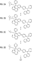
- the Figure 1 shows schematically the structure of an organic semiconductor component 10. This structure is used in particular for organic light-emitting diodes.
- a lower electrode 12 and an upper electrode 13 and a plurality of organic semiconductor layers in between are placed on a glass substrate 11 deposited.
- a cross-section through the horizontally arranged layers is shown.
- the component voltage U d can be applied to the lower 12 and upper 13 electrodes.
- the upper electrode 13 is the cathode of the light-emitting diode and the lower electrode 12 is the anode of the light-emitting diode.
- the light decoupling L occurs through the glass substrate 11.
- the anode is transparent, in particular made of indium tin oxide (ITO).
- the hole-conducting layers 20 initially adjoin the anode. These can be designed for different focus functions.
- the first layer 21 on the anode represents a hole injection layer.
- the hole conductor layer 22 connected to it is a hole transport layer and the third hole conductor layer 23 connected to it functions as an electron blocking layer in order to prevent the electrons coming from the cathode side to penetrate the hole guiding area.
- the electron transport area follows.
- This can also comprise a plurality of electron conducting layers 40.
- the cathode is followed by a first electron conduction layer 43, which acts as an electron injection layer.
- a second electron transport layer 42 is subsequently shown and a third electron transport layer 41 can in turn be used as a hole-blocking layer.
- the emission area is located between the electron transport area and the hole transport area. This in turn can consist of several layers.
- the emission area has three emission layers 30 of different colors: a red emission layer 31 adjoins the hole transport area, followed by a green emission layer 32 and a blue emission layer 33 adjoins the electron transport area.
- the layer according to the invention can also be installed in a charge generation layer.
- the doping can be carried out by coordinating one or two hole conductor molecules, such as, for example, NPB, in the axial positions of the Cu (II) complex, as shown schematically in FIG Figure 2 shown.
- the Figure 2 shows schematically the various representations of the mesomeric boundary structures of the complex:
- the dopant in this example a Cu (II) complex
- NPB hole-conducting matrix
- state B there is a purely formal charge transfer in the form of an electron from the NPB molecule to the Cu (II) complex, ie a formal / partial charge transfer of a positive charge to the NPB molecule.
- the copper atom is then only monovalent.
- state C it is shown that the positive charge, also known as a hole, can move over the NPB molecule and in state D can also be transferred to a second neighboring NPB molecule, which ultimately corresponds to hopping transport in organic semiconductors.
- This coordination can be so strong that even materials that are preferentially electron-conducting in the non-coordinated state are reversed in polarity and become hole conductors.
- Cu (II) trifluoromethanesulfonate can be purified by means of zone sublimation at a base pressure of 2 ⁇ 10 -4 Pa (2 ⁇ 10 -6 mbar).
- the material can in particular be sublimed twice, whereby existing residues and impurities are removed.
- sublimation steps can be carried out at different temperatures.
- HTM-014 a 200 nm thick doped hole conductor layer with the hole conductor matrix material HTM-014 was deposited on an ITO electrode (indium-doped tin oxide) by thermal evaporation.
- the hole conductor is referred to below as HTM-014. This can for example stand for bis-N, N, N ', N' - (naphthyl-phenyl) benzidine.
- a 150 nm thick aluminum layer was deposited as a counter electrode.
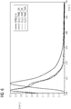
- Figure 3 shows a current-voltage diagram of this organic semiconductor component made of a hole-conducting layer with the Cu (II) TFMS p-doping in different concentrations of 2%, 5% and 10%.
- the component has a base area of 4 mm 2 .
- the doping effect is particularly dependent on the dopant concentration, which is also demonstrated by the example of Cu (II) TFMS in FIG Figure 3 is shown.
- the current density increases with increasing concentration.
- the horizontal areas of the characteristics do not represent a current limitation of the component, but a measurement limit of the measurement setup. The lower the voltage U d at which the maximum measurable current density was measured in the component, the better the doping effect.
- the symmetrical behavior of the current-voltage characteristic for positive and negative operating voltages U d shows that the hole injection is independent of the work function of the electrodes and is therefore the same for the aluminum and ITO electrodes works well.
- the 2% sample does not show a completely symmetrical behavior because the matrix material is a hole transporter.
- the doping concentration of 2% is not yet sufficient to achieve an injection from the aluminum electrode that is comparable to the ITO electrode.
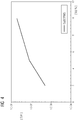
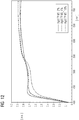
- Figure 4 shows a diagram in which the conductivity of the doped hole transport layer is plotted in Siemens / m as a function of the concentration of the p-dopant in the hole conductor layer.
- substrates on which the conductivity of the doped layers can be measured were coated simultaneously with the samples for the measurement of the current-voltage characteristics.
- differently dimensioned components were produced in order to exclude for the determination of the conductivity that the measured effects depend on the thickness and surface of the components.
- FIG. 4 shows the conductivities as a function of the dopant concentration. The process shown confirms that Figure 3 current-voltage characteristics shown. The conductivity increases the dopant concentration just like the current density.
- the conductivity can only be increased up to material-specific limit values via even higher dopant concentrations, since above a certain concentration it is no longer a matter of doping.
- the Figures 5 , 6th and 7th show the absorption, emission and reflection spectra of the organic hole conductor layers doped with Cu (II) TFMS. For this purpose, these were deposited on quartz glass substrates. These substrates have no electrode contacts and are only used for optical measurements.
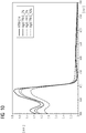
- Figure 6 shows the photoluminescence spectra of the hole conductor layers with the Cu (II) TFMS doping in comparison with the spectrum of undoped HTM-014.
- the emission at a wavelength of 432 nm is shifted to 409 nm by the doping.
- a clear shoulder is formed for the doped layers. Shifting and shouldering can be traced back to the formation of a charge transfer complex.
- Figure 7 shows the reflection spectra of the doped hole conductor layers: with increasing dopant concentration, the reflection falls in the blue-green wavelength range and remains in the red range.
- the layers produced therefore have a red cast to the human eye.
- the dependence on the dopant concentration can also be seen optically: the color of the coated substrates becomes darker and redder to the human eye with increasing concentration.
- silver (I) trifluoromethanesulfonate (Ag (I) TFMS) was used.
- the samples shown were also cleaned up: The zone sublimation at a base pressure of 2 ⁇ 10 -4 Pa (2 ⁇ 10 -6 mbar) took place at 370 ° C.-380 ° C. and produced a yield of 47%.
- the purified Ag (I) TFMS was introduced into the hole conductor matrix HTM-014 for doping.
- the substrates, electrodes, layer thicknesses and component size are identical to the Cu (II) TFMS samples.
- Figure 8 shows a current-voltage diagram of an organic semiconductor component with a hole-conducting layer and p-doping with Ag (I) TFMS in different concentrations.
- concentration By varying the concentration, it can be shown that the doping has an effect on the current-voltage characteristic: At 5% doping concentration, an increase in the current density can be seen for negative as well as for small positive voltages ( ⁇ 2V). The characteristics at 5% and 10% concentration are approximately symmetrical and clearly show the successful doping and the improved electrical conductivity. The symmetrical behavior again shows that the hole injection is independent of the work function of the electrodes. At 10% doping concentration, the characteristic curve again reaches the current limit of the measuring device, as already described.
- Figure 9 shows a diagram in which the conductivity of the hole transport layer in Siemens / m is plotted as a function of the concentration of the p-dopant in the hole conductor layer.
- the samples were produced analogously to the Cu (II) TFMS samples.
- the components with the Ag (I) TFMS-doped hole-conducting layers have the following specific conductivities depending on the doping concentration: 2% Ag (I) TFMS in HTM-014: 2.76 x 10⁻⁵ S / m 5% Ag (I) TFMS in HTM-014: 7.66 x 10 -5 S / m 10% Ag (I) TFMS in HTM-014: 7.86 x 10 -5 S / m
- the Figures 10 , 11 and 12 show the absorption, emission and reflection spectra of the organic hole conductor layers doped with Ag (I) TFMS. For this purpose, these were in turn deposited on quartz glass substrates.
- the absorption spectra in Figure 10 show that the absolute absorption in the absorption maximum at 384 nm wavelength decreases with increasing dopant concentration. At the same time, there is an increase in absorption between 410 nm and 550 nm with increasing dopant concentration. For the visible wavelength range from approx. 400 nm to 700 m, the absorption increases slightly, but in contrast to the Cu (II) TFMS samples, the layers are still color-neutral to the human eye.
- Figure 11 shows the photoluminescence spectra of the hole conductor layers with Ag (I) -TFMS doping. Their comparison with the spectrum of undoped HTM-014 shows that the emission customary from HTM-014 at a wavelength of 432 nm is shifted to 410 nm by the doping. In addition, at 430 nm, a clear shoulder is formed for the doped layers. This shift and shoulder formation is in turn due to the formation of a charge transfer complex.
- Figure 12 shows the reflection spectra of the doped hole conductor layers. With increasing dopant concentration, the reflection in the blue-green wavelength range falls very slightly and remains in the red wavelength range, depending on the dopant concentration. To the human eye, the layers have a neutral color.
Landscapes
- Physics & Mathematics (AREA)
- Engineering & Computer Science (AREA)
- Optics & Photonics (AREA)
- Manufacturing & Machinery (AREA)
- Spectroscopy & Molecular Physics (AREA)
- Chemical & Material Sciences (AREA)
- Materials Engineering (AREA)
- Electroluminescent Light Sources (AREA)
- Photovoltaic Devices (AREA)
Applications Claiming Priority (2)
| Application Number | Priority Date | Filing Date | Title |
|---|---|---|---|
| DE102011003192.8A DE102011003192B4 (de) | 2011-01-26 | 2011-01-26 | Halbleiterbauelement und Verfahren zu seiner Herstellung |
| PCT/EP2012/050117 WO2012100972A1 (de) | 2011-01-26 | 2012-01-05 | Organisches halbleiterbauelement mit dotierter lochleiterschicht |
Publications (2)
| Publication Number | Publication Date |
|---|---|
| EP2656412A1 EP2656412A1 (de) | 2013-10-30 |
| EP2656412B1 true EP2656412B1 (de) | 2020-11-18 |
Family
ID=45446061
Family Applications (1)
| Application Number | Title | Priority Date | Filing Date |
|---|---|---|---|
| EP12700039.6A Active EP2656412B1 (de) | 2011-01-26 | 2012-01-05 | Organisches halbleiterbauelement mit dotierter lochleiterschicht |
Country Status (7)
| Country | Link |
|---|---|
| US (1) | US9263696B2 (ko) |
| EP (1) | EP2656412B1 (ko) |
| JP (1) | JP5869590B2 (ko) |
| KR (1) | KR101991525B1 (ko) |
| CN (1) | CN103339753B (ko) |
| DE (1) | DE102011003192B4 (ko) |
| WO (1) | WO2012100972A1 (ko) |
Families Citing this family (9)
| Publication number | Priority date | Publication date | Assignee | Title |
|---|---|---|---|---|
| DE102011003192B4 (de) | 2011-01-26 | 2015-12-24 | Siemens Aktiengesellschaft | Halbleiterbauelement und Verfahren zu seiner Herstellung |
| DE102013106949A1 (de) * | 2013-07-02 | 2015-01-08 | Osram Opto Semiconductors Gmbh | Optoelektronisches Bauelement, organische funktionelle Schicht und Verfahren zur Herstellung eines optoelektronischen Bauelements |
| DE102013107415A1 (de) * | 2013-07-12 | 2015-01-15 | Osram Opto Semiconductors Gmbh | Organisches lichtemittierendes Bauelement und Verfahren zur Herstellung eines organischen lichtemittierenden Bauelements |
| DE102014210412A1 (de) * | 2014-06-03 | 2015-12-03 | Siemens Aktiengesellschaft | p-Dotierende Vernetzung organischer Lochleiter |
| GB2527606A (en) * | 2014-06-27 | 2015-12-30 | Cambridge Display Tech Ltd | Charge-transfer salt |
| DE102015121844A1 (de) | 2015-12-15 | 2017-06-22 | Osram Oled Gmbh | Organisches elektronisches Bauelement und Verwendung eines fluorierten Sulfonimid-Metallsalzes |
| DE102017111425A1 (de) | 2017-05-24 | 2018-11-29 | Osram Oled Gmbh | Organisches elektronisches Bauelement und Verfahren zur Herstellung eines organischen elektronischen Bauelements |
| DE102018212305A1 (de) | 2018-07-24 | 2020-01-30 | Siemens Aktiengesellschaft | Metallorganische Perowskit-Solarzelle, Tandem-Solarzelle sowie Herstellungsverfahren dazu |
| DE102018212304A1 (de) | 2018-07-24 | 2020-01-30 | Siemens Aktiengesellschaft | Metallorganische Perowskit-Solarzelle, Tandem-Solarzelle sowie Herstellungsverfahren dazu |
Citations (1)
| Publication number | Priority date | Publication date | Assignee | Title |
|---|---|---|---|---|
| WO2006086480A2 (en) * | 2005-02-10 | 2006-08-17 | Plextronics, Inc. | Hole injection/transport layer compositions and devices |
Family Cites Families (21)
| Publication number | Priority date | Publication date | Assignee | Title |
|---|---|---|---|---|
| US5853906A (en) * | 1997-10-14 | 1998-12-29 | Xerox Corporation | Conductive polymer compositions and processes thereof |
| JPH11251067A (ja) | 1998-03-02 | 1999-09-17 | Junji Kido | 有機エレクトロルミネッセント素子 |
| WO2003065770A1 (fr) | 2002-01-31 | 2003-08-07 | Sumitomo Chemical Company, Limited | Dispositif d'electroluminescence organique |
| JP4363050B2 (ja) | 2002-01-31 | 2009-11-11 | 住友化学株式会社 | 有機エレクトロルミネッセンス素子 |
| JP2003272865A (ja) | 2002-03-19 | 2003-09-26 | Mitsubishi Rayon Co Ltd | 有機電界発光素子 |
| US7390438B2 (en) * | 2003-04-22 | 2008-06-24 | E.I. Du Pont De Nemours And Company | Water dispersible substituted polydioxythiophenes made with fluorinated polymeric sulfonic acid colloids |
| GB0311234D0 (en) | 2003-05-16 | 2003-06-18 | Isis Innovation | Organic phosphorescent material and organic optoelectronic device |
| US7455793B2 (en) | 2004-03-31 | 2008-11-25 | E.I. Du Pont De Nemours And Company | Non-aqueous dispersions comprising electrically doped conductive polymers and colloid-forming polymeric acids |
| US20060008671A1 (en) | 2004-07-07 | 2006-01-12 | Raymond Kwong | Electroluminescent efficiency |
| US7851072B2 (en) | 2005-05-19 | 2010-12-14 | Universal Display Corporation | Stable and efficient electroluminescent materials |
| JP5323478B2 (ja) | 2005-06-27 | 2013-10-23 | イー・アイ・デュポン・ドウ・ヌムール・アンド・カンパニー | 導電性ポリマー組成物 |
| WO2008057615A2 (en) * | 2006-03-03 | 2008-05-15 | Eikos, Inc. | Highly transparent and conductive carbon nanotube coatings |
| DE102007028238A1 (de) * | 2007-06-20 | 2008-12-24 | Osram Opto Semiconductors Gmbh | Verwendung eines Metallkomplexes als p-Dotand für ein organisches halbleitendes Matrixmaterial, organisches Halbleitermaterial und organische Leuchtdiode |
| KR101435999B1 (ko) * | 2007-12-07 | 2014-08-29 | 삼성전자주식회사 | 도펀트로 도핑된 산화그라펜의 환원물, 이를 포함하는 박막및 투명전극 |
| KR20090092114A (ko) * | 2008-02-26 | 2009-08-31 | 삼성모바일디스플레이주식회사 | 초강산의 염을 포함하는 전자 주입층, 이를 포함하는광전변환 소자 및 이를 포함하는 유기 발광 소자 |
| JP5104428B2 (ja) | 2008-03-13 | 2012-12-19 | コニカミノルタホールディングス株式会社 | 有機半導体材料、これを用いた電界効果トランジスタ |
| EP2350216B1 (en) | 2008-10-27 | 2021-03-03 | Nissan Chemical Corporation | Charge injection and transport layers |
| JP2010265236A (ja) | 2009-05-18 | 2010-11-25 | Sumitomo Chemical Co Ltd | 含シリルチアゾリウムヨーダイド又は含シリルオキサゾリウムヨーダイド及びその用途 |
| US8580394B2 (en) * | 2009-11-19 | 2013-11-12 | Universal Display Corporation | 3-coordinate copper(I)-carbene complexes |
| DE102010056519A1 (de) * | 2010-12-27 | 2012-06-28 | Heliatek Gmbh | Optoelektronisches Bauelement mit dotierten Schichten |
| DE102011003192B4 (de) | 2011-01-26 | 2015-12-24 | Siemens Aktiengesellschaft | Halbleiterbauelement und Verfahren zu seiner Herstellung |
-
2011
- 2011-01-26 DE DE102011003192.8A patent/DE102011003192B4/de active Active
-
2012
- 2012-01-05 WO PCT/EP2012/050117 patent/WO2012100972A1/de active Application Filing
- 2012-01-05 KR KR1020137022295A patent/KR101991525B1/ko active IP Right Grant
- 2012-01-05 CN CN201280006603.1A patent/CN103339753B/zh active Active
- 2012-01-05 EP EP12700039.6A patent/EP2656412B1/de active Active
- 2012-01-05 US US13/982,053 patent/US9263696B2/en active Active
- 2012-01-05 JP JP2013550813A patent/JP5869590B2/ja active Active
Patent Citations (1)
| Publication number | Priority date | Publication date | Assignee | Title |
|---|---|---|---|---|
| WO2006086480A2 (en) * | 2005-02-10 | 2006-08-17 | Plextronics, Inc. | Hole injection/transport layer compositions and devices |
Non-Patent Citations (1)
| Title |
|---|
| AGNES KÜTT ET AL: "Equilibrium Acidities of Superacids", JOURNAL OF ORGANIC CHEMISTRY, vol. 76, no. 2, 17 December 2010 (2010-12-17), US, pages 391 - 395, XP055235130, ISSN: 0022-3263, DOI: 10.1021/jo101409p * |
Also Published As
| Publication number | Publication date |
|---|---|
| JP2014511021A (ja) | 2014-05-01 |
| CN103339753B (zh) | 2016-11-09 |
| DE102011003192B4 (de) | 2015-12-24 |
| US9263696B2 (en) | 2016-02-16 |
| US20140034934A1 (en) | 2014-02-06 |
| EP2656412A1 (de) | 2013-10-30 |
| JP5869590B2 (ja) | 2016-02-24 |
| WO2012100972A1 (de) | 2012-08-02 |
| KR101991525B1 (ko) | 2019-06-20 |
| CN103339753A (zh) | 2013-10-02 |
| DE102011003192A1 (de) | 2012-07-26 |
| KR20140007395A (ko) | 2014-01-17 |
Similar Documents
| Publication | Publication Date | Title |
|---|---|---|
| EP2656412B1 (de) | Organisches halbleiterbauelement mit dotierter lochleiterschicht | |
| EP2553047B1 (de) | Dotierstoff für eine lochleiterschicht für organische halbleiterbauelemente und verwendung dazu | |
| DE102012101652B4 (de) | Organisches halbleitendes Material und elektronisches Bauelement | |
| EP3246960B1 (de) | Hauptgruppenmetallkomplexe als p-dotanden für organische elektronische matrixmaterialien | |
| EP1656706B1 (de) | Organisches elektrolumineszenzelement | |
| DE60306570T2 (de) | Organische elektrolumineszente Vorrichtungen | |
| DE102008051737B4 (de) | Quadratisch planare Übergangsmetallkomplexe, organische halbleitende Materialien sowie elektronische oder optoelektronische Bauelemente, die diese umfassen und Verwendung derselben | |
| EP1806795B1 (de) | Organisches Bauelement | |
| DE102007018456B4 (de) | Verwendung von Hauptgruppenelementhalogeniden und/oder -pseudohalogeniden, organisches halbleitendes Matrixmaterial, elektronische und optoelektronische Bauelemente | |
| DE112008004292B3 (de) | Licht emittierendes Bauelement und Verfahren zum Herstellen | |
| EP2691997B1 (de) | Komplexierung niedermolekularer halbleiter für die anwendung als emitterkomplex in organischen lichtemittierenden elektrochemischen zellen (oleecs) | |
| EP2483945B1 (de) | Organische elektronische vorrichtung und verfahren zu deren herstellung | |
| EP2158625B1 (de) | Verwendung eines metallkomplexes als p-dotand für ein organisches halbleitendes matrixmaterial, organisches halbleitermaterial und organische leuchtdioden | |
| WO2005036667A1 (de) | N- dotierung von organischen halbleitern | |
| EP1786050A1 (de) | Dotiertes organisches Halbleitermaterial | |
| EP1668718B1 (de) | Organisches elektrolumineszenzelement | |
| WO2008058525A2 (de) | Verwendung einer koordinationsverbindung zur dotierung von organischen halbleitern | |
| WO2011134458A1 (de) | Organisches halbleitendes material und elektronisches bauelement | |
| WO2013057130A1 (de) | Organisches elektronisches bauelement mit dotierstoff, verwendung eines dotierstoffs und verfahren zur herstellung des dotierstoffs | |
| EP3201959B1 (de) | Organisches elektronisches bauteil | |
| EP2483943B1 (de) | Optoelektronisches organisches bauelement und verfahren zu dessen herstellung | |
| EP1643568A1 (de) | Verfahren zum Herstellen einer Schicht aus einem dotierten Halbleitermaterial und Vorrichtung | |
| WO2017178473A1 (de) | Organisches elektronisches bauteil mit ladungsträger-generationsschicht | |
| WO2010057471A1 (de) | Chinoxalinverbindungen und halbleitermaterialien | |
| DE102018212304A1 (de) | Metallorganische Perowskit-Solarzelle, Tandem-Solarzelle sowie Herstellungsverfahren dazu |
Legal Events
| Date | Code | Title | Description |
|---|---|---|---|
| PUAI | Public reference made under article 153(3) epc to a published international application that has entered the european phase |
Free format text: ORIGINAL CODE: 0009012 |
|
| 17P | Request for examination filed |
Effective date: 20130614 |
|
| AK | Designated contracting states |
Kind code of ref document: A1 Designated state(s): AL AT BE BG CH CY CZ DE DK EE ES FI FR GB GR HR HU IE IS IT LI LT LU LV MC MK MT NL NO PL PT RO RS SE SI SK SM TR |
|
| RIN1 | Information on inventor provided before grant (corrected) |
Inventor name: KELLERMANN, RENATE Inventor name: SCHMID, GUENTER Inventor name: MALTENBERGER, ANNA Inventor name: WEMKEN, JAN HAUKE |
|
| DAX | Request for extension of the european patent (deleted) | ||
| RAP1 | Party data changed (applicant data changed or rights of an application transferred) |
Owner name: SIEMENS AKTIENGESELLSCHAFT |
|
| STAA | Information on the status of an ep patent application or granted ep patent |
Free format text: STATUS: EXAMINATION IS IN PROGRESS |
|
| 17Q | First examination report despatched |
Effective date: 20190719 |
|
| GRAP | Despatch of communication of intention to grant a patent |
Free format text: ORIGINAL CODE: EPIDOSNIGR1 |
|
| STAA | Information on the status of an ep patent application or granted ep patent |
Free format text: STATUS: GRANT OF PATENT IS INTENDED |
|
| INTG | Intention to grant announced |
Effective date: 20200316 |
|
| GRAS | Grant fee paid |
Free format text: ORIGINAL CODE: EPIDOSNIGR3 |
|
| GRAA | (expected) grant |
Free format text: ORIGINAL CODE: 0009210 |
|
| STAA | Information on the status of an ep patent application or granted ep patent |
Free format text: STATUS: THE PATENT HAS BEEN GRANTED |
|
| AK | Designated contracting states |
Kind code of ref document: B1 Designated state(s): AL AT BE BG CH CY CZ DE DK EE ES FI FR GB GR HR HU IE IS IT LI LT LU LV MC MK MT NL NO PL PT RO RS SE SI SK SM TR |
|
| RAP1 | Party data changed (applicant data changed or rights of an application transferred) |
Owner name: NOVALED GMBH |
|
| REG | Reference to a national code |
Ref country code: GB Ref legal event code: FG4D Free format text: NOT ENGLISH |
|
| REG | Reference to a national code |
Ref country code: CH Ref legal event code: EP |
|
| REG | Reference to a national code |
Ref country code: IE Ref legal event code: FG4D Free format text: LANGUAGE OF EP DOCUMENT: GERMAN |
|
| REG | Reference to a national code |
Ref country code: DE Ref legal event code: R096 Ref document number: 502012016482 Country of ref document: DE |
|
| REG | Reference to a national code |
Ref country code: AT Ref legal event code: REF Ref document number: 1336739 Country of ref document: AT Kind code of ref document: T Effective date: 20201215 |
|
| REG | Reference to a national code |
Ref country code: NL Ref legal event code: MP Effective date: 20201118 |
|
| PG25 | Lapsed in a contracting state [announced via postgrant information from national office to epo] |
Ref country code: RS Free format text: LAPSE BECAUSE OF FAILURE TO SUBMIT A TRANSLATION OF THE DESCRIPTION OR TO PAY THE FEE WITHIN THE PRESCRIBED TIME-LIMIT Effective date: 20201118 Ref country code: FI Free format text: LAPSE BECAUSE OF FAILURE TO SUBMIT A TRANSLATION OF THE DESCRIPTION OR TO PAY THE FEE WITHIN THE PRESCRIBED TIME-LIMIT Effective date: 20201118 Ref country code: NO Free format text: LAPSE BECAUSE OF FAILURE TO SUBMIT A TRANSLATION OF THE DESCRIPTION OR TO PAY THE FEE WITHIN THE PRESCRIBED TIME-LIMIT Effective date: 20210218 Ref country code: PT Free format text: LAPSE BECAUSE OF FAILURE TO SUBMIT A TRANSLATION OF THE DESCRIPTION OR TO PAY THE FEE WITHIN THE PRESCRIBED TIME-LIMIT Effective date: 20210318 Ref country code: GR Free format text: LAPSE BECAUSE OF FAILURE TO SUBMIT A TRANSLATION OF THE DESCRIPTION OR TO PAY THE FEE WITHIN THE PRESCRIBED TIME-LIMIT Effective date: 20210219 |
|
| PG25 | Lapsed in a contracting state [announced via postgrant information from national office to epo] |
Ref country code: SE Free format text: LAPSE BECAUSE OF FAILURE TO SUBMIT A TRANSLATION OF THE DESCRIPTION OR TO PAY THE FEE WITHIN THE PRESCRIBED TIME-LIMIT Effective date: 20201118 Ref country code: PL Free format text: LAPSE BECAUSE OF FAILURE TO SUBMIT A TRANSLATION OF THE DESCRIPTION OR TO PAY THE FEE WITHIN THE PRESCRIBED TIME-LIMIT Effective date: 20201118 Ref country code: IS Free format text: LAPSE BECAUSE OF FAILURE TO SUBMIT A TRANSLATION OF THE DESCRIPTION OR TO PAY THE FEE WITHIN THE PRESCRIBED TIME-LIMIT Effective date: 20210318 Ref country code: LV Free format text: LAPSE BECAUSE OF FAILURE TO SUBMIT A TRANSLATION OF THE DESCRIPTION OR TO PAY THE FEE WITHIN THE PRESCRIBED TIME-LIMIT Effective date: 20201118 Ref country code: BG Free format text: LAPSE BECAUSE OF FAILURE TO SUBMIT A TRANSLATION OF THE DESCRIPTION OR TO PAY THE FEE WITHIN THE PRESCRIBED TIME-LIMIT Effective date: 20210218 |
|
| REG | Reference to a national code |
Ref country code: LT Ref legal event code: MG9D |
|
| PG25 | Lapsed in a contracting state [announced via postgrant information from national office to epo] |
Ref country code: HR Free format text: LAPSE BECAUSE OF FAILURE TO SUBMIT A TRANSLATION OF THE DESCRIPTION OR TO PAY THE FEE WITHIN THE PRESCRIBED TIME-LIMIT Effective date: 20201118 |
|
| PG25 | Lapsed in a contracting state [announced via postgrant information from national office to epo] |
Ref country code: SK Free format text: LAPSE BECAUSE OF FAILURE TO SUBMIT A TRANSLATION OF THE DESCRIPTION OR TO PAY THE FEE WITHIN THE PRESCRIBED TIME-LIMIT Effective date: 20201118 Ref country code: RO Free format text: LAPSE BECAUSE OF FAILURE TO SUBMIT A TRANSLATION OF THE DESCRIPTION OR TO PAY THE FEE WITHIN THE PRESCRIBED TIME-LIMIT Effective date: 20201118 Ref country code: LT Free format text: LAPSE BECAUSE OF FAILURE TO SUBMIT A TRANSLATION OF THE DESCRIPTION OR TO PAY THE FEE WITHIN THE PRESCRIBED TIME-LIMIT Effective date: 20201118 Ref country code: SM Free format text: LAPSE BECAUSE OF FAILURE TO SUBMIT A TRANSLATION OF THE DESCRIPTION OR TO PAY THE FEE WITHIN THE PRESCRIBED TIME-LIMIT Effective date: 20201118 Ref country code: EE Free format text: LAPSE BECAUSE OF FAILURE TO SUBMIT A TRANSLATION OF THE DESCRIPTION OR TO PAY THE FEE WITHIN THE PRESCRIBED TIME-LIMIT Effective date: 20201118 Ref country code: CZ Free format text: LAPSE BECAUSE OF FAILURE TO SUBMIT A TRANSLATION OF THE DESCRIPTION OR TO PAY THE FEE WITHIN THE PRESCRIBED TIME-LIMIT Effective date: 20201118 |
|
| REG | Reference to a national code |
Ref country code: DE Ref legal event code: R097 Ref document number: 502012016482 Country of ref document: DE |
|
| PG25 | Lapsed in a contracting state [announced via postgrant information from national office to epo] |
Ref country code: DK Free format text: LAPSE BECAUSE OF FAILURE TO SUBMIT A TRANSLATION OF THE DESCRIPTION OR TO PAY THE FEE WITHIN THE PRESCRIBED TIME-LIMIT Effective date: 20201118 Ref country code: MC Free format text: LAPSE BECAUSE OF FAILURE TO SUBMIT A TRANSLATION OF THE DESCRIPTION OR TO PAY THE FEE WITHIN THE PRESCRIBED TIME-LIMIT Effective date: 20201118 |
|
| REG | Reference to a national code |
Ref country code: CH Ref legal event code: PL |
|
| PLBE | No opposition filed within time limit |
Free format text: ORIGINAL CODE: 0009261 |
|
| STAA | Information on the status of an ep patent application or granted ep patent |
Free format text: STATUS: NO OPPOSITION FILED WITHIN TIME LIMIT |
|
| PG25 | Lapsed in a contracting state [announced via postgrant information from national office to epo] |
Ref country code: LU Free format text: LAPSE BECAUSE OF NON-PAYMENT OF DUE FEES Effective date: 20210105 |
|
| REG | Reference to a national code |
Ref country code: BE Ref legal event code: MM Effective date: 20210131 |
|
| 26N | No opposition filed |
Effective date: 20210819 |
|
| GBPC | Gb: european patent ceased through non-payment of renewal fee |
Effective date: 20210218 |
|
| PG25 | Lapsed in a contracting state [announced via postgrant information from national office to epo] |
Ref country code: FR Free format text: LAPSE BECAUSE OF NON-PAYMENT OF DUE FEES Effective date: 20210118 Ref country code: NL Free format text: LAPSE BECAUSE OF FAILURE TO SUBMIT A TRANSLATION OF THE DESCRIPTION OR TO PAY THE FEE WITHIN THE PRESCRIBED TIME-LIMIT Effective date: 20201118 Ref country code: IT Free format text: LAPSE BECAUSE OF FAILURE TO SUBMIT A TRANSLATION OF THE DESCRIPTION OR TO PAY THE FEE WITHIN THE PRESCRIBED TIME-LIMIT Effective date: 20201118 Ref country code: AL Free format text: LAPSE BECAUSE OF FAILURE TO SUBMIT A TRANSLATION OF THE DESCRIPTION OR TO PAY THE FEE WITHIN THE PRESCRIBED TIME-LIMIT Effective date: 20201118 |
|
| PG25 | Lapsed in a contracting state [announced via postgrant information from national office to epo] |
Ref country code: SI Free format text: LAPSE BECAUSE OF FAILURE TO SUBMIT A TRANSLATION OF THE DESCRIPTION OR TO PAY THE FEE WITHIN THE PRESCRIBED TIME-LIMIT Effective date: 20201118 Ref country code: LI Free format text: LAPSE BECAUSE OF NON-PAYMENT OF DUE FEES Effective date: 20210131 Ref country code: ES Free format text: LAPSE BECAUSE OF FAILURE TO SUBMIT A TRANSLATION OF THE DESCRIPTION OR TO PAY THE FEE WITHIN THE PRESCRIBED TIME-LIMIT Effective date: 20201118 Ref country code: CH Free format text: LAPSE BECAUSE OF NON-PAYMENT OF DUE FEES Effective date: 20210131 |
|
| PG25 | Lapsed in a contracting state [announced via postgrant information from national office to epo] |
Ref country code: IE Free format text: LAPSE BECAUSE OF NON-PAYMENT OF DUE FEES Effective date: 20210105 Ref country code: GB Free format text: LAPSE BECAUSE OF NON-PAYMENT OF DUE FEES Effective date: 20210218 |
|
| REG | Reference to a national code |
Ref country code: AT Ref legal event code: MM01 Ref document number: 1336739 Country of ref document: AT Kind code of ref document: T Effective date: 20210105 |
|
| PG25 | Lapsed in a contracting state [announced via postgrant information from national office to epo] |
Ref country code: AT Free format text: LAPSE BECAUSE OF NON-PAYMENT OF DUE FEES Effective date: 20210105 |
|
| PG25 | Lapsed in a contracting state [announced via postgrant information from national office to epo] |
Ref country code: IS Free format text: LAPSE BECAUSE OF FAILURE TO SUBMIT A TRANSLATION OF THE DESCRIPTION OR TO PAY THE FEE WITHIN THE PRESCRIBED TIME-LIMIT Effective date: 20210318 |
|
| PG25 | Lapsed in a contracting state [announced via postgrant information from national office to epo] |
Ref country code: BE Free format text: LAPSE BECAUSE OF NON-PAYMENT OF DUE FEES Effective date: 20210131 |
|
| REG | Reference to a national code |
Ref country code: DE Ref legal event code: R079 Ref document number: 502012016482 Country of ref document: DE Free format text: PREVIOUS MAIN CLASS: H01L0051000000 Ipc: H10K0099000000 |
|
| PG25 | Lapsed in a contracting state [announced via postgrant information from national office to epo] |
Ref country code: HU Free format text: LAPSE BECAUSE OF FAILURE TO SUBMIT A TRANSLATION OF THE DESCRIPTION OR TO PAY THE FEE WITHIN THE PRESCRIBED TIME-LIMIT; INVALID AB INITIO Effective date: 20120105 Ref country code: CY Free format text: LAPSE BECAUSE OF FAILURE TO SUBMIT A TRANSLATION OF THE DESCRIPTION OR TO PAY THE FEE WITHIN THE PRESCRIBED TIME-LIMIT Effective date: 20201118 |
|
| P01 | Opt-out of the competence of the unified patent court (upc) registered |
Effective date: 20230526 |
|
| PG25 | Lapsed in a contracting state [announced via postgrant information from national office to epo] |
Ref country code: MK Free format text: LAPSE BECAUSE OF FAILURE TO SUBMIT A TRANSLATION OF THE DESCRIPTION OR TO PAY THE FEE WITHIN THE PRESCRIBED TIME-LIMIT Effective date: 20201118 |
|
| PGFP | Annual fee paid to national office [announced via postgrant information from national office to epo] |
Ref country code: DE Payment date: 20231128 Year of fee payment: 13 |