EP2652789B1 - Memory device comprising a strained semiconductor double-heterostructure and quantum dots - Google Patents
Memory device comprising a strained semiconductor double-heterostructure and quantum dots Download PDFInfo
- Publication number
- EP2652789B1 EP2652789B1 EP11807878.1A EP11807878A EP2652789B1 EP 2652789 B1 EP2652789 B1 EP 2652789B1 EP 11807878 A EP11807878 A EP 11807878A EP 2652789 B1 EP2652789 B1 EP 2652789B1
- Authority
- EP
- European Patent Office
- Prior art keywords
- heterostructure
- memory
- energy
- gate electrode
- layer
- Prior art date
- Legal status (The legal status is an assumption and is not a legal conclusion. Google has not performed a legal analysis and makes no representation as to the accuracy of the status listed.)
- Active
Links
- 239000002096 quantum dot Substances 0.000 title claims description 69
- 239000004065 semiconductor Substances 0.000 title claims description 36
- 230000015654 memory Effects 0.000 claims description 39
- 230000004888 barrier function Effects 0.000 claims description 18
- 230000005669 field effect Effects 0.000 claims description 13
- 239000004047 hole gas Substances 0.000 claims description 12
- 239000002800 charge carrier Substances 0.000 claims description 8
- 239000003362 semiconductor superlattice Substances 0.000 claims description 8
- 230000005641 tunneling Effects 0.000 claims description 8
- 238000007599 discharging Methods 0.000 claims description 6
- 230000015572 biosynthetic process Effects 0.000 claims description 2
- 230000004044 response Effects 0.000 claims 2
- 230000001939 inductive effect Effects 0.000 claims 1
- 229910001218 Gallium arsenide Inorganic materials 0.000 description 10
- 229910000673 Indium arsenide Inorganic materials 0.000 description 6
- RPQDHPTXJYYUPQ-UHFFFAOYSA-N indium arsenide Chemical compound [In]#[As] RPQDHPTXJYYUPQ-UHFFFAOYSA-N 0.000 description 6
- 238000000034 method Methods 0.000 description 6
- 230000005684 electric field Effects 0.000 description 5
- 230000004807 localization Effects 0.000 description 5
- 238000005259 measurement Methods 0.000 description 5
- 230000008569 process Effects 0.000 description 5
- 230000007423 decrease Effects 0.000 description 4
- 239000000969 carrier Substances 0.000 description 3
- 230000005283 ground state Effects 0.000 description 3
- 239000000463 material Substances 0.000 description 3
- VYPSYNLAJGMNEJ-UHFFFAOYSA-N Silicium dioxide Chemical compound O=[Si]=O VYPSYNLAJGMNEJ-UHFFFAOYSA-N 0.000 description 2
- 238000005452 bending Methods 0.000 description 2
- 230000003247 decreasing effect Effects 0.000 description 2
- 230000000694 effects Effects 0.000 description 2
- 230000006870 function Effects 0.000 description 2
- 230000003446 memory effect Effects 0.000 description 2
- 230000003071 parasitic effect Effects 0.000 description 2
- 230000009467 reduction Effects 0.000 description 2
- 239000000758 substrate Substances 0.000 description 2
- 230000001052 transient effect Effects 0.000 description 2
- 229910000980 Aluminium gallium arsenide Inorganic materials 0.000 description 1
- 229910001020 Au alloy Inorganic materials 0.000 description 1
- 229910005542 GaSb Inorganic materials 0.000 description 1
- 229910001297 Zn alloy Inorganic materials 0.000 description 1
- 238000013459 approach Methods 0.000 description 1
- 230000008859 change Effects 0.000 description 1
- 229910052681 coesite Inorganic materials 0.000 description 1
- 230000002596 correlated effect Effects 0.000 description 1
- 229910052906 cristobalite Inorganic materials 0.000 description 1
- 238000001773 deep-level transient spectroscopy Methods 0.000 description 1
- 230000007547 defect Effects 0.000 description 1
- 230000008034 disappearance Effects 0.000 description 1
- 238000011835 investigation Methods 0.000 description 1
- 238000012544 monitoring process Methods 0.000 description 1
- 230000006798 recombination Effects 0.000 description 1
- 238000005215 recombination Methods 0.000 description 1
- 239000000377 silicon dioxide Substances 0.000 description 1
- 125000006850 spacer group Chemical group 0.000 description 1
- 230000003068 static effect Effects 0.000 description 1
- 229910052682 stishovite Inorganic materials 0.000 description 1
- 239000000126 substance Substances 0.000 description 1
- 238000012546 transfer Methods 0.000 description 1
- 229910052905 tridymite Inorganic materials 0.000 description 1
- 238000001039 wet etching Methods 0.000 description 1
Images


Classifications
-
- H—ELECTRICITY
- H10—SEMICONDUCTOR DEVICES; ELECTRIC SOLID-STATE DEVICES NOT OTHERWISE PROVIDED FOR
- H10D—INORGANIC ELECTRIC SEMICONDUCTOR DEVICES
- H10D62/00—Semiconductor bodies, or regions thereof, of devices having potential barriers
- H10D62/80—Semiconductor bodies, or regions thereof, of devices having potential barriers characterised by the materials
- H10D62/81—Semiconductor bodies, or regions thereof, of devices having potential barriers characterised by the materials of structures exhibiting quantum-confinement effects, e.g. single quantum wells; of structures having periodic or quasi-periodic potential variation
-
- B—PERFORMING OPERATIONS; TRANSPORTING
- B82—NANOTECHNOLOGY
- B82Y—SPECIFIC USES OR APPLICATIONS OF NANOSTRUCTURES; MEASUREMENT OR ANALYSIS OF NANOSTRUCTURES; MANUFACTURE OR TREATMENT OF NANOSTRUCTURES
- B82Y10/00—Nanotechnology for information processing, storage or transmission, e.g. quantum computing or single electron logic
-
- H—ELECTRICITY
- H10—SEMICONDUCTOR DEVICES; ELECTRIC SOLID-STATE DEVICES NOT OTHERWISE PROVIDED FOR
- H10D—INORGANIC ELECTRIC SEMICONDUCTOR DEVICES
- H10D30/00—Field-effect transistors [FET]
- H10D30/40—FETs having zero-dimensional [0D], one-dimensional [1D] or two-dimensional [2D] charge carrier gas channels
- H10D30/47—FETs having zero-dimensional [0D], one-dimensional [1D] or two-dimensional [2D] charge carrier gas channels having 2D charge carrier gas channels, e.g. nanoribbon FETs or high electron mobility transistors [HEMT]
-
- H—ELECTRICITY
- H10—SEMICONDUCTOR DEVICES; ELECTRIC SOLID-STATE DEVICES NOT OTHERWISE PROVIDED FOR
- H10D—INORGANIC ELECTRIC SEMICONDUCTOR DEVICES
- H10D30/00—Field-effect transistors [FET]
- H10D30/80—FETs having rectifying junction gate electrodes
- H10D30/801—FETs having heterojunction gate electrodes
- H10D30/803—Programmable transistors, e.g. having charge-trapping quantum well
-
- H—ELECTRICITY
- H10—SEMICONDUCTOR DEVICES; ELECTRIC SOLID-STATE DEVICES NOT OTHERWISE PROVIDED FOR
- H10D—INORGANIC ELECTRIC SEMICONDUCTOR DEVICES
- H10D48/00—Individual devices not covered by groups H10D1/00 - H10D44/00
- H10D48/30—Devices controlled by electric currents or voltages
-
- H—ELECTRICITY
- H10—SEMICONDUCTOR DEVICES; ELECTRIC SOLID-STATE DEVICES NOT OTHERWISE PROVIDED FOR
- H10D—INORGANIC ELECTRIC SEMICONDUCTOR DEVICES
- H10D48/00—Individual devices not covered by groups H10D1/00 - H10D44/00
- H10D48/30—Devices controlled by electric currents or voltages
- H10D48/32—Devices controlled by only the electric current supplied, or only the electric potential applied, to an electrode which does not carry the current to be rectified, amplified or switched
-
- H—ELECTRICITY
- H10—SEMICONDUCTOR DEVICES; ELECTRIC SOLID-STATE DEVICES NOT OTHERWISE PROVIDED FOR
- H10D—INORGANIC ELECTRIC SEMICONDUCTOR DEVICES
- H10D30/00—Field-effect transistors [FET]
- H10D30/01—Manufacture or treatment
- H10D30/021—Manufacture or treatment of FETs having insulated gates [IGFET]
- H10D30/0411—Manufacture or treatment of FETs having insulated gates [IGFET] of FETs having floating gates
-
- H—ELECTRICITY
- H10—SEMICONDUCTOR DEVICES; ELECTRIC SOLID-STATE DEVICES NOT OTHERWISE PROVIDED FOR
- H10D—INORGANIC ELECTRIC SEMICONDUCTOR DEVICES
- H10D30/00—Field-effect transistors [FET]
- H10D30/60—Insulated-gate field-effect transistors [IGFET]
- H10D30/68—Floating-gate IGFETs
Definitions
- the gate electrode of the field effect transistor may be a Schottky contact.
- the quantum dots in the inner semiconductor layer may be arranged in an array.
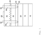
- the exemplary embodiment of Figure 1 consists of a quantumwell modulation doped field-effect transistor with a single InAs/GaAs QD layer in close vicinity to the 2DHG.
- a schematic cross section of the layer structure is shown in Figure 1 .
- a 1 ⁇ m thick undoped GaAs buffer layer 10 was grown first on an undoped GaAs substrate 15.
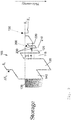
- Figure 2 schematically shows the valence band of the structure for the three memory operations: storage, writing, and erasing.
- the binding potential of holes in the QDs represents the emission barrier, needed to store a logical "1".
- a capture barrier is necessary, which is formed by the band-bending of the Schottky contact.
- the charged QDs act as Coulomb scattering centers, reducing the mobility of the 2DHG.
- Gauss' law it was predicted that the transfer of holes in QDs lead to a reduction in the carrier density in the 2DHG.
- Both the lowered charge carrier density and the decreased mobility reduce the conductance during the down sweep, resulting in a lower current trace compared to the up sweep.
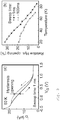
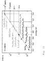
- the maximum hysteresis opening with respect to the up sweep is shown in Fig. 3(b) as a function of temperature for two different sweep times. Using a sweep time of 1 ms, the hysteresis opening drops from 32% at 20 K to almost zero at 85 K. The descent has its origin in the reduced charge carrier storage time of QDs with increasing temperature, i.e., at higher temperatures more holes are emitted during the down sweep.
- Figure 4 shows the transients at 50 K for three different storage voltages (0, 0.4, and 0.7 V).
- the upper transients represent hole capture into initially empty QDs, leading to a decrease in the conductance of the 2DHG and, hence, to a decrease in the drain current.
- the lower transients represent hole emission out of fully occupied QDs and, thus, the drain current increases to the equilibrium state.
- a change of the storage voltage from 0 to 0.4 V and further to 0.7 V causes multiple effects ( Figs. 4(a)-4(c) ); the time constants of both transients increase, the amplitude of the capture transient is reduced, and the amplitude of the emission transient is increased.
- Figs. 4(a)-4(c) the valence band profiles for the three storage voltages are shown.
- the amplitudes of the transients represent the amount of transferred holes and are correlated with the number of levels which are below the Fermi level (for capture) and above the Fermi level (for emission).
- a larger positive storage voltage shifts the Fermi level toward the QD ground state and, hence, more holes are emitted, less holes are captured, and thus the amplitudes vary.
- This saturation has presently its origin in a parasitic cut-off frequency of about 2 MHz of the RC low pass of our present devices. Much faster write times are expected for smaller devices having larger parasitic cut-off frequencies.
- the erase times are shown in Fig. 5(b) .
- a minimum erase time of 350 ns at 50 K was obtained for an erase pulse of 2.5 V.
- the temperature dependence of the write and erase times reflects again the increased thermal capture and emission rates at higher temperatures.
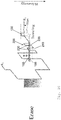
- Figure 6 shows a memory 105 comprising a strained double-heterostructure 110 having an inner semiconductor layer 115 which may consist of Ga(As,Sb) and which is sandwiched between two outer semiconductor layers 120 and 125.
- the outer semiconductor layers 120 and 125 may consist of (Al,Ga)As.
- the at least one quantum dot Due to the lattice strain, the at least one quantum dot has an emission barrier Eb of 1,15 eV or higher, and provides an energy state density of at least three energy states per 1000 nm 3 . All of the at least three energy states are located in an energy band ⁇ Wb of 50 meV or less. The energy band ⁇ Wb is provided such that each of said at least three energy states is capable of storing two holes.
- the memory of Figure 6 further comprises an intermediate layer 140 which is arranged between the gate electrode 135 of the field effect transistor and the strained double-heterostructure 110.
- the intermediate layer 140 has a smaller band gap than the adjacent outer semiconductor layer 120 of the strained double-heterostructure 110.
- the smaller band gap provides a conduction band discontinuity ⁇ E L at the interface between the intermediate layer 140 and the adjacent outer semiconductor layer 120.
- the conduction band discontinuity ⁇ E L prevents electrons originating from gate 135 to get into the outer semiconductor layer 120 if a positive bias voltage is applied.
- the conduction band discontinuity ⁇ E L avoids recombination of electrons and holes in the inner semiconductor layer 115.
- the gate contact of the field effect transistor is preferably an ohmic contact, and the intermediate layer 140 is preferably n-doped.
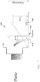
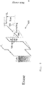
- Figure 8 shows the memory 105 after applying an erase-voltage to the strained double-heterostructure. It can be seen that the holes 185 stored in the energy states of the quantum dot may tunnel through the energy barrier 190 and reach the 2-dimensional hole gas layer 130.
- the third embodiment comprises a semiconductor superlattice 200 which is arranged between the 2-dimensional hole gas layer 130 and the outer semiconductor layer 125.
- the semiconductor superlattice 200 comprises two quantum wells 210 and 220. Each quantum well 210 and 220 provides at least one energy state 230.
- the erase process is based on hole tunneling through the entire emission barrier.
- the erase time depends on the height of the emission barrier.
- an emission barrier of 1.15 eV or higher high electric fields in the range of MV/cm are needed to reach fast erase times [11]. This high electric fields lead to a high power consumption of the memory cell and to a low endurance, as defects in the lattice could be generated.
Landscapes
- Engineering & Computer Science (AREA)
- Chemical & Material Sciences (AREA)
- Nanotechnology (AREA)
- Physics & Mathematics (AREA)
- Mathematical Physics (AREA)
- Theoretical Computer Science (AREA)
- Crystallography & Structural Chemistry (AREA)
- Semiconductor Memories (AREA)
- Non-Volatile Memory (AREA)
- Junction Field-Effect Transistors (AREA)
Applications Claiming Priority (2)
| Application Number | Priority Date | Filing Date | Title |
|---|---|---|---|
| US12/970,744 US8331142B2 (en) | 2010-12-16 | 2010-12-16 | Memory |
| PCT/EP2011/072181 WO2012080076A1 (en) | 2010-12-16 | 2011-12-08 | Memory device comprising a strained semiconductor double-heterostructure and quantum dots |
Publications (2)
| Publication Number | Publication Date |
|---|---|
| EP2652789A1 EP2652789A1 (en) | 2013-10-23 |
| EP2652789B1 true EP2652789B1 (en) | 2020-07-08 |
Family
ID=45476459
Family Applications (1)
| Application Number | Title | Priority Date | Filing Date |
|---|---|---|---|
| EP11807878.1A Active EP2652789B1 (en) | 2010-12-16 | 2011-12-08 | Memory device comprising a strained semiconductor double-heterostructure and quantum dots |
Country Status (5)
| Country | Link |
|---|---|
| US (1) | US8331142B2 (enExample) |
| EP (1) | EP2652789B1 (enExample) |
| JP (1) | JP5689540B2 (enExample) |
| KR (1) | KR101567994B1 (enExample) |
| WO (1) | WO2012080076A1 (enExample) |
Families Citing this family (4)
| Publication number | Priority date | Publication date | Assignee | Title |
|---|---|---|---|---|
| US9082637B2 (en) * | 2012-08-17 | 2015-07-14 | The University Of Connecticut | Optoelectronic integrated circuit |
| JP6415956B2 (ja) | 2014-12-09 | 2018-10-31 | 東芝メモリ株式会社 | 半導体記憶装置及びその制御方法 |
| GB201907540D0 (en) | 2019-05-29 | 2019-07-10 | Univ Of Lancaster | Improvements relating to electronic memory devices |
| CN116867276B (zh) * | 2023-06-07 | 2023-12-12 | 合肥美镓传感科技有限公司 | 氮化镓非挥发性存储器件及其制备方法 |
Family Cites Families (7)
| Publication number | Priority date | Publication date | Assignee | Title |
|---|---|---|---|---|
| JP3672678B2 (ja) * | 1996-04-05 | 2005-07-20 | 富士通株式会社 | 量子半導体装置およびその製造方法 |
| US6281519B1 (en) * | 1997-08-13 | 2001-08-28 | Fujitsu Limited | Quantum semiconductor memory device including quantum dots |
| JP4116722B2 (ja) | 1998-12-28 | 2008-07-09 | 富士通株式会社 | 量子半導体記憶装置および量子半導体記憶装置の読み出し方法 |
| KR100377498B1 (ko) * | 2000-09-09 | 2003-03-26 | 한국과학기술연구원 | 양자점 구조 반도체 소자의 제조 방법 및 이에 의해 제조된 반도체 소자 |
| EP2192617B1 (en) * | 2002-05-22 | 2012-02-01 | Fujitsu Limited | Quantum Semiconductor Device and Method for Fabricating the Same |
| US7750425B2 (en) * | 2005-12-16 | 2010-07-06 | The Trustees Of Princeton University | Intermediate-band photosensitive device with quantum dots embedded in energy fence barrier |
| DE102006059110A1 (de) | 2006-12-08 | 2008-06-12 | Technische Universität Berlin | Speicherzelle und Verfahren zum Speichern von Daten |
-
2010
- 2010-12-16 US US12/970,744 patent/US8331142B2/en active Active
-
2011
- 2011-12-08 WO PCT/EP2011/072181 patent/WO2012080076A1/en not_active Ceased
- 2011-12-08 JP JP2013543654A patent/JP5689540B2/ja active Active
- 2011-12-08 KR KR1020137011088A patent/KR101567994B1/ko active Active
- 2011-12-08 EP EP11807878.1A patent/EP2652789B1/en active Active
Non-Patent Citations (1)
| Title |
|---|
| None * |
Also Published As
| Publication number | Publication date |
|---|---|
| US20120155165A1 (en) | 2012-06-21 |
| KR101567994B1 (ko) | 2015-11-10 |
| WO2012080076A1 (en) | 2012-06-21 |
| KR20140027904A (ko) | 2014-03-07 |
| JP2014506002A (ja) | 2014-03-06 |
| EP2652789A1 (en) | 2013-10-23 |
| US8331142B2 (en) | 2012-12-11 |
| JP5689540B2 (ja) | 2015-03-25 |
Similar Documents
| Publication | Publication Date | Title |
|---|---|---|
| Marent et al. | The QD-Flash: a quantum dot-based memory device | |
| US7608883B2 (en) | Transistor for non volatile memory devices having a carbon nanotube channel and electrically floating quantum dots in its gate dielectric | |
| KR101244768B1 (ko) | 그래핀 게이트 전극을 이용한 비휘발성 메모리 소자 | |
| EP2652789B1 (en) | Memory device comprising a strained semiconductor double-heterostructure and quantum dots | |
| Marent et al. | Hole-based memory operation in an InAs/GaAs quantum dot heterostructure | |
| JP2000040753A (ja) | メモリ素子 | |
| US10243086B2 (en) | Electronic memory devices | |
| EP0674798A1 (en) | Memory device | |
| US7948822B2 (en) | Memory cell, and method for storing data | |
| KR102757124B1 (ko) | 전자 메모리 장치들과 관련된 개선사항들 | |
| US20140231820A1 (en) | Memory device using graphene as charge-trap layer and method of operating the same | |
| Kim et al. | Ultrashort SONOS memories | |
| US11270999B2 (en) | Capacitorless DRAM cell | |
| Chang et al. | FinFlash with buried storage ONO layer for flash memory application | |
| Bimberg et al. | Antimony-based quantum dot memories | |
| US9424925B2 (en) | Memory cell | |
| Geller et al. | Quantum Dots for Memories | |
| Xia et al. | Silicon Single-Electron Memory | |
| Nowozin et al. | Room‐temperature hysteresis in a hole‐based quantum dot memory structure | |
| Bonato | Towards non-volatility in quantum-dot-based memories | |
| JP4007560B2 (ja) | 半導体装置 | |
| Parthasarathy et al. | Quantum Dot Floating Gate Nonvolatile Random Access Memory Using Ge Quantum Dot Channel for Faster Erasing | |
| Oh et al. | Room-temperature memory operation of AlGaAs/GaAs high electron mobility transistors with InAs quantum dots embedded in the channel | |
| Lingalugari et al. | Quantum Dot Floating Gate Nonvolatile Random Access Memory Using Ge Quantum Dot Channel for Faster Erasing | |
| Nowozin et al. | Research Article Room-Temperature Hysteresis in a Hole-Based Quantum Dot Memory Structure |
Legal Events
| Date | Code | Title | Description |
|---|---|---|---|
| PUAI | Public reference made under article 153(3) epc to a published international application that has entered the european phase |
Free format text: ORIGINAL CODE: 0009012 |
|
| 17P | Request for examination filed |
Effective date: 20130703 |
|
| AK | Designated contracting states |
Kind code of ref document: A1 Designated state(s): AL AT BE BG CH CY CZ DE DK EE ES FI FR GB GR HR HU IE IS IT LI LT LU LV MC MK MT NL NO PL PT RO RS SE SI SK SM TR |
|
| DAX | Request for extension of the european patent (deleted) | ||
| 17Q | First examination report despatched |
Effective date: 20150202 |
|
| STAA | Information on the status of an ep patent application or granted ep patent |
Free format text: STATUS: EXAMINATION IS IN PROGRESS |
|
| RIC1 | Information provided on ipc code assigned before grant |
Ipc: H01L 29/06 20060101ALI20190726BHEP Ipc: H01L 29/66 20060101ALI20190726BHEP Ipc: H01L 29/12 20060101AFI20190726BHEP Ipc: G11C 16/04 20060101ALI20190726BHEP Ipc: H01L 29/788 20060101ALI20190726BHEP Ipc: B82Y 10/00 20110101ALI20190726BHEP Ipc: H01L 21/336 20060101ALI20190726BHEP Ipc: H01L 29/80 20060101ALI20190726BHEP Ipc: H01L 29/68 20060101ALI20190726BHEP |
|
| GRAP | Despatch of communication of intention to grant a patent |
Free format text: ORIGINAL CODE: EPIDOSNIGR1 |
|
| STAA | Information on the status of an ep patent application or granted ep patent |
Free format text: STATUS: GRANT OF PATENT IS INTENDED |
|
| INTG | Intention to grant announced |
Effective date: 20190911 |
|
| GRAJ | Information related to disapproval of communication of intention to grant by the applicant or resumption of examination proceedings by the epo deleted |
Free format text: ORIGINAL CODE: EPIDOSDIGR1 |
|
| STAA | Information on the status of an ep patent application or granted ep patent |
Free format text: STATUS: EXAMINATION IS IN PROGRESS |
|
| INTC | Intention to grant announced (deleted) | ||
| GRAP | Despatch of communication of intention to grant a patent |
Free format text: ORIGINAL CODE: EPIDOSNIGR1 |
|
| STAA | Information on the status of an ep patent application or granted ep patent |
Free format text: STATUS: GRANT OF PATENT IS INTENDED |
|
| INTG | Intention to grant announced |
Effective date: 20200205 |
|
| GRAS | Grant fee paid |
Free format text: ORIGINAL CODE: EPIDOSNIGR3 |
|
| GRAA | (expected) grant |
Free format text: ORIGINAL CODE: 0009210 |
|
| STAA | Information on the status of an ep patent application or granted ep patent |
Free format text: STATUS: THE PATENT HAS BEEN GRANTED |
|
| AK | Designated contracting states |
Kind code of ref document: B1 Designated state(s): AL AT BE BG CH CY CZ DE DK EE ES FI FR GB GR HR HU IE IS IT LI LT LU LV MC MK MT NL NO PL PT RO RS SE SI SK SM TR |
|
| REG | Reference to a national code |
Ref country code: GB Ref legal event code: FG4D |
|
| REG | Reference to a national code |
Ref country code: AT Ref legal event code: REF Ref document number: 1289391 Country of ref document: AT Kind code of ref document: T Effective date: 20200715 Ref country code: CH Ref legal event code: EP |
|
| REG | Reference to a national code |
Ref country code: DE Ref legal event code: R096 Ref document number: 602011067684 Country of ref document: DE |
|
| REG | Reference to a national code |
Ref country code: IE Ref legal event code: FG4D |
|
| REG | Reference to a national code |
Ref country code: LT Ref legal event code: MG4D |
|
| REG | Reference to a national code |
Ref country code: AT Ref legal event code: MK05 Ref document number: 1289391 Country of ref document: AT Kind code of ref document: T Effective date: 20200708 |
|
| REG | Reference to a national code |
Ref country code: NL Ref legal event code: MP Effective date: 20200708 |
|
| PG25 | Lapsed in a contracting state [announced via postgrant information from national office to epo] |
Ref country code: NO Free format text: LAPSE BECAUSE OF FAILURE TO SUBMIT A TRANSLATION OF THE DESCRIPTION OR TO PAY THE FEE WITHIN THE PRESCRIBED TIME-LIMIT Effective date: 20201008 Ref country code: GR Free format text: LAPSE BECAUSE OF FAILURE TO SUBMIT A TRANSLATION OF THE DESCRIPTION OR TO PAY THE FEE WITHIN THE PRESCRIBED TIME-LIMIT Effective date: 20201009 Ref country code: AT Free format text: LAPSE BECAUSE OF FAILURE TO SUBMIT A TRANSLATION OF THE DESCRIPTION OR TO PAY THE FEE WITHIN THE PRESCRIBED TIME-LIMIT Effective date: 20200708 Ref country code: SE Free format text: LAPSE BECAUSE OF FAILURE TO SUBMIT A TRANSLATION OF THE DESCRIPTION OR TO PAY THE FEE WITHIN THE PRESCRIBED TIME-LIMIT Effective date: 20200708 Ref country code: BG Free format text: LAPSE BECAUSE OF FAILURE TO SUBMIT A TRANSLATION OF THE DESCRIPTION OR TO PAY THE FEE WITHIN THE PRESCRIBED TIME-LIMIT Effective date: 20201008 Ref country code: ES Free format text: LAPSE BECAUSE OF FAILURE TO SUBMIT A TRANSLATION OF THE DESCRIPTION OR TO PAY THE FEE WITHIN THE PRESCRIBED TIME-LIMIT Effective date: 20200708 Ref country code: LT Free format text: LAPSE BECAUSE OF FAILURE TO SUBMIT A TRANSLATION OF THE DESCRIPTION OR TO PAY THE FEE WITHIN THE PRESCRIBED TIME-LIMIT Effective date: 20200708 Ref country code: HR Free format text: LAPSE BECAUSE OF FAILURE TO SUBMIT A TRANSLATION OF THE DESCRIPTION OR TO PAY THE FEE WITHIN THE PRESCRIBED TIME-LIMIT Effective date: 20200708 Ref country code: PT Free format text: LAPSE BECAUSE OF FAILURE TO SUBMIT A TRANSLATION OF THE DESCRIPTION OR TO PAY THE FEE WITHIN THE PRESCRIBED TIME-LIMIT Effective date: 20201109 Ref country code: FI Free format text: LAPSE BECAUSE OF FAILURE TO SUBMIT A TRANSLATION OF THE DESCRIPTION OR TO PAY THE FEE WITHIN THE PRESCRIBED TIME-LIMIT Effective date: 20200708 |
|
| PG25 | Lapsed in a contracting state [announced via postgrant information from national office to epo] |
Ref country code: IS Free format text: LAPSE BECAUSE OF FAILURE TO SUBMIT A TRANSLATION OF THE DESCRIPTION OR TO PAY THE FEE WITHIN THE PRESCRIBED TIME-LIMIT Effective date: 20201108 Ref country code: PL Free format text: LAPSE BECAUSE OF FAILURE TO SUBMIT A TRANSLATION OF THE DESCRIPTION OR TO PAY THE FEE WITHIN THE PRESCRIBED TIME-LIMIT Effective date: 20200708 Ref country code: LV Free format text: LAPSE BECAUSE OF FAILURE TO SUBMIT A TRANSLATION OF THE DESCRIPTION OR TO PAY THE FEE WITHIN THE PRESCRIBED TIME-LIMIT Effective date: 20200708 Ref country code: RS Free format text: LAPSE BECAUSE OF FAILURE TO SUBMIT A TRANSLATION OF THE DESCRIPTION OR TO PAY THE FEE WITHIN THE PRESCRIBED TIME-LIMIT Effective date: 20200708 |
|
| PG25 | Lapsed in a contracting state [announced via postgrant information from national office to epo] |
Ref country code: NL Free format text: LAPSE BECAUSE OF FAILURE TO SUBMIT A TRANSLATION OF THE DESCRIPTION OR TO PAY THE FEE WITHIN THE PRESCRIBED TIME-LIMIT Effective date: 20200708 |
|
| REG | Reference to a national code |
Ref country code: DE Ref legal event code: R097 Ref document number: 602011067684 Country of ref document: DE |
|
| PG25 | Lapsed in a contracting state [announced via postgrant information from national office to epo] |
Ref country code: RO Free format text: LAPSE BECAUSE OF FAILURE TO SUBMIT A TRANSLATION OF THE DESCRIPTION OR TO PAY THE FEE WITHIN THE PRESCRIBED TIME-LIMIT Effective date: 20200708 Ref country code: SM Free format text: LAPSE BECAUSE OF FAILURE TO SUBMIT A TRANSLATION OF THE DESCRIPTION OR TO PAY THE FEE WITHIN THE PRESCRIBED TIME-LIMIT Effective date: 20200708 Ref country code: EE Free format text: LAPSE BECAUSE OF FAILURE TO SUBMIT A TRANSLATION OF THE DESCRIPTION OR TO PAY THE FEE WITHIN THE PRESCRIBED TIME-LIMIT Effective date: 20200708 Ref country code: DK Free format text: LAPSE BECAUSE OF FAILURE TO SUBMIT A TRANSLATION OF THE DESCRIPTION OR TO PAY THE FEE WITHIN THE PRESCRIBED TIME-LIMIT Effective date: 20200708 Ref country code: CZ Free format text: LAPSE BECAUSE OF FAILURE TO SUBMIT A TRANSLATION OF THE DESCRIPTION OR TO PAY THE FEE WITHIN THE PRESCRIBED TIME-LIMIT Effective date: 20200708 Ref country code: IT Free format text: LAPSE BECAUSE OF FAILURE TO SUBMIT A TRANSLATION OF THE DESCRIPTION OR TO PAY THE FEE WITHIN THE PRESCRIBED TIME-LIMIT Effective date: 20200708 |
|
| PLBE | No opposition filed within time limit |
Free format text: ORIGINAL CODE: 0009261 |
|
| STAA | Information on the status of an ep patent application or granted ep patent |
Free format text: STATUS: NO OPPOSITION FILED WITHIN TIME LIMIT |
|
| PG25 | Lapsed in a contracting state [announced via postgrant information from national office to epo] |
Ref country code: AL Free format text: LAPSE BECAUSE OF FAILURE TO SUBMIT A TRANSLATION OF THE DESCRIPTION OR TO PAY THE FEE WITHIN THE PRESCRIBED TIME-LIMIT Effective date: 20200708 |
|
| 26N | No opposition filed |
Effective date: 20210409 |
|
| PG25 | Lapsed in a contracting state [announced via postgrant information from national office to epo] |
Ref country code: SK Free format text: LAPSE BECAUSE OF FAILURE TO SUBMIT A TRANSLATION OF THE DESCRIPTION OR TO PAY THE FEE WITHIN THE PRESCRIBED TIME-LIMIT Effective date: 20200708 |
|
| REG | Reference to a national code |
Ref country code: CH Ref legal event code: PL |
|
| PG25 | Lapsed in a contracting state [announced via postgrant information from national office to epo] |
Ref country code: SI Free format text: LAPSE BECAUSE OF FAILURE TO SUBMIT A TRANSLATION OF THE DESCRIPTION OR TO PAY THE FEE WITHIN THE PRESCRIBED TIME-LIMIT Effective date: 20200708 Ref country code: MC Free format text: LAPSE BECAUSE OF FAILURE TO SUBMIT A TRANSLATION OF THE DESCRIPTION OR TO PAY THE FEE WITHIN THE PRESCRIBED TIME-LIMIT Effective date: 20200708 |
|
| REG | Reference to a national code |
Ref country code: BE Ref legal event code: MM Effective date: 20201231 |
|
| PG25 | Lapsed in a contracting state [announced via postgrant information from national office to epo] |
Ref country code: LU Free format text: LAPSE BECAUSE OF NON-PAYMENT OF DUE FEES Effective date: 20201208 |
|
| PG25 | Lapsed in a contracting state [announced via postgrant information from national office to epo] |
Ref country code: CH Free format text: LAPSE BECAUSE OF NON-PAYMENT OF DUE FEES Effective date: 20201231 Ref country code: LI Free format text: LAPSE BECAUSE OF NON-PAYMENT OF DUE FEES Effective date: 20201231 |
|
| PG25 | Lapsed in a contracting state [announced via postgrant information from national office to epo] |
Ref country code: TR Free format text: LAPSE BECAUSE OF FAILURE TO SUBMIT A TRANSLATION OF THE DESCRIPTION OR TO PAY THE FEE WITHIN THE PRESCRIBED TIME-LIMIT Effective date: 20200708 Ref country code: MT Free format text: LAPSE BECAUSE OF FAILURE TO SUBMIT A TRANSLATION OF THE DESCRIPTION OR TO PAY THE FEE WITHIN THE PRESCRIBED TIME-LIMIT Effective date: 20200708 Ref country code: CY Free format text: LAPSE BECAUSE OF FAILURE TO SUBMIT A TRANSLATION OF THE DESCRIPTION OR TO PAY THE FEE WITHIN THE PRESCRIBED TIME-LIMIT Effective date: 20200708 |
|
| PG25 | Lapsed in a contracting state [announced via postgrant information from national office to epo] |
Ref country code: MK Free format text: LAPSE BECAUSE OF FAILURE TO SUBMIT A TRANSLATION OF THE DESCRIPTION OR TO PAY THE FEE WITHIN THE PRESCRIBED TIME-LIMIT Effective date: 20200708 |
|
| PG25 | Lapsed in a contracting state [announced via postgrant information from national office to epo] |
Ref country code: BE Free format text: LAPSE BECAUSE OF NON-PAYMENT OF DUE FEES Effective date: 20201231 |
|
| REG | Reference to a national code |
Ref country code: DE Ref legal event code: R079 Ref document number: 602011067684 Country of ref document: DE Free format text: PREVIOUS MAIN CLASS: H01L0029120000 Ipc: H10D0030670000 |
|
| PGFP | Annual fee paid to national office [announced via postgrant information from national office to epo] |
Ref country code: DE Payment date: 20241216 Year of fee payment: 14 |
|
| PGFP | Annual fee paid to national office [announced via postgrant information from national office to epo] |
Ref country code: GB Payment date: 20241218 Year of fee payment: 14 |
|
| PGFP | Annual fee paid to national office [announced via postgrant information from national office to epo] |
Ref country code: FR Payment date: 20241219 Year of fee payment: 14 |
|
| PGFP | Annual fee paid to national office [announced via postgrant information from national office to epo] |
Ref country code: IE Payment date: 20241212 Year of fee payment: 14 |