EP2652789B1 - Memory device comprising a strained semiconductor double-heterostructure and quantum dots - Google Patents
Memory device comprising a strained semiconductor double-heterostructure and quantum dots Download PDFInfo
- Publication number
- EP2652789B1 EP2652789B1 EP11807878.1A EP11807878A EP2652789B1 EP 2652789 B1 EP2652789 B1 EP 2652789B1 EP 11807878 A EP11807878 A EP 11807878A EP 2652789 B1 EP2652789 B1 EP 2652789B1
- Authority
- EP
- European Patent Office
- Prior art keywords
- heterostructure
- memory
- energy
- gate electrode
- layer
- Prior art date
- Legal status (The legal status is an assumption and is not a legal conclusion. Google has not performed a legal analysis and makes no representation as to the accuracy of the status listed.)
- Active
Links
- 239000002096 quantum dot Substances 0.000 title claims description 69
- 239000004065 semiconductor Substances 0.000 title claims description 36
- 230000015654 memory Effects 0.000 claims description 39
- 230000004888 barrier function Effects 0.000 claims description 18
- 230000005669 field effect Effects 0.000 claims description 13
- 239000004047 hole gas Substances 0.000 claims description 12
- 239000002800 charge carrier Substances 0.000 claims description 8
- 239000003362 semiconductor superlattice Substances 0.000 claims description 8
- 230000005641 tunneling Effects 0.000 claims description 8
- 238000007599 discharging Methods 0.000 claims description 6
- 230000015572 biosynthetic process Effects 0.000 claims description 2
- 230000004044 response Effects 0.000 claims 2
- 230000001939 inductive effect Effects 0.000 claims 1
- 229910001218 Gallium arsenide Inorganic materials 0.000 description 10
- 229910000673 Indium arsenide Inorganic materials 0.000 description 6
- RPQDHPTXJYYUPQ-UHFFFAOYSA-N indium arsenide Chemical compound [In]#[As] RPQDHPTXJYYUPQ-UHFFFAOYSA-N 0.000 description 6
- 238000000034 method Methods 0.000 description 6
- 230000005684 electric field Effects 0.000 description 5
- 230000004807 localization Effects 0.000 description 5
- 238000005259 measurement Methods 0.000 description 5
- 230000008569 process Effects 0.000 description 5
- 230000007423 decrease Effects 0.000 description 4
- 239000000969 carrier Substances 0.000 description 3
- 230000005283 ground state Effects 0.000 description 3
- 239000000463 material Substances 0.000 description 3
- VYPSYNLAJGMNEJ-UHFFFAOYSA-N Silicium dioxide Chemical compound O=[Si]=O VYPSYNLAJGMNEJ-UHFFFAOYSA-N 0.000 description 2
- 238000005452 bending Methods 0.000 description 2
- 230000003247 decreasing effect Effects 0.000 description 2
- 230000000694 effects Effects 0.000 description 2
- 230000006870 function Effects 0.000 description 2
- 230000003446 memory effect Effects 0.000 description 2
- 230000003071 parasitic effect Effects 0.000 description 2
- 230000009467 reduction Effects 0.000 description 2
- 239000000758 substrate Substances 0.000 description 2
- 230000001052 transient effect Effects 0.000 description 2
- 229910000980 Aluminium gallium arsenide Inorganic materials 0.000 description 1
- 229910001020 Au alloy Inorganic materials 0.000 description 1
- 229910005542 GaSb Inorganic materials 0.000 description 1
- 229910001297 Zn alloy Inorganic materials 0.000 description 1
- 238000013459 approach Methods 0.000 description 1
- 230000008859 change Effects 0.000 description 1
- 229910052681 coesite Inorganic materials 0.000 description 1
- 230000002596 correlated effect Effects 0.000 description 1
- 229910052906 cristobalite Inorganic materials 0.000 description 1
- 238000001773 deep-level transient spectroscopy Methods 0.000 description 1
- 230000007547 defect Effects 0.000 description 1
- 230000008034 disappearance Effects 0.000 description 1
- 238000011835 investigation Methods 0.000 description 1
- 238000012544 monitoring process Methods 0.000 description 1
- 230000006798 recombination Effects 0.000 description 1
- 238000005215 recombination Methods 0.000 description 1
- 239000000377 silicon dioxide Substances 0.000 description 1
- 125000006850 spacer group Chemical group 0.000 description 1
- 230000003068 static effect Effects 0.000 description 1
- 229910052682 stishovite Inorganic materials 0.000 description 1
- 239000000126 substance Substances 0.000 description 1
- 238000012546 transfer Methods 0.000 description 1
- 229910052905 tridymite Inorganic materials 0.000 description 1
- 238000001039 wet etching Methods 0.000 description 1
Images


Classifications
-
- H—ELECTRICITY
- H01—ELECTRIC ELEMENTS
- H01L—SEMICONDUCTOR DEVICES NOT COVERED BY CLASS H10
- H01L29/00—Semiconductor devices specially adapted for rectifying, amplifying, oscillating or switching and having potential barriers; Capacitors or resistors having potential barriers, e.g. a PN-junction depletion layer or carrier concentration layer; Details of semiconductor bodies or of electrodes thereof ; Multistep manufacturing processes therefor
- H01L29/02—Semiconductor bodies ; Multistep manufacturing processes therefor
- H01L29/12—Semiconductor bodies ; Multistep manufacturing processes therefor characterised by the materials of which they are formed
-
- H—ELECTRICITY
- H01—ELECTRIC ELEMENTS
- H01L—SEMICONDUCTOR DEVICES NOT COVERED BY CLASS H10
- H01L29/00—Semiconductor devices specially adapted for rectifying, amplifying, oscillating or switching and having potential barriers; Capacitors or resistors having potential barriers, e.g. a PN-junction depletion layer or carrier concentration layer; Details of semiconductor bodies or of electrodes thereof ; Multistep manufacturing processes therefor
- H01L29/66—Types of semiconductor device ; Multistep manufacturing processes therefor
- H01L29/68—Types of semiconductor device ; Multistep manufacturing processes therefor controllable by only the electric current supplied, or only the electric potential applied, to an electrode which does not carry the current to be rectified, amplified or switched
- H01L29/76—Unipolar devices, e.g. field effect transistors
- H01L29/772—Field effect transistors
- H01L29/80—Field effect transistors with field effect produced by a PN or other rectifying junction gate, i.e. potential-jump barrier
- H01L29/802—Field effect transistors with field effect produced by a PN or other rectifying junction gate, i.e. potential-jump barrier with heterojunction gate, e.g. transistors with semiconductor layer acting as gate insulating layer, MIS-like transistors
- H01L29/803—Programmable transistors, e.g. with charge-trapping quantum well
-
- B—PERFORMING OPERATIONS; TRANSPORTING
- B82—NANOTECHNOLOGY
- B82Y—SPECIFIC USES OR APPLICATIONS OF NANOSTRUCTURES; MEASUREMENT OR ANALYSIS OF NANOSTRUCTURES; MANUFACTURE OR TREATMENT OF NANOSTRUCTURES
- B82Y10/00—Nanotechnology for information processing, storage or transmission, e.g. quantum computing or single electron logic
-
- H—ELECTRICITY
- H01—ELECTRIC ELEMENTS
- H01L—SEMICONDUCTOR DEVICES NOT COVERED BY CLASS H10
- H01L29/00—Semiconductor devices specially adapted for rectifying, amplifying, oscillating or switching and having potential barriers; Capacitors or resistors having potential barriers, e.g. a PN-junction depletion layer or carrier concentration layer; Details of semiconductor bodies or of electrodes thereof ; Multistep manufacturing processes therefor
- H01L29/66—Types of semiconductor device ; Multistep manufacturing processes therefor
- H01L29/68—Types of semiconductor device ; Multistep manufacturing processes therefor controllable by only the electric current supplied, or only the electric potential applied, to an electrode which does not carry the current to be rectified, amplified or switched
- H01L29/76—Unipolar devices, e.g. field effect transistors
- H01L29/772—Field effect transistors
- H01L29/778—Field effect transistors with two-dimensional charge carrier gas channel, e.g. HEMT ; with two-dimensional charge-carrier layer formed at a heterojunction interface
-
- H—ELECTRICITY
- H01—ELECTRIC ELEMENTS
- H01L—SEMICONDUCTOR DEVICES NOT COVERED BY CLASS H10
- H01L29/00—Semiconductor devices specially adapted for rectifying, amplifying, oscillating or switching and having potential barriers; Capacitors or resistors having potential barriers, e.g. a PN-junction depletion layer or carrier concentration layer; Details of semiconductor bodies or of electrodes thereof ; Multistep manufacturing processes therefor
- H01L29/66—Types of semiconductor device ; Multistep manufacturing processes therefor
- H01L29/66007—Multistep manufacturing processes
- H01L29/66075—Multistep manufacturing processes of devices having semiconductor bodies comprising group 14 or group 13/15 materials
- H01L29/66227—Multistep manufacturing processes of devices having semiconductor bodies comprising group 14 or group 13/15 materials the devices being controllable only by the electric current supplied or the electric potential applied, to an electrode which does not carry the current to be rectified, amplified or switched, e.g. three-terminal devices
- H01L29/66409—Unipolar field-effect transistors
- H01L29/66477—Unipolar field-effect transistors with an insulated gate, i.e. MISFET
- H01L29/66825—Unipolar field-effect transistors with an insulated gate, i.e. MISFET with a floating gate
-
- H—ELECTRICITY
- H01—ELECTRIC ELEMENTS
- H01L—SEMICONDUCTOR DEVICES NOT COVERED BY CLASS H10
- H01L29/00—Semiconductor devices specially adapted for rectifying, amplifying, oscillating or switching and having potential barriers; Capacitors or resistors having potential barriers, e.g. a PN-junction depletion layer or carrier concentration layer; Details of semiconductor bodies or of electrodes thereof ; Multistep manufacturing processes therefor
- H01L29/66—Types of semiconductor device ; Multistep manufacturing processes therefor
- H01L29/68—Types of semiconductor device ; Multistep manufacturing processes therefor controllable by only the electric current supplied, or only the electric potential applied, to an electrode which does not carry the current to be rectified, amplified or switched
- H01L29/76—Unipolar devices, e.g. field effect transistors
- H01L29/772—Field effect transistors
- H01L29/78—Field effect transistors with field effect produced by an insulated gate
- H01L29/788—Field effect transistors with field effect produced by an insulated gate with floating gate
Definitions
- the gate electrode of the field effect transistor may be a Schottky contact.
- the quantum dots in the inner semiconductor layer may be arranged in an array.
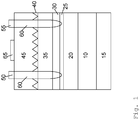
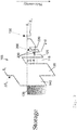
- the exemplary embodiment of Figure 1 consists of a quantumwell modulation doped field-effect transistor with a single InAs/GaAs QD layer in close vicinity to the 2DHG.
- a schematic cross section of the layer structure is shown in Figure 1 .
- a 1 ⁇ m thick undoped GaAs buffer layer 10 was grown first on an undoped GaAs substrate 15.
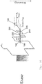
- Figure 2 schematically shows the valence band of the structure for the three memory operations: storage, writing, and erasing.
- the binding potential of holes in the QDs represents the emission barrier, needed to store a logical "1".
- a capture barrier is necessary, which is formed by the band-bending of the Schottky contact.
- the charged QDs act as Coulomb scattering centers, reducing the mobility of the 2DHG.
- Gauss' law it was predicted that the transfer of holes in QDs lead to a reduction in the carrier density in the 2DHG.
- Both the lowered charge carrier density and the decreased mobility reduce the conductance during the down sweep, resulting in a lower current trace compared to the up sweep.
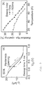
- the maximum hysteresis opening with respect to the up sweep is shown in Fig. 3(b) as a function of temperature for two different sweep times. Using a sweep time of 1 ms, the hysteresis opening drops from 32% at 20 K to almost zero at 85 K. The descent has its origin in the reduced charge carrier storage time of QDs with increasing temperature, i.e., at higher temperatures more holes are emitted during the down sweep.
- Figure 4 shows the transients at 50 K for three different storage voltages (0, 0.4, and 0.7 V).
- the upper transients represent hole capture into initially empty QDs, leading to a decrease in the conductance of the 2DHG and, hence, to a decrease in the drain current.
- the lower transients represent hole emission out of fully occupied QDs and, thus, the drain current increases to the equilibrium state.
- a change of the storage voltage from 0 to 0.4 V and further to 0.7 V causes multiple effects ( Figs. 4(a)-4(c) ); the time constants of both transients increase, the amplitude of the capture transient is reduced, and the amplitude of the emission transient is increased.
- Figs. 4(a)-4(c) the valence band profiles for the three storage voltages are shown.
- the amplitudes of the transients represent the amount of transferred holes and are correlated with the number of levels which are below the Fermi level (for capture) and above the Fermi level (for emission).
- a larger positive storage voltage shifts the Fermi level toward the QD ground state and, hence, more holes are emitted, less holes are captured, and thus the amplitudes vary.
- This saturation has presently its origin in a parasitic cut-off frequency of about 2 MHz of the RC low pass of our present devices. Much faster write times are expected for smaller devices having larger parasitic cut-off frequencies.
- the erase times are shown in Fig. 5(b) .
- a minimum erase time of 350 ns at 50 K was obtained for an erase pulse of 2.5 V.
- the temperature dependence of the write and erase times reflects again the increased thermal capture and emission rates at higher temperatures.
- Figure 6 shows a memory 105 comprising a strained double-heterostructure 110 having an inner semiconductor layer 115 which may consist of Ga(As,Sb) and which is sandwiched between two outer semiconductor layers 120 and 125.
- the outer semiconductor layers 120 and 125 may consist of (Al,Ga)As.
- the at least one quantum dot Due to the lattice strain, the at least one quantum dot has an emission barrier Eb of 1,15 eV or higher, and provides an energy state density of at least three energy states per 1000 nm 3 . All of the at least three energy states are located in an energy band ⁇ Wb of 50 meV or less. The energy band ⁇ Wb is provided such that each of said at least three energy states is capable of storing two holes.
- the memory of Figure 6 further comprises an intermediate layer 140 which is arranged between the gate electrode 135 of the field effect transistor and the strained double-heterostructure 110.
- the intermediate layer 140 has a smaller band gap than the adjacent outer semiconductor layer 120 of the strained double-heterostructure 110.
- the smaller band gap provides a conduction band discontinuity ⁇ E L at the interface between the intermediate layer 140 and the adjacent outer semiconductor layer 120.
- the conduction band discontinuity ⁇ E L prevents electrons originating from gate 135 to get into the outer semiconductor layer 120 if a positive bias voltage is applied.
- the conduction band discontinuity ⁇ E L avoids recombination of electrons and holes in the inner semiconductor layer 115.
- the gate contact of the field effect transistor is preferably an ohmic contact, and the intermediate layer 140 is preferably n-doped.
- Figure 8 shows the memory 105 after applying an erase-voltage to the strained double-heterostructure. It can be seen that the holes 185 stored in the energy states of the quantum dot may tunnel through the energy barrier 190 and reach the 2-dimensional hole gas layer 130.
- the third embodiment comprises a semiconductor superlattice 200 which is arranged between the 2-dimensional hole gas layer 130 and the outer semiconductor layer 125.
- the semiconductor superlattice 200 comprises two quantum wells 210 and 220. Each quantum well 210 and 220 provides at least one energy state 230.
- the erase process is based on hole tunneling through the entire emission barrier.
- the erase time depends on the height of the emission barrier.
- an emission barrier of 1.15 eV or higher high electric fields in the range of MV/cm are needed to reach fast erase times [11]. This high electric fields lead to a high power consumption of the memory cell and to a low endurance, as defects in the lattice could be generated.
Landscapes
- Engineering & Computer Science (AREA)
- Microelectronics & Electronic Packaging (AREA)
- Power Engineering (AREA)
- Physics & Mathematics (AREA)
- Ceramic Engineering (AREA)
- Condensed Matter Physics & Semiconductors (AREA)
- General Physics & Mathematics (AREA)
- Computer Hardware Design (AREA)
- Nanotechnology (AREA)
- Chemical & Material Sciences (AREA)
- Theoretical Computer Science (AREA)
- Crystallography & Structural Chemistry (AREA)
- Mathematical Physics (AREA)
- Semiconductor Memories (AREA)
- Non-Volatile Memory (AREA)
- Junction Field-Effect Transistors (AREA)
Description
- The present invention relates to memories, and more particularly to semiconductor memories.
- Distinct types of memories will combine the advantages of nonvolatility of the Flash-memory [1] and the performance and endurance of the dynamic random access memory (DRAM) [2]. A large variety of such memory concepts has been proposed using different approaches, like FeRAM, MRAM, PCRAM, etc. [3]. One of the most promising options for chargebased memories is based on self-organized quantum dots (QDs) as memory units. Memory operation for III-V QD structures has been demonstrated, either based on optically [4-6] or electrically controlled charge storage [7-9]. A quantum dot-based memory device is disclosed in [12]. A tunneling emission from self-organized In (Ga)As/GaAs quantum dots observed via time-resolved capacitance measurements is described in [13]. Another memory based on semiconductor material is described in [14] .
- An objective of the present invention is to provide a memory which provides a long storage time in combination with fast write and erase time and high endurance.
- An embodiment of the invention relates to a memory according to
claim 1. - Preferably, each of said at least three energy states is capable of storing two charge carriers.
- Each of said at least three energy states preferably stores holes and is capable of storing two holes. Energy states of confined holes are more closely spaced than those of electrons, and thus show a much higher carrier density in terms of their energy distribution than electrons. As such, energy states for holes can store more carriers per unit volume than energy states for electrons. A larger number of stored carriers per binary information unit increase the reliability of the stored information.
- According to a preferred embodiment, said at least three energy states are energetically located above the Fermi-level if the strained double-heterostructure is unbiased.
- The hole-energy states of the two quantum wells may be located above the Fermi-level if the strained double-heterostructure is unbiased.
- An intermediate layer may be arranged between the gate electrode of the field effect transistor and the strained double-heterostructure, said intermediate layer having a smaller band gap than the adjacent outer semiconductor layer of the strained double-heterostructure.
- A conduction band discontinuity may be positioned at the interface between the intermediate layer and the adjacent outer semiconductor layer. Such a conduction band discontinuity may prevent electrons from reaching the strained double-heterostructure when the strained double-heterostructure is biased.
- The gate electrode of the field effect transistor may be an ohmic contact, and the intermediate layer may be n-doped.
- Alternatively, the gate electrode of the field effect transistor may be a Schottky contact.
- The quantum dots in the inner semiconductor layer may be arranged in an array.
- In order that the manner in which the above-recited and other advantages of the invention are obtained will be readily understood, a more particular description of the invention briefly described above will be rendered by reference to specific embodiments thereof which are illustrated in the appended figures. Understanding that these figures depict only typical embodiments of the invention and are therefore not to be considered to be limiting of its scope, the invention will be described and explained with additional specificity and detail by the use of the accompanying drawings in which
- Figure 1
- shows a first embodiment of a memory ,
- Figure 2
- shows a schematic illustration of the storage (a), write (b), and erase (c) operations in the embodiment of
Figure 1 , - Figure 3
- shows (a) hysteresis at 50 K, and (b) temperature dependence of the hysteresis opening for a sweep time of 1 and 100 ms, respectively,
- Figure 4
- shows drain current transients at 50 K at a storage voltage of 0 V (a), 0.4 V (b), and 0.7 V (c), wherein insets show the valence band profiles at the given voltages,
- Figure 5
- shows write times (a) and erase times (b) in dependence on the pulse voltage,
- Figure 6
- shows a second embodiment of a memory in an unbiased state,
- Figure 7
- shows the second embodiment during write operation,
- Figure 8
- shows the second embodiment during erase operation,
- Figure 9
- shows a third embodiment of a memory in an unbiased state, the third embodiment being an exemplary embodiment according to the present invention,
- Figure 10
- shows the third embodiment during erase operation, and
- Figure 11
- shows achievable storage times for various material systems.
- Only the third embodiment is an exemplary embodiment according to the invention; the first and second embodiments are not exemplary embodiments according to the invention, but useful for its understanding.
- The preferred embodiments of the present invention will be best understood by reference to the drawings, wherein identical or comparable parts are designated by the same reference signs throughout.
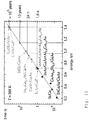
- The embodiments described below are based on III-V quantum dots (QD) which allow the storage of holes. Hole storage offers significant advantages with respect to scalability and storage time. The energy levels of confined holes in a QD are much more closely spaced than those of electrons due to their larger effective mass. Thus, at least one order of magnitude more holes can be stored in a given volume than electrons. In addition, hole-confining type-II systems (e.g., GaSb/AlGaAs QDs) provide huge hole localization energies leading to storage times of more than ten years at room temperature, a basic prerequisite for a nonvolatile memory.
- The localization energies and therefore the emission barriers for confined holes in the ground state of the QD are summarized in
Fig. 11 for different III-V QDs [10]. The storage time shows an exponential dependence on the localization energy as predicted by the common rate equation of thermally activated emission. The storage time increases by one order of magnitude for an increase of the localization energy of about 50 meV. It can be seen that memories based on Ga(As,Sb)/(Al,Ga)As and Ga(As,Sb)/GaP may reach storage times above 10 years. - A first exemplary embodiment relates to an InAs/GaAs QD memory which uses holes as charge carriers instead of electrons. For monitoring, the commonly used electron channel is replaced by a 2D hole gas (2DHG) embedded underneath the QD layer. Static and time-resolved measurements of storage, write, and erase times demonstrate the feasibility of the hole-based QD-memory concept.
- The exemplary embodiment of
Figure 1 consists of a quantumwell modulation doped field-effect transistor with a single InAs/GaAs QD layer in close vicinity to the 2DHG. A schematic cross section of the layer structure is shown inFigure 1 . A 1 µm thick undopedGaAs buffer layer 10 was grown first on anundoped GaAs substrate 15. The 2DHG was formed with 40 nm p-doped (p=2*1018 cm-3)GaAs layer 20, a 7 nm thick undopedGaAs spacer layer 25, and a 8 nm thick In0.25Ga0.75Asquantum well 30. Subsequently, a 20 nmundoped GaAs layer 35 was deposited, followed by a single InAs QD layer 40 (nominally ∼1.8 ML). Finally, the structure was completed by a 180 nmundoped GaAs cap 45. - The heterostructure was processed into Hall bars with an active area of 310*460 µm2 using chemical wet etching (see
Figure 1 (b) ). - The source and drain
areas ohmic contacts 60 down to the 2DHG. Thegate 65 was formed by Ni/Au as a Schottky contact. Hall measurements at gate electrode 70 yielded a charge carrier density and a mobility of the 2DHG at 77 K of 8*1011 cm-2 and 4350 cm2/Vs, respectively. -
Figure 2 schematically shows the valence band of the structure for the three memory operations: storage, writing, and erasing. At the storage position (Fig. 2(a) ), the binding potential of holes in the QDs represents the emission barrier, needed to store a logical "1". To store a logical "0" (defined as empty QDs) a capture barrier is necessary, which is formed by the band-bending of the Schottky contact. - The storage time for both logic states is limited by the emission and capture processes of the QDs. In the structure, thermally assisted tunneling across the emission and capture barriers initiates the discharging and charging processes. The emission and capture rates depend on the barrier height (i.e., localization energy and capture barrier height), the temperature, and the electric field. To write a logical "1" (
Fig. 2(b) ), a negative bias is applied to the gate. This completely eliminates the capture barrier formed by the band-bending and fast write times down to nanoseconds can be realized. Thus, the QD-memory concept solves the drawbacks of Flash's SiO2 barriers by using a large barrier height which can, however, be decreased to almost zero during write operation. Write times similar to those of DRAMs or even shorter are possible. - To erase the information (
Fig. 2(c) ) the electric field at the position of the QDs is increased by applying a positive bias such that tunnel emission occurs. The read-out of the stored information is done via the 2DHG below the QD layer. Carriers stored in the QDs reduce the charge density and the mobility in the 2DHG resulting in a lower conductance of the 2DHG when the QDs are occupied. To investigate the influence of holes stored in the QDs on the conductance of the 2DHG, the drain current ID versus gate voltage V G was measured in the dark with a fixed drain-source voltage of 100 mV. -
Figure 3(a) shows the measured hysteresis at a temperature of 50 K. The measurement cycle starts with a 10 ms long charging pulse (V G=-1 V), which shifts the QD states below the Fermi level, charging them with holes from the 2DHG (seeFig. 2(b) ). - When the gate voltage is now swept to 1.5 V the drain current decreases until the 2DHG is pinched off at about 1.1 V. During the down sweep the QDs remain occupied if the sweep time is shorter than the hole storage time in the QDs.
- At V G =1.5 V the QD states are far above the Fermi level (see
Fig. 2(c) ) and tunnel emission discharges the QDs. When the gate voltage is swept back to -1 V a larger current is observed leading to a distinct hysteresis opening. The hysteresis originates from the influence of holes stored in the QDs on the conductance of the 2DHG during the down sweep. - The charged QDs act as Coulomb scattering centers, reducing the mobility of the 2DHG. In addition, using Gauss' law it was predicted that the transfer of holes in QDs lead to a reduction in the carrier density in the 2DHG. Both the lowered charge carrier density and the decreased mobility reduce the conductance during the down sweep, resulting in a lower current trace compared to the up sweep. The maximum hysteresis opening with respect to the up sweep is shown in
Fig. 3(b) as a function of temperature for two different sweep times. Using a sweep time of 1 ms, the hysteresis opening drops from 32% at 20 K to almost zero at 85 K. The descent has its origin in the reduced charge carrier storage time of QDs with increasing temperature, i.e., at higher temperatures more holes are emitted during the down sweep. - In [7] a high temperature memory effect due to deep levels is reported for a different InAs QD-structure. Here, the absence of such high temperature memory effects proves that not deep levels but in fact the QDs act as memory units. This conclusion is confirmed by previous investigations of hole emission from similar InAs/GaAs QDs by deep level transient spectroscopy, which resulted in a thermal emission time constant of 5 ms at 90 K for the QD hole ground state, in agreement with the disappearance of the hysteresis at 85 K for a sweep time of 1 ms. A sweep time of 100 ms further reduces the hysteresis opening as compared to 1 ms, since more holes, stored in the QDs, are emitted during the slower down sweep.
- An increased maximum hysteresis opening is expected using larger QD densities and/or multiple QD layers. The memory operation of the QD-memory prototype is studied by time-resolved measurements of the drain current at different storage voltages V St, with either initially occupied or empty QDs. The QDs are charged or discharged by applying a gate voltage of -0.8 or 2 V, respectively.
- After this initialization of the logical "1" or "0", the gate voltage was abruptly changed to the storage voltage and the drain current was measured as a function of time.
-
Figure 4 shows the transients at 50 K for three different storage voltages (0, 0.4, and 0.7 V). The upper transients represent hole capture into initially empty QDs, leading to a decrease in the conductance of the 2DHG and, hence, to a decrease in the drain current. The lower transients represent hole emission out of fully occupied QDs and, thus, the drain current increases to the equilibrium state. A change of the storage voltage from 0 to 0.4 V and further to 0.7 V causes multiple effects (Figs. 4(a)-4(c) ); the time constants of both transients increase, the amplitude of the capture transient is reduced, and the amplitude of the emission transient is increased. These effects can be explained by the changes of the capture and emission processes when applying a positive storage voltage to the structure. - On the right hand side of
Figs. 4(a)-4(c) the valence band profiles for the three storage voltages are shown. The amplitudes of the transients represent the amount of transferred holes and are correlated with the number of levels which are below the Fermi level (for capture) and above the Fermi level (for emission). A larger positive storage voltage shifts the Fermi level toward the QD ground state and, hence, more holes are emitted, less holes are captured, and thus the amplitudes vary. - The prolongation of the time constants is also related to the Fermi level shift as it leads to an increased capture and emission barrier height (Ebar in
Fig. 4 ). - The write and erase times of the memory structure were measured. To determine write and erase times, a method was used which allowed to study emission from or capture into QDs across an enlarged span of time constants. The hysteresis opening at a storage position of 0.4 V was measured after applying write/erase pulses with successively reduced pulse widths down to 10 ns. When the pulse width was too short for any charging/discharging of the QDs, the hysteresis opening vanished. The write/erase times were defined as the pulse width, at which the hysteresis opening drops to 50% of the maximum value.
-
Figure 5(a) shows the write time in dependence on the write pulse voltage at 20 and 50 K. A more negative write pulse leads to a reduction in the capture barrier during writing and, hence, the write time decreases exponentially. For write pulses larger than |0.5| V the write time starts to saturate and reaches a minimum at 80 ns for a write pulse of -1.75 V. - This saturation has presently its origin in a parasitic cut-off frequency of about 2 MHz of the RC low pass of our present devices. Much faster write times are expected for smaller devices having larger parasitic cut-off frequencies.
- The erase times are shown in
Fig. 5(b) . A minimum erase time of 350 ns at 50 K was obtained for an erase pulse of 2.5 V. The temperature dependence of the write and erase times reflects again the increased thermal capture and emission rates at higher temperatures. - Summarizing, the first exemplary embodiment relates to a hole based memory device using InAs/GaAs QDs for charge carrier storage. Charging and discharging of the QDs are clearly controlled by a gate voltage. The read-out of the stored information uses a 2DHG, with a relative hysteresis opening up to 32%. Write times down to 80 ns - only a factor of 8 larger than for a typical DRAM - and erase times of 350 ns - four orders of magnitude faster than for a typical Flash memories - were demonstrated. The results support the assumption that the QDs act as memory.
- A second exemplary embodiment will be explained in further detail with reference to
Figures 6 - 8 . -
Figure 6 shows amemory 105 comprising a strained double-heterostructure 110 having aninner semiconductor layer 115 which may consist of Ga(As,Sb) and which is sandwiched between two outer semiconductor layers 120 and 125. The outer semiconductor layers 120 and 125 may consist of (Al,Ga)As. - The lattice constant of the
inner semiconductor layer 115 differs from the lattice constants of the outer semiconductor layers 120 and 125, such that lattice strain is generated. The resulting lattice strain in the double-heterostructure 110 induces the formation of at least one quantum dot inside the inner semiconductor layer, said at least one quantum dot providing at least threeenergy states 186 capable of storing charge carriers therein. - Due to the lattice strain, the at least one quantum dot has an emission barrier Eb of 1,15 eV or higher, and provides an energy state density of at least three energy states per 1000 nm3. All of the at least three energy states are located in an energy band ΔWb of 50 meV or less. The energy band ΔWb is provided such that each of said at least three energy states is capable of storing two holes.
-
Figure 6 shows thememory 105 in an unbiased state. It can be seen that the at least three energy levels of holes are energetically above than the Fermi-level Ef. - Moreover,
Figure 6 shows a 2-dimensionalhole gas layer 130 which is capable of transporting holes for charging or discharging the at least one quantum dot. The 2-dimensionalhole gas layer 130 is part of a field effect transistor of the memory. Thegate electrode 135 of the field effect transistor allows applying a voltage to the strained double-heterostructure 110. - The memory of
Figure 6 further comprises anintermediate layer 140 which is arranged between thegate electrode 135 of the field effect transistor and the strained double-heterostructure 110. Theintermediate layer 140 has a smaller band gap than the adjacentouter semiconductor layer 120 of the strained double-heterostructure 110. The smaller band gap provides a conduction band discontinuity ΔEL at the interface between theintermediate layer 140 and the adjacentouter semiconductor layer 120. The conduction band discontinuity ΔEL prevents electrons originating fromgate 135 to get into theouter semiconductor layer 120 if a positive bias voltage is applied. Thus, the conduction band discontinuity ΔEL avoids recombination of electrons and holes in theinner semiconductor layer 115. - The gate contact of the field effect transistor is preferably an ohmic contact, and the
intermediate layer 140 is preferably n-doped. -
Figure 7 shows thememory 105 ofFigure 6 after applying a write-voltage to the strained double-heterostructure. It can be seen that holes 185 may leave the 2-dimensionalhole gas layer 130 and drop into the energy states 186 of the quantum dot located in theinner semiconductor layer 115. -
Figure 8 shows thememory 105 after applying an erase-voltage to the strained double-heterostructure. It can be seen that theholes 185 stored in the energy states of the quantum dot may tunnel through theenergy barrier 190 and reach the 2-dimensionalhole gas layer 130. - A third exemplary embodiment will be explained in further detail with reference to
Figures 9-10 . -
Figure 9 shows amemory 105 which comprises a strained double-heterostructure 110 having aninner semiconductor layer 115 which is sandwiched between two outer semiconductor layers 120 and 125. Anintermediate layer 140 is arranged between agate electrode 135 and theouter semiconductor layer 120. Furthermore, thememory 105 comprises a 2-dimensionalhole gas layer 130 which is capable of transporting holes for charging or discharging at least one quantum dot positioned in theinner semiconductor layer 115. Insofar, the third exemplary embodiment corresponds to the second exemplary embodiment described with respect toFigures 6-8 . - In addition to the second embodiment, the third embodiment comprises a
semiconductor superlattice 200 which is arranged between the 2-dimensionalhole gas layer 130 and theouter semiconductor layer 125. Thesemiconductor superlattice 200 comprises twoquantum wells energy state 230. - In
Figure 9 , the strained double-heterostructure 110 is unbiased. It can be seen that the energetic positions of the energy states 230 of thequantum wells semiconductor superlattice 200 and thus not reach the 2-dimensionalhole gas layer 130. -
Figure 10 shows the third embodiment after applying an external erase bias voltage to the strained double-heterostructure. Due to the bias voltage, the energy states 230 of thequantum wells holes 185 to tunnel from the quantum dot through thesemiconductor superlattice 200 based on resonant tunneling. The holes can reach the 2-dimensionalhole gas layer 130 and the energy states of the at least one quantum dot are emptied. - In the first and second embodiment, the erase process is based on hole tunneling through the entire emission barrier. Hence, the erase time depends on the height of the emission barrier. Regarding an emission barrier of 1.15 eV or higher, high electric fields in the range of MV/cm are needed to reach fast erase times [11]. This high electric fields lead to a high power consumption of the memory cell and to a low endurance, as defects in the lattice could be generated.
- The third embodiment solves these problems. There, the erase process is done by resonant tunneling through the superlattice. Only a small voltage is needed to align the energy states of the quantum well to allow resonant hole tunneling. As a consequence the electric field is increased just marginally. Therewith, both problems - the high power consumtion and the low endurance - are solved. A memory with long storage time in combination with a fast erase time and high endurance is feasible.
-
Figure 11 shows achievable storage times for various material systems. It can be seen that memories based on Ga(As,Sb)/(Al,Ga)As and Ga(As,Sb)/GaP may reach storage times above 10 years. -
- [1] P. Pavan, R. Bez, P. Olivo, and E. Zanoni, Proc. IEEE 85, 1248 (1997).
- [2] R. Waser, Nanoelectronics and Information Technology _Wiley, Weinheim, 2003.
- [3] G. W. Burr, B. N. Kurdi, J. C. Scott, C. H. Lam, K. Go-palakrishnan, and R. S. Shenoy, IBM J. Res. Dev. 52, 449 (2008).
- [4] J. J. Finley, M. Skalitz, M. Arzberger, A. Zrenner, G. Böhm, and G. Abstreiter, Appl. Phys. Lett. 73, 2618 _1998_.
- [5] K. Koike, K. Saitoh, S. Li, S. Sasa, M. Inoue, and M. Yano, Appl. Phys. Lett. 76, 1464 (2000).
- [6] H. Pettersson, L. Baath, N. Carlson, W. Seifert, and L. Samuelson, Appl. Phys. Lett. 79, 78 (2001).
- [7] C. Balocco, A. M. Song, and M. Missous, Appl. Phys. Lett. 85, 5911 (2004).
- [8] D. Nataraj, N. Ooike, J. Motohisa, and T. Fukui, Appl. Phys. Lett. 87,193103 (2005).
- [9] C. R. Muller, L. Worschech, J. Heinrich, S. Höfling, and A. Forchel, Appl. Phys. Lett. 93, 063502 (2008).
- [10] A. Marent, M. Geller, A. Schliwa, D. Feise, K. Pötschke, and D. Bimberg, N. Akçay and N. Oncan, Appl. Phys. Lett. 91, 242109 (2007).
- [11] T. Nowozin, A. Marent, M. Geller, N. Akçay, N. Oncan, D. Bimberg, Appl. Phys. Lett. 94, 4, 042108 (2009)
- [12] A Marent, T Nowozin, M Geller, D Bimberg "The QD-Flash: a quantum dot-based memory device", 2011 IOP Publishing Ltd, vol. 26, no. 1, doi:10.1088/0268-1242/26/1/014026, ISSN 0268-1242, page 14026
- [13] M. Geller, E. Stock, C. Kapteyn, R. L. Sellin, and D. Bimberg, "Tunneling emission from self-organized In(Ga)As/GaAs quantum dots observed via time-resolved capacitance measurements", Physical Review, American Institute of Physics, US, 20060515, vol. 73, no. 20, doi: 10. 1103/ PHYSREVB.73.205331, ISSN 0163-1829, page 205331,
- [14]
DE 10 2006 059 110 A1 -
- 10
- buffer layer
- 15
- substrate
- 20
- layer
- 25
- spacer layer
- 30
- quantum well
- 35
- layer
- 40
- QD layer
- 45
- cap
- 50
- source
- 55
- drain
- 60
- ohmic contact
- 65
- gate
- 105
- memory
- 110
- strained double-heterostructure
- 115
- inner semiconductor layer
- 120
- outer semiconductor layer
- 125
- outer semiconductor layer
- 130
- 2-dimensional hole gas layer
- 135
- gate electrode
- 140
- intermediate layer
- 185
- hole
- 186
- energy state
- 190
- energy barrier
- 200
- semiconductor superlattice
- 210
- quantum well
- 220
- quantum well
- 230
- energy state
- ΔEL
- conduction band discontinuity
- EF
- Fermi energy
- EV
- valence band
- EL
- conduction band
- ΔWb
- energy band
Claims (4)
- Memory (105) comprising a field effect transistor, said field effect transistor comprising a strained double-heterostructure (110) having an inner semiconductor layer (115) which is sandwiched between two outer semiconductor layers (120, 125), wherein the inner semiconductor (115) layer consists of Ga(As, Sb) and the two outer semiconductor layers (120, 125) consist of (Al, Ga)As, and a gate electrode (135) adapted to apply a voltage to the strained double-heterostructure (110), said gate electrode (135) facing one of said outer semiconductor layers (120),- wherein the lattice constant of the inner semiconductor layer (115) differs from the lattice constants of the outer semiconductor layers (120, 125), the resulting lattice strain in the double-heterostructure inducing the formation of at least one quantum dot inside the inner semiconductor layer (115), said at least one quantum dot being capable of storing charge carriers therein, and- wherein, due to the lattice strain, the at least one quantum dot has an emission barrier of 1,15 eV or higher and,- wherein the memory (105) comprises a 2-dimensional hole gas layer (130) capable of transporting holes (185) for charging or discharging the at least one quantum dot,characterized in that- the at least one quantum dot provides an energy state density of at least three energy states per 1000 nm3, all said at least three energy states being located in an energy band of 50 meV or less,- wherein a semiconductor superlattice (200) is arranged between said 2-dimensional hole gas layer (130) and the other one of said outer semiconductor layers (125),- wherein said semiconductor superlattice (200) comprises at least two quantum wells (210, 220), each of which providing at least one energy state (230),- wherein the energetic positions of the energy states (230) of the at least two quantum wells (210, 220) differ from another if the strained double-heterostructure (110) is unbiased,- wherein the energy states (230) of the at least two quantum wells (210, 220) are shiftable relative to each other and relative to the energy states (186) of the at least one quantum dot in response to an external bias voltage to the strained double-heterostructure (110) via said gate electrode (135),- wherein, in response to an erase voltage applied to the strained double-heterostructure (110) via said gate electrode (135), the energy states (230) of the at least two quantum wells (210, 220) are alignable such that holes (185) can tunnel from the at least one quantum dot through the semiconductor superlattice (200) based on resonant tunneling, and- wherein, in an unbiased state, the energy levels of the at least two quantum wells (210, 220) mismatch and resonance tunneling of holes (185) is disabled.
- Memory (105) of claim 1 wherein an intermediate layer (140) is arranged between the gate electrode (135) of the field effect transistor and said one of said outer semiconductor layers (120), said intermediate layer (140) having a band gap smaller than said one of said outer semiconductor layers (120) of the strained double-heterostructure (110).
- Memory (105) of claim 2,- wherein the gate electrode of the field effect transistor is an ohmic contact; and- wherein the intermediate layer (140) is n-doped.
- Memory (105) of claim 2 wherein the gate electrode of the field effect transistor is a Schottky contact.
Applications Claiming Priority (2)
| Application Number | Priority Date | Filing Date | Title |
|---|---|---|---|
| US12/970,744 US8331142B2 (en) | 2010-12-16 | 2010-12-16 | Memory |
| PCT/EP2011/072181 WO2012080076A1 (en) | 2010-12-16 | 2011-12-08 | Memory device comprising a strained semiconductor double-heterostructure and quantum dots |
Publications (2)
| Publication Number | Publication Date |
|---|---|
| EP2652789A1 EP2652789A1 (en) | 2013-10-23 |
| EP2652789B1 true EP2652789B1 (en) | 2020-07-08 |
Family
ID=45476459
Family Applications (1)
| Application Number | Title | Priority Date | Filing Date |
|---|---|---|---|
| EP11807878.1A Active EP2652789B1 (en) | 2010-12-16 | 2011-12-08 | Memory device comprising a strained semiconductor double-heterostructure and quantum dots |
Country Status (5)
| Country | Link |
|---|---|
| US (1) | US8331142B2 (en) |
| EP (1) | EP2652789B1 (en) |
| JP (1) | JP5689540B2 (en) |
| KR (1) | KR101567994B1 (en) |
| WO (1) | WO2012080076A1 (en) |
Families Citing this family (4)
| Publication number | Priority date | Publication date | Assignee | Title |
|---|---|---|---|---|
| US9082637B2 (en) * | 2012-08-17 | 2015-07-14 | The University Of Connecticut | Optoelectronic integrated circuit |
| JP6415956B2 (en) | 2014-12-09 | 2018-10-31 | 東芝メモリ株式会社 | Semiconductor memory device and control method thereof |
| GB201907540D0 (en) | 2019-05-29 | 2019-07-10 | Univ Of Lancaster | Improvements relating to electronic memory devices |
| CN116867276B (en) * | 2023-06-07 | 2023-12-12 | 合肥美镓传感科技有限公司 | Gallium nitride non-volatile memory device and preparation method thereof |
Family Cites Families (7)
| Publication number | Priority date | Publication date | Assignee | Title |
|---|---|---|---|---|
| JP3672678B2 (en) * | 1996-04-05 | 2005-07-20 | 富士通株式会社 | Quantum semiconductor device and manufacturing method thereof |
| US6281519B1 (en) * | 1997-08-13 | 2001-08-28 | Fujitsu Limited | Quantum semiconductor memory device including quantum dots |
| JP4116722B2 (en) | 1998-12-28 | 2008-07-09 | 富士通株式会社 | Quantum semiconductor memory device and method for reading quantum semiconductor memory device |
| KR100377498B1 (en) * | 2000-09-09 | 2003-03-26 | 한국과학기술연구원 | Method for fabricating semiconductor device of quantum dots structure and an semiconductor device fabricated thereby |
| EP2192616B1 (en) * | 2002-05-22 | 2012-12-05 | Fujitsu Limited | Quantum semiconductor device and method for fabricating the same |
| US7750425B2 (en) * | 2005-12-16 | 2010-07-06 | The Trustees Of Princeton University | Intermediate-band photosensitive device with quantum dots embedded in energy fence barrier |
| DE102006059110A1 (en) | 2006-12-08 | 2008-06-12 | Technische Universität Berlin | Memory cell and method for storing data |
-
2010
- 2010-12-16 US US12/970,744 patent/US8331142B2/en active Active
-
2011
- 2011-12-08 EP EP11807878.1A patent/EP2652789B1/en active Active
- 2011-12-08 WO PCT/EP2011/072181 patent/WO2012080076A1/en active Application Filing
- 2011-12-08 JP JP2013543654A patent/JP5689540B2/en active Active
- 2011-12-08 KR KR1020137011088A patent/KR101567994B1/en active IP Right Grant
Non-Patent Citations (1)
| Title |
|---|
| None * |
Also Published As
| Publication number | Publication date |
|---|---|
| US8331142B2 (en) | 2012-12-11 |
| JP2014506002A (en) | 2014-03-06 |
| KR101567994B1 (en) | 2015-11-10 |
| KR20140027904A (en) | 2014-03-07 |
| EP2652789A1 (en) | 2013-10-23 |
| WO2012080076A1 (en) | 2012-06-21 |
| JP5689540B2 (en) | 2015-03-25 |
| US20120155165A1 (en) | 2012-06-21 |
Similar Documents
| Publication | Publication Date | Title |
|---|---|---|
| Marent et al. | The QD-Flash: a quantum dot-based memory device | |
| US7342277B2 (en) | Transistor for non volatile memory devices having a carbon nanotube channel and electrically floating quantum dots in its gate dielectric | |
| EP2652789B1 (en) | Memory device comprising a strained semiconductor double-heterostructure and quantum dots | |
| Nowozin et al. | Materials for future quantum dot-based memories | |
| KR20120124697A (en) | Non-volatile memory device using graphene gate electrode | |
| Marent et al. | Hole-based memory operation in an InAs/GaAs quantum dot heterostructure | |
| JPH08148669A (en) | Semiconductor device | |
| EP0674798B1 (en) | Memory device | |
| US7948822B2 (en) | Memory cell, and method for storing data | |
| US20140231820A1 (en) | Memory device using graphene as charge-trap layer and method of operating the same | |
| US10243086B2 (en) | Electronic memory devices | |
| Bimberg et al. | Antimony-based quantum dot memories | |
| US11270999B2 (en) | Capacitorless DRAM cell | |
| CN114080682A (en) | Improvements relating to electronic memory devices | |
| Chang et al. | FinFlash with buried storage ONO layer for flash memory application | |
| US9424925B2 (en) | Memory cell | |
| Bonato | Towards non-volatility in quantum-dot-based memories | |
| Geller et al. | Quantum Dots for Memories | |
| Lingalugari et al. | Quantum Dot Floating Gate Nonvolatile Random Access Memory Using Ge Quantum Dot Channel for Faster Erasing | |
| Nowozin et al. | Quantum Dot-Based Flash Memories | |
| JP4007560B2 (en) | Semiconductor device | |
| Oh et al. | Room-temperature memory operation of AlGaAs/GaAs high electron mobility transistors with InAs quantum dots embedded in the channel | |
| Kasper et al. | Tunneling Phenomena | |
| JPS62226658A (en) | Semiconductor device |
Legal Events
| Date | Code | Title | Description |
|---|---|---|---|
| PUAI | Public reference made under article 153(3) epc to a published international application that has entered the european phase |
Free format text: ORIGINAL CODE: 0009012 |
|
| 17P | Request for examination filed |
Effective date: 20130703 |
|
| AK | Designated contracting states |
Kind code of ref document: A1 Designated state(s): AL AT BE BG CH CY CZ DE DK EE ES FI FR GB GR HR HU IE IS IT LI LT LU LV MC MK MT NL NO PL PT RO RS SE SI SK SM TR |
|
| DAX | Request for extension of the european patent (deleted) | ||
| 17Q | First examination report despatched |
Effective date: 20150202 |
|
| STAA | Information on the status of an ep patent application or granted ep patent |
Free format text: STATUS: EXAMINATION IS IN PROGRESS |
|
| RIC1 | Information provided on ipc code assigned before grant |
Ipc: H01L 29/06 20060101ALI20190726BHEP Ipc: H01L 29/66 20060101ALI20190726BHEP Ipc: H01L 29/12 20060101AFI20190726BHEP Ipc: G11C 16/04 20060101ALI20190726BHEP Ipc: H01L 29/788 20060101ALI20190726BHEP Ipc: B82Y 10/00 20110101ALI20190726BHEP Ipc: H01L 21/336 20060101ALI20190726BHEP Ipc: H01L 29/80 20060101ALI20190726BHEP Ipc: H01L 29/68 20060101ALI20190726BHEP |
|
| GRAP | Despatch of communication of intention to grant a patent |
Free format text: ORIGINAL CODE: EPIDOSNIGR1 |
|
| STAA | Information on the status of an ep patent application or granted ep patent |
Free format text: STATUS: GRANT OF PATENT IS INTENDED |
|
| INTG | Intention to grant announced |
Effective date: 20190911 |
|
| GRAJ | Information related to disapproval of communication of intention to grant by the applicant or resumption of examination proceedings by the epo deleted |
Free format text: ORIGINAL CODE: EPIDOSDIGR1 |
|
| STAA | Information on the status of an ep patent application or granted ep patent |
Free format text: STATUS: EXAMINATION IS IN PROGRESS |
|
| INTC | Intention to grant announced (deleted) | ||
| GRAP | Despatch of communication of intention to grant a patent |
Free format text: ORIGINAL CODE: EPIDOSNIGR1 |
|
| STAA | Information on the status of an ep patent application or granted ep patent |
Free format text: STATUS: GRANT OF PATENT IS INTENDED |
|
| INTG | Intention to grant announced |
Effective date: 20200205 |
|
| GRAS | Grant fee paid |
Free format text: ORIGINAL CODE: EPIDOSNIGR3 |
|
| GRAA | (expected) grant |
Free format text: ORIGINAL CODE: 0009210 |
|
| STAA | Information on the status of an ep patent application or granted ep patent |
Free format text: STATUS: THE PATENT HAS BEEN GRANTED |
|
| AK | Designated contracting states |
Kind code of ref document: B1 Designated state(s): AL AT BE BG CH CY CZ DE DK EE ES FI FR GB GR HR HU IE IS IT LI LT LU LV MC MK MT NL NO PL PT RO RS SE SI SK SM TR |
|
| REG | Reference to a national code |
Ref country code: GB Ref legal event code: FG4D |
|
| REG | Reference to a national code |
Ref country code: AT Ref legal event code: REF Ref document number: 1289391 Country of ref document: AT Kind code of ref document: T Effective date: 20200715 Ref country code: CH Ref legal event code: EP |
|
| REG | Reference to a national code |
Ref country code: DE Ref legal event code: R096 Ref document number: 602011067684 Country of ref document: DE |
|
| REG | Reference to a national code |
Ref country code: IE Ref legal event code: FG4D |
|
| REG | Reference to a national code |
Ref country code: LT Ref legal event code: MG4D |
|
| REG | Reference to a national code |
Ref country code: AT Ref legal event code: MK05 Ref document number: 1289391 Country of ref document: AT Kind code of ref document: T Effective date: 20200708 |
|
| REG | Reference to a national code |
Ref country code: NL Ref legal event code: MP Effective date: 20200708 |
|
| PG25 | Lapsed in a contracting state [announced via postgrant information from national office to epo] |
Ref country code: NO Free format text: LAPSE BECAUSE OF FAILURE TO SUBMIT A TRANSLATION OF THE DESCRIPTION OR TO PAY THE FEE WITHIN THE PRESCRIBED TIME-LIMIT Effective date: 20201008 Ref country code: GR Free format text: LAPSE BECAUSE OF FAILURE TO SUBMIT A TRANSLATION OF THE DESCRIPTION OR TO PAY THE FEE WITHIN THE PRESCRIBED TIME-LIMIT Effective date: 20201009 Ref country code: AT Free format text: LAPSE BECAUSE OF FAILURE TO SUBMIT A TRANSLATION OF THE DESCRIPTION OR TO PAY THE FEE WITHIN THE PRESCRIBED TIME-LIMIT Effective date: 20200708 Ref country code: SE Free format text: LAPSE BECAUSE OF FAILURE TO SUBMIT A TRANSLATION OF THE DESCRIPTION OR TO PAY THE FEE WITHIN THE PRESCRIBED TIME-LIMIT Effective date: 20200708 Ref country code: BG Free format text: LAPSE BECAUSE OF FAILURE TO SUBMIT A TRANSLATION OF THE DESCRIPTION OR TO PAY THE FEE WITHIN THE PRESCRIBED TIME-LIMIT Effective date: 20201008 Ref country code: ES Free format text: LAPSE BECAUSE OF FAILURE TO SUBMIT A TRANSLATION OF THE DESCRIPTION OR TO PAY THE FEE WITHIN THE PRESCRIBED TIME-LIMIT Effective date: 20200708 Ref country code: LT Free format text: LAPSE BECAUSE OF FAILURE TO SUBMIT A TRANSLATION OF THE DESCRIPTION OR TO PAY THE FEE WITHIN THE PRESCRIBED TIME-LIMIT Effective date: 20200708 Ref country code: HR Free format text: LAPSE BECAUSE OF FAILURE TO SUBMIT A TRANSLATION OF THE DESCRIPTION OR TO PAY THE FEE WITHIN THE PRESCRIBED TIME-LIMIT Effective date: 20200708 Ref country code: PT Free format text: LAPSE BECAUSE OF FAILURE TO SUBMIT A TRANSLATION OF THE DESCRIPTION OR TO PAY THE FEE WITHIN THE PRESCRIBED TIME-LIMIT Effective date: 20201109 Ref country code: FI Free format text: LAPSE BECAUSE OF FAILURE TO SUBMIT A TRANSLATION OF THE DESCRIPTION OR TO PAY THE FEE WITHIN THE PRESCRIBED TIME-LIMIT Effective date: 20200708 |
|
| PG25 | Lapsed in a contracting state [announced via postgrant information from national office to epo] |
Ref country code: IS Free format text: LAPSE BECAUSE OF FAILURE TO SUBMIT A TRANSLATION OF THE DESCRIPTION OR TO PAY THE FEE WITHIN THE PRESCRIBED TIME-LIMIT Effective date: 20201108 Ref country code: PL Free format text: LAPSE BECAUSE OF FAILURE TO SUBMIT A TRANSLATION OF THE DESCRIPTION OR TO PAY THE FEE WITHIN THE PRESCRIBED TIME-LIMIT Effective date: 20200708 Ref country code: LV Free format text: LAPSE BECAUSE OF FAILURE TO SUBMIT A TRANSLATION OF THE DESCRIPTION OR TO PAY THE FEE WITHIN THE PRESCRIBED TIME-LIMIT Effective date: 20200708 Ref country code: RS Free format text: LAPSE BECAUSE OF FAILURE TO SUBMIT A TRANSLATION OF THE DESCRIPTION OR TO PAY THE FEE WITHIN THE PRESCRIBED TIME-LIMIT Effective date: 20200708 |
|
| PG25 | Lapsed in a contracting state [announced via postgrant information from national office to epo] |
Ref country code: NL Free format text: LAPSE BECAUSE OF FAILURE TO SUBMIT A TRANSLATION OF THE DESCRIPTION OR TO PAY THE FEE WITHIN THE PRESCRIBED TIME-LIMIT Effective date: 20200708 |
|
| REG | Reference to a national code |
Ref country code: DE Ref legal event code: R097 Ref document number: 602011067684 Country of ref document: DE |
|
| PG25 | Lapsed in a contracting state [announced via postgrant information from national office to epo] |
Ref country code: RO Free format text: LAPSE BECAUSE OF FAILURE TO SUBMIT A TRANSLATION OF THE DESCRIPTION OR TO PAY THE FEE WITHIN THE PRESCRIBED TIME-LIMIT Effective date: 20200708 Ref country code: SM Free format text: LAPSE BECAUSE OF FAILURE TO SUBMIT A TRANSLATION OF THE DESCRIPTION OR TO PAY THE FEE WITHIN THE PRESCRIBED TIME-LIMIT Effective date: 20200708 Ref country code: EE Free format text: LAPSE BECAUSE OF FAILURE TO SUBMIT A TRANSLATION OF THE DESCRIPTION OR TO PAY THE FEE WITHIN THE PRESCRIBED TIME-LIMIT Effective date: 20200708 Ref country code: DK Free format text: LAPSE BECAUSE OF FAILURE TO SUBMIT A TRANSLATION OF THE DESCRIPTION OR TO PAY THE FEE WITHIN THE PRESCRIBED TIME-LIMIT Effective date: 20200708 Ref country code: CZ Free format text: LAPSE BECAUSE OF FAILURE TO SUBMIT A TRANSLATION OF THE DESCRIPTION OR TO PAY THE FEE WITHIN THE PRESCRIBED TIME-LIMIT Effective date: 20200708 Ref country code: IT Free format text: LAPSE BECAUSE OF FAILURE TO SUBMIT A TRANSLATION OF THE DESCRIPTION OR TO PAY THE FEE WITHIN THE PRESCRIBED TIME-LIMIT Effective date: 20200708 |
|
| PLBE | No opposition filed within time limit |
Free format text: ORIGINAL CODE: 0009261 |
|
| STAA | Information on the status of an ep patent application or granted ep patent |
Free format text: STATUS: NO OPPOSITION FILED WITHIN TIME LIMIT |
|
| PG25 | Lapsed in a contracting state [announced via postgrant information from national office to epo] |
Ref country code: AL Free format text: LAPSE BECAUSE OF FAILURE TO SUBMIT A TRANSLATION OF THE DESCRIPTION OR TO PAY THE FEE WITHIN THE PRESCRIBED TIME-LIMIT Effective date: 20200708 |
|
| 26N | No opposition filed |
Effective date: 20210409 |
|
| PG25 | Lapsed in a contracting state [announced via postgrant information from national office to epo] |
Ref country code: SK Free format text: LAPSE BECAUSE OF FAILURE TO SUBMIT A TRANSLATION OF THE DESCRIPTION OR TO PAY THE FEE WITHIN THE PRESCRIBED TIME-LIMIT Effective date: 20200708 |
|
| REG | Reference to a national code |
Ref country code: CH Ref legal event code: PL |
|
| PG25 | Lapsed in a contracting state [announced via postgrant information from national office to epo] |
Ref country code: SI Free format text: LAPSE BECAUSE OF FAILURE TO SUBMIT A TRANSLATION OF THE DESCRIPTION OR TO PAY THE FEE WITHIN THE PRESCRIBED TIME-LIMIT Effective date: 20200708 Ref country code: MC Free format text: LAPSE BECAUSE OF FAILURE TO SUBMIT A TRANSLATION OF THE DESCRIPTION OR TO PAY THE FEE WITHIN THE PRESCRIBED TIME-LIMIT Effective date: 20200708 |
|
| REG | Reference to a national code |
Ref country code: BE Ref legal event code: MM Effective date: 20201231 |
|
| PG25 | Lapsed in a contracting state [announced via postgrant information from national office to epo] |
Ref country code: LU Free format text: LAPSE BECAUSE OF NON-PAYMENT OF DUE FEES Effective date: 20201208 |
|
| PG25 | Lapsed in a contracting state [announced via postgrant information from national office to epo] |
Ref country code: CH Free format text: LAPSE BECAUSE OF NON-PAYMENT OF DUE FEES Effective date: 20201231 Ref country code: LI Free format text: LAPSE BECAUSE OF NON-PAYMENT OF DUE FEES Effective date: 20201231 |
|
| PG25 | Lapsed in a contracting state [announced via postgrant information from national office to epo] |
Ref country code: TR Free format text: LAPSE BECAUSE OF FAILURE TO SUBMIT A TRANSLATION OF THE DESCRIPTION OR TO PAY THE FEE WITHIN THE PRESCRIBED TIME-LIMIT Effective date: 20200708 Ref country code: MT Free format text: LAPSE BECAUSE OF FAILURE TO SUBMIT A TRANSLATION OF THE DESCRIPTION OR TO PAY THE FEE WITHIN THE PRESCRIBED TIME-LIMIT Effective date: 20200708 Ref country code: CY Free format text: LAPSE BECAUSE OF FAILURE TO SUBMIT A TRANSLATION OF THE DESCRIPTION OR TO PAY THE FEE WITHIN THE PRESCRIBED TIME-LIMIT Effective date: 20200708 |
|
| PG25 | Lapsed in a contracting state [announced via postgrant information from national office to epo] |
Ref country code: MK Free format text: LAPSE BECAUSE OF FAILURE TO SUBMIT A TRANSLATION OF THE DESCRIPTION OR TO PAY THE FEE WITHIN THE PRESCRIBED TIME-LIMIT Effective date: 20200708 |
|
| PG25 | Lapsed in a contracting state [announced via postgrant information from national office to epo] |
Ref country code: BE Free format text: LAPSE BECAUSE OF NON-PAYMENT OF DUE FEES Effective date: 20201231 |
|
| PGFP | Annual fee paid to national office [announced via postgrant information from national office to epo] |
Ref country code: GB Payment date: 20231220 Year of fee payment: 13 |
|
| PGFP | Annual fee paid to national office [announced via postgrant information from national office to epo] |
Ref country code: IE Payment date: 20231218 Year of fee payment: 13 Ref country code: FR Payment date: 20231219 Year of fee payment: 13 Ref country code: DE Payment date: 20231214 Year of fee payment: 13 |