EP2652774B1 - Vorrichtung und verfahren zur gleichmässigen herstellung poröser halbleiter auf einem substrat - Google Patents
Vorrichtung und verfahren zur gleichmässigen herstellung poröser halbleiter auf einem substrat Download PDFInfo
- Publication number
- EP2652774B1 EP2652774B1 EP11876396.0A EP11876396A EP2652774B1 EP 2652774 B1 EP2652774 B1 EP 2652774B1 EP 11876396 A EP11876396 A EP 11876396A EP 2652774 B1 EP2652774 B1 EP 2652774B1
- Authority
- EP
- European Patent Office
- Prior art keywords
- wafer
- wafers
- chamber
- anode
- seal
- Prior art date
- Legal status (The legal status is an assumption and is not a legal conclusion. Google has not performed a legal analysis and makes no representation as to the accuracy of the status listed.)
- Not-in-force
Links
- 238000000034 method Methods 0.000 title claims description 72
- 239000004065 semiconductor Substances 0.000 title claims description 32
- 239000000758 substrate Substances 0.000 title description 13
- 235000012431 wafers Nutrition 0.000 claims description 277
- 239000012530 fluid Substances 0.000 claims description 52
- 238000002048 anodisation reaction Methods 0.000 claims description 48
- 230000008569 process Effects 0.000 claims description 45
- 230000005684 electric field Effects 0.000 claims description 33
- 239000003792 electrolyte Substances 0.000 claims description 26
- 239000000463 material Substances 0.000 claims description 21
- 238000007789 sealing Methods 0.000 claims description 19
- 239000007789 gas Substances 0.000 claims description 18
- UFHFLCQGNIYNRP-UHFFFAOYSA-N Hydrogen Chemical compound [H][H] UFHFLCQGNIYNRP-UHFFFAOYSA-N 0.000 claims description 13
- 239000006227 byproduct Substances 0.000 claims description 12
- 238000007743 anodising Methods 0.000 claims description 11
- 239000011148 porous material Substances 0.000 claims description 9
- 229910021419 crystalline silicon Inorganic materials 0.000 claims description 5
- 229910021426 porous silicon Inorganic materials 0.000 description 46
- 239000010410 layer Substances 0.000 description 42
- 238000013461 design Methods 0.000 description 29
- 230000015572 biosynthetic process Effects 0.000 description 21
- 239000000126 substance Substances 0.000 description 17
- 238000010586 diagram Methods 0.000 description 14
- XUIMIQQOPSSXEZ-UHFFFAOYSA-N Silicon Chemical compound [Si] XUIMIQQOPSSXEZ-UHFFFAOYSA-N 0.000 description 11
- 229910052710 silicon Inorganic materials 0.000 description 10
- 239000010703 silicon Substances 0.000 description 10
- KFZMGEQAYNKOFK-UHFFFAOYSA-N Isopropanol Chemical compound CC(C)O KFZMGEQAYNKOFK-UHFFFAOYSA-N 0.000 description 9
- 238000006243 chemical reaction Methods 0.000 description 9
- 239000007788 liquid Substances 0.000 description 9
- 238000004519 manufacturing process Methods 0.000 description 9
- 239000010408 film Substances 0.000 description 8
- 239000000243 solution Substances 0.000 description 8
- 239000001257 hydrogen Substances 0.000 description 7
- 229910052739 hydrogen Inorganic materials 0.000 description 7
- 238000007493 shaping process Methods 0.000 description 7
- QTBSBXVTEAMEQO-UHFFFAOYSA-N Acetic acid Chemical compound CC(O)=O QTBSBXVTEAMEQO-UHFFFAOYSA-N 0.000 description 6
- 238000012545 processing Methods 0.000 description 6
- 239000000654 additive Substances 0.000 description 5
- 238000011068 loading method Methods 0.000 description 5
- 230000007246 mechanism Effects 0.000 description 5
- 239000002253 acid Substances 0.000 description 4
- 230000000996 additive effect Effects 0.000 description 4
- 230000009286 beneficial effect Effects 0.000 description 4
- 238000005530 etching Methods 0.000 description 4
- BASFCYQUMIYNBI-UHFFFAOYSA-N platinum Chemical compound [Pt] BASFCYQUMIYNBI-UHFFFAOYSA-N 0.000 description 4
- 150000003839 salts Chemical class 0.000 description 4
- 239000003566 sealing material Substances 0.000 description 4
- LFQSCWFLJHTTHZ-UHFFFAOYSA-N Ethanol Chemical compound CCO LFQSCWFLJHTTHZ-UHFFFAOYSA-N 0.000 description 3
- 230000000694 effects Effects 0.000 description 3
- 239000012528 membrane Substances 0.000 description 3
- 230000005693 optoelectronics Effects 0.000 description 3
- 230000009467 reduction Effects 0.000 description 3
- 125000006850 spacer group Chemical group 0.000 description 3
- 239000010409 thin film Substances 0.000 description 3
- 239000002033 PVDF binder Substances 0.000 description 2
- 238000013459 approach Methods 0.000 description 2
- 230000008859 change Effects 0.000 description 2
- 230000001627 detrimental effect Effects 0.000 description 2
- 239000006260 foam Substances 0.000 description 2
- 239000011888 foil Substances 0.000 description 2
- 238000005457 optimization Methods 0.000 description 2
- 230000002093 peripheral effect Effects 0.000 description 2
- 229910052697 platinum Inorganic materials 0.000 description 2
- 229910021420 polycrystalline silicon Inorganic materials 0.000 description 2
- 229920002981 polyvinylidene fluoride Polymers 0.000 description 2
- 239000002356 single layer Substances 0.000 description 2
- 238000012546 transfer Methods 0.000 description 2
- XLYOFNOQVPJJNP-UHFFFAOYSA-N water Chemical compound O XLYOFNOQVPJJNP-UHFFFAOYSA-N 0.000 description 2
- 229910001868 water Inorganic materials 0.000 description 2
- OKTJSMMVPCPJKN-UHFFFAOYSA-N Carbon Chemical compound [C] OKTJSMMVPCPJKN-UHFFFAOYSA-N 0.000 description 1
- MYMOFIZGZYHOMD-UHFFFAOYSA-N Dioxygen Chemical compound O=O MYMOFIZGZYHOMD-UHFFFAOYSA-N 0.000 description 1
- 239000006096 absorbing agent Substances 0.000 description 1
- 150000007513 acids Chemical class 0.000 description 1
- 230000009471 action Effects 0.000 description 1
- 150000001298 alcohols Chemical class 0.000 description 1
- 230000005540 biological transmission Effects 0.000 description 1
- 230000000903 blocking effect Effects 0.000 description 1
- 239000011449 brick Substances 0.000 description 1
- 238000012993 chemical processing Methods 0.000 description 1
- 239000003251 chemically resistant material Substances 0.000 description 1
- 238000000576 coating method Methods 0.000 description 1
- 238000004891 communication Methods 0.000 description 1
- 230000001186 cumulative effect Effects 0.000 description 1
- 238000005520 cutting process Methods 0.000 description 1
- 239000008367 deionised water Substances 0.000 description 1
- 229910021641 deionized water Inorganic materials 0.000 description 1
- 238000000151 deposition Methods 0.000 description 1
- 230000008021 deposition Effects 0.000 description 1
- 238000005137 deposition process Methods 0.000 description 1
- 238000011161 development Methods 0.000 description 1
- 229910003460 diamond Inorganic materials 0.000 description 1
- 239000010432 diamond Substances 0.000 description 1
- 229910001882 dioxygen Inorganic materials 0.000 description 1
- 238000009826 distribution Methods 0.000 description 1
- 238000001035 drying Methods 0.000 description 1
- 230000005611 electricity Effects 0.000 description 1
- 238000003487 electrochemical reaction Methods 0.000 description 1
- 238000004070 electrodeposition Methods 0.000 description 1
- 239000008151 electrolyte solution Substances 0.000 description 1
- 238000005516 engineering process Methods 0.000 description 1
- -1 ethanol Chemical class 0.000 description 1
- 238000001704 evaporation Methods 0.000 description 1
- 230000008020 evaporation Effects 0.000 description 1
- 230000007717 exclusion Effects 0.000 description 1
- 229920002313 fluoropolymer Polymers 0.000 description 1
- 239000004811 fluoropolymer Substances 0.000 description 1
- 229910002804 graphite Inorganic materials 0.000 description 1
- 239000010439 graphite Substances 0.000 description 1
- 238000010438 heat treatment Methods 0.000 description 1
- 238000000265 homogenisation Methods 0.000 description 1
- 150000002431 hydrogen Chemical class 0.000 description 1
- 230000006872 improvement Effects 0.000 description 1
- 230000002452 interceptive effect Effects 0.000 description 1
- 150000002500 ions Chemical class 0.000 description 1
- 238000002955 isolation Methods 0.000 description 1
- 238000005259 measurement Methods 0.000 description 1
- 238000004377 microelectronic Methods 0.000 description 1
- 230000000116 mitigating effect Effects 0.000 description 1
- 239000000203 mixture Substances 0.000 description 1
- 238000012986 modification Methods 0.000 description 1
- 230000004048 modification Effects 0.000 description 1
- 229910021421 monocrystalline silicon Inorganic materials 0.000 description 1
- 239000007783 nanoporous material Substances 0.000 description 1
- 229920005591 polysilicon Polymers 0.000 description 1
- 238000003672 processing method Methods 0.000 description 1
- 239000000047 product Substances 0.000 description 1
- 238000005086 pumping Methods 0.000 description 1
- 238000010926 purge Methods 0.000 description 1
- 238000000926 separation method Methods 0.000 description 1
- 239000002210 silicon-based material Substances 0.000 description 1
- 238000002791 soaking Methods 0.000 description 1
- 239000007787 solid Substances 0.000 description 1
- 230000001629 suppression Effects 0.000 description 1
- 239000004094 surface-active agent Substances 0.000 description 1
- 238000010408 sweeping Methods 0.000 description 1
- 229920001169 thermoplastic Polymers 0.000 description 1
- 239000004416 thermosoftening plastic Substances 0.000 description 1
- 238000009827 uniform distribution Methods 0.000 description 1
- 238000004148 unit process Methods 0.000 description 1
- 230000035899 viability Effects 0.000 description 1
Images


Classifications
-
- B—PERFORMING OPERATIONS; TRANSPORTING
- B81—MICROSTRUCTURAL TECHNOLOGY
- B81C—PROCESSES OR APPARATUS SPECIALLY ADAPTED FOR THE MANUFACTURE OR TREATMENT OF MICROSTRUCTURAL DEVICES OR SYSTEMS
- B81C99/00—Subject matter not provided for in other groups of this subclass
- B81C99/0005—Apparatus specially adapted for the manufacture or treatment of microstructural devices or systems, or methods for manufacturing the same
- B81C99/0025—Apparatus specially adapted for the manufacture or treatment of microstructural devices or systems not provided for in B81C99/001 - B81C99/002
-
- C—CHEMISTRY; METALLURGY
- C25—ELECTROLYTIC OR ELECTROPHORETIC PROCESSES; APPARATUS THEREFOR
- C25D—PROCESSES FOR THE ELECTROLYTIC OR ELECTROPHORETIC PRODUCTION OF COATINGS; ELECTROFORMING; APPARATUS THEREFOR
- C25D11/00—Electrolytic coating by surface reaction, i.e. forming conversion layers
- C25D11/005—Apparatus specially adapted for electrolytic conversion coating
-
- C—CHEMISTRY; METALLURGY
- C25—ELECTROLYTIC OR ELECTROPHORETIC PROCESSES; APPARATUS THEREFOR
- C25D—PROCESSES FOR THE ELECTROLYTIC OR ELECTROPHORETIC PRODUCTION OF COATINGS; ELECTROFORMING; APPARATUS THEREFOR
- C25D11/00—Electrolytic coating by surface reaction, i.e. forming conversion layers
- C25D11/02—Anodisation
- C25D11/32—Anodisation of semiconducting materials
-
- C—CHEMISTRY; METALLURGY
- C25—ELECTROLYTIC OR ELECTROPHORETIC PROCESSES; APPARATUS THEREFOR
- C25D—PROCESSES FOR THE ELECTROLYTIC OR ELECTROPHORETIC PRODUCTION OF COATINGS; ELECTROFORMING; APPARATUS THEREFOR
- C25D17/00—Constructional parts, or assemblies thereof, of cells for electrolytic coating
- C25D17/001—Apparatus specially adapted for electrolytic coating of wafers, e.g. semiconductors or solar cells
-
- C—CHEMISTRY; METALLURGY
- C25—ELECTROLYTIC OR ELECTROPHORETIC PROCESSES; APPARATUS THEREFOR
- C25D—PROCESSES FOR THE ELECTROLYTIC OR ELECTROPHORETIC PRODUCTION OF COATINGS; ELECTROFORMING; APPARATUS THEREFOR
- C25D17/00—Constructional parts, or assemblies thereof, of cells for electrolytic coating
- C25D17/06—Suspending or supporting devices for articles to be coated
-
- C—CHEMISTRY; METALLURGY
- C25—ELECTROLYTIC OR ELECTROPHORETIC PROCESSES; APPARATUS THEREFOR
- C25F—PROCESSES FOR THE ELECTROLYTIC REMOVAL OF MATERIALS FROM OBJECTS; APPARATUS THEREFOR
- C25F3/00—Electrolytic etching or polishing
- C25F3/02—Etching
- C25F3/12—Etching of semiconducting materials
-
- C—CHEMISTRY; METALLURGY
- C25—ELECTROLYTIC OR ELECTROPHORETIC PROCESSES; APPARATUS THEREFOR
- C25F—PROCESSES FOR THE ELECTROLYTIC REMOVAL OF MATERIALS FROM OBJECTS; APPARATUS THEREFOR
- C25F7/00—Constructional parts, or assemblies thereof, of cells for electrolytic removal of material from objects; Servicing or operating
-
- H—ELECTRICITY
- H01—ELECTRIC ELEMENTS
- H01L—SEMICONDUCTOR DEVICES NOT COVERED BY CLASS H10
- H01L21/00—Processes or apparatus adapted for the manufacture or treatment of semiconductor or solid state devices or of parts thereof
- H01L21/02—Manufacture or treatment of semiconductor devices or of parts thereof
- H01L21/04—Manufacture or treatment of semiconductor devices or of parts thereof the devices having at least one potential-jump barrier or surface barrier, e.g. PN junction, depletion layer or carrier concentration layer
- H01L21/18—Manufacture or treatment of semiconductor devices or of parts thereof the devices having at least one potential-jump barrier or surface barrier, e.g. PN junction, depletion layer or carrier concentration layer the devices having semiconductor bodies comprising elements of Group IV of the Periodic System or AIIIBV compounds with or without impurities, e.g. doping materials
- H01L21/30—Treatment of semiconductor bodies using processes or apparatus not provided for in groups H01L21/20 - H01L21/26
- H01L21/302—Treatment of semiconductor bodies using processes or apparatus not provided for in groups H01L21/20 - H01L21/26 to change their surface-physical characteristics or shape, e.g. etching, polishing, cutting
- H01L21/306—Chemical or electrical treatment, e.g. electrolytic etching
- H01L21/3063—Electrolytic etching
-
- H—ELECTRICITY
- H01—ELECTRIC ELEMENTS
- H01L—SEMICONDUCTOR DEVICES NOT COVERED BY CLASS H10
- H01L31/00—Semiconductor devices sensitive to infrared radiation, light, electromagnetic radiation of shorter wavelength or corpuscular radiation and specially adapted either for the conversion of the energy of such radiation into electrical energy or for the control of electrical energy by such radiation; Processes or apparatus specially adapted for the manufacture or treatment thereof or of parts thereof; Details thereof
- H01L31/0248—Semiconductor devices sensitive to infrared radiation, light, electromagnetic radiation of shorter wavelength or corpuscular radiation and specially adapted either for the conversion of the energy of such radiation into electrical energy or for the control of electrical energy by such radiation; Processes or apparatus specially adapted for the manufacture or treatment thereof or of parts thereof; Details thereof characterised by their semiconductor bodies
- H01L31/0256—Semiconductor devices sensitive to infrared radiation, light, electromagnetic radiation of shorter wavelength or corpuscular radiation and specially adapted either for the conversion of the energy of such radiation into electrical energy or for the control of electrical energy by such radiation; Processes or apparatus specially adapted for the manufacture or treatment thereof or of parts thereof; Details thereof characterised by their semiconductor bodies characterised by the material
- H01L31/0264—Inorganic materials
- H01L31/028—Inorganic materials including, apart from doping material or other impurities, only elements of Group IV of the Periodic System
- H01L31/0284—Inorganic materials including, apart from doping material or other impurities, only elements of Group IV of the Periodic System comprising porous silicon as part of the active layer(s)
-
- H—ELECTRICITY
- H01—ELECTRIC ELEMENTS
- H01L—SEMICONDUCTOR DEVICES NOT COVERED BY CLASS H10
- H01L31/00—Semiconductor devices sensitive to infrared radiation, light, electromagnetic radiation of shorter wavelength or corpuscular radiation and specially adapted either for the conversion of the energy of such radiation into electrical energy or for the control of electrical energy by such radiation; Processes or apparatus specially adapted for the manufacture or treatment thereof or of parts thereof; Details thereof
- H01L31/18—Processes or apparatus specially adapted for the manufacture or treatment of these devices or of parts thereof
-
- B—PERFORMING OPERATIONS; TRANSPORTING
- B81—MICROSTRUCTURAL TECHNOLOGY
- B81C—PROCESSES OR APPARATUS SPECIALLY ADAPTED FOR THE MANUFACTURE OR TREATMENT OF MICROSTRUCTURAL DEVICES OR SYSTEMS
- B81C2201/00—Manufacture or treatment of microstructural devices or systems
- B81C2201/01—Manufacture or treatment of microstructural devices or systems in or on a substrate
- B81C2201/0101—Shaping material; Structuring the bulk substrate or layers on the substrate; Film patterning
- B81C2201/0111—Bulk micromachining
- B81C2201/0115—Porous silicon
Definitions
- the present disclosure relates in general to the fields of photovoltaics, microelectronics, and optoelectronics. And more particularly, methods, architectures, and apparatus relating to uniformly forming a porous semiconductor layer or multilayer on a substrate are disclosed.
- crystalline silicon including multi- and mono-crystalline silicon
- (mono and multi) crystalline silicon modules accounting for over 80% of the photovoltaic market today.
- the relatively high cost of crystalline silicon material itself limits the widespread use of these solar modules.
- the cost of "wafering", or crystallizing silicon and cutting a wafer accounts for about 40% to 60% of the finished solar module manufacturing cost.
- Porous silicon (PS) formation is a fairly new field with an expanding application landscape. Porous silicon is often created by the electrochemical etching of silicon wafers with appropriate doping in an electrolyte bath.
- the electrolyte for porous silicon is: HF (49% in H 2 O typically), isopropyl alcohol (IPA) (and/or acetic acid) or other alcohols, such as ethanol, or combinations thereat: and deionized water (DI H 2 0.
- IPA and/or acetic acid
- Additional additives such as certain salts or acids may be used to enhance the electrical conductivity of the electrolyte, thus reducing its heating and power consumption through ohmic losses.
- Porous silicon has been utilized as a sacrificial layer in MEMS and related applications, where there is a much higher tolerance for cost per unit area of the wafer and resulting product than solar PV.
- porous silicon is produced using simpler and smaller single-wafer electrochemical process chambers with relatively low throughputs on smaller wafer footprints-a costly and inefficient process.
- the viability of this technology in solar PV applications hinges on the ability to industrialize the process to large scale (at much lower cost), requiring development of very low cost-of-ownership, high-productivity porous silicon manufacturing equipment. Designing porous silicon equipment and formation methods that allow for a high throughput, cost effective porous silicon manufacturing remains a challenge.
- US Patent No. 6,197,654 relates to a method of anodizing a lightly doped wafer.
- a lightly p-typed doped silicon wafer having a frontside and a backside.
- a p-type region is formed on the backside doped sufficiently to avoid inversion to n-type when a later applied current density of predetermined maximum value is applied to the backside.
- the wafer is placed in the electrolyte of a chamber having an electrolyte and having a pair of electrodes, preferably platinum, on opposite sides of the wafer and in the electrolyte.
- the current of predetermined value is passed between the electrodes and through the wafer, the current being sufficient to cause pores to form on the frontside of the wafer.
- the chamber preferably has first and second regions, one of the electrodes being disposed in one of the regions and the other electrode being disposed in the other regions with the wafer hermetically sealing the first region from the second region.
- the predetermined value of current is from about 1 to about 100 milliamperes per square centimeter.
- the number of chamber regions can exceed two with each adjacent pair of regions hermetically separated by a wafer.
- European Patent No. 0,597,428 relates to a supporting device for a treated substrate, applicable to a formation tank in which a chemical treatment is effected on said treated substrate supported in a treating solution.
- a sealing member (5) is provided with elasticity for supporting said treated substrate in hermetic fit to a peripheral portion thereof except for a surface to be treated.
- a substrate support jig is provided for supporting said sealing member.
- a means is provided for introducing a fluid of gas or liquid from the outside into a hollow portion in said substrate support jig so that a pressure of said fluid urges said sealing member against said peripheral portion except for the surface to be treated on said substrate to achieve hermetic fit therebetween.
- a means is provided for changing said pressure to control a deformation amount of said sealing member and an urging force thereon.
- a novel aspect in the porous silicon system designs and processing methods of this disclosure lies in the batch parallel or multi-wafer processing architecture (batch stack architecture), similar to low-cost large batch wet chemical processing in benches or tanks.
- Presently available porous silicon tools rely on single wafer processing which characteristically burdens each wafer with high capital cost, serial cumulative processing times, relatively high electrical power consumption per wafer, and excessive wafer handling/sealing resulting in potential yield losses.
- the novel designs of this disclosure may reduce the capital cost by a factor approximately equal to or even greater than the number of wafers in each batch stack or array.
- the proposed design simplifies and reduces the capital cost of automation, reduces the tool footprint and enables downstream rinsing and drying.
- FIG. 1 shows a very basic diagram of a single wafer porous silicon electrolytic bath arrangement (prior art).
- Wafer 100 is placed in electrolyte bath 102, between anode 104 and cathode 106.
- electrolyte bath 102 may be HF/IA.
- a porous silicon film is created on wafer frontside 108 as current is passed through the system; no porous silicon is formed on wafer backside 110.
- hydrogen gas may be evolved at cathode 106 and wafer front-and backside 110; oxygen gas may be evolved at anode 104 and wafer frontside 108.
- FIG. 2 reveals the basic form of the "n" batch stack series array - an embodiment of this disclosure.
- wafers 112 are stacked substantially parallel with respect to one another and may be oriented vertically (or alternatively horizontally or in other orientations) with the electrode assembly on either end of the batch reactor or bath. Wafers 112 are held in place by wafer clamps 113.
- the number of wafers can be increased from 1 to n (with n being a minimum of 2 and a maximum at least in the tens of wafers) and large number of wafers can be stacked just by increasing the length of the reactor.
- n is based on the acceptable size of the batch reactor for the optimal tool foot print, chemical utilization, required electric power for "n” wafers, etc. Processing multiple wafers plays nicely into cost-of-ownership (CoO) reduction.
- the key advantages of this batch design are the ability to share the chemical electrolyte bath, use a single pair of electrodes and reduce overall materials/components required in this multi-wafer scheme.
- the embodiment includes multiple architecture of the electrode assembly.
- the simple version is a solid electrode plate or a film etc.
- the inert electrode such as diamond, graphite, platinum, or any other suitable material, does not corrode or etch during the electrochemical reaction.
- the second embodiment of the electrode assembly is a compartmentalized electrode chamber as shown in FIG. 2 .
- electrode chambers 114 are separated from reaction chamber 116, which holds the actual process electrolyte and the wafers.
- the electrode chamber is separated from the process chamber by the means of conducting membrane 118 (allows electric field to pass through but prevents the transfer of chemical ions and molecules).
- the membrane can be self-standing or be sandwiched by some perforated non conducting plates to provide mechanical stability. This separation or compartmentalization allows for the use of different electrolyte chemicals (various compositions, chemical components, etc.) in the electrode chambers and the process chambers without interfering with each other.
- the process chamber holds the wafers and the electrolyte.
- the embodiment covers a wide range of process chamber dimensions to be able to create porous silicon on wafers of various geometries such as, but not limited to round, square, pseudo square(square with truncated corners) with rounder corners of varying degrees, as well as rectangular structures.
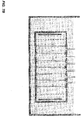
- Schematics of a 200 mm round and 165 mm square process chambers are shown in FIGS. 3A , 3B , and 4 . Each of those figures shows side view 200, closed sectional view 202, and open sectional view 204.
- the substrates involved may be essentially flat with varying degree of roughness or may be structured to form 3-dimensional patterns or structured with films that locally inhibit or enable porous silicon formation.
- the process chambers are envisioned to be able to open in multiple sections, like a clam shell as shown in FIGS. 3A , 3B , and 4 .
- This allows easy loading of a batch of wafers (n wafers at a time) when the upper portions of the chamber walls are open.
- the sides and top portion of the chamber close/ latch around the wafers. This creates a hermetic seal between the chamber wall and each individual wafer. This is extremely critical as the electric field from the electrodes on either end of the process chamber is required to pass through the wafers to form relatively uniform and repeatable porous silicon layers.
- the chamber of the square wafer can be installed with a wide variety of tilt from 0 degree (as shown in FIG. 3A ) to 45 degree (as shown in FIG. 3B ).
- the wide range of tilt or wafer orientation allows for the choice of optimal chemical flow and gas escape during the anodization process.
- a key requirement of the porous silicon process is to get substantially uniform porous silicon coverage on the full surface of the wafer, in some embodiments without any edge exclusions. This requires that no areas of wafer edge should be blocked or covered by any material that will prevent uniform electric field distribution and direct contact with the chemistry.
- One embodiment covers designs of mechanical features that can hold the wafer in place, but with zero to negligible contact points and blocking points on the wafer. As shown in FIG. 2 , a simple clamp type wafer holder may be used to enable this capability. An enlarged image of the wafer holder is shown in FIG. 5 . Wafer clamp 206 lacks this desirable property, preventing the formation of PS around the edge of the wafer.
- the chamber walls will be lined with either a single layer of chemically inert (HF and organic resistant) insulating rubber or foam to provide a leak-free seal between the wafer edge and the chamber wall or the wafer holders. This is critical to prevent any chemical leak or electric field leakage in areas where the clam shell chamber walls lock.
- HF and organic resistant chemically inert
- the batch chamber design with the compartmentalized electrode chamber allows for electric modulation as well.
- the parameters such as electrode dimension, gap between electrode and closest wafer, gap from wafer to wafer, etc. may easily be modified to achieve the required uniformity for the electric field.
- Another key component is the spacers used to hold the membrane discussed above.
- the shape and patterns on the insulating spacer may also be modified to achieve the best electric field uniformity on the wafer. In circumstances where a varying electric field (thereby varying thickness or porosity of porous silicon) is required for the integrated process flow, the spacer design can be used to control the required electric field without changing the chamber design.
- the chamber may be designed with fluid fill and vent ports 208 on the top of the chamber as shown in FIG. 6 . As shown, this embodiment also includes designs of fluid inlet and outlet ports at other locations of the chamber to achieve the best electrolyte replenishment to the wafer (to minimize the impact of reaction byproducts) and maintain a consistent chemical concentration.
- H 2 hydrogen
- Hydrogen evolves from the surface of the wafer and each electrode. Since the bath is integral with electrical current transmission, H 2 gas blocks current flow and supply of chemicals to the reaction surface, thus affecting porous silicon formation and continuity/uniformity. It is therefore critical to effectively and rapidly purge or sweep H 2 byproducts from the surfaces of the wafer and electrodes.
- the wafer gap, fluid flow and design of the flow ports determine the effectiveness of the sweep. While sweeping H 2 is fairly simple in terms of fluid mechanics, some consideration is warranted to mitigate the current loss from the fluid ports.
- the fluid lines are connected from wafer to wafer, depending on the geometry of the ports, line size and length, current can leak or bypass each wafer. Therefore, isolation of each port is advantageous. Also, for example, reducing the line diameter and increasing the length results in greater electrical resistance which reduces current losses or bypass losses.
- the current field lines are also influenced by the geometry adjacent to the wafer. So, large flow ports are less desirable compared to multiple small ports.
- Typical wet chemical baths and process chambers use direct fluid fill/drain of the process chamber, wherein the chemical is directly pumped in the process chamber. This may require additional fill and drain times before the process can start and results in loss of productivity.
- This embodiment also covers a design termed as "bath in bath” for the PS production as shown in FIGS. 7A and 7B .
- this bath in bath design There are at least two embodiments of this bath in bath design: a) Prefilled inner chamber that is immersed and lifted out completely into and from the bath; b) Resident bath-in-bath with wafers being handled using auto loader that handles a batch of wafers and that places the batch into the lower holder part of the inside bath, then retreats.
- the process chamber is pre-loaded with wafers and filled with the process chemicals.
- the entire assembly is then immersed into a larger bath which is pre-filled with the process chemical/electrolyte.
- the ports/vents on the top of the chamber allow for the electrolyte to fill the process chamber if and when the liquid level drops in the process chamber due to the reaction or other means of loss such as evaporation.
- the process chamber unlocks and is pulled out and the standby process chamber is immediately immersed in the larger bath minimizing loss in productivity due to wafer load/unload and chamber fill and drain.
- the larger bath is designed with its own pumping and recirculation system to maintain the required concentration and temperature. This methodology allows having multiple process chambers that can be introduced into the main bath without any loss in productivity.
- the chamber is an integral part of the tool or the larger bath and always remains immersed in the main bath, but the chamber can open and close. It is envisioned that loading mechanisms such as robotic handlers can transfer a batch of n wafers into the base of the process chamber. After the wafer handlers have moved away from the process chamber, the outer walls of the process chamber close. This action not only secures the wafers, but also encloses the process chemicals in to the process chamber. The additional vents and ports allow the process chamber to be filled completely to the required level and maintain the same level throughout the process.
- loading mechanisms such as robotic handlers can transfer a batch of n wafers into the base of the process chamber. After the wafer handlers have moved away from the process chamber, the outer walls of the process chamber close. This action not only secures the wafers, but also encloses the process chemicals in to the process chamber.
- the additional vents and ports allow the process chamber to be filled completely to the required level and maintain the same level throughout the process.
- the top of the vent ports may be outside of the liquid, such that an electrically connecting path outside of the inner bath is avoided. This embodiment is shown in FIG. 7B .
- design a) and design b) can be combined into a hybrid utilizing the loading mechanism from design a) and the sealing mechanism from design b).
- the bottom section of the chamber remains in the outer bath.
- the wafers are pre-loaded into the top (and side) portion of the chamber, which acts both as a handling mechanism and a partial chamber.
- the preloaded wafers are then immersed in the outer bath until the wafers make contact with the lower portion of the chamber.
- the chamber walls are then closed tight with an actuator mechanism ensuring a leak-proof chamber.
- the batch porous silicon equipment design embodiments described above can be used to form either single-layer or multi-layer porous silicon on one or both sides of the wafers in the batch.
- Porous silicon can be formed on only one side of the wafers by applying the electrical current flowing in only one direction without a change in the current polarity.
- porous silicon can be formed on both sides of the wafers by alternating the current flow direction at least once or multiple times.
- the electrical current density controls the layer porosity.
- the layer porosity can be increased by increasing the electrical current density and conversely can be reduced by reducing the electrical current density.
- Multi-layer porous silicon can be formed by modulating or changing the electrical current level in time during the porous silicon formation process.
- a graded porosity porous silicon layer may be formed by, for instance, linearly modulating or varying the electrical current density in time.
- FIGS. 8-16B and the following corresponding description relate more directly to the subject matter disclosed in the present application which provides process flows, unit processes, apparatuses, and variations thereof which enable the controlled formation of one or more uniform layers of porous semiconductor or silicon (PS) on top of semiconductor or silicon templates.
- These processes and apparatuses allow for the controlled formation of uniform layer or layers of porous silicon (PS) in a batch mode - which means the formation of PS on a plurality of wafers at the same time with substantially uniform distribution of porosity and thickness of the PS layers.
- a key factor in the uniform anodization of a wafer surface in a bath reactor is the suppression and minimization of the quantity, density, and impact of gas bubbles formed during the anodization process.
- an etching fluid consisting of HF and typically an additive, such as an alcohol, to reduce the surface tension
- a byproduct of the reaction is the liberation of gas bubbles, substantially hydrogen gas bubbles.
- hydrogen bubbles tend to accumulate towards the top of the reaction chamber as the bubbles move towards the surface of the etching fluid.
- the effect of these bubbles may cause non-uniform anodization at the top of the wafer, or even blistering of layers, especially when forming a low porosity layer over higher porosity layer on the wafer surface.
- One disclosed solution employs the use of sonic energy, such as ultrasonic or megasonic transducers coupled to the fluid bath or to the wafer holder, to effectively dislodge and liberate such bubbles from the surface.
- sonic energy such as ultrasonic or megasonic transducers coupled to the fluid bath or to the wafer holder
- Another disclosed solution utilizes pulsed anodization - the current is pulsed on and off as shown in the graph in FIG. 8 - where the formation of the anodization is pulsed to give the hydrogen bubbles that are formed during the reaction sufficient time to travel up and away through a vent hole, or a plurality of vent holes, at the top or along the upper edges of the chamber or wafer tunnel.
- the bubbles may also be swept away by an upwards chemical flow. It is to be noted that the formation of a high porosity layer is typically accomplished at a substantially higher electrical current than the formation of a low porosity layer.
- the anodization speed in terms of anodizing a certain thickness of film, increases with the current (i.e., higher porosity films form faster than lower porosity films). Therefore, high porosity films typically take less time to form but generate more hydrogen per unit time, making the formation of higher porosity films susceptible to hydrogen bubble-induced uniformity problems. Thus, if a plurality of layers with at least one lower porosity layer is formed, the throughput loss from forming the high porosity layer in a pulsed fashion is comparatively minor.
- a third disclosed embodiment utilizes fluid transport to dislodge gas bubbles while the anodization is in an off-state.
- an active fluid transport which sweeps the hydrogen gas away may be turned on - the fluid transport is left turned off during the anodization.
- This method may be beneficial to the uniformity of the electrical field, as a moving electrolyte tends to carry electrical field lines with it and can cause field distortions.
- suitably directed fluid flow during the anodization may also be utilized to create a uniform overall anodization result.
- proper care needs to be taken to avoid contact of fluid volumes from the different fluid compartments between wafers.
- An exemplary system that may be used to push liquid through the reactor are separate tubes connected to the bottom of each compartment. Through these tubes, the liquid is pushed across the wafers thus displacing other liquid and bubbles through the vent holes on the upper part of the chamber.
- One skilled in the art may envision various methods and systems for keeping the replenishing fluids as well as the displaced fluids between individual compartments separated.
- Yet another alternative method for bubble removal utilizes a suitable vacuum, which may be for instance applied to the vent holes of the anodization chamber.
- the electrical power dissipation per wafer in the batch porous silicon tool may be reduced by adding a suitable additive such as a salt or an acid to the anodization bath in order to enhance its electrical conductivity without any detrimental impact on the anodization chemistry and process.
- a suitable additive such as a salt or an acid
- An increase in the electrical conductivity of the batch porous silicon bath through a suitable conductivity-enhancement additive such as a chemically-benign salt or acid not only reduces the electrical power dissipation per wafer but also enables an increase in the wafer batch size by reducing the wafer-to-wafer spacing within the bath.
- the reduction in wafer-to-wafer spacing may be achieved because it is possible within a more conductive electrolyte to equalize the electric field strength across a smaller distance - thus enabling smaller wafer-to-wafer compartments and allowing for an increase in wafer batch size.
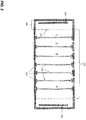
- Figure 9 is a diagram depicting an embodiment of stacked batch anodizing tool 300.
- Key components of the tool include anode 306 and cathode 308 (both facing the wafers), and wafer chamber 302 supporting an n-dimensional array of wafers, such as wafer 312 through 314, held in place by wafer clamps 316 in electrolyte solution 310 filled in the compartment to height 328.
- Vent holes 304 provide access to each fluid filled wafer compartment created between two wafers positioned in series.
- Anode 306, having electrode region size 318, is positioned a certain distance from the wafer chamber, shown as distance 320, and the first wafer, wafer 312 , is positioned a certain distance from the beginning of the wafer chamber, shown as field shaping distance 324.
- Seals 332 define the wafer tunnel and help to prevent additional current paths between the electrodes other than that within the tunnel and through the wafers.
- the wafer tunnel has height 322 (also called tunnel size) and each fluid filled compartment between two wafers has width 326 and height (also called compartment size and compartment size diameter) 330.
- the diameter of the space between wafers mimics the wafer size, i.e. if the wafers were round or square with a certain diameter or diagonal, it is beneficial to have the diameter of the space between the wafers, called the compartment size and shown as width 330 in FIG. 9 , approach similar dimensions.
- the same distance parameters also hold in general between the first wafer, wafer 312, and the anode and last wafer, wafer 314, and the cathode. Therefore, a 'tunnel' arrangement between the electrode and the first wafer with a similar height dimension to the wafer itself, shown as tunnel size 322 in FIG. 9 , is employed to help provide improved uniformity.
- the diameter of the compartment size be slightly larger than the wafer diameter.
- a compartment size 330 larger than the size of the wafer, while connected to the vent hole or holes, allows for bubbles to be temporarily stored during the anodization without being in the direct path of the anodization current.
- Another consideration is that in the case that the sealing at the wafer edge is asymmetric, as is described below, the additional fluid space between wafers allows the electric field to equalize towards the wafer edge.
- the tunnel pieces between electrodes and first and last wafers also resemble a similar shape and size as the wafers - in FIG. 9 this shown as the area having width 324 and height 322 between the electrode and wafer 312.
- the tunnel dimensions, width 324 and height 322, are called “field shaping tunnel distance” and “tunnel size” respectively.
- Tunnel size 322 should be substantially similar to wafer size and tunnel distance 324 is preferably large enough to form a homogenized uniform electric field across the wafer. And often a larger field shaping tunnel distance is advantageous.
- the dimension called “electrode region size", shown as 318 in FIG. 9 is kept similar to the tunnel size and wafer size.
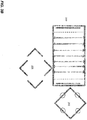
- FIGS. 10 through 12 are diagrams depicting several embodiments of a stacked batch anodizing tool highlighting various electrode positions. The structural features depicted in the diagrams of FIGS. 10 through 12 are consistent with FIG. 9 unless otherwise noted.
- Electrodes that are chemically very inert. Such electrodes tend to be costly which increases substantially with the electrodes size. Therefore, to decrease the overall tool cost it is advantageous to have small electrodes and utilize suitable field shaping to optimally expand the electric field and provide a uniform electric field for the anodization.
- the electrode may be placed at a larger distance from the first and/or last wafer in order to make use of the electrolyte's conductivity to distribute the field evenly - thus increasing/adjusting the distances 320 and 324 in FIG.9 .
- small anode 340 and small cathode 342 have been positioned further from the first and last wafers to allow for electric field homogenization before the first wafers are reached, the field is shown in FIG. 10 as field lines 344.
- the distances 346 and 348 combined are larger than distances 320 and 324 in FIG. 9 .
- additional electric field improvement may also be achieved by adding a conductivity-enhancement additive such as a suitable salt or acid to the anodization bath.
- anode 306 and cathode 308 face inwards, or towards the wafers. However, to expand the electric field the electrode may be positioned facing away from the wafers to be anodized - as shown in FIGS 11 and 12 .
- small anode 350 and small cathode 352 are facing outwards, or away from the wafers.
- This geometry, where the electric field generated by the electrode faces away from the wafer can be advantageous, since the field lines, shown as field lines 354, can be shaped readily by the shape of the surrounding tunnel walls.
- the backside wall of the electrode may be shaped to optimized the field shape effectiveness at a minimized distance to the first wafer. This may also help to reduce the ohmic loss due to the voltage drop in the electrolyte, as the electrolyte distance from the electrode to the first wafer plays a large role in the total ohmic loss and therefore electricity consumption of the anodization array.
- a wall may be shaped in a vertical wafer stack arrangement (where wafers are arranged vertically as shown in FIGS. 9-12 ) or in a horizontal wafer stack arrangement. In the case of a horizontal wafer stack arrangement, a pre-shaped (dome-shaped) wall above the electrode may likely require one or several perforations to avoid trapping gas underneath the dome.
- the liquid spaces between wafers are essentially compartmentalized by the wafers themselves and seals at the edge of the wafers (wafer clamps 316 in FIG . 9 ).
- FIG. 13A is a diagram of symmetric wafer seal 402 holding wafer 400.
- Seal 402 is applied centrally to the bevel apex of wafer 402 and provides both sealing and clamping of the wafer.
- the sealing material should be optimized to keep the seal extent as close to the bevel apex as possible to keep the sealing material from excessively wrapping around the wafer edge. Clamping may be performed, for example, by exerting clamping forces by means of a flexible seal to the edge of the wafer, substantially with a force in plane with the wafer plane and vertical to the bevel apex.
- wafer surface areas close to the bevel apex such as area 404 in FIG. 13 , may not receive proper anodization, since the anodization requires that liquid be directly in touch with the surface to be anodized.
- the seal must both eliminate fluid leakage around the edge of the wafer and at the same time minimally affect the anodization of the wafer.
- the wraparound of the sealing material around the bevel needs to be minimized, as said wraparound prevents areas contacted by the flexible seal from being anodized, while also performing a fluid tight seal.
- a disclosed solution to the optimization problem stated above and depicted in FIG. 13B includes the use of a seal or sealing arrangement with layers of more than one softness.
- wafer 406 clamped by layer 408, called in inner seal layer which is soft and has a limited thickness such that the wraparound is limited.
- the next layer, backing layer 409 or outside layer has a higher hardness while still allowing for long range flexibility.
- the backing layer still allows for adjustments needed to seal adjacent wafers with slightly differing diameters, and the wafer edge wraparound is optimized for perfect sealing while obstructing only a very small part of the bevel.
- This layer system may be comprised of several material sheets or of one material sheet with a graded softness. Further, this solution would work equally well for single sided and double sided anodization.
- FIG. 14A is a diagram of asymmetric wafer seal 410 holding the backside edge of wafer 418.
- Asymmetric wafer seal 410 may be utilized in a similar manner to the wafer clamps 316 in stacked batch anodizing tool 300 of FIG. 9 .
- Small slanted pin 412 presses the wafer towards flexible seal contact 414 and only contacts a minimal portion of the waver bevel, shown as contact bevel area 420.
- Seal holder 416 supports seal contact 414 and pin 412 and may be integrated into the bath chamber wall and allow for suitable electric field shaping geometry (see FIG. 15 ).
- the fluid filled compartment between each wafer is sealed by seal contact 414, which is a flexible and chemically resistant material such as, for example, a thermoplastic fluoropolymer (i.e. Polyvinylidene Fluoride PVDF foam), and is positioned substantially along on the backside edge of each wafer.
- a thermoplastic fluoropolymer i.e. Polyvinylidene Fluoride PVDF foam
- FIG. 14B is a front view, in the direction of the electric field, of asymmetric wafer seal 410 of FIG. 14A holding wafer 418 using slanted pins 412 that touch the front side bevel of the wafer without touching the flat surface area of the wafer - thus providing an asymmetric ring seal (the ring being round or square or pseudo-square, depending on the substrate geometry).
- the pins may be actuated (active) pins or passive pins wherein the holding force is essentially generated by the elasticity of the seal and/or by flexing of the pins.
- FIG. 15 is a diagram illustrating the shaping of the electric field, shown by filed lines 422, in the region of asymmetric seal 410 of FIG. 14 during anodization using a tool such as the stacked batch anodizing tool 300 of FIG. 9 .
- the electric field is reshaped and substantially uniform at each wafer front surface. It is to be noted that one direction of the electric field is depicted in FIG. 15 , however, the same holds for current and field pointing in the opposite direction, as is the case for frontside anodization.
- ring seal 414 positioned at the backside edge of the wafer is to have a sufficiently large extension to accommodate for a change or variation of wafer diameter or thickness as a function of the re-use of the wafer.
- the ring seal will typically have a shape substantially similar to the wafer itself, such as circular for a round wafer, square for a square wafer and so on.
- the small slanted pins may be replaced by a continuous and suitably slanted wedge.
- FIG. 16A and 16B are diagrams depicting an alternative asymmetric seal embodiment.
- FIG. 16A is a diagram of asymmetric wafer seal 440 holding the backside edge of wafer 448.
- Asymmetric wafer seal 440 may be utilized in a similar manner to the wafer clamps 316 in stacked batch anodizing tool 300 of FIG. 9 .
- Wafer 448 is held in place by small pin 442 which presses onto porous material 450.
- Porous material 450 is a suitably soft, sponge-like porous or nanoporous material fluid permeable material, such as PVA or other suitable compatible materials which let both the electric field as well as fluids pass through to the surface of the wafer.
- This same compressive force from pin 442 is used to press wafer 448 onto compressible seal 444 positioned on the back side of the wafer and which serves to isolate the fluid on one side of the wafer from the fluid on the other side of the wafer.
- Seal holder 446 supports compressible seal 444, pin 442, and porous material 450 and acts as a sealable ring similarly to seal holder 416 in FIG. 14 .
- the small slanted pins may be replaced by a continuous and suitably slanted wedge.
- Asymmetric wafer seal 440 is similar to asymmetric wafer seal 410 in FIG. 14 except for the addition of porous material 450 positioned along the circumference of the wafer and acts as a compressible sponge-like fluid permeable ring allowing electric field permeations and fluid to contact the front surface of the wafer. In this way, the extent of PS formation may be tuned and extended suitably towards and beyond the apex of the wafer bevel.
- the sponge-like material can extend past the edge area and across the whole wafer or large parts of the wafer.
- the fluid filled compartments between the wafers in a stacked batch anodizing tool, such as that of FIG. 9 , and optionally also the space between the electrodes and first or last wafer can be comprised fully of a sponge-like material - thus the wafer chamber of FIG. 9 is filled with a sponge-like material.
- the compressible sponge-like material may first be compressed, then relaxed to facilitate soaking up the etching chemistry prior to turning on the anodization current.
- the compressibility and the holding capacity of such a sponge/wafer/sponge/wafer array arrangement may be advantageously used to squeeze out bubbles of the gases developed by the reaction without the danger of generating connecting compartments with respect to electrical or fluid communication.
- This arrangement may also be used before, during, between or after anodization steps.
- the sponge like structure depending on the microscopic structure, may also serve to sufficiently retain the formed bubbles and keep them from accumulating towards the top of the bath where they may lead to non-uniform anodization.
- this sponge-like layer arrangement may be also used to facilitate easy centering of an edge or backside edge seal gasket between the compartments.
- All described arrangements and sealing systems and methods may be optimized by suitable choices of material and geometry that accommodate variations in wafer diameter, thickness, warpage, bevel form, and other shape variations in such a way that reliable sealing of the individual fluid compartments on each side of each wafer is achieved.
- the wafer holders are suitably segmented to allow for wafer loading and unloading which may be accomplished, for example, by segmenting the whole batch into a clamshell-like design with two or more segments for load and unload or by stacking individual wafer holders, similar to arrangements depicted in Figs 3A , 3B and 4 .
- the slanted pins may be passive, i.e. the pressure onto the wafer bevel is exerted just by the loading geometry, or also spring loaded or actuated to exert the necessary clamping pressure.
- this disclosure enables low cost, high-throughput fabrication of thin film (or thin crystalline semiconductor foil) substrates to be used for solar cell manufacturing by means of a preferably reusable template which can be used repeatedly to fabricate and release said thin film (or thin foil) crystalline semiconductor substrates.
- the application fields of this disclosure not only include solar photovoltaics, but also other semiconductor areas including microelectromechanical systems (MEMS) and optoelectronics.
- the field of the disclosure covers several apparatuses and methods for generating uniform layers or multilayers of porous semiconductor with controlled porosity profile across the porous layer (or multilayer) which then may be used as sacrificial release layers for removing a thin film semiconductor substrate deposited on top of a template with the release layer(s).
- Other applications of the porous semiconductor layers produced by the methods and apparatus of this invention include non-sacrificial applicators such as formation of anti-reflection coatings, optoelectronics, and layers for chemical sensors, etc.
Claims (16)
- Vorrichtung zur Herstellung von porösem Halbleiter auf einer Mehrzahl von Halbleiter-Wafern (312, 314), umfassend:eine elektrolytgefüllte Kammer, wobei die Kammer mehrere Abschnitte aufweist, die sich wie eine Muschelschale öffnen und schließen lassen und eine Dichtung bilden, wenn sie geschlossen sind;eine Anode (306), die an einem ersten Ende der Kammer angeordnet ist;eine Kathode (308), die an einem gegenüberliegenden Ende der Kammer angeordnet ist, wobei die Anode (306) und die Kathode an eine elektrische Schaltung gekoppelt sind, die in der Lage ist, elektrische Leistung einschließlich von elektrischer Spannung und elektrischem Strom liefern zu können;eine Aufstellung einer Mehrzahl von Halbleiter-Wafern (312, 314), die zwischen der Anode (306) und der Kathode (308) in einem Tunnel angeordnet sind, wobei jeder der Wafer durch eine Wafer-Klemme (316) gehalten ist, welche den Oberflächenrand des Wafers fixiert und den fluidgefüllten Zwischenraum, der zwischen jedem der Wafer und dem Tunnel gebildet ist, abdichtet;wobei die Anode (306) und die Kathode (308) eine Flächengröße haben, die kleiner ist als die diagonale Abmessung von dem Wafer (312, 314), wobei die Anode (306) und die Kathode (308) jeweils einer Rückwand (360) der Kammer zu- und von der Aufstellung der Mehrzahl von Halbleiter-Wafern abgewandt sind; undeine Mehrzahl von Entlüftungsabzügen (304) in der Kammer, um während der Anodisierung der Wafer (312, 314) entstehendes Nebenproduktgas entweichen zu lassen;wobei die Wafer-Klemme (316) eine erste innere Schicht für minimale Randumhüllung und eine zweite äußere weniger flexible Schicht aufweist, um eine Dichtung um den Wafer-Rand herum zu bilden.
- Vorrichtung nach Anspruch 1, wobei die Rückwände (360), die der Anode (306) und der Kathode (308) zugewandt sind, kuppelförmig geformt sind, um ein relativ uniformes elektrisches Feld zwischen der Anode (306) und der Kathode (308) zu schaffen.
- Vorrichtung nach Anspruch 1, die weiterhin Schallgeber umfasst, die in der elektrolytgefüllten Kammer angeordnet sind, um Nebenproduktgasblasen von der Oberfläche der Wafer mit Schallenergie zu entfernen.
- Vorrichtung nach Anspruch 3, wobei die Schallgeber an den Wafer-Klemmen (316) angeordnet sind.
- Vorrichtung nach Anspruch 1, wobei die elektrische Schaltung dazu eingerichtet ist, um einen elektrischen Strom zwischen einem eingeschalteten und ausgeschalteten Zustand für eine ausreichende Zeitdauer hin und her zu schalten, um Zeit zu schaffen für die Dissipation von Nebenproduktgas von der Oberfläche der Wafer durch pulsierenden elektrischen Strom während der Anodisierung.
- Vorrichtung zur Herstellung von porösem Halbleiter auf einer Mehrzahl von Halbleiter-Wafern (312, 314), umfassend:eine elektrolytgefüllte Kammer, wobei die Kammer mehrere Abschnitte aufweist, die sich wie eine Muschelschale öffnen und schließen lassen und eine Dichtung bilden, wenn sie geschlossen sind;eine Anode (306), die an einem ersten Ende der Kammer angeordnet ist;eine Kathode (308), die an einem gegenüberliegenden Ende der Kammer angeordnet ist, wobei die Anode (306) und die Kathode (308) an eine elektrischen Schaltung gekoppelt sind, die in der Lage ist, elektrische Leistung einschließlich von elektrischer Spannung und elektrischem Strom liefern zu können;eine Aufstellung einer Mehrzahl von Halbleiter-Wafern (312, 314), die zwischen der Anode (306) und der Kathode (308) in einem Tunnel angeordnet sind, wobei jeder der Wafer durch eine unsymmetrische Wafer-Klemme gehalten ist, welche den Oberflächenrand des Wafers fixiert und den fluidgefüllten Zwischenraum, der zwischen jedem der Wafer und dem Tunnel gebildet ist, abdichtet, wobei die unsymmetrische Wafer-Klemme einen Dichtungshalter (416) aufweist, der eine Dichtung zwischen dem Umfang des Wafer-Rands und dem Tunnel bereit stellt, wobei der Dichtungshalter (416) eine Mehrzahl von Stiften (412) trägt, die Druck auf einen minimalen Bereich der abgeschrägten Oberfläche der anodisierten Seite des Wafers ausüben und den Wafer auf einem rückseitigen flexiblen Dichtungskontaktmaterial abdichten; undeine Mehrzahl von Entlüftungsöffnungen in der Kammer, um während der Anodisierung der Wafer entstehendes Nebenproduktgas entweichen zu lassen.
- Vorrichtung nach Anspruch 6, wobei die unsymmetrische Wafer-Klemme (416) außerdem ein poröses Material aufweist, das zwischen dem Stift (412) und der Oberfläche der anodisierten Seite des Wafers angeordnet ist, wobei das Material für ein Fluid und ein elektrisches Feld durchlässig ist.
- Vorrichtung nach Anspruch 7, wobei das poröse Material den fluidgefüllten Zwischenraum ausfüllt.
- Vorrichtung nach Anspruch 6, die weiterhin Schallgeber umfasst, die in der elektrolytgefüllten Kammer angeordnet sind, um Nebenproduktgas von der Oberfläche der Wafer mit Schallenergie zu entfernen.
- Vorrichtung nach Anspruch 9, wobei die Schallgeber an den Wafer-Klemmen (416) angeordnet sind.
- Vorrichtung nach Anspruch 6, wobei die elektrische Schaltung dazu eingerichtet ist, um einen elektrischen Strom zwischen einem eingeschalteten und ausgeschalteten Zustand für eine ausreichende Zeitdauer hin und her zu schalten, um Zeit zu schaffen für die Dissipation eines Nebenproduktgases von der Oberfläche der Wafer durch pulsierenden elektrischen Strom während der Anodisierung.
- Vorrichtung nach Anspruch 6, wobei das Nebenproduktgas Wasserstoffgas ist.
- Verfahren zum Bilden von porösem Halbleiter auf einer Mehrzahl von Halbleiter-Wafern, wobei das Verfahren umfasst:positionieren einer Mehrzahl von Wafern in einer Aufstellung in einer Vorrichtung, wobei die Vorrichtung umfasst:eine elektrolytgefüllte Kammer, wobei die Kammer mehrere Abschnitte aufweist, die sich wie eine Muschelschale öffnen und schließen lassen und eine Dichtung bilden, wenn sie geschlossen sind;eine Anode (306), die an einem ersten Ende der Kammer angeordnet ist;eine Kathode (308), die an einem gegenüberliegenden Ende der Kammer angeordnet ist, wobei die Anode und die Kathode an eine elektrische Schaltung gekoppelt sind, die in der Lage ist, elektrische Leistung einschließlich von elektrischer Spannung und elektrischem Strom liefern zu können;eine Mehrzahl von Halbleiter-Wafern, die zwischen der Anode und der Kathode angeordnet sind, wobei jeder Wafer von einer Wafer-Klemme gehalten ist, die um einen Umfang des Wafers herum angeordnet ist, wobei die Wafer-Klemme es gestattet, eine Vorder- und eine Rückseite des Wafers ganz dem Elektrolyt auszusetzen;eine Mehrzahl von Entlüftungsabzügen (304) in der Kammer, um entstehendes Nebenproduktgas entweichen zu lassen;
undanodisieren der Mehrzahl der Wafer gemäß eines gepulsten Anodisierungsvorgangs, wobei der Anodisierungsvorgang einen elektrischen Strom zwischen einem eingeschalteten und ausgeschalteten Zustand für eine ausreichende Zeitdauer hin und her schaltet, um Zeit zu schaffen für die Dissipation des Nebenproduktgases, das sich während der Anodisierung bildet. - Verfahren zum Bilden von porösem Halbleiter auf einer Mehrzahl von Halbleiter-Wafern nach Anspruch 13, wobei die Wafer-Klemme einen Dichtungshalter aufweist, der eine Dichtung zwischen dem Umfang des Wafer-Rands und der Kammer bereit stellt, wobei der Dichtungshalter eine Mehrzahl von Stiften trägt, die Druck auf einen minimalen Bereich der abgeschrägten Oberfläche der anodisierten Seite des Wafers ausüben und den Wafer an einem rückseitigen flexiblen Dichtungskontaktmaterial abdichten.
- Verfahren nach Anspruch 13, wobei die Halbleiter-Wafer kristalline Silizium-Wafer sind.
- Verfahren nach Anspruch 13, wobei das Nebenproduktgas Wasserstoffgas ist.
Applications Claiming Priority (3)
| Application Number | Priority Date | Filing Date | Title |
|---|---|---|---|
| US40994010P | 2010-11-03 | 2010-11-03 | |
| US13/244,466 US9076642B2 (en) | 2009-01-15 | 2011-09-24 | High-Throughput batch porous silicon manufacturing equipment design and processing methods |
| PCT/US2011/059177 WO2013126033A2 (en) | 2010-11-03 | 2011-11-03 | Apparatus and methods for uniformly forming porous semiconductor on a substrate |
Publications (3)
| Publication Number | Publication Date |
|---|---|
| EP2652774A2 EP2652774A2 (de) | 2013-10-23 |
| EP2652774A4 EP2652774A4 (de) | 2016-04-27 |
| EP2652774B1 true EP2652774B1 (de) | 2017-10-11 |
Family
ID=49006342
Family Applications (1)
| Application Number | Title | Priority Date | Filing Date |
|---|---|---|---|
| EP11876396.0A Not-in-force EP2652774B1 (de) | 2010-11-03 | 2011-11-03 | Vorrichtung und verfahren zur gleichmässigen herstellung poröser halbleiter auf einem substrat |
Country Status (3)
| Country | Link |
|---|---|
| EP (1) | EP2652774B1 (de) |
| KR (1) | KR20140061287A (de) |
| WO (1) | WO2013126033A2 (de) |
Families Citing this family (6)
| Publication number | Priority date | Publication date | Assignee | Title |
|---|---|---|---|---|
| US9076642B2 (en) | 2009-01-15 | 2015-07-07 | Solexel, Inc. | High-Throughput batch porous silicon manufacturing equipment design and processing methods |
| US8906218B2 (en) | 2010-05-05 | 2014-12-09 | Solexel, Inc. | Apparatus and methods for uniformly forming porous semiconductor on a substrate |
| US8241940B2 (en) | 2010-02-12 | 2012-08-14 | Solexel, Inc. | Double-sided reusable template for fabrication of semiconductor substrates for photovoltaic cell and microelectronics device manufacturing |
| US9217206B2 (en) * | 2013-09-27 | 2015-12-22 | Sunpower Corporation | Enhanced porosification |
| US20170243774A1 (en) * | 2014-09-04 | 2017-08-24 | Applied Materials, Inc. | Method and apparatus for forming porous silicon layers |
| US20170317225A1 (en) * | 2014-12-10 | 2017-11-02 | Applied Materials, Inc. | System and method for all wrap around porous silicon formation |
Family Cites Families (10)
| Publication number | Priority date | Publication date | Assignee | Title |
|---|---|---|---|---|
| JP3110178B2 (ja) * | 1992-11-09 | 2000-11-20 | キヤノン株式会社 | 半導体基板の作製方法及び陽極化成装置 |
| DE69312636T2 (de) * | 1992-11-09 | 1998-02-05 | Canon Kk | Anodisierungsapparat mit einer Trägervorrichtung für das zu behandelnde Substrat |
| US6197654B1 (en) * | 1998-08-21 | 2001-03-06 | Texas Instruments Incorporated | Lightly positively doped silicon wafer anodization process |
| US6417069B1 (en) * | 1999-03-25 | 2002-07-09 | Canon Kabushiki Kaisha | Substrate processing method and manufacturing method, and anodizing apparatus |
| JP2000277478A (ja) * | 1999-03-25 | 2000-10-06 | Canon Inc | 陽極化成装置、陽極化成システム、基板の処理装置及び処理方法、並びに基板の製造方法 |
| DE19914905A1 (de) * | 1999-04-01 | 2000-10-05 | Bosch Gmbh Robert | Elektrochemische Ätzanlage und Verfahren zur Ätzung eines Ätzkörpers |
| EP1057546A1 (de) * | 1999-06-01 | 2000-12-06 | Applied Materials, Inc. | Megaschallreinigungsvorrichtung |
| KR100563978B1 (ko) * | 2002-05-14 | 2006-03-29 | 마츠시다 덴코 가부시키가이샤 | 전기화학산화방법 |
| KR100465877B1 (ko) * | 2002-08-23 | 2005-01-13 | 삼성전자주식회사 | 반도체 식각 장치 |
| JP2012515453A (ja) * | 2009-01-15 | 2012-07-05 | ソレクセル、インコーポレイテッド | 多孔質シリコン電解エッチングシステム及び方法 |
-
2011
- 2011-11-03 WO PCT/US2011/059177 patent/WO2013126033A2/en active Application Filing
- 2011-11-03 KR KR1020137014255A patent/KR20140061287A/ko not_active Application Discontinuation
- 2011-11-03 EP EP11876396.0A patent/EP2652774B1/de not_active Not-in-force
Non-Patent Citations (1)
| Title |
|---|
| None * |
Also Published As
| Publication number | Publication date |
|---|---|
| EP2652774A2 (de) | 2013-10-23 |
| WO2013126033A3 (en) | 2013-10-17 |
| EP2652774A4 (de) | 2016-04-27 |
| WO2013126033A2 (en) | 2013-08-29 |
| KR20140061287A (ko) | 2014-05-21 |
Similar Documents
| Publication | Publication Date | Title |
|---|---|---|
| US10829864B2 (en) | Apparatus and methods for uniformly forming porous semiconductor on a substrate | |
| US9869031B2 (en) | High-productivity porous semiconductor manufacturing equipment | |
| EP2652774B1 (de) | Vorrichtung und verfahren zur gleichmässigen herstellung poröser halbleiter auf einem substrat | |
| US10138565B2 (en) | High-throughput batch porous silicon manufacturing equipment design and processing methods | |
| EP2387458B1 (de) | System und verfahren zur elektroätzung von porösem silizium | |
| US9401276B2 (en) | Apparatus for forming porous silicon layers on at least two surfaces of a plurality of silicon templates | |
| US20170243774A1 (en) | Method and apparatus for forming porous silicon layers | |
| KR101279353B1 (ko) | 플라즈마 발생장치 | |
| US9890465B2 (en) | Apparatus and methods for uniformly forming porous semiconductor on a substrate | |
| EP2619790B1 (de) | Entwurf einer ausrüstung zur herstellung von porösem silicium mit hohem durchsatz und verarbeitungsverfahren dafür | |
| US20170317225A1 (en) | System and method for all wrap around porous silicon formation | |
| JP2017017082A (ja) | ウェハ処理装置、ウェハカセット搬送装置、太陽電池用基板の製造方法 | |
| JPH06326084A (ja) | 陽極化成装置 |
Legal Events
| Date | Code | Title | Description |
|---|---|---|---|
| PUAI | Public reference made under article 153(3) epc to a published international application that has entered the european phase |
Free format text: ORIGINAL CODE: 0009012 |
|
| AK | Designated contracting states |
Kind code of ref document: A2 Designated state(s): AL AT BE BG CH CY CZ DE DK EE ES FI FR GB GR HR HU IE IS IT LI LT LU LV MC MK MT NL NO PL PT RO RS SE SI SK SM TR |
|
| AX | Request for extension of the european patent |
Extension state: BA ME |
|
| R17D | Deferred search report published (corrected) |
Effective date: 20131017 |
|
| 17P | Request for examination filed |
Effective date: 20131107 |
|
| RBV | Designated contracting states (corrected) |
Designated state(s): AL AT BE BG CH CY CZ DE DK EE ES FI FR GB GR HR HU IE IS IT LI LT LU LV MC MK MT NL NO PL PT RO RS SE SI SK SM TR |
|
| RIN1 | Information on inventor provided before grant (corrected) |
Inventor name: KRAMER, KARL-JOSEF Inventor name: TAMILMANI, SUBRAMANIAN Inventor name: MOSLEHI, MEHRDAD, M. Inventor name: KAMIAN, GEORGE Inventor name: ASH-JAEE, JAY Inventor name: YONEHARA, TAKAO |
|
| RIN1 | Information on inventor provided before grant (corrected) |
Inventor name: KRAMER, KARL-JOSEF Inventor name: KAMIAN, GEORGE Inventor name: ASH-JAEE, JAY Inventor name: MOSLEHI, MEHRDAD, M. Inventor name: YONEHARA, TAKAO Inventor name: TAMILMANI, SUBRAMANIAN |
|
| DAX | Request for extension of the european patent (deleted) | ||
| A4 | Supplementary search report drawn up and despatched |
Effective date: 20160330 |
|
| RIC1 | Information provided on ipc code assigned before grant |
Ipc: C25F 3/12 20060101ALI20160322BHEP Ipc: H01L 21/02 20060101ALI20160322BHEP Ipc: C25F 7/00 20060101ALI20160322BHEP Ipc: H01L 21/306 20060101AFI20160322BHEP |
|
| REG | Reference to a national code |
Ref country code: DE Ref legal event code: R079 Ref document number: 602011042418 Country of ref document: DE Free format text: PREVIOUS MAIN CLASS: H01L0021306300 Ipc: C25D0017000000 |
|
| GRAP | Despatch of communication of intention to grant a patent |
Free format text: ORIGINAL CODE: EPIDOSNIGR1 |
|
| STAA | Information on the status of an ep patent application or granted ep patent |
Free format text: STATUS: GRANT OF PATENT IS INTENDED |
|
| RIC1 | Information provided on ipc code assigned before grant |
Ipc: C25F 3/12 20060101ALI20170207BHEP Ipc: H01L 21/306 20060101ALI20170207BHEP Ipc: C25F 7/00 20060101ALI20170207BHEP Ipc: C25D 17/00 20060101AFI20170207BHEP |
|
| INTG | Intention to grant announced |
Effective date: 20170310 |
|
| GRAS | Grant fee paid |
Free format text: ORIGINAL CODE: EPIDOSNIGR3 |
|
| GRAA | (expected) grant |
Free format text: ORIGINAL CODE: 0009210 |
|
| STAA | Information on the status of an ep patent application or granted ep patent |
Free format text: STATUS: THE PATENT HAS BEEN GRANTED |
|
| AK | Designated contracting states |
Kind code of ref document: B1 Designated state(s): AL AT BE BG CH CY CZ DE DK EE ES FI FR GB GR HR HU IE IS IT LI LT LU LV MC MK MT NL NO PL PT RO RS SE SI SK SM TR |
|
| REG | Reference to a national code |
Ref country code: GB Ref legal event code: FG4D |
|
| REG | Reference to a national code |
Ref country code: CH Ref legal event code: EP |
|
| REG | Reference to a national code |
Ref country code: IE Ref legal event code: FG4D |
|
| REG | Reference to a national code |
Ref country code: AT Ref legal event code: REF Ref document number: 936105 Country of ref document: AT Kind code of ref document: T Effective date: 20171115 |
|
| REG | Reference to a national code |
Ref country code: DE Ref legal event code: R096 Ref document number: 602011042418 Country of ref document: DE |
|
| REG | Reference to a national code |
Ref country code: FR Ref legal event code: PLFP Year of fee payment: 7 |
|
| REG | Reference to a national code |
Ref country code: NL Ref legal event code: MP Effective date: 20171011 |
|
| REG | Reference to a national code |
Ref country code: LT Ref legal event code: MG4D |
|
| REG | Reference to a national code |
Ref country code: AT Ref legal event code: MK05 Ref document number: 936105 Country of ref document: AT Kind code of ref document: T Effective date: 20171011 |
|
| PG25 | Lapsed in a contracting state [announced via postgrant information from national office to epo] |
Ref country code: NL Free format text: LAPSE BECAUSE OF FAILURE TO SUBMIT A TRANSLATION OF THE DESCRIPTION OR TO PAY THE FEE WITHIN THE PRESCRIBED TIME-LIMIT Effective date: 20171011 |
|
| PG25 | Lapsed in a contracting state [announced via postgrant information from national office to epo] |
Ref country code: FI Free format text: LAPSE BECAUSE OF FAILURE TO SUBMIT A TRANSLATION OF THE DESCRIPTION OR TO PAY THE FEE WITHIN THE PRESCRIBED TIME-LIMIT Effective date: 20171011 Ref country code: SE Free format text: LAPSE BECAUSE OF FAILURE TO SUBMIT A TRANSLATION OF THE DESCRIPTION OR TO PAY THE FEE WITHIN THE PRESCRIBED TIME-LIMIT Effective date: 20171011 Ref country code: NO Free format text: LAPSE BECAUSE OF FAILURE TO SUBMIT A TRANSLATION OF THE DESCRIPTION OR TO PAY THE FEE WITHIN THE PRESCRIBED TIME-LIMIT Effective date: 20180111 Ref country code: ES Free format text: LAPSE BECAUSE OF FAILURE TO SUBMIT A TRANSLATION OF THE DESCRIPTION OR TO PAY THE FEE WITHIN THE PRESCRIBED TIME-LIMIT Effective date: 20171011 Ref country code: LT Free format text: LAPSE BECAUSE OF FAILURE TO SUBMIT A TRANSLATION OF THE DESCRIPTION OR TO PAY THE FEE WITHIN THE PRESCRIBED TIME-LIMIT Effective date: 20171011 |
|
| PG25 | Lapsed in a contracting state [announced via postgrant information from national office to epo] |
Ref country code: IS Free format text: LAPSE BECAUSE OF FAILURE TO SUBMIT A TRANSLATION OF THE DESCRIPTION OR TO PAY THE FEE WITHIN THE PRESCRIBED TIME-LIMIT Effective date: 20180211 Ref country code: RS Free format text: LAPSE BECAUSE OF FAILURE TO SUBMIT A TRANSLATION OF THE DESCRIPTION OR TO PAY THE FEE WITHIN THE PRESCRIBED TIME-LIMIT Effective date: 20171011 Ref country code: HR Free format text: LAPSE BECAUSE OF FAILURE TO SUBMIT A TRANSLATION OF THE DESCRIPTION OR TO PAY THE FEE WITHIN THE PRESCRIBED TIME-LIMIT Effective date: 20171011 Ref country code: GR Free format text: LAPSE BECAUSE OF FAILURE TO SUBMIT A TRANSLATION OF THE DESCRIPTION OR TO PAY THE FEE WITHIN THE PRESCRIBED TIME-LIMIT Effective date: 20180112 Ref country code: BG Free format text: LAPSE BECAUSE OF FAILURE TO SUBMIT A TRANSLATION OF THE DESCRIPTION OR TO PAY THE FEE WITHIN THE PRESCRIBED TIME-LIMIT Effective date: 20180111 Ref country code: LV Free format text: LAPSE BECAUSE OF FAILURE TO SUBMIT A TRANSLATION OF THE DESCRIPTION OR TO PAY THE FEE WITHIN THE PRESCRIBED TIME-LIMIT Effective date: 20171011 Ref country code: AT Free format text: LAPSE BECAUSE OF FAILURE TO SUBMIT A TRANSLATION OF THE DESCRIPTION OR TO PAY THE FEE WITHIN THE PRESCRIBED TIME-LIMIT Effective date: 20171011 |
|
| REG | Reference to a national code |
Ref country code: DE Ref legal event code: R097 Ref document number: 602011042418 Country of ref document: DE |
|
| PG25 | Lapsed in a contracting state [announced via postgrant information from national office to epo] |
Ref country code: MC Free format text: LAPSE BECAUSE OF FAILURE TO SUBMIT A TRANSLATION OF THE DESCRIPTION OR TO PAY THE FEE WITHIN THE PRESCRIBED TIME-LIMIT Effective date: 20171011 Ref country code: LI Free format text: LAPSE BECAUSE OF NON-PAYMENT OF DUE FEES Effective date: 20171130 Ref country code: SK Free format text: LAPSE BECAUSE OF FAILURE TO SUBMIT A TRANSLATION OF THE DESCRIPTION OR TO PAY THE FEE WITHIN THE PRESCRIBED TIME-LIMIT Effective date: 20171011 Ref country code: CH Free format text: LAPSE BECAUSE OF NON-PAYMENT OF DUE FEES Effective date: 20171130 Ref country code: DK Free format text: LAPSE BECAUSE OF FAILURE TO SUBMIT A TRANSLATION OF THE DESCRIPTION OR TO PAY THE FEE WITHIN THE PRESCRIBED TIME-LIMIT Effective date: 20171011 Ref country code: CZ Free format text: LAPSE BECAUSE OF FAILURE TO SUBMIT A TRANSLATION OF THE DESCRIPTION OR TO PAY THE FEE WITHIN THE PRESCRIBED TIME-LIMIT Effective date: 20171011 Ref country code: EE Free format text: LAPSE BECAUSE OF FAILURE TO SUBMIT A TRANSLATION OF THE DESCRIPTION OR TO PAY THE FEE WITHIN THE PRESCRIBED TIME-LIMIT Effective date: 20171011 |
|
| PLBE | No opposition filed within time limit |
Free format text: ORIGINAL CODE: 0009261 |
|
| STAA | Information on the status of an ep patent application or granted ep patent |
Free format text: STATUS: NO OPPOSITION FILED WITHIN TIME LIMIT |
|
| PG25 | Lapsed in a contracting state [announced via postgrant information from national office to epo] |
Ref country code: LU Free format text: LAPSE BECAUSE OF NON-PAYMENT OF DUE FEES Effective date: 20171103 Ref country code: SM Free format text: LAPSE BECAUSE OF FAILURE TO SUBMIT A TRANSLATION OF THE DESCRIPTION OR TO PAY THE FEE WITHIN THE PRESCRIBED TIME-LIMIT Effective date: 20171011 Ref country code: PL Free format text: LAPSE BECAUSE OF FAILURE TO SUBMIT A TRANSLATION OF THE DESCRIPTION OR TO PAY THE FEE WITHIN THE PRESCRIBED TIME-LIMIT Effective date: 20171011 Ref country code: RO Free format text: LAPSE BECAUSE OF FAILURE TO SUBMIT A TRANSLATION OF THE DESCRIPTION OR TO PAY THE FEE WITHIN THE PRESCRIBED TIME-LIMIT Effective date: 20171011 Ref country code: IT Free format text: LAPSE BECAUSE OF FAILURE TO SUBMIT A TRANSLATION OF THE DESCRIPTION OR TO PAY THE FEE WITHIN THE PRESCRIBED TIME-LIMIT Effective date: 20171011 |
|
| REG | Reference to a national code |
Ref country code: BE Ref legal event code: MM Effective date: 20171130 |
|
| REG | Reference to a national code |
Ref country code: IE Ref legal event code: MM4A |
|
| 26N | No opposition filed |
Effective date: 20180712 |
|
| PG25 | Lapsed in a contracting state [announced via postgrant information from national office to epo] |
Ref country code: MT Free format text: LAPSE BECAUSE OF NON-PAYMENT OF DUE FEES Effective date: 20171103 |
|
| PLAA | Information modified related to event that no opposition was filed |
Free format text: ORIGINAL CODE: 0009299DELT |
|
| PLBE | No opposition filed within time limit |
Free format text: ORIGINAL CODE: 0009261 |
|
| STAA | Information on the status of an ep patent application or granted ep patent |
Free format text: STATUS: NO OPPOSITION FILED WITHIN TIME LIMIT |
|
| REG | Reference to a national code |
Ref country code: FR Ref legal event code: PLFP Year of fee payment: 8 |
|
| PG25 | Lapsed in a contracting state [announced via postgrant information from national office to epo] |
Ref country code: IE Free format text: LAPSE BECAUSE OF NON-PAYMENT OF DUE FEES Effective date: 20171103 |
|
| R26N | No opposition filed (corrected) |
Effective date: 20180712 |
|
| RAP2 | Party data changed (patent owner data changed or rights of a patent transferred) |
Owner name: TRUTAG TECHNOLOGIES, INC. |
|
| PG25 | Lapsed in a contracting state [announced via postgrant information from national office to epo] |
Ref country code: SI Free format text: LAPSE BECAUSE OF FAILURE TO SUBMIT A TRANSLATION OF THE DESCRIPTION OR TO PAY THE FEE WITHIN THE PRESCRIBED TIME-LIMIT Effective date: 20171011 Ref country code: BE Free format text: LAPSE BECAUSE OF NON-PAYMENT OF DUE FEES Effective date: 20171130 |
|
| PGFP | Annual fee paid to national office [announced via postgrant information from national office to epo] |
Ref country code: DE Payment date: 20181023 Year of fee payment: 8 |
|
| PGFP | Annual fee paid to national office [announced via postgrant information from national office to epo] |
Ref country code: FR Payment date: 20181024 Year of fee payment: 8 Ref country code: GB Payment date: 20181024 Year of fee payment: 8 |
|
| PG25 | Lapsed in a contracting state [announced via postgrant information from national office to epo] |
Ref country code: HU Free format text: LAPSE BECAUSE OF FAILURE TO SUBMIT A TRANSLATION OF THE DESCRIPTION OR TO PAY THE FEE WITHIN THE PRESCRIBED TIME-LIMIT; INVALID AB INITIO Effective date: 20111103 |
|
| PG25 | Lapsed in a contracting state [announced via postgrant information from national office to epo] |
Ref country code: CY Free format text: LAPSE BECAUSE OF NON-PAYMENT OF DUE FEES Effective date: 20171011 |
|
| PG25 | Lapsed in a contracting state [announced via postgrant information from national office to epo] |
Ref country code: MK Free format text: LAPSE BECAUSE OF FAILURE TO SUBMIT A TRANSLATION OF THE DESCRIPTION OR TO PAY THE FEE WITHIN THE PRESCRIBED TIME-LIMIT Effective date: 20171011 |
|
| PG25 | Lapsed in a contracting state [announced via postgrant information from national office to epo] |
Ref country code: TR Free format text: LAPSE BECAUSE OF FAILURE TO SUBMIT A TRANSLATION OF THE DESCRIPTION OR TO PAY THE FEE WITHIN THE PRESCRIBED TIME-LIMIT Effective date: 20171011 |
|
| PG25 | Lapsed in a contracting state [announced via postgrant information from national office to epo] |
Ref country code: PT Free format text: LAPSE BECAUSE OF FAILURE TO SUBMIT A TRANSLATION OF THE DESCRIPTION OR TO PAY THE FEE WITHIN THE PRESCRIBED TIME-LIMIT Effective date: 20171011 |
|
| REG | Reference to a national code |
Ref country code: DE Ref legal event code: R119 Ref document number: 602011042418 Country of ref document: DE |
|
| PG25 | Lapsed in a contracting state [announced via postgrant information from national office to epo] |
Ref country code: AL Free format text: LAPSE BECAUSE OF FAILURE TO SUBMIT A TRANSLATION OF THE DESCRIPTION OR TO PAY THE FEE WITHIN THE PRESCRIBED TIME-LIMIT Effective date: 20171011 |
|
| GBPC | Gb: european patent ceased through non-payment of renewal fee |
Effective date: 20191103 |
|
| PG25 | Lapsed in a contracting state [announced via postgrant information from national office to epo] |
Ref country code: FR Free format text: LAPSE BECAUSE OF NON-PAYMENT OF DUE FEES Effective date: 20191130 Ref country code: DE Free format text: LAPSE BECAUSE OF NON-PAYMENT OF DUE FEES Effective date: 20200603 Ref country code: GB Free format text: LAPSE BECAUSE OF NON-PAYMENT OF DUE FEES Effective date: 20191103 |
|
| P01 | Opt-out of the competence of the unified patent court (upc) registered |
Effective date: 20230605 |