EP2649005B1 - Verfahren zur herstellung von elektromechanischen systemen - Google Patents
Verfahren zur herstellung von elektromechanischen systemen Download PDFInfo
- Publication number
- EP2649005B1 EP2649005B1 EP10860616.1A EP10860616A EP2649005B1 EP 2649005 B1 EP2649005 B1 EP 2649005B1 EP 10860616 A EP10860616 A EP 10860616A EP 2649005 B1 EP2649005 B1 EP 2649005B1
- Authority
- EP
- European Patent Office
- Prior art keywords
- silicon nitride
- layer
- silicon
- substrate
- nems
- Prior art date
- Legal status (The legal status is an assumption and is not a legal conclusion. Google has not performed a legal analysis and makes no representation as to the accuracy of the status listed.)
- Active
Links
- 238000000034 method Methods 0.000 title claims description 34
- 238000004519 manufacturing process Methods 0.000 title claims description 14
- HQVNEWCFYHHQES-UHFFFAOYSA-N silicon nitride Chemical compound N12[Si]34N5[Si]62N3[Si]51N64 HQVNEWCFYHHQES-UHFFFAOYSA-N 0.000 claims description 58
- 229910052581 Si3N4 Inorganic materials 0.000 claims description 56
- 239000000758 substrate Substances 0.000 claims description 28
- LXPCOISGJFXEJE-UHFFFAOYSA-N oxifentorex Chemical compound C=1C=CC=CC=1C[N+](C)([O-])C(C)CC1=CC=CC=C1 LXPCOISGJFXEJE-UHFFFAOYSA-N 0.000 claims description 23
- KRHYYFGTRYWZRS-UHFFFAOYSA-N Fluorane Chemical compound F KRHYYFGTRYWZRS-UHFFFAOYSA-N 0.000 claims description 19
- 238000000859 sublimation Methods 0.000 claims description 18
- 230000008022 sublimation Effects 0.000 claims description 18
- VYPSYNLAJGMNEJ-UHFFFAOYSA-N Silicium dioxide Chemical compound O=[Si]=O VYPSYNLAJGMNEJ-UHFFFAOYSA-N 0.000 claims description 17
- 229910052814 silicon oxide Inorganic materials 0.000 claims description 15
- XLYOFNOQVPJJNP-UHFFFAOYSA-N water Substances O XLYOFNOQVPJJNP-UHFFFAOYSA-N 0.000 claims description 10
- RTAQQCXQSZGOHL-UHFFFAOYSA-N Titanium Chemical compound [Ti] RTAQQCXQSZGOHL-UHFFFAOYSA-N 0.000 claims description 6
- XAGFODPZIPBFFR-UHFFFAOYSA-N aluminium Chemical compound [Al] XAGFODPZIPBFFR-UHFFFAOYSA-N 0.000 claims description 6
- 229910052782 aluminium Inorganic materials 0.000 claims description 6
- 239000010936 titanium Substances 0.000 claims description 6
- 229910052719 titanium Inorganic materials 0.000 claims description 6
- WFKWXMTUELFFGS-UHFFFAOYSA-N tungsten Chemical compound [W] WFKWXMTUELFFGS-UHFFFAOYSA-N 0.000 claims description 6
- 239000010937 tungsten Substances 0.000 claims description 6
- 229910052721 tungsten Inorganic materials 0.000 claims description 6
- 238000000151 deposition Methods 0.000 claims description 5
- LFQSCWFLJHTTHZ-UHFFFAOYSA-N Ethanol Chemical compound CCO LFQSCWFLJHTTHZ-UHFFFAOYSA-N 0.000 claims description 4
- 238000001465 metallisation Methods 0.000 claims description 4
- 238000004806 packaging method and process Methods 0.000 claims description 4
- 229910000577 Silicon-germanium Inorganic materials 0.000 claims description 3
- NRTOMJZYCJJWKI-UHFFFAOYSA-N Titanium nitride Chemical compound [Ti]#N NRTOMJZYCJJWKI-UHFFFAOYSA-N 0.000 claims description 3
- LEVVHYCKPQWKOP-UHFFFAOYSA-N [Si].[Ge] Chemical compound [Si].[Ge] LEVVHYCKPQWKOP-UHFFFAOYSA-N 0.000 claims description 3
- 229910045601 alloy Inorganic materials 0.000 claims description 3
- 239000000956 alloy Substances 0.000 claims description 3
- 229910021417 amorphous silicon Inorganic materials 0.000 claims description 3
- 229910021420 polycrystalline silicon Inorganic materials 0.000 claims description 3
- 229920005591 polysilicon Polymers 0.000 claims description 3
- 230000015572 biosynthetic process Effects 0.000 claims description 2
- 239000007788 liquid Substances 0.000 claims description 2
- 238000004518 low pressure chemical vapour deposition Methods 0.000 claims 3
- 238000000623 plasma-assisted chemical vapour deposition Methods 0.000 claims 3
- 238000005530 etching Methods 0.000 description 15
- 150000004767 nitrides Chemical class 0.000 description 9
- QPJSUIGXIBEQAC-UHFFFAOYSA-N n-(2,4-dichloro-5-propan-2-yloxyphenyl)acetamide Chemical compound CC(C)OC1=CC(NC(C)=O)=C(Cl)C=C1Cl QPJSUIGXIBEQAC-UHFFFAOYSA-N 0.000 description 6
- 239000000463 material Substances 0.000 description 5
- 229940070337 ammonium silicofluoride Drugs 0.000 description 4
- QGZKDVFQNNGYKY-UHFFFAOYSA-N Ammonia Chemical compound N QGZKDVFQNNGYKY-UHFFFAOYSA-N 0.000 description 3
- -1 ammonium fluorosilicate Chemical compound 0.000 description 3
- 238000001039 wet etching Methods 0.000 description 3
- DDFHBQSCUXNBSA-UHFFFAOYSA-N 5-(5-carboxythiophen-2-yl)thiophene-2-carboxylic acid Chemical compound S1C(C(=O)O)=CC=C1C1=CC=C(C(O)=O)S1 DDFHBQSCUXNBSA-UHFFFAOYSA-N 0.000 description 2
- IJGRMHOSHXDMSA-UHFFFAOYSA-N Atomic nitrogen Chemical compound N#N IJGRMHOSHXDMSA-UHFFFAOYSA-N 0.000 description 2
- XUIMIQQOPSSXEZ-UHFFFAOYSA-N Silicon Chemical compound [Si] XUIMIQQOPSSXEZ-UHFFFAOYSA-N 0.000 description 2
- 229910052710 silicon Inorganic materials 0.000 description 2
- 239000010703 silicon Substances 0.000 description 2
- 239000000377 silicon dioxide Substances 0.000 description 2
- 239000011800 void material Substances 0.000 description 2
- 229910019975 (NH4)2SiF6 Inorganic materials 0.000 description 1
- QGZKDVFQNNGYKY-UHFFFAOYSA-O Ammonium Chemical compound [NH4+] QGZKDVFQNNGYKY-UHFFFAOYSA-O 0.000 description 1
- 229910017665 NH4HF2 Inorganic materials 0.000 description 1
- 229910004014 SiF4 Inorganic materials 0.000 description 1
- 229910004074 SiF6 Inorganic materials 0.000 description 1
- 230000001476 alcoholic effect Effects 0.000 description 1
- 238000005452 bending Methods 0.000 description 1
- 239000006227 byproduct Substances 0.000 description 1
- 229910052681 coesite Inorganic materials 0.000 description 1
- 229910052906 cristobalite Inorganic materials 0.000 description 1
- 230000009977 dual effect Effects 0.000 description 1
- 230000000694 effects Effects 0.000 description 1
- 238000005516 engineering process Methods 0.000 description 1
- 150000004673 fluoride salts Chemical class 0.000 description 1
- 230000004907 flux Effects 0.000 description 1
- 238000009472 formulation Methods 0.000 description 1
- 230000006870 function Effects 0.000 description 1
- 238000002955 isolation Methods 0.000 description 1
- 239000000203 mixture Substances 0.000 description 1
- 239000002071 nanotube Substances 0.000 description 1
- 229910052757 nitrogen Inorganic materials 0.000 description 1
- 238000000059 patterning Methods 0.000 description 1
- 239000000376 reactant Substances 0.000 description 1
- 150000003839 salts Chemical class 0.000 description 1
- 239000004065 semiconductor Substances 0.000 description 1
- 235000012239 silicon dioxide Nutrition 0.000 description 1
- ABTOQLMXBSRXSM-UHFFFAOYSA-N silicon tetrafluoride Chemical compound F[Si](F)(F)F ABTOQLMXBSRXSM-UHFFFAOYSA-N 0.000 description 1
- 229910052682 stishovite Inorganic materials 0.000 description 1
- 229910052905 tridymite Inorganic materials 0.000 description 1
Images


Classifications
-
- B—PERFORMING OPERATIONS; TRANSPORTING
- B81—MICROSTRUCTURAL TECHNOLOGY
- B81C—PROCESSES OR APPARATUS SPECIALLY ADAPTED FOR THE MANUFACTURE OR TREATMENT OF MICROSTRUCTURAL DEVICES OR SYSTEMS
- B81C1/00—Manufacture or treatment of devices or systems in or on a substrate
-
- B—PERFORMING OPERATIONS; TRANSPORTING
- B81—MICROSTRUCTURAL TECHNOLOGY
- B81C—PROCESSES OR APPARATUS SPECIALLY ADAPTED FOR THE MANUFACTURE OR TREATMENT OF MICROSTRUCTURAL DEVICES OR SYSTEMS
- B81C1/00—Manufacture or treatment of devices or systems in or on a substrate
- B81C1/00436—Shaping materials, i.e. techniques for structuring the substrate or the layers on the substrate
- B81C1/00523—Etching material
-
- B—PERFORMING OPERATIONS; TRANSPORTING
- B81—MICROSTRUCTURAL TECHNOLOGY
- B81B—MICROSTRUCTURAL DEVICES OR SYSTEMS, e.g. MICROMECHANICAL DEVICES
- B81B7/00—Microstructural systems; Auxiliary parts of microstructural devices or systems
- B81B7/02—Microstructural systems; Auxiliary parts of microstructural devices or systems containing distinct electrical or optical devices of particular relevance for their function, e.g. microelectro-mechanical systems [MEMS]
-
- B—PERFORMING OPERATIONS; TRANSPORTING
- B81—MICROSTRUCTURAL TECHNOLOGY
- B81C—PROCESSES OR APPARATUS SPECIALLY ADAPTED FOR THE MANUFACTURE OR TREATMENT OF MICROSTRUCTURAL DEVICES OR SYSTEMS
- B81C1/00—Manufacture or treatment of devices or systems in or on a substrate
- B81C1/00912—Treatments or methods for avoiding stiction of flexible or moving parts of MEMS
- B81C1/0092—For avoiding stiction during the manufacturing process of the device, e.g. during wet etching
- B81C1/00936—Releasing the movable structure without liquid etchant
-
- C—CHEMISTRY; METALLURGY
- C23—COATING METALLIC MATERIAL; COATING MATERIAL WITH METALLIC MATERIAL; CHEMICAL SURFACE TREATMENT; DIFFUSION TREATMENT OF METALLIC MATERIAL; COATING BY VACUUM EVAPORATION, BY SPUTTERING, BY ION IMPLANTATION OR BY CHEMICAL VAPOUR DEPOSITION, IN GENERAL; INHIBITING CORROSION OF METALLIC MATERIAL OR INCRUSTATION IN GENERAL
- C23C—COATING METALLIC MATERIAL; COATING MATERIAL WITH METALLIC MATERIAL; SURFACE TREATMENT OF METALLIC MATERIAL BY DIFFUSION INTO THE SURFACE, BY CHEMICAL CONVERSION OR SUBSTITUTION; COATING BY VACUUM EVAPORATION, BY SPUTTERING, BY ION IMPLANTATION OR BY CHEMICAL VAPOUR DEPOSITION, IN GENERAL
- C23C16/00—Chemical coating by decomposition of gaseous compounds, without leaving reaction products of surface material in the coating, i.e. chemical vapour deposition [CVD] processes
- C23C16/22—Chemical coating by decomposition of gaseous compounds, without leaving reaction products of surface material in the coating, i.e. chemical vapour deposition [CVD] processes characterised by the deposition of inorganic material, other than metallic material
- C23C16/30—Deposition of compounds, mixtures or solid solutions, e.g. borides, carbides, nitrides
- C23C16/40—Oxides
-
- C—CHEMISTRY; METALLURGY
- C23—COATING METALLIC MATERIAL; COATING MATERIAL WITH METALLIC MATERIAL; CHEMICAL SURFACE TREATMENT; DIFFUSION TREATMENT OF METALLIC MATERIAL; COATING BY VACUUM EVAPORATION, BY SPUTTERING, BY ION IMPLANTATION OR BY CHEMICAL VAPOUR DEPOSITION, IN GENERAL; INHIBITING CORROSION OF METALLIC MATERIAL OR INCRUSTATION IN GENERAL
- C23C—COATING METALLIC MATERIAL; COATING MATERIAL WITH METALLIC MATERIAL; SURFACE TREATMENT OF METALLIC MATERIAL BY DIFFUSION INTO THE SURFACE, BY CHEMICAL CONVERSION OR SUBSTITUTION; COATING BY VACUUM EVAPORATION, BY SPUTTERING, BY ION IMPLANTATION OR BY CHEMICAL VAPOUR DEPOSITION, IN GENERAL
- C23C16/00—Chemical coating by decomposition of gaseous compounds, without leaving reaction products of surface material in the coating, i.e. chemical vapour deposition [CVD] processes
- C23C16/44—Chemical coating by decomposition of gaseous compounds, without leaving reaction products of surface material in the coating, i.e. chemical vapour deposition [CVD] processes characterised by the method of coating
Definitions
- This invention relates to the field of manufacturing electro-mechanical systems which includes nano-electro-mechanical systems (NEMS) and micro-electro mechanical systems (MEMS). More particularly the invention relates methods of making MEMS and NEMS using vapour hydrofluoric etching.
- NEMS nano-electro-mechanical systems
- MEMS micro-electro mechanical systems
- NEMS are modern mechanical systems in which one of more of the mechanical elements are smaller than one micron in all directions.
- NEMS and the older technology MEMS are well known devices which consist of long thin beams that support large plates, all patterned on top of a sacrificial layer and anchored to the underlying substrate at one or more points. After the device is completed, the sacrificial layer is etched away and the plate and beams are free to move except at the anchor points.
- Mastrangelo U.S. Pat. 5,258,097 disclosed a method of fabricating microstructures on a silicon substrate by depositing a sacrificial layer which can be removed by wet etching techniques such as silicon dioxide. Void areas are formed in the sacrificial layer and then a column-forming layer, resistant to sacrificial layer etchant, is deposited through at least one hole to fill the void area and undercut areas which later provides support for the structural layer during wet etching of the remaining sacrificial layer.
- Dalsa Semicondutor discloses a method for making a MEMS device wherein anhydrous HF exposed silicon nitride is used as a temporary adhesion layer allowing the transfer of a layer from a Carrier Wafer to a Device Wafer.
- Won Ick Jang et al. discloses a fabrication of MEMS devices using anhydrous HF gas-phase etching with alcoholic vapour.
- a silicon nitride layer is provided between the substrate and a sacrificial oxide layer and/or between a device layer and the sacrificial oxide layer, and/or on a side of the device layer facing away from the sacrificial oxide layer, and converted to thicker ammonium hexafluorosilicate with vapor hydrofluoride (VHF) while simultaneously removing a portion of the sacrificial oxide.
- VHF vapor hydrofluoride
- ammonium hexafluorosilicate acts as a temporary support, shim, wedge, or tether which limits device movement during fabrication and is later removed by sublimation under heat and/or reduced pressure.
- the silicon nitride is not removed by sublimation until after one or more intermediate steps are conducted, the intermediate steps selected from dicing, packaging, and metallization, thereby preventing movement during the one or more intermediate steps.
- VHF etching is typically used as an improved method over wet etching for small MEMS or NEMS, especially when stiction is a concern. Stiction occurs when residual water on the surface(s) of two flat, small parts, pulls them in contact with each other where Van der Wals forces can then bind them. For large sacrificial oxide gaps (> 1 um) VHF process parameters like pressure, temperature and reactant ratios can aid in minimizing or eliminating the effects of stiction. However, when sacrificial oxide layers get very thin, and/or gaps between compliant features such as beams and springs become very narrow, as is the case with NEMS, there may be limitations to reducing water to a level that prevents stiction.
- VHF is made and introduced according to known formulations and methods and comprises hydrofluoric acid and alcohol or water.
- This invention exploits two unique phenomena that occur when using the VHF etch process on another standard semiconductor material, silicon nitride (Si 3 N 4 ). It is known that silicon nitride in the presence of VHF processing can react and be converted to ammonium fluoride [NH4]F and/or ammonium silicofluoride [NH4] 2 SiF 6 . These are fluoride salts and the converted layer of these salts tends to be thicker, having larger grain size than the starting silicon nitride material. The combined dual material film (ammonium silicofluoride over silicon nitride) grows in thickness when exposed to the etch process.
- This invention exploits both these phenomena to develop a novel method of securing moving parts of a device layer either during a VHF release or during any processing subsequent to the VHF release. This is accomplished by using one or more nitride layers, either adjacent to a or adjacent to sacrificial oxide layer or across two or more moving parts. In embodiments wherein the nitride layer is between the device and oxide layers and/or between the oxide and substrate layers, the nitride layer thickness is selected so that its final thickness, when converted, approximates, but does not completely fill, the gap between the device layer and the substrate after the sacrificial oxide layer has been etched.
- an additional nitride layer can be placed above the device layer to counteract the bending force of the nitride layer below the device layer as it is converted.
- the nitride layer is used as a tether above the device layer, the nitride converts to ammonium fluorosilicate and tethers beams, springs, or other parts of the device layer together so that they are not damaged during further processing.
- the device layer in some embodiments is comprised of areas which are designed to move in relation to each other or in relation to the substrate, wherein a silicon nitride layer is provided in the form of a tether to limit movement of the areas in relation to each other during fabrication, and wherein the silicon nitride tether is removed by sublimation when movement of the areas in relation to each other is permitted.
- the structure is then exposed to a vacuum bake at temperature and pressure conditions below the sublimation curve, thereby subliming the ammonium silicofluoride support structure so that the device is released with no water as part of the release process.
- the device layer can be any suitable material used in the art, including for example amorphous silicon, polysilicon, silicon-germanium, aluminum, tungsten, titanium, titanium nitride, alloys of aluminum, tungsten, and titanium, combinations thereof, and metal-silicon oxide stacks.
- MEMS microelectromechanical systems
- NEMS nanoelectro mechancical systems
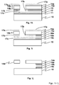
- FIG. 1a-1j an embodiment of an process according to the invention is illustrated wherein an NEMS stack is built and ultimately released in a series of steps.
- the starting substrate 10 is illustrated in Fig. 1a .
- One or more silicon nitride layers are deposited, depending on the embodiment.
- Fig. 1b illustrates a first silicon nitride layer 11, followed by deposit of a sacrificial oxide layer 12 ( Fig. 1c ), an intermediate silicon nitride layer 13 ( Fig. 1d ), a structure or device layer 14 ( Fig. 1e ), and a top nitride layer (Fig. If).
- the SiN layers are 20 nm (200 Angstroms) thick and the oxide layer is 50 nm (500 Angstroms) thick.
- the thickness of the structure or device layers can vary, even within a particular stack, as known in the art.
- the device layer 14 is 500 Angstroms thick.
- Fig. 1g illustrates a pattern being etched which divides layers 15, 14, and 13 into separate sections, 15a and 15b, 14a and 14b, and 13a and 13b, without etching the sacrificial oxide layer 12.
- Fig. 1h illustrates a the result of a partial VHF process release step which removes some sacrificial oxide 12 and simultaneously converts some of the silicon nitride, 11, 13a, 13b, 15a, 15b, into ammonium hexafluorosilicate 17a, 17b, 17c, or related chemistry which occupies greater volume than the silicon nitride which existed prior to the VHF step.
- the VHF comprises hydrofluoric acid (HF) and either alcohol or water vapor, and is introduced with nitrogen.
- the VHF step is conducted in this embodiment at 45°C and 13.3 kPa (100 Torr) but temperatures of about 20-100°C and pressures of 1.33 kPa (10 Torr) to atmospheric (101.3 kPa (760 Torr)) are suitable in other embodiments.
- the SiN layers 17b and 17c expand as they react with the HF to form ammonium hexafluorosilicate as the oxide layer is being removed until the expanded SiN/ammonium hexafluoriosilicate layers come in close proximity to each other so as to prevent the beam from collapsing onto the substrate due to stiction. Expanded SiN/ammonium hexafluorosilicate 17a serves to counteract any stress imparted by layer 17b as it forms.
- Fig. 1i illustrates the NEMS stack after a completed VHF release wherein ammonium hexafluorosilicate 17a supporting beams 14a and 14b from the top, ammonium hexafluorosilicate 17b is on the bottom of device layer 14a, 14b, and ammonium hexafluorosilicate 17c is on top of substrate 10.
- An anchor is formed from unreacted silicon nitride parts 16a and 16c and unreacted sacrificial oxide 16b.
- the anchor, 16a, 16b, 16c supports the device part 14a in this embodiment, and remains in place after the sublimation step which results in the final device stack illustrated in Fig. 1j.
- Fig. 1j shows the ammonium hexafluorosilicate 17a, 17b, and 17c having been removed by the sublimation step.
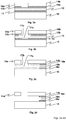
- Figs. 2a-2d are a series of cross-sectional views of an NEMS stack according to the invention illustrating the progression of VHF etching of a patterned NEMS stack which includes two silicon nitride layers 11 and 13a-13b, and a sublimation step.
- the patterned stack 2a is partially treated with VHF to convert a portion of each silicon nitride layer 11 and 13a-13b to expanded ammonium hexafluorosilicate 17b, 17c, and simultaneously remove a portion of the sacrificial oxide 12.
- Fig. 2c illustrates the stack after release and removal of all desired sacrificial oxide 12 ( Fig. 2a ), leaving the anchor for the beam 14b comprised of unreacted silicon nitride 16a, 16c, and unreacted sacrificial oxide 16b.
- the beam 14b is no longer supported and is now free to move as designed.
- Fig. 3a-3d illustrate a stack with only one silicon nitride layer 11.
- a patterned device layer in Fig. 3a results in a beam 14b and another member 14a in a device layer, supported by a sacrificial oxide layer 12, which is deposited after the silicon nitride layer 11 on top of the starting substrate 10.
- Fig. 3b shows the result of partial VHF release
- Fig. 3c show a completed VHF release with the anchor comprises of unreacted silicon nitride 16b and unreacted oxide 16a, wherein ammonium hexafluorosilicate 17 which is the expanded form of the silicon nitride supporting the beam 14b and member 14a.
- the ammonium hexafluorosilicate is removed anhydrously in the sublimation step resulting in a fully released NEMS device shown in Fig. 3d .
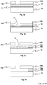
- Figs. 4a-4d illustrate another embodiment of the invention wherein a silicon nitride strip 15 is deposited over a pre-patterned device layer 13 in order to secure sections of the device layer 13 during the vapor HF release step.
- the silicon nitride 15 is converted to ammonium hexafluorosilicate 17 and portions of the sacrificial oxide 12 are removed during the VHF treatment step, resulting in an intermediate stack shown in Fig. 4b .
- a designed portion of sacrificial oxide 12 in Fig. 4c is not removed and functions as an anchor 16 which supports the sections or members 13 of the device layer in the final device after sublimation as shown in Fig. 4d .
- Figs. 5a-5d are a series of perspective views, partially in cross-section, illustrating another embodiment of use of silicon nitride, at least partially converted to ammonium hexafluorosilicate as a tether of a patterned NEMS stack, functioning to maintain device layer parts from moving during VHF etching and subsequent process steps, and being removed during a sublimation step.
- a device layer 13 is patterned on a sacrificial silicon oxide layer 12 which is on substrate 10 as shown in Fig. 5a .
- a silicon nitride layer 15 having etch holes 18 completely covers three moving beam members 13 of the device layer.
- Partial VHF etching removes some sacrificial oxide layer and converts some of the top silicon nitride layer to ammonium hexafluorosilicate, as shown in Fig. 5b.
- Fig. 5c illustrates complete oxide etching, leaving anchor 16 which is the remaining section or portion of the silicon oxide.
- Fig. 5d illustrates the result of sublimation under temperature and pressure conditions which avoid liquid formation.
- the moving beam members 13 ( Fig. 5c ) are protected by the tether during steps such as dicing, packaging, metallization, and/or any steps which require protection of the device features.
- members 13 can be springs and/or other moving parts in a MEMS or NEMS.
- the method of the invention results in improved, unique MEMS and NEMS because it enables design of smaller parts, parts which are close to each other and/or to a substrate, which would normally be subject to stiction or damage during release steps, dicing, packaging, metallization, and the like.
- the method of the invention method of invention for fabricating nano microelectromechanical systems composed of mechanical beams and substrates made of silicon comprises depositing a thin layer of silicon nitride on a one or two sides of a beam, one or two sides of a substrate, or on at least one side of a beam and a substrate, and a silicon oxide sacrificial layer, the silicon nitride deposited on a location of the beam or substrate where support is needed when the sacrificial silicon oxide layer is removed during an etch step with vapor hydrofluoride ("VHF”), wherein a support structure residue is formed by converting the silicon nitride to ammonium fluoride and/or ammonium silicofluoride during the VHF etch step, the support structure residue configured to separate a beam or substrate from another beam or substrate during a dry release step, dry releasing, and then removing the support structure residue.
- VHF vapor hydrofluoride
Landscapes
- Engineering & Computer Science (AREA)
- Chemical & Material Sciences (AREA)
- Manufacturing & Machinery (AREA)
- Microelectronics & Electronic Packaging (AREA)
- Metallurgy (AREA)
- General Chemical & Material Sciences (AREA)
- Chemical Kinetics & Catalysis (AREA)
- Materials Engineering (AREA)
- Mechanical Engineering (AREA)
- Organic Chemistry (AREA)
- Computer Hardware Design (AREA)
- Inorganic Chemistry (AREA)
- Micromachines (AREA)
Claims (11)
- Verfahren zur Herstellung eines mikroelektromechanischen Systems (MEMS) oder eines nanoelektromechanischen Systems (NEMS), bestehend aus einem mechanischen Bauelement (14) und einem Substrat (10), das Folgendes beinhaltet:a) Absetzen eines Opfersiliciumoxids (12) zwischen dem mechanischen Bauelement und dem Substrat;b) Bereitstellen einer Siliciumnitridschicht (11, 13 15) an wenigstens einer Stelle, die ausgewählt ist aus der Gruppe bestehend ausi) zwischen dem Substrat und dem Opfersiliciumoxid;ii) zwischen dem Opfersiliciumoxid und dem Bauelement; undiii) auf dem Bauelement;c) Einleiten von Dampf-Hydrofluorid (VHF) unter Bedingungen zum gleichzeitigeni) Entfernen wenigstens eines Teils des Opfersiliciumoxids; undii) Umwandeln wenigstens eines Teils des Siliciumnitrids in Ammoniumhexafluorsilikat (17) zum Erzeugen einer/s vorübergehenden Trägers, Beilage, Keils oder Fessel, der/die Bewegungen des Bauelements begrenzt;d) Sublimieren des Ammoniumhexafluorsilikats unter Druck- und Temperaturbedingungen, die Flüssigkeitsbildung vermeiden,dadurch gekennzeichnet, dass der/die vorübergehende Ammoniumhexafluorsilikat-Träger, -Beilage, -Keil oder - Fessel erst nach der Durchführung von einem oder mehreren Zwischenschritten durch Sublimation entfernt wird, wobei die Zwischenschritte ausgewählt werden aus Trennen, Verpacken und Metallisieren, um dadurch Bewegungen während der ein oder mehreren Zwischenschritte zu verhindern.
- Verfahren nach Anspruch 1, wobei das Bauelement ausgewählt wird aus der Gruppe bestehend aus amorphem Silicium, Polysilicium, Silicium-Germanium, Aluminum, Wolfram, Titan, Titannitrid, Legierungen von Aluminum, Wolfram und Titan, Kombinationen davon und Metall-Siliciumoxid-Stapeln.
- Verfahren nach Anspruch 1, wobei das VHF Fluorwasserstoffsäure und Alkohol oder Wasser umfasst.
- Verfahren nach Anspruch 1, wobei das Bauelement, Substrat, Siliciumoxid und Siliciumnitrid als Schichten bei der Herstellung des MEMS oder NEMS bereitgestellt werden und Siliciumnitridschichten auf jeder Seite der Bauelementschicht bereitgestellt werden.
- Verfahren nach Anspruch 1, wobei das Bauelement, Substrat, Siliciumoxid und Siliciumnitrid als Schichten bei der Herstellung des MEMS oder NEMS bereitgestellt werden und die erste Siliciumnitridschicht (11) auf einer Seite der Substratschicht (10) der Bauelementschicht (14) zugewandt vorgesehen ist und eine zweite Siliciumnitridschicht (13) auf einer Seite der Bauelementschicht der Substratschicht zugewandt vorgesehen ist und eine Siliciumoxidschicht (12) zwischen der ersten Siliciumnitridschicht und der zweiten Siliciumnitridschicht vorgesehen ist.
- Verfahren nach Anspruch 1, wobei das Bauelement, Substrat, Siliciumoxid und Siliciumnitrid als Schichten bei der Herstellung des MEMS oder NEMS vorgesehen sind und die Bauelementschicht aus Bereichen zusammengesetzt ist, die so ausgelegt sind, dass sie sich relativ zueinander oder relativ zum Substrat bewegen, wobei eine Siliciumnitridschicht in Form einer Fessel vorgesehen ist, um Bewegung der Bereiche relativ zueinander bei der Herstellung zu begrenzen, und wobei die Siliciumnitridfessel durch Sublimation entfernt wird, wenn Bewegung der Bereiche relativ zueinander zulässig ist.
- Verfahren nach Anspruch 1, wobei ein Teil des Opferoxids nicht entfernt wird und als Anker dient.
- Verfahren nach Anspruch 1, wobei das Siliciumnitrid mit plasmaunterstützter chemischer Gasphasenabscheidung (PECVD) oder mit chemischer Niederdruckabscheidung (LPCVD) gefertigt wird, wobei das mit PECVD gefertigte Siliciumnitrid schneller reagiert als das mit LPCVD gefertigte Siliciumnitrid.
- Verfahren nach Anspruch 1, wobei nach dem Umwandeln wenigstens eines Teils des Siliciumnitrids in Ammoniumhexafluorsilikat das so gebildete Ammoniumhexafluorsilikat ein größeres Volumen hat als der Teil des Siliciumnitrids.
- Verfahren nach Anspruch 1, wobei Menge und Ort des durch Reaktion des VHF mit dem Siliciumnitrid gebildeten Ammoniumhexafluorsilikats durch Wählen von Ort, Dicke und Qualität des Siliciumnitrids gesteuert werden.
- Verfahren nach Anspruch 1, wobei das Bauelement ausgewählt wird aus der Gruppe bestehend aus amorphem Silicium, Polysilicium, Silicium-Germanium, Aluminum, Wolfram, Titan, Titannitrid, Legierungen von Aluminum, Wolfram und Titan, Kombinationen davon, und Metall-Siliciumoxid-Stapeln; wobei das VHF Fluorwasserstoffsäure und Alkohol oder Wasser umfasst; wobei ein Teil des Opferoxids nicht entfernt wird und als Anker dient; und wobei nach dem Umwandeln wenigstens eines Teils des Siliciumnitrids in Ammoniumhexafluorsilikat das so gebildete Ammoniumhexafluorsilikcat ein größeres Volumen hat als der Teil des Siliciumnitrids.
Applications Claiming Priority (1)
| Application Number | Priority Date | Filing Date | Title |
|---|---|---|---|
| PCT/US2010/059238 WO2012078139A1 (en) | 2010-12-07 | 2010-12-07 | Process for manufacturing electro-mechanical systems |
Publications (3)
| Publication Number | Publication Date |
|---|---|
| EP2649005A1 EP2649005A1 (de) | 2013-10-16 |
| EP2649005A4 EP2649005A4 (de) | 2017-11-15 |
| EP2649005B1 true EP2649005B1 (de) | 2020-02-05 |
Family
ID=46207410
Family Applications (1)
| Application Number | Title | Priority Date | Filing Date |
|---|---|---|---|
| EP10860616.1A Active EP2649005B1 (de) | 2010-12-07 | 2010-12-07 | Verfahren zur herstellung von elektromechanischen systemen |
Country Status (6)
| Country | Link |
|---|---|
| US (1) | US9139425B2 (de) |
| EP (1) | EP2649005B1 (de) |
| JP (1) | JP5898690B2 (de) |
| KR (1) | KR101790826B1 (de) |
| CN (1) | CN103476702B (de) |
| WO (1) | WO2012078139A1 (de) |
Families Citing this family (62)
| Publication number | Priority date | Publication date | Assignee | Title |
|---|---|---|---|---|
| ES2416254B1 (es) | 2009-02-09 | 2014-12-29 | Semprius, Inc. | Módulos fotovoltaicos de tipo concentrador (cpv), receptores y sub-receptores y métodos para formar los mismos |
| US8877648B2 (en) | 2009-03-26 | 2014-11-04 | Semprius, Inc. | Methods of forming printable integrated circuit devices by selective etching to suspend the devices from a handling substrate and devices formed thereby |
| US9138425B2 (en) | 2013-03-12 | 2015-09-22 | Patheon Inc. | Drug delivery system to increase bioavailability |
| US10322481B2 (en) * | 2014-03-06 | 2019-06-18 | Infineon Technologies Ag | Support structure and method of forming a support structure |
| MY182156A (en) * | 2014-06-18 | 2021-01-18 | X Celeprint Ltd | Systems and methods for controlling release of transferable semiconductor structures |
| EP3158583B1 (de) | 2014-06-18 | 2022-01-26 | X Display Company Technology Limited | Mikromontierte led-anzeigen |
| JP2016012609A (ja) * | 2014-06-27 | 2016-01-21 | 東京エレクトロン株式会社 | エッチング方法 |
| CN117198902A (zh) | 2014-07-20 | 2023-12-08 | 艾克斯展示公司技术有限公司 | 用于微转贴印刷的设备及方法 |
| CN105635926B (zh) * | 2014-10-29 | 2019-06-28 | 中芯国际集成电路制造(上海)有限公司 | 一种mems麦克风及其制备方法、电子装置 |
| US11061276B2 (en) | 2015-06-18 | 2021-07-13 | X Display Company Technology Limited | Laser array display |
| US9704821B2 (en) | 2015-08-11 | 2017-07-11 | X-Celeprint Limited | Stamp with structured posts |
| US9640108B2 (en) | 2015-08-25 | 2017-05-02 | X-Celeprint Limited | Bit-plane pulse width modulated digital display system |
| US10468363B2 (en) | 2015-08-10 | 2019-11-05 | X-Celeprint Limited | Chiplets with connection posts |
| US10418501B2 (en) | 2015-10-02 | 2019-09-17 | X-Celeprint Limited | Wafer-integrated, ultra-low profile concentrated photovoltaics (CPV) for space applications |
| US9878899B2 (en) * | 2015-10-02 | 2018-01-30 | Taiwan Semiconductor Manufacturing Company, Ltd. | Method and apparatus for reducing in-process and in-use stiction for MEMS devices |
| CN110357033B (zh) * | 2015-10-22 | 2020-10-09 | 艾克斯展示公司技术有限公司 | 用于控制可转移半导体结构的释放的结构及方法 |
| US11230471B2 (en) | 2016-02-05 | 2022-01-25 | X-Celeprint Limited | Micro-transfer-printed compound sensor device |
| US10361677B2 (en) | 2016-02-18 | 2019-07-23 | X-Celeprint Limited | Transverse bulk acoustic wave filter |
| US10200013B2 (en) | 2016-02-18 | 2019-02-05 | X-Celeprint Limited | Micro-transfer-printed acoustic wave filter device |
| US10008483B2 (en) | 2016-04-05 | 2018-06-26 | X-Celeprint Limited | Micro-transfer printed LED and color filter structure |
| US10622700B2 (en) | 2016-05-18 | 2020-04-14 | X-Celeprint Limited | Antenna with micro-transfer-printed circuit element |
| US11137641B2 (en) | 2016-06-10 | 2021-10-05 | X Display Company Technology Limited | LED structure with polarized light emission |
| US11064609B2 (en) | 2016-08-04 | 2021-07-13 | X Display Company Technology Limited | Printable 3D electronic structure |
| US10224231B2 (en) | 2016-11-15 | 2019-03-05 | X-Celeprint Limited | Micro-transfer-printable flip-chip structures and methods |
| US10438859B2 (en) | 2016-12-19 | 2019-10-08 | X-Celeprint Limited | Transfer printed device repair |
| US10832609B2 (en) | 2017-01-10 | 2020-11-10 | X Display Company Technology Limited | Digital-drive pulse-width-modulated output system |
| US10468391B2 (en) | 2017-02-08 | 2019-11-05 | X-Celeprint Limited | Inorganic light-emitting-diode displays with multi-ILED pixels |
| US10396137B2 (en) | 2017-03-10 | 2019-08-27 | X-Celeprint Limited | Testing transfer-print micro-devices on wafer |
| US10468397B2 (en) | 2017-05-05 | 2019-11-05 | X-Celeprint Limited | Matrix addressed tiles and arrays |
| US10804880B2 (en) | 2018-12-03 | 2020-10-13 | X-Celeprint Limited | Device structures with acoustic wave transducers and connection posts |
| US10943946B2 (en) | 2017-07-21 | 2021-03-09 | X Display Company Technology Limited | iLED displays with substrate holes |
| US10836200B2 (en) | 2017-11-13 | 2020-11-17 | X Display Company Technology Limited | Rigid micro-modules with ILED and light conductor |
| US11189605B2 (en) | 2018-02-28 | 2021-11-30 | X Display Company Technology Limited | Displays with transparent bezels |
| US10505079B2 (en) | 2018-05-09 | 2019-12-10 | X-Celeprint Limited | Flexible devices and methods using laser lift-off |
| US10573544B1 (en) | 2018-10-17 | 2020-02-25 | X-Celeprint Limited | Micro-transfer printing with selective component removal |
| US10796938B2 (en) | 2018-10-17 | 2020-10-06 | X Display Company Technology Limited | Micro-transfer printing with selective component removal |
| US11482979B2 (en) | 2018-12-03 | 2022-10-25 | X Display Company Technology Limited | Printing components over substrate post edges |
| US20210002128A1 (en) | 2018-12-03 | 2021-01-07 | X-Celeprint Limited | Enclosed cavity structures |
| US11528808B2 (en) | 2018-12-03 | 2022-12-13 | X Display Company Technology Limited | Printing components to substrate posts |
| US10790173B2 (en) | 2018-12-03 | 2020-09-29 | X Display Company Technology Limited | Printed components on substrate posts |
| US11274035B2 (en) | 2019-04-24 | 2022-03-15 | X-Celeprint Limited | Overhanging device structures and related methods of manufacture |
| US11282786B2 (en) | 2018-12-12 | 2022-03-22 | X Display Company Technology Limited | Laser-formed interconnects for redundant devices |
| US11483937B2 (en) | 2018-12-28 | 2022-10-25 | X Display Company Technology Limited | Methods of making printed structures |
| US11251139B2 (en) | 2019-01-22 | 2022-02-15 | X-Celeprint Limited | Secure integrated-circuit systems |
| US11322460B2 (en) | 2019-01-22 | 2022-05-03 | X-Celeprint Limited | Secure integrated-circuit systems |
| US10748793B1 (en) | 2019-02-13 | 2020-08-18 | X Display Company Technology Limited | Printing component arrays with different orientations |
| US11088121B2 (en) | 2019-02-13 | 2021-08-10 | X Display Company Technology Limited | Printed LED arrays with large-scale uniformity |
| US11164934B2 (en) | 2019-03-12 | 2021-11-02 | X Display Company Technology Limited | Tiled displays with black-matrix support screens |
| US11094870B2 (en) | 2019-03-12 | 2021-08-17 | X Display Company Technology Limited | Surface-mountable pixel packages and pixel engines |
| DE102019108701A1 (de) * | 2019-04-03 | 2020-10-08 | OSRAM Opto Semiconductors Gesellschaft mit beschränkter Haftung | Verfahren zur Herstellung einer Mehrzahl von Bauteilen, Bauteil und Bauteilverbund aus Bauteilen |
| US10714374B1 (en) | 2019-05-09 | 2020-07-14 | X Display Company Technology Limited | High-precision printed structures |
| US10944027B2 (en) | 2019-06-14 | 2021-03-09 | X Display Company Technology Limited | Pixel modules with controllers and light emitters |
| US11488943B2 (en) | 2019-06-14 | 2022-11-01 | X Display Company Technology Limited | Modules with integrated circuits and devices |
| US11101417B2 (en) | 2019-08-06 | 2021-08-24 | X Display Company Technology Limited | Structures and methods for electrically connecting printed components |
| US11637540B2 (en) | 2019-10-30 | 2023-04-25 | X-Celeprint Limited | Non-linear tethers for suspended devices |
| US11127889B2 (en) | 2019-10-30 | 2021-09-21 | X Display Company Technology Limited | Displays with unpatterned layers of light-absorbing material |
| US11626856B2 (en) | 2019-10-30 | 2023-04-11 | X-Celeprint Limited | Non-linear tethers for suspended devices |
| US11315909B2 (en) | 2019-12-20 | 2022-04-26 | X Display Company Technology Limited | Displays with embedded light emitters |
| CN113131782A (zh) * | 2019-12-31 | 2021-07-16 | 中芯集成电路(宁波)有限公司 | 一种压电驱动器及其制造方法和成像模组 |
| US11037912B1 (en) | 2020-01-31 | 2021-06-15 | X Display Company Technology Limited | LED color displays with multiple LEDs connected in series and parallel in different sub-pixels of a pixel |
| US11538849B2 (en) | 2020-05-28 | 2022-12-27 | X Display Company Technology Limited | Multi-LED structures with reduced circuitry |
| US11952266B2 (en) | 2020-10-08 | 2024-04-09 | X-Celeprint Limited | Micro-device structures with etch holes |
Family Cites Families (12)
| Publication number | Priority date | Publication date | Assignee | Title |
|---|---|---|---|---|
| US5258097A (en) | 1992-11-12 | 1993-11-02 | Ford Motor Company | Dry-release method for sacrificial layer microstructure fabrication |
| US5505816A (en) * | 1993-12-16 | 1996-04-09 | International Business Machines Corporation | Etching of silicon dioxide selectively to silicon nitride and polysilicon |
| US5439553A (en) * | 1994-03-30 | 1995-08-08 | Penn State Research Foundation | Controlled etching of oxides via gas phase reactions |
| US6911682B2 (en) | 2001-12-28 | 2005-06-28 | Nantero, Inc. | Electromechanical three-trace junction devices |
| CN1131557C (zh) * | 2001-08-24 | 2003-12-17 | 清华大学 | 硅基单面加工悬浮结构微机械电感的制作方法 |
| US6627932B1 (en) * | 2002-04-11 | 2003-09-30 | Micron Technology, Inc. | Magnetoresistive memory device |
| JP4864307B2 (ja) | 2003-09-30 | 2012-02-01 | アイメック | エアーギャップを選択的に形成する方法及び当該方法により得られる装置 |
| CN1321054C (zh) * | 2004-07-06 | 2007-06-13 | 华东师范大学 | 硅基微机械光调制器芯片的制备方法 |
| US7365016B2 (en) * | 2004-12-27 | 2008-04-29 | Dalsa Semiconductor Inc. | Anhydrous HF release of process for MEMS devices |
| US7682860B2 (en) * | 2006-03-21 | 2010-03-23 | Dalsa Semiconductor Inc. | Protection capsule for MEMS devices |
| WO2008039372A2 (en) | 2006-09-22 | 2008-04-03 | Carnegie Mellon University | Assembling and applying nano-electro-mechanical systems |
| US7799656B2 (en) * | 2007-03-15 | 2010-09-21 | Dalsa Semiconductor Inc. | Microchannels for BioMEMS devices |
-
2010
- 2010-12-07 EP EP10860616.1A patent/EP2649005B1/de active Active
- 2010-12-07 KR KR1020137017245A patent/KR101790826B1/ko active IP Right Grant
- 2010-12-07 JP JP2013543135A patent/JP5898690B2/ja active Active
- 2010-12-07 CN CN201080071046.2A patent/CN103476702B/zh active Active
- 2010-12-07 WO PCT/US2010/059238 patent/WO2012078139A1/en active Application Filing
- 2010-12-07 US US13/992,118 patent/US9139425B2/en active Active
Non-Patent Citations (1)
| Title |
|---|
| None * |
Also Published As
| Publication number | Publication date |
|---|---|
| EP2649005A4 (de) | 2017-11-15 |
| US20130334628A1 (en) | 2013-12-19 |
| EP2649005A1 (de) | 2013-10-16 |
| KR101790826B1 (ko) | 2017-10-26 |
| JP2014500155A (ja) | 2014-01-09 |
| CN103476702B (zh) | 2016-02-10 |
| US9139425B2 (en) | 2015-09-22 |
| JP5898690B2 (ja) | 2016-04-06 |
| WO2012078139A1 (en) | 2012-06-14 |
| CN103476702A (zh) | 2013-12-25 |
| KR20130123418A (ko) | 2013-11-12 |
Similar Documents
| Publication | Publication Date | Title |
|---|---|---|
| EP2649005B1 (de) | Verfahren zur herstellung von elektromechanischen systemen | |
| US6887732B2 (en) | Microstructure devices, methods of forming a microstructure device and a method of forming a MEMS device | |
| US8367451B2 (en) | Method and structures for fabricating MEMS devices on compliant layers | |
| US9458009B2 (en) | Semiconductor devices and methods of forming thereof | |
| US9422157B2 (en) | Method for temperature compensation in MEMS resonators with isolated regions of distinct material | |
| US7563633B2 (en) | Microelectromechanical systems encapsulation process | |
| US6770506B2 (en) | Release etch method for micromachined sensors | |
| JP4686544B2 (ja) | 基板上で層をエッチングする方法 | |
| JP4431502B2 (ja) | エピタキシによって半導体デバイスを形成する方法 | |
| EP1435336A2 (de) | Abstandsabstimmung für Mikrostrukturen während des epitaktischen Wachsens | |
| US6747338B1 (en) | Composite dielectric with improved etch selectivity for high voltage MEMS structures | |
| Bustillo et al. | Process technology for the modular integration of CMOS and polysilicon microstructures | |
| US20130147021A1 (en) | Multi-layer substrate structure and manufacturing method for the same | |
| JP6108792B2 (ja) | 異なる厚さの領域を有する少なくとも1つの活性部を備える構造を製造する方法 | |
| JP6108793B2 (ja) | 少なくとも1つの複数の厚さを有する活性部を備える構造を形成するための方法 | |
| US6916728B2 (en) | Method for forming a semiconductor structure through epitaxial growth | |
| Sniegowski | Chemical-mechanical polishing: enhancing the manufacturability of MEMS | |
| JP2004230546A (ja) | エピタキシャルリアクタにおいて表面マイクロマシニングされた構造物を解放する方法 | |
| WO2001024228A2 (en) | Temporary bridge for micro machined structures | |
| US20230348262A1 (en) | Mems device manufacturing method | |
| CN101101370A (zh) | 隐藏铰链微机电装置 |
Legal Events
| Date | Code | Title | Description |
|---|---|---|---|
| PUAI | Public reference made under article 153(3) epc to a published international application that has entered the european phase |
Free format text: ORIGINAL CODE: 0009012 |
|
| 17P | Request for examination filed |
Effective date: 20130625 |
|
| AK | Designated contracting states |
Kind code of ref document: A1 Designated state(s): AL AT BE BG CH CY CZ DE DK EE ES FI FR GB GR HR HU IE IS IT LI LT LU LV MC MK MT NL NO PL PT RO RS SE SI SK SM TR |
|
| DAX | Request for extension of the european patent (deleted) | ||
| RAP1 | Party data changed (applicant data changed or rights of an application transferred) |
Owner name: SPTS TECHNOLOGIES LIMITED |
|
| 111Z | Information provided on other rights and legal means of execution |
Free format text: AL AT BE BG CH CY CZ DE DK EE ES FI FR GB GR HR HU IE IS IT LT LU LV MC MK MT NL NO PL PT RO RS SE SI SK SM TR Effective date: 20150702 |
|
| D11X | Information provided on other rights and legal means of execution (deleted) | ||
| RA4 | Supplementary search report drawn up and despatched (corrected) |
Effective date: 20171013 |
|
| RIC1 | Information provided on ipc code assigned before grant |
Ipc: C23C 16/40 20060101ALI20171009BHEP Ipc: C23C 16/44 20060101ALI20171009BHEP Ipc: B81B 7/02 20060101ALI20171009BHEP Ipc: B81C 1/00 20060101AFI20171009BHEP |
|
| GRAP | Despatch of communication of intention to grant a patent |
Free format text: ORIGINAL CODE: EPIDOSNIGR1 |
|
| STAA | Information on the status of an ep patent application or granted ep patent |
Free format text: STATUS: GRANT OF PATENT IS INTENDED |
|
| INTG | Intention to grant announced |
Effective date: 20190806 |
|
| RIN1 | Information on inventor provided before grant (corrected) |
Inventor name: VESTYCK, DANIEL J. |
|
| GRAS | Grant fee paid |
Free format text: ORIGINAL CODE: EPIDOSNIGR3 |
|
| GRAA | (expected) grant |
Free format text: ORIGINAL CODE: 0009210 |
|
| STAA | Information on the status of an ep patent application or granted ep patent |
Free format text: STATUS: THE PATENT HAS BEEN GRANTED |
|
| AK | Designated contracting states |
Kind code of ref document: B1 Designated state(s): AL AT BE BG CH CY CZ DE DK EE ES FI FR GB GR HR HU IE IS IT LI LT LU LV MC MK MT NL NO PL PT RO RS SE SI SK SM TR |
|
| REG | Reference to a national code |
Ref country code: GB Ref legal event code: FG4D |
|
| REG | Reference to a national code |
Ref country code: AT Ref legal event code: REF Ref document number: 1229775 Country of ref document: AT Kind code of ref document: T Effective date: 20200215 |
|
| REG | Reference to a national code |
Ref country code: DE Ref legal event code: R096 Ref document number: 602010062994 Country of ref document: DE |
|
| REG | Reference to a national code |
Ref country code: IE Ref legal event code: FG4D |
|
| REG | Reference to a national code |
Ref country code: CH Ref legal event code: EP |
|
| REG | Reference to a national code |
Ref country code: NL Ref legal event code: MP Effective date: 20200205 |
|
| PG25 | Lapsed in a contracting state [announced via postgrant information from national office to epo] |
Ref country code: RS Free format text: LAPSE BECAUSE OF FAILURE TO SUBMIT A TRANSLATION OF THE DESCRIPTION OR TO PAY THE FEE WITHIN THE PRESCRIBED TIME-LIMIT Effective date: 20200205 Ref country code: FI Free format text: LAPSE BECAUSE OF FAILURE TO SUBMIT A TRANSLATION OF THE DESCRIPTION OR TO PAY THE FEE WITHIN THE PRESCRIBED TIME-LIMIT Effective date: 20200205 Ref country code: PT Free format text: LAPSE BECAUSE OF FAILURE TO SUBMIT A TRANSLATION OF THE DESCRIPTION OR TO PAY THE FEE WITHIN THE PRESCRIBED TIME-LIMIT Effective date: 20200628 Ref country code: NO Free format text: LAPSE BECAUSE OF FAILURE TO SUBMIT A TRANSLATION OF THE DESCRIPTION OR TO PAY THE FEE WITHIN THE PRESCRIBED TIME-LIMIT Effective date: 20200505 |
|
| REG | Reference to a national code |
Ref country code: LT Ref legal event code: MG4D |
|
| PG25 | Lapsed in a contracting state [announced via postgrant information from national office to epo] |
Ref country code: BG Free format text: LAPSE BECAUSE OF FAILURE TO SUBMIT A TRANSLATION OF THE DESCRIPTION OR TO PAY THE FEE WITHIN THE PRESCRIBED TIME-LIMIT Effective date: 20200505 Ref country code: IS Free format text: LAPSE BECAUSE OF FAILURE TO SUBMIT A TRANSLATION OF THE DESCRIPTION OR TO PAY THE FEE WITHIN THE PRESCRIBED TIME-LIMIT Effective date: 20200605 Ref country code: GR Free format text: LAPSE BECAUSE OF FAILURE TO SUBMIT A TRANSLATION OF THE DESCRIPTION OR TO PAY THE FEE WITHIN THE PRESCRIBED TIME-LIMIT Effective date: 20200506 Ref country code: SE Free format text: LAPSE BECAUSE OF FAILURE TO SUBMIT A TRANSLATION OF THE DESCRIPTION OR TO PAY THE FEE WITHIN THE PRESCRIBED TIME-LIMIT Effective date: 20200205 Ref country code: LV Free format text: LAPSE BECAUSE OF FAILURE TO SUBMIT A TRANSLATION OF THE DESCRIPTION OR TO PAY THE FEE WITHIN THE PRESCRIBED TIME-LIMIT Effective date: 20200205 Ref country code: HR Free format text: LAPSE BECAUSE OF FAILURE TO SUBMIT A TRANSLATION OF THE DESCRIPTION OR TO PAY THE FEE WITHIN THE PRESCRIBED TIME-LIMIT Effective date: 20200205 |
|
| PG25 | Lapsed in a contracting state [announced via postgrant information from national office to epo] |
Ref country code: NL Free format text: LAPSE BECAUSE OF FAILURE TO SUBMIT A TRANSLATION OF THE DESCRIPTION OR TO PAY THE FEE WITHIN THE PRESCRIBED TIME-LIMIT Effective date: 20200205 |
|
| PG25 | Lapsed in a contracting state [announced via postgrant information from national office to epo] |
Ref country code: SK Free format text: LAPSE BECAUSE OF FAILURE TO SUBMIT A TRANSLATION OF THE DESCRIPTION OR TO PAY THE FEE WITHIN THE PRESCRIBED TIME-LIMIT Effective date: 20200205 Ref country code: SM Free format text: LAPSE BECAUSE OF FAILURE TO SUBMIT A TRANSLATION OF THE DESCRIPTION OR TO PAY THE FEE WITHIN THE PRESCRIBED TIME-LIMIT Effective date: 20200205 Ref country code: EE Free format text: LAPSE BECAUSE OF FAILURE TO SUBMIT A TRANSLATION OF THE DESCRIPTION OR TO PAY THE FEE WITHIN THE PRESCRIBED TIME-LIMIT Effective date: 20200205 Ref country code: LT Free format text: LAPSE BECAUSE OF FAILURE TO SUBMIT A TRANSLATION OF THE DESCRIPTION OR TO PAY THE FEE WITHIN THE PRESCRIBED TIME-LIMIT Effective date: 20200205 Ref country code: DK Free format text: LAPSE BECAUSE OF FAILURE TO SUBMIT A TRANSLATION OF THE DESCRIPTION OR TO PAY THE FEE WITHIN THE PRESCRIBED TIME-LIMIT Effective date: 20200205 Ref country code: RO Free format text: LAPSE BECAUSE OF FAILURE TO SUBMIT A TRANSLATION OF THE DESCRIPTION OR TO PAY THE FEE WITHIN THE PRESCRIBED TIME-LIMIT Effective date: 20200205 Ref country code: ES Free format text: LAPSE BECAUSE OF FAILURE TO SUBMIT A TRANSLATION OF THE DESCRIPTION OR TO PAY THE FEE WITHIN THE PRESCRIBED TIME-LIMIT Effective date: 20200205 Ref country code: CZ Free format text: LAPSE BECAUSE OF FAILURE TO SUBMIT A TRANSLATION OF THE DESCRIPTION OR TO PAY THE FEE WITHIN THE PRESCRIBED TIME-LIMIT Effective date: 20200205 |
|
| REG | Reference to a national code |
Ref country code: DE Ref legal event code: R097 Ref document number: 602010062994 Country of ref document: DE |
|
| REG | Reference to a national code |
Ref country code: AT Ref legal event code: MK05 Ref document number: 1229775 Country of ref document: AT Kind code of ref document: T Effective date: 20200205 |
|
| PLBE | No opposition filed within time limit |
Free format text: ORIGINAL CODE: 0009261 |
|
| STAA | Information on the status of an ep patent application or granted ep patent |
Free format text: STATUS: NO OPPOSITION FILED WITHIN TIME LIMIT |
|
| 26N | No opposition filed |
Effective date: 20201106 |
|
| PG25 | Lapsed in a contracting state [announced via postgrant information from national office to epo] |
Ref country code: IT Free format text: LAPSE BECAUSE OF FAILURE TO SUBMIT A TRANSLATION OF THE DESCRIPTION OR TO PAY THE FEE WITHIN THE PRESCRIBED TIME-LIMIT Effective date: 20200205 Ref country code: AT Free format text: LAPSE BECAUSE OF FAILURE TO SUBMIT A TRANSLATION OF THE DESCRIPTION OR TO PAY THE FEE WITHIN THE PRESCRIBED TIME-LIMIT Effective date: 20200205 |
|
| PG25 | Lapsed in a contracting state [announced via postgrant information from national office to epo] |
Ref country code: SI Free format text: LAPSE BECAUSE OF FAILURE TO SUBMIT A TRANSLATION OF THE DESCRIPTION OR TO PAY THE FEE WITHIN THE PRESCRIBED TIME-LIMIT Effective date: 20200205 Ref country code: PL Free format text: LAPSE BECAUSE OF FAILURE TO SUBMIT A TRANSLATION OF THE DESCRIPTION OR TO PAY THE FEE WITHIN THE PRESCRIBED TIME-LIMIT Effective date: 20200205 |
|
| REG | Reference to a national code |
Ref country code: CH Ref legal event code: PL |
|
| PG25 | Lapsed in a contracting state [announced via postgrant information from national office to epo] |
Ref country code: MC Free format text: LAPSE BECAUSE OF FAILURE TO SUBMIT A TRANSLATION OF THE DESCRIPTION OR TO PAY THE FEE WITHIN THE PRESCRIBED TIME-LIMIT Effective date: 20200205 |
|
| REG | Reference to a national code |
Ref country code: BE Ref legal event code: MM Effective date: 20201231 |
|
| PG25 | Lapsed in a contracting state [announced via postgrant information from national office to epo] |
Ref country code: LU Free format text: LAPSE BECAUSE OF NON-PAYMENT OF DUE FEES Effective date: 20201207 Ref country code: IE Free format text: LAPSE BECAUSE OF NON-PAYMENT OF DUE FEES Effective date: 20201207 |
|
| PG25 | Lapsed in a contracting state [announced via postgrant information from national office to epo] |
Ref country code: LI Free format text: LAPSE BECAUSE OF NON-PAYMENT OF DUE FEES Effective date: 20201231 Ref country code: CH Free format text: LAPSE BECAUSE OF NON-PAYMENT OF DUE FEES Effective date: 20201231 |
|
| PG25 | Lapsed in a contracting state [announced via postgrant information from national office to epo] |
Ref country code: TR Free format text: LAPSE BECAUSE OF FAILURE TO SUBMIT A TRANSLATION OF THE DESCRIPTION OR TO PAY THE FEE WITHIN THE PRESCRIBED TIME-LIMIT Effective date: 20200205 Ref country code: MT Free format text: LAPSE BECAUSE OF FAILURE TO SUBMIT A TRANSLATION OF THE DESCRIPTION OR TO PAY THE FEE WITHIN THE PRESCRIBED TIME-LIMIT Effective date: 20200205 Ref country code: CY Free format text: LAPSE BECAUSE OF FAILURE TO SUBMIT A TRANSLATION OF THE DESCRIPTION OR TO PAY THE FEE WITHIN THE PRESCRIBED TIME-LIMIT Effective date: 20200205 |
|
| PG25 | Lapsed in a contracting state [announced via postgrant information from national office to epo] |
Ref country code: MK Free format text: LAPSE BECAUSE OF FAILURE TO SUBMIT A TRANSLATION OF THE DESCRIPTION OR TO PAY THE FEE WITHIN THE PRESCRIBED TIME-LIMIT Effective date: 20200205 Ref country code: AL Free format text: LAPSE BECAUSE OF FAILURE TO SUBMIT A TRANSLATION OF THE DESCRIPTION OR TO PAY THE FEE WITHIN THE PRESCRIBED TIME-LIMIT Effective date: 20200205 |
|
| PG25 | Lapsed in a contracting state [announced via postgrant information from national office to epo] |
Ref country code: BE Free format text: LAPSE BECAUSE OF NON-PAYMENT OF DUE FEES Effective date: 20201231 |
|
| P01 | Opt-out of the competence of the unified patent court (upc) registered |
Effective date: 20230525 |
|
| REG | Reference to a national code |
Ref country code: DE Ref legal event code: R082 Ref document number: 602010062994 Country of ref document: DE Representative=s name: KANDLBINDER, MARKUS, DIPL.-PHYS., DE |
|
| PGFP | Annual fee paid to national office [announced via postgrant information from national office to epo] |
Ref country code: GB Payment date: 20231227 Year of fee payment: 14 |
|
| PGFP | Annual fee paid to national office [announced via postgrant information from national office to epo] |
Ref country code: FR Payment date: 20231227 Year of fee payment: 14 |
|
| PGFP | Annual fee paid to national office [announced via postgrant information from national office to epo] |
Ref country code: DE Payment date: 20231229 Year of fee payment: 14 |