EP2631803B1 - Verfahren und Vorrichtung zur automatischen Fehlererkennung - Google Patents
Verfahren und Vorrichtung zur automatischen Fehlererkennung Download PDFInfo
- Publication number
- EP2631803B1 EP2631803B1 EP13155874.4A EP13155874A EP2631803B1 EP 2631803 B1 EP2631803 B1 EP 2631803B1 EP 13155874 A EP13155874 A EP 13155874A EP 2631803 B1 EP2631803 B1 EP 2631803B1
- Authority
- EP
- European Patent Office
- Prior art keywords
- signal
- fault
- gates
- integrated circuit
- logic
- Prior art date
- Legal status (The legal status is an assumption and is not a legal conclusion. Google has not performed a legal analysis and makes no representation as to the accuracy of the status listed.)
- Active
Links
Images



Classifications
-
- G—PHYSICS
- G06—COMPUTING OR CALCULATING; COUNTING
- G06F—ELECTRIC DIGITAL DATA PROCESSING
- G06F11/00—Error detection; Error correction; Monitoring
- G06F11/07—Responding to the occurrence of a fault, e.g. fault tolerance
- G06F11/0703—Error or fault processing not based on redundancy, i.e. by taking additional measures to deal with the error or fault not making use of redundancy in operation, in hardware, or in data representation
- G06F11/0706—Error or fault processing not based on redundancy, i.e. by taking additional measures to deal with the error or fault not making use of redundancy in operation, in hardware, or in data representation the processing taking place on a specific hardware platform or in a specific software environment
- G06F11/0721—Error or fault processing not based on redundancy, i.e. by taking additional measures to deal with the error or fault not making use of redundancy in operation, in hardware, or in data representation the processing taking place on a specific hardware platform or in a specific software environment within a central processing unit [CPU]
-
- G—PHYSICS
- G01—MEASURING; TESTING
- G01R—MEASURING ELECTRIC VARIABLES; MEASURING MAGNETIC VARIABLES
- G01R31/00—Arrangements for testing electric properties; Arrangements for locating electric faults; Arrangements for electrical testing characterised by what is being tested not provided for elsewhere
- G01R31/28—Testing of electronic circuits, e.g. by signal tracer
- G01R31/317—Testing of digital circuits
- G01R31/3177—Testing of logic operation, e.g. by logic analysers
-
- G—PHYSICS
- G06—COMPUTING OR CALCULATING; COUNTING
- G06F—ELECTRIC DIGITAL DATA PROCESSING
- G06F11/00—Error detection; Error correction; Monitoring
- G06F11/07—Responding to the occurrence of a fault, e.g. fault tolerance
- G06F11/0703—Error or fault processing not based on redundancy, i.e. by taking additional measures to deal with the error or fault not making use of redundancy in operation, in hardware, or in data representation
- G06F11/0751—Error or fault detection not based on redundancy
-
- G—PHYSICS
- G06—COMPUTING OR CALCULATING; COUNTING
- G06F—ELECTRIC DIGITAL DATA PROCESSING
- G06F11/00—Error detection; Error correction; Monitoring
- G06F11/07—Responding to the occurrence of a fault, e.g. fault tolerance
- G06F11/0703—Error or fault processing not based on redundancy, i.e. by taking additional measures to deal with the error or fault not making use of redundancy in operation, in hardware, or in data representation
- G06F11/0751—Error or fault detection not based on redundancy
- G06F11/0754—Error or fault detection not based on redundancy by exceeding limits
- G06F11/076—Error or fault detection not based on redundancy by exceeding limits by exceeding a count or rate limit, e.g. word- or bit count limit
-
- G—PHYSICS
- G06—COMPUTING OR CALCULATING; COUNTING
- G06F—ELECTRIC DIGITAL DATA PROCESSING
- G06F11/00—Error detection; Error correction; Monitoring
- G06F11/07—Responding to the occurrence of a fault, e.g. fault tolerance
- G06F11/0703—Error or fault processing not based on redundancy, i.e. by taking additional measures to deal with the error or fault not making use of redundancy in operation, in hardware, or in data representation
- G06F11/0766—Error or fault reporting or storing
- G06F11/0781—Error filtering or prioritizing based on a policy defined by the user or on a policy defined by a hardware/software module, e.g. according to a severity level
-
- G—PHYSICS
- G01—MEASURING; TESTING
- G01R—MEASURING ELECTRIC VARIABLES; MEASURING MAGNETIC VARIABLES
- G01R31/00—Arrangements for testing electric properties; Arrangements for locating electric faults; Arrangements for electrical testing characterised by what is being tested not provided for elsewhere
- G01R31/28—Testing of electronic circuits, e.g. by signal tracer
- G01R31/317—Testing of digital circuits
- G01R31/31724—Test controller, e.g. BIST state machine
-
- G—PHYSICS
- G01—MEASURING; TESTING
- G01R—MEASURING ELECTRIC VARIABLES; MEASURING MAGNETIC VARIABLES
- G01R31/00—Arrangements for testing electric properties; Arrangements for locating electric faults; Arrangements for electrical testing characterised by what is being tested not provided for elsewhere
- G01R31/28—Testing of electronic circuits, e.g. by signal tracer
- G01R31/317—Testing of digital circuits
- G01R31/3181—Functional testing
- G01R31/3187—Built-in tests
-
- G—PHYSICS
- G01—MEASURING; TESTING
- G01R—MEASURING ELECTRIC VARIABLES; MEASURING MAGNETIC VARIABLES
- G01R31/00—Arrangements for testing electric properties; Arrangements for locating electric faults; Arrangements for electrical testing characterised by what is being tested not provided for elsewhere
- G01R31/327—Testing of circuit interrupters, switches or circuit-breakers
- G01R31/3271—Testing of circuit interrupters, switches or circuit-breakers of high voltage or medium voltage devices
- G01R31/3275—Fault detection or status indication
-
- G—PHYSICS
- G11—INFORMATION STORAGE
- G11C—STATIC STORES
- G11C29/00—Checking stores for correct operation ; Subsequent repair; Testing stores during standby or offline operation
- G11C29/56—External testing equipment for static stores, e.g. automatic test equipment [ATE]; Interfaces therefor
Definitions
- the present disclosure generally relates to mechanisms for automatic fault detection.
- Fail Safe Design Assurance (FSDA) specifications require that a single fault, such as an electrical open or short, not cause more than one region of device to malfunction in an undetected manner.
- FSDA Fail Safe Design Assurance
- Many existing solutions for meeting high assurance specifications involve using physically separate devices to provide isolation of functionality.
- multiple devices having the same configuration and performing the same operations may provide outputs that are compared. If the outputs do not match, a fault is determined to have occurred.
- the methods proposed in this paper attempt to detect and locate the faults, if any, within the faulty subcircuit without shutting down the other subcircuits.
- the methods presented in the paper preserve the routing structure of the configured application in-place. Experimentally, it is shown that the proposed methods provide good fault-coverage in identifying faults in LUTs, interconnects and dedicated clock lines.
- EP 1 351 065 A1 shows a field programmable device (7) comprising a plurality of logic blocks (115); a plurality of connections connecting the blocks (119,123); configuration means (125) for outputting configuration data for programming the device, the configuration means providing at least one pair of outputs (411,417); and error detection means (543) for comparing the outputs to determine if there has been a configuration error.
- EP 1 089 084 A1 relates to a method of self-testing the programmable routing network in a field programmable gate array (FPGA) during normal on-line operation.
- the method includes configuring the FPGA into an initial self-testing area and a working area.
- the initial self-testing area is preferably configured to include an horizontal self-testing area primarily for testing horizontal wire segments and a vertical self-testing area primarily for testing vertical wire segments.
- Programmable logic blocks located within the self-testing areas are configured to function as a test pattern generator and an output response analyzer, and a portion of the programmable routing resources within the self-testing areas is configured as groups of wires under test.; An exhaustive set of test patterns generated by the test pattern generator is applied to the groups of wires under test which are repeatedly reconfigured in order to completely test the programmable routing resources within the self-testing areas. The outputs of the groups of wires under test are compared by the output response analyzer and resultant fault status data for each group of wires under test is received by a controller in communication with a memory for storing the fault status data.
- the FPGA After completely testing the programmable routing resources in one of the initial self-testing areas, the FPGA is reconfigured such that a portion of the working area becomes a subsequent self-testing area and at least a portion of one of the initial self-testing areas replaces that portion of the working area.; In other words, the self-testing areas rove around the FPGA repeating the steps of testing and reconfiguring until the entire FPGA has undergone testing or continuously.
- Nishigaki1 et al. "A fault-tolerant combinational circuit with fault diagnosis capability", Systems and Computers in Japan, Volume 34, Issue 11, pages 67-80, 2003 shows a fault-tolerant circuit with fault diagnosis function by using neuron-MOS transistors.
- the authors hypothesize a single disconnection fault in the wiring between gates.
- the inverter, AND gate, and OR gate are fault-tolerant implemented and the fault-tolerant logic gates with fault diagnosis mode are designed. Then, after optimally combining these fault-tolerant logic gates by the configuration of multiplication standard form, any fault-tolerant combinational circuit with fault diagnosis function can be obtained by multiplexing the result using interwoven logics.
- An ideal fault-tolerant combinational circuit with both fault masking function and fault detection function can be realized.
- Sensors or layers of sensors may be configured in fault detection circuitry to monitor signals and compare them to static or dynamically varying values.
- the fault detection circuits may include OR-gate daisy chains that output a fault detection signal to control circuitry if any signal at a particular leaf deviates from an expected signal value.
- Fault detection circuits may also be configured to identify instances where two or more or N or more signals deviate from an expected signal value. Mechanisms may also be provided to assure the reliability of fault detection circuitry itself.
- One exemplary embodiment of the invention relates to an integrated circuit device comprising control logic operable to send a signal onto a signal tree included on the integrated circuit device; user logic operable to implement a user design on the integrated circuit device; and fault detection circuitry on the integrated circuit device operable to monitor a plurality of signal values at a plurality of leaves on the signal tree, wherein the fault detection circuitry is operable to generate a fault detect signal having a first value in response to determining that the first signal value of the plurality of signal values deviates from an expected signal value, and wherein the control logic implements a fault handling procedure upon receiving the fault detect signal having the first value.
- the fault detection circuitry comprises masking subcircuitry operable to determine whether the fault detect signal is masked from being received by the control logic
- the fault handling procedure comprises resetting the device. In another exemplary embodiment, the fault handling procedure comprises deleting cryptographic keys.
- the signal is a test enable signal. In yet another embodiment of the invention the signal is an address and data configuration signal.
- the expected value is maintained in a fuse or configuration random access memory (CRAM).
- CRAM configuration random access memory
- the expected value is a variable and is provided by the control logic. In other exemplary embodiments of the invention, the expected value may be a variable that is provided by user logic.
- the fault detection circuitry comprises a daisy chain of OR gates.
- the fault detection circuitry comprises layers of a plurality of sensors.
- Another exemplary embodiment of the invention relates to a method comprising monitoring a plurality of signals corresponding to a plurality of signal trees on a an integrated circuit device; determining at fault detection circuitry included on the integrated circuit device whether a first signal deviates from an expected value; generating a fault detect signal with a first value in response to value of said first signal deviating from value of said expected value and a second value otherwise; determining by a fault detection circuitry whether the fault detect signal should be masked or sent to control logic operable to handle faults; and implementing a fault handling procedure using control logic associated with the device.
- the fault handling procedure comprises resetting the device and/or deleting cryptographic keys.
- the plurality of signals includes a test enable signal and/or an address and data configuration signal.
- another embodiment of the invention provides a system, comprising a processor; memory coupled to the processor; an integrated circuit device including control logic operable to send a signal onto a signal tree included on the integrated circuit device, user logic operable to implement a user design on the integrated circuit device, and fault detection circuitry on the integrated circuit device operable to monitor a plurality of signal values at a plurality of leaves on the signal tree, wherein the fault detection circuitry is operable to generate a fault detect signal having a first value in response to determining that the first signal value of the plurality of signal values deviates from an expected signal value, and wherein the control logic implements a fault handling procedure upon receiving the fault detect signal having the first value.
- the apparatus and techniques of the present invention will be described in the context of particular signals and particular devices.
- the techniques of the present invention can be applied to a variety of signals and devices such as programmable chips, application specific integrated circuits (ASICs), general purpose processors, controllers, application specific standard products (ASSPs), etc.
- ASICs application specific integrated circuits
- ASSPs application specific standard products
- numerous specific details are set forth in order to provide a thorough understanding of the present invention. The present invention may be practiced without some or all of these specific details.
- well known process operations have not been described in detail in order not to unnecessarily obscure the present invention.
- encryption and decryption are used throughout this disclosure for clarity depending on context. However, aspects of the invention are not limited to one or the other. Techniques of the invention may be applied to circuits performing either type of operation or any other cryptographic functions.
- a processor is used in a variety of contexts. However, it will be appreciated that multiple processors can also be used while remaining within the scope of the present invention unless otherwise noted.
- the techniques and mechanisms of the present invention will sometimes describe two entities as being connected. It should be noted that a connection between two entities does not necessarily mean a direct, unimpeded connection, as a variety of other entities may reside between the two entities.
- a processor may be coupled or connected to memory, but it will be appreciated that a variety of bridges and controllers may reside between the processor and memory. Consequently, a connection or coupling does not necessarily mean a direct, unimpeded connection unless otherwise noted.
- Some signals include global signals, test enable signals on integrated circuit devices, configuration address and data signals for programmable chips, redundancy control lines that initiate operation of redundant logic, etc. Often, these signals may be critical signals that are not part of a signal tree of a user design, making it difficult or impossible for the user to detect failure of these critical signals. Any signal where a single fault affecting the signal can adversely impact operation of a device is referred to herein as a critical signal.
- Various signals may be driven or may simply float to the wrong state at the wrong time and lead to device malfunction. For example, an electrical short or an electrical open may adversely impact operation of a logic block if the electrical short or the electrical open affects configuration of the circuitry such as a logic block.
- signals may span out into signal trees that include columns, rows, grids, fabrics, etc., or portions of columns, rows, grids, fabrics, etc. These signal trees terminate at signal endpoints referred to herein as leaves. These signals trees may or may not include buffers along various branches. The leaves may be dynamically driven to a particular state by a signal driver. Faults may impact individual leaves, or branches involving multiple leaves of a signal tree.
- sensors monitor individual leaves of one or more signal trees.
- the sensors are included in fault detection circuitry.
- the fault detection circuitry includes OR gates placed along the edge of a device. These OR gates may be daisy-chained such that if any input of any OR gate is asserted, then the output of the daisy-chain will be asserted.
- a daisy chain of OR gates may be a particularly efficient mechanism used in fault detection circuitry, it should be noted that fault detection circuitry may alternatively use AND gates, NAND gates, XOR gates, n-input AND gates, or combinations of a variety of logic gates. For example, fault detection circuitry for expected active high signals would output a fault signal if any of the active high signals were low.
- a fault signal output by fault detection circuitry may be active high or active low.
- sensors are placed not just along the edge of an integrated circuit device, but may also be placed in the core of a device if some signal lines terminate inside the core of the device.
- Expected signal values at the leaves of a signal tree may be static high, static low, or dynamically varying depending on the state of a signal driver. For example, during a test mode, one or more test signals may be asserted. On device reset, a global reset signal may be asserted while all other control signals are deasserted. During normal operation, the clear lines and all of the address lines would be deasserted, but one or more redundancy lines may be asserted. In instances where an expected value at the leaf of a control signal tree is static, the signal value at the particular leaf may be compared, using a comparator such as an XOR gate, to a static value maintained in a memory component, a fuse, configuration random access memory (CRAM), or similar mechanism. In other instances, the signal value at a particular leaf may be compared to a value provided by control logic or user logic. The value provided by control logic or user logic may be dependent on a particular state of the device.
- a comparator such as an XOR gate
- fault detection circuitry monitors circumstances where two or more N or more leaves deviate from an expected value. For example, during device initialization, it may be expected that all address lines are deasserted except the one being programmed. A fault may only be triggered if two address lines simultaneously deviate from a deasserted value. Different groups of sensors can be used to monitor different groups of signals. In particular embodiments, control logic can also drive a signal provided to fault detection circuitry to monitor the output of the fault detection circuitry and to determine if fault detection circuitry itself is functioning properly.
- a fault detect signal is generated and sent to control logic.
- Control logic can implement a variety of fault handling procedures such as sending a notification to user logic, shutting down a device, restoring a device to a factory mode of operation, asserting a failure signal on a device external pin, resetting a device, deleting cryptographic keys or data, etc.
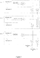
- Figure 1 illustrates a device that can perform automatic fault detection according to one embodiment of the present invention.
- the device includes control logic 141 that sends a signal to a signal tree.
- the control logic 141 sends a test enable signal on test enable line 181 to a signal tree including multiple rows of logic, such as rows of logic in a programmable chip.
- a test enable signal on a test enable line 181 is shown, it should be noted that a variety of signals such as configuration address and data signals can also be sent.
- the rows of logic include rows 101, 103, 105, 107, 111, 113, 115, 117, 121, 123, 125, 127, 131, 133, 135, and 137.
- fault detection circuitry 151 is connected to endpoints of each of the rows of logic to allow fault detection circuitry 151 to monitor signals at the ends of the wires farthest from signal sources, so that any fault that occurs along the length of the wire may be detected, even if there are intervening buffers.
- Fault detection circuitry 151 can be used to monitor a variety of signal trees at the leaves of the signals trees.
- each of the rows of logic may be controlled by fuses 161, 163, 165, 167, 171, 173, 175, and 177 that feed each row.
- these fuses may provide redundancy signals indicating whether redundancy is active for a particular row of logic.
- these redundancy signals may also be monitored by fault detection circuitry.
- Fault detection circuitry 151 may send one or more fault detect signals on fault detect line 183 to control logic 141 upon detecting a fault.
- Figure 2 illustrates one example of fault detection circuitry according to one embodiment of the present invention.
- fault detection circuitry spans three rows 201, 203, and 205.
- Test enable lines 211, 213, and 215 may be connected as inputs to OR gates 221, 223, and 225. If any test enable signal is asserted on lines 211, 213, or 215, the fault detect signal on line 207 is asserted.
- Redundancy lines 231, 233, and 235 are connected as inputs to XOR gates 251, 253, and 255. Also connected to inputs of XOR gates 251, 253, and 255 are fuses 241, 243, and 245.
- Redundancy signals on redundancy lines 231, 233, and 235 are compared to the values maintained in fuses 241, 243, and 245 respectively. If any of the redundancy signals on the redundancy lines 231, 233, and 235 deviate from expected values maintained in fuses 241, 243, and 245, an input to OR gate 261, 263, or 265 is asserted and a fault detect signal on line 209 is asserted.
- Fault detection circuitry can be used to monitor a variety of signals and their associated signal trees and can provide one or more fault detect signals. According to various embodiments, fault detection circuitry outputs only one fault detect signal as any fault in a device should cause the shutdown of the device. In other examples, fault detection circuitry outputs multiple different fault detect signals so that information about the fault can be better determined. In particular embodiments, the time it takes for fault detection circuitry to detect a fault can be reduced by using several layers of sensors, where each sensor in a first layer detects a fault in a subset of the control signals, and the outputs of each sensor in this first layer of sensors is monitored by one or more sensors in a second layer of sensors. The second layer of sensors can output an asserted fault signal if any of the sensors in the first layer of sensors outputs an asserted fault signal. In some examples, numerous layers can be used so that multiple layers of sensors could be used to monitor a single set of control signals.
- fault detection circuitry may also use fault masking.
- Figure 3 illustrates one example of fault detection circuitry using masking.
- a fault detect signal on fault detect line 207 is provided as shown in Figure 2 if a test enable signal is asserted. If the control logic 301 is actually generating a test enable signal and a detected test enable signal is not merely a fault, the fault detect signal on fault detect line 207 will be masked by the AND gate 311. That is, if control logic 301 is asserting a test enable signal on test enable line 303, the signal is inverted at NOT gate 307 and used to mask the fault detect signal on fault detect line 207 at AND gate 311.
- the fault detect signal on fault detect line 209 provided as shown in Figure 2 will be masked by AND gate 313. That is, if control logic 301 asserts a redundancy enable signal on redundancy enable line 305, the redundancy enable signal is inverted at NOT gate 309 and used to mask fault detect signal on fault detect line 209 at AND gate 313.
- the outputs of AND gates 311 and 313 can be provided as inputs to OR gate 315 to send a device fault signal on device fault line 317 if any unmasked fault is detected.
- control logic may mask any of the fault sensors to ignore them.
- Fault sensors can be ignored using fixed values according to one or more programmable values maintained in CRAMS, fuses, etc.
- fault sensors can be ignored by masking using a dynamically varying signal value provided by control logic or user logic.
- the detection of the assertion of one or more clear wires can be ignored when the control logic is initializing a device.
- the detection of one or more address line assertions can be ignored during the time a device is being configured.
- Fault sensors can also be ignored by masking using values output by user logic or values used as input to user logic in a user design.
- control logic may also send a signal directly to fault detection circuitry and identify an output to determine if sensors are operating properly.
- Figure 4 illustrates a technique for implementing fault monitoring.
- mechanisms such as fuses and CRAMs are configured with expected values for signals at 401.
- the signal may be a global or critical signal such as a test enable signal, redundancy enable signal, address and data configuration signal, etc.
- the expected value of an address and data configuration signal should be 0 for all lines during operation mode and should be 0 for all lines except one line during configuration mode.
- signals are monitored at the leaves of a signal tree at 403 lines are asserted simultaneously during configuration.
- a signal may be detected at a fault detection circuitry sensor.
- the fault detection circuitry sensor may be an OR gate connected in a daisy chain of OR gates. The signal may be compared to a reference signal to determine if it deviates from the expected signal value at 407.
- the expected value is a static value provided by a fuse or CRAM. In other examples, the expected value is a static or dynamic value provided by control logic or user logic or even an external source.
- fault detection circuitry may only send a fault signal to control logic 411 if a particular number of perceived faults is detected. Fault handling procedures can then be implemented at 413. Fault handling procedures may include device shutdown, device reset, deletion of cryptographic keys, deletion of data, etc.
- FIG. 5 is a diagrammatic representation showing implementation of a programmable chip.
- An input stage 501 receives selection information typically from a user for logic to be implemented on an electronic device. In one example, the input received is in the form of a high-level language program.
- a generator program 505 creates a logic description and provides the logic description 503 along with other customized logic to any of a variety of synthesis tools, place and route programs, and logic configuration tools to allow a logic description to be implemented on an electronic device.
- an input stage 501 often allows selection and parameterization of components to be used on an electronic device.
- the input stage 501 also allows configuration of hard coded logic.
- components provided to an input stage include prepackaged logic such as intellectual property functions, megafunctions, and intellectual property cores.
- the input stage 501 may be a graphical user interface using wizards for allowing efficient or convenient entry of information.
- the input stage may also be a text interface or a program reading a data file such as a spreadsheet, database table, or schematic to acquire selection information.
- the input stage 501 produces an output containing information about the various modules selected.
- the user may enter security information about individual components that needs to be isolated. For example, different levels of component security and which components are allowed to communicate with each other may be entered.
- the generator program 505 can identify the selections and generate a logic description 503 with information for implementing the various modules.
- the generator program 505 can be a Perl script creating HDL files such as Verilog, Abel, VHDL, and AHDL files from the module information entered by a user.
- the generator program identifies a portion of a high-level language program to accelerate. The other code is left for execution on a processor core.
- the generator program 505 identifies pointers and provides ports for each pointer.
- One tool with generator program capabilities is System on a Programmable Chip (SOPC) Builder available from Altera Corporation of San Jose, CA.
- SOPC System on a Programmable Chip
- the generator program 505 also provides information to a synthesis tool 507 to allow HDL files to be automatically synthesized.
- a logic description is provided directly by a designer. Hookups between various components selected by a user are also interconnected by a generator program.
- Some of the available synthesis tools are Leonardo Spectrum, available from Mentor Graphics Corporation of Wilsonville, Oregon and Synplify available from Synplicity Corporation of Sunnyvale, California.
- the HDL files may contain technology specific code readable only by a synthesis tool.
- the HDL files at this point may also be passed to a simulation tool at a verification stage 509.
- the input stage 501, generator program 505, and synthesis tool 507 can be separate programs.
- the interface between the separate programs can be a database file, a log, or simply messages transmitted between the programs.
- the input stage 501 can send messages directly to the generator program 505 to allow the generator program to create a logic description.
- the generator program can provide information directly to the synthesis tool instead of writing HDL files.
- input stage 501, generator program 505, and synthesis tool 507 can be integrated into a single program.
- a user may select various modules and an integrated program can then take the user selections and output a logic description in the form of a synthesized netlist without intermediate files.
- a logic description is an HDL file such as a VHDL, Abel, AHDL, or Verilog file.
- a logic description may be in various stages of processing between the user selection of components and parameters to the final configuration of the device.
- a logic description is a synthesized netlist such as an Electronic Design Interchange Format Input File (EDF file).
- EDF file is one example of a synthesized netlist file that can be output by the synthesis tool 507.
- a synthesis tool 507 can take HDL files and output EDF files.
- Tools for synthesis allow the implementation of the logic design on an electronic device.
- Some of the available synthesis tools are Leonardo Spectrum, available from Mentor Graphics Corporation of Wilsonville, Oregon and Synplify available from Synplicity Corporation of Sunnyvale, California.
- Synplicity Corporation of Sunnyvale, California.
- Various synthesized netlist formats will be appreciated by one of skill in the art.
- a verification stage 509 typically follows the synthesis stage 507.
- the verification stage checks the accuracy of the design to ensure that an intermediate or final design realizes the expected requirements.
- a verification stage typically includes simulation tools and timing analysis tools. Tools for simulation allow the application of inputs and the observation of outputs without having to implement a physical device. Simulation tools provide designers with cost effective and efficient mechanisms for both functional and timing verification of a design. Functional verification involves the circuit's logical operation independent of timing considerations. Parameters such as gate delays are disregarded.
- Timing verification involves the analysis of the design's operation with timing delays. Setup, hold, and other timing requirements for sequential devices such as flip-flops are confirmed.
- Some available simulation tools include Synopsys VCS, VSS, and Scirocco, available from Synopsys Corporation of Sunnyvale, California and Cadence NC-Verilog and NC-VHDL available from Cadence Design Systems of San Jose, California.
- the synthesized netlist file can be provided to physical design tools 511 including place and route and configuration tools.
- a place and route tool locates logic cells on specific logic elements of a target hardware device and connects wires between the inputs and outputs of the various logic elements in accordance with logic and security provided to implement an electronic design.
- the place and route tool may perform the techniques of the present invention to implement the various security requirements and rules as defined by the user.
- the iterative technique may be transparent to the user, but the resulting device can be physically tested at 513.
- a programmable logic configuration stage can take the output of the place and route tool to program the logic device with the user selected and parameterized modules.
- the place and route tool and the logic configuration stage are provided in the Quartus Development Tool, available from Altera Corporation of San Jose, California.
- a variety of synthesis, place and route, and programmable logic configuration tools can be used using various techniques of the present invention.
- the input stage 501, the generator program 505, the synthesis tool 507, the verification tools 509, and physical design tools 511 are integrated into a single program.
- the various stages are automatically run and transparent to a user.
- the program can receive the user-selected modules, generate a logic description depicting logic for implementing the various selected modules, and implement the electronic device.
- HDL files and EDF files are mere examples of a logic description.
- Other file formats as well as internal program representations are other examples of a logic description.
- FIG. 6 is a diagrammatic representation showing a typical computer system that can be used to implement a device.
- the computer system includes any number of processors 602 (also referred to as central processing units, or CPUs) that are coupled to devices including memory 606 (typically a random access memory, or "RAM"), memory 604 (typically a read only memory, or "ROM").
- the processors 602 can be configured to generate an electronic design.
- memory 604 acts to transfer data and instructions uni-directionally to the CPU and memory 606 are used typically to transfer data and instructions in a bi-directional manner.
- a mass storage device 608 is also coupled bi-directionally to CPU 602 and provides additional data storage capacity and may include any of the computer-readable media described above.
- the mass storage device 608 may be used to store programs, data and the like and is typically a secondary storage medium such as a hard disk that is slower than memory.
- the mass storage device 608 can be used to hold a library or database of prepackaged logic or intellectual property functions, as well as information on generating particular configurations. It will be appreciated that the information retained within the mass storage device 608, may, in appropriate cases, be incorporated in standard fashion as part of memory 606 as virtual memory.
- a specific mass storage device such as an optical drive 614 may also pass data uni-directionally to the CPU.
- CPU 602 is also coupled to an interface 610 that includes one or more input/output devices such as such as video monitors, track balls, mice, keyboards, microphones, touch-sensitive displays, transducer card readers, magnetic or paper tape readers, tablets, styluses, voice or handwriting recognizers, or other well-known input devices such as, of course, other computers.
- the CPU 602 may be a design tool processor.
- CPU 602 optionally may be coupled to a computer or telecommunications network using a network interface as shown generally at 612. With such a network connection, it is contemplated that the CPU might receive information from the network, or might output information to the network in the course of performing the above-described process steps.
- the system 800 might also be associated with devices for transferring completed designs onto a programmable chip. The above-described devices and materials will be familiar to those of skill in the computer hardware and software arts.
Landscapes
- Engineering & Computer Science (AREA)
- Theoretical Computer Science (AREA)
- Physics & Mathematics (AREA)
- General Engineering & Computer Science (AREA)
- General Physics & Mathematics (AREA)
- Quality & Reliability (AREA)
- Semiconductor Integrated Circuits (AREA)
- Tests Of Electronic Circuits (AREA)
- Test And Diagnosis Of Digital Computers (AREA)
Claims (11)
- Integrierte Schaltungseinrichtung, umfassend:Steuerlogik (141, 301), die eingerichtet ist, eine Vielzahl von Signalen (211, 213, 215; 231, 233, 235; 303, 305) auf einen in der integrierten Schaltungseinrichtung enthaltenen Signalbaum mit Zweigen und Blättern zu senden,Nutzerlogik (101, 111), die in der integrierten Schaltungseinrichtung ein Nutzerdesign implementiert, undeine Fehlererkennungsschaltung (151, 201, 203, 205) in der integrierten Schaltungseinrichtung, wobei die Fehlererkennungsschaltung (151, 201, 203, 205) eine Vielzahl von Logikgattern (221, 223, 225; 261, 263, 265) umfasst, die eingerichtet sind, jeweilige Signalwerte einer Vielzahl von Signalwerten an jeweiligen Blättern einer Vielzahl der Blätter an dem Signalbaum zu überwachen, unddadurch gekennzeichnet, dasswobei die Fehlererkennungsschaltung eine erste Verkettung (221, 223, 225) aus ODER-Gattern zum Ausgeben eines ersten Fehlererkennungssignals (207) und eine zweite Verkettung (261, 263, 265) aus ODER-Gattern zum Ausgeben eines zweiten Fehlererkennungssignals (209) umfasst, wobei jeder Zweig des Signalbaums ein erstes ODER-Gatter der ersten Verkettung (221, 223, 225) und ein zweites ODER-Gatter der zweiten ersten Verkettung (261, 263, 265) umfasst, wobei jedes der zwei ODER-Gatter innerhalb jedes Zweigs zum Erkennen eines Fehlers in einem ersten Signalwert (211, 213, 215) und einem zweiten Signalwert (231, 233, 235) der dem jeweiligen Zweig des Signalbaums bereitgestellten Vielzahl von Signalwerten vorgesehen ist,die Fehlererkennungsschaltung (151, 201, 203, 205) eine Maskierungsteilschaltung (311, 313, 315) umfasst, wobei die Maskierungsteilschaltung (311, 313, 315) eingerichtet ist, das erste und/oder zweite Fehlererkennungssignal (207, 209) unter Verwendung jeweiliger UND-Gatter (311, 313) der Maskierungsteilschaltung (311, 313, 315) zu maskieren und die Ausgänge von UND-Gattern (311, 313) unter Verwendung eines ODER-Gatters (315) der Maskierungsteilschaltung (311, 313, 315) zu kombinieren, um ein Einrichtungsfehlersignal (317) an die Steuerlogik (141, 301) auszugeben, unddie Steuerlogik (141, 301) eingerichtet ist, bei Empfangen des einen ersten Wert aufweisenden Einrichtungsfehlersignals (317) von der Maskierungsteilschaltung (311, 313, 315) eine Fehlerbehandlungsprozedur zu implementieren.
- Integrierte Schaltungseinrichtung nach Anspruch 1, wobei die Fehlerbehandlungsprozedur ein Zurücksetzen der Einrichtung und/oder ein Löschen kryptografischer Schlüssel umfasst.
- Integrierte Schaltungseinrichtung nach Anspruch 1 oder 2, wobei es sich bei einem der Vielzahl von Signalen (211, 213, 215; 231, 233, 235; 303, 305) um ein Testfreigabesignal oder ein Adressen- und Datenkonfigurierungssignal handelt.
- Integrierte Schaltungseinrichtung nach einem der Ansprüche 1 bis 3, wobei ein Erwartungswert in einer Sicherung (161-177; 241-245) oder einem Konfigurierungs-Direktzugriffsspeicher aufrechterhalten ist.
- Integrierte Schaltungseinrichtung nach einem der Ansprüche 1 bis 3, wobei es sich bei einem Erwartungswert um eine Variable handelt und diese durch die Steuerlogik (141, 301) oder durch die Nutzerlogik (101, 111) bereitgestellt ist.
- Integrierte Schaltungseinrichtung nach einem von Anspruch 1, wobei die Maskierungsschaltung ferner Folgendes umfasst:einen ersten Inverter (307) zum Empfangen eines Testfreigabesignals (303) und Ausgeben eines invertierten Testfreigabesignals,ein erstes (311) der UND-Gatter (311, 313) mit einem ersten Eingang, der eingerichtet ist, das auf dem ersten Wert befindliche erste Fehlererkennungssignal (207) zu empfangen, und einem zweiten Eingang, der eingerichtet ist, das invertierte Testfreigabesignal zu empfangen,einen zweiten Inverter (2309) zum Empfangen eines Redundanzfreigabesignals (305) und Ausgeben eines invertierten Redundanzfreigabesignals,ein zweites (313) der UND-Gatter (311, 313) mit einem ersten Eingang, der eingerichtet ist, das auf dem ersten Wert befindliche zweite Fehlererkennungssignal (207) zu empfangen, und einem zweiten Eingang, der eingerichtet ist, das invertierte Redundanzfreigabesignal zu empfangen, unddas ODER-Gatter (315), das eingerichtet ist, einen Ausgang aus dem ersten UND-Gatter (311) und einen Ausgang aus dem zweiten UND-Gatter (313) zu empfangen, um das auf dem ersten Wert befindliche Einrichtungsfehlersignal (317) nur dann auszugeben, wenn sowohl das Testfreigabesignal als auch das Redundanzfreigabesignal gesperrt sind.
- Verfahren, das die folgenden Schritte umfasst:Senden, durch eine Steuerlogik (141, 301) in einer integrierten Schaltungseinrichtung, einer Vielzahl von Signalen (211, 213, 215; 231, 233, 235; 303, 305) auf einen in der integrierten Schaltungseinrichtung enthaltenen Signalbaum mit Zweigen und Blättern,Implementieren eines Nutzerdesigns innerhalb einer Nutzerlogik (101, 111) der integrierten Schaltungseinrichtung undÜberwachen jeweiliger Signalwerte einer Vielzahl von Signalwerten an jeweiligen Blättern einer Vielzahl der Blätter an dem Signalbaum unter Verwendung einer in einer Fehlererkennungsschaltung (151, 201, 203, 205) in der integrierten Schaltungseinrichtung umfassten Vielzahl von Logikgattern (221, 223, 225; 261, 263, 265) undgekennzeichnet durchAusgeben eines ersten Fehlererkennungssignals (207) durch eine durch die Fehlererkennungsschaltung (151, 201, 203, 205) umfasste erste Verkettung (221, 223, 225) aus ODER-Gattern,Ausgeben eines zweiten Fehlererkennungssignals (209) und einer durch die Fehlererkennungsschaltung (151, 201, 203, 205) umfassten zweiten Verkettung (261, 263, 265) aus ODER-Gattern,wobei jeder Zweig des Signalbaums ein erstes ODER-Gatter der ersten Verkettung (221, 223, 225) und ein zweites ODER-Gatter der zweiten ersten Verkettung (261, 263, 265) umfasst, wobei jedes der zwei ODER-Gatter innerhalb jedes Zweigs einen Fehler in einem ersten Signalwert (211, 213, 215) und einem zweiten Signalwert (231, 233, 235) der dem jeweiligen Zweig des Signalbaums bereitgestellten Vielzahl von Signalwerten erkennt,Maskieren, durch eine durch die Fehlererkennungsschaltung (151, 201, 203, 205) umfasste Maskierungsteilschaltung (311, 313, 315), des ersten und/oder zweiten Fehlererkennungssignals (207, 209) unter Verwendung jeweiliger UND-Gatter (311, 313) der Maskierungsteilschaltung (311, 313, 315) und zu Kombinieren der Ausgänge von UND-Gattern (311, 313) unter Verwendung eines ODER-Gatters (315) der Maskierungsteilschaltung (311, 313, 315), um ein Einrichtungsfehlersignal (317) an die Steuerlogik (141, 301) auszugeben, undImplementieren, durch die Steuerlogik (141, 301), einer Fehlerbehandlungsprozedur bei Empfangen des einen ersten Wert aufweisenden Einrichtungsfehlersignals (317) von der Maskierungsteilschaltung (311, 313, 315).
- Verfahren nach Anspruch 7, wobei die Fehlerbehandlungsprozedur ein Zurücksetzen der Einrichtung und/oder ein Löschen kryptografischer Schlüssel umfasst.
- Verfahren nach Anspruch 7 oder 8, wobei die Vielzahl von Signalen (211, 213, 215; 231, 233, 235; 303, 305) ein Testfreigabesignal und/oder ein Adressen- und Datenkonfigurierungssignal beinhaltet.
- Verfahren nach einem der Ansprüche 7 bis 9, wobei ein Erwartungswert in einer Sicherung (161-177; 241-245) oder einem Konfigurierungs-Direktzugriffsspeicher aufrechterhalten wird.
- Verfahren nach einem der Ansprüche 7 bis 10, wobei es sich bei einem Erwartungswert um eine durch Steuerlogik (141, 301) oder durch die Nutzerlogik (101, 111) bereitgestellte Variable handelt.
Applications Claiming Priority (1)
| Application Number | Priority Date | Filing Date | Title |
|---|---|---|---|
| US13/405,781 US9235460B2 (en) | 2012-02-27 | 2012-02-27 | Methods and apparatus for automatic fault detection |
Publications (2)
| Publication Number | Publication Date |
|---|---|
| EP2631803A1 EP2631803A1 (de) | 2013-08-28 |
| EP2631803B1 true EP2631803B1 (de) | 2018-05-30 |
Family
ID=47843057
Family Applications (1)
| Application Number | Title | Priority Date | Filing Date |
|---|---|---|---|
| EP13155874.4A Active EP2631803B1 (de) | 2012-02-27 | 2013-02-20 | Verfahren und Vorrichtung zur automatischen Fehlererkennung |
Country Status (3)
| Country | Link |
|---|---|
| US (2) | US9235460B2 (de) |
| EP (1) | EP2631803B1 (de) |
| CN (1) | CN103294048B (de) |
Families Citing this family (11)
| Publication number | Priority date | Publication date | Assignee | Title |
|---|---|---|---|---|
| US9235460B2 (en) | 2012-02-27 | 2016-01-12 | Altera Corporation | Methods and apparatus for automatic fault detection |
| CN104838617B (zh) * | 2012-12-11 | 2018-01-02 | 三菱电机株式会社 | 整合安全装置及整合安全装置中使用的信号处理方法 |
| CN103885442B (zh) * | 2014-04-02 | 2017-01-18 | 莱芜钢铁集团有限公司 | 一种设备闪变故障源捕获系统及方法 |
| CN106706222A (zh) * | 2017-01-09 | 2017-05-24 | 北京中昌天盛科技有限公司 | 检测系统及方法 |
| JP6635602B2 (ja) * | 2017-03-17 | 2020-01-29 | 株式会社東芝 | 故障検出回路 |
| EP3385735B1 (de) * | 2017-04-04 | 2019-12-04 | Secure-IC SAS | Vorrichtung und verfahren zur erkennung von fehlerpunkten |
| EP3514499B1 (de) * | 2018-01-23 | 2020-08-26 | Siemens Aktiengesellschaft | Verifizierung von sensordaten |
| FR3091367B1 (fr) * | 2018-12-28 | 2020-12-18 | St Microelectronics Rousset | Protection d’un microcontrôleur |
| US11181560B2 (en) * | 2019-05-15 | 2021-11-23 | Infineon Technologies Ag | Detecting failure using multiple monitoring modules |
| US12436528B2 (en) * | 2020-07-30 | 2025-10-07 | Tyco Fire & Security Gmbh | Building management system with supervisory fault detection layer |
| US20250217229A1 (en) * | 2023-12-29 | 2025-07-03 | Nxp B.V. | Fault handling for system-on-chip systems |
Family Cites Families (28)
| Publication number | Priority date | Publication date | Assignee | Title |
|---|---|---|---|---|
| US5250909A (en) * | 1992-05-21 | 1993-10-05 | Benz Companies, Inc. | Automatic fault detection system in electrical sensing circuit |
| US5694401A (en) * | 1994-06-27 | 1997-12-02 | Tandem Computers Incorporated | Fault isolation using pseudo-random scan |
| US6115312A (en) | 1997-10-16 | 2000-09-05 | Altera Corporation | Programmable logic device memory cell circuit |
| US6201404B1 (en) | 1998-07-14 | 2001-03-13 | Altera Corporation | Programmable logic device with redundant circuitry |
| US6574761B1 (en) * | 1999-09-27 | 2003-06-03 | Lattice Semiconductor Corp. | On-line testing of the programmable interconnect network in field programmable gate arrays |
| US6864710B1 (en) | 1999-12-30 | 2005-03-08 | Cypress Semiconductor Corp. | Programmable logic device |
| JP4336029B2 (ja) * | 2000-06-19 | 2009-09-30 | 株式会社アドバンテスト | 半導体集積回路の故障シミュレーション方法および故障シミュレータ |
| EP1438662A2 (de) * | 2001-10-11 | 2004-07-21 | Altera Corporation | Fehlererkennung an programmierbaren logischen betriebsmitteln |
| DE10164424A1 (de) | 2001-12-29 | 2003-07-17 | Philips Intellectual Property | Elektrische oder elektronische Schaltungsanordnung sowie zugeordnetes Verfahren |
| US6973600B2 (en) * | 2002-02-01 | 2005-12-06 | Adc Dsl Systems, Inc. | Bit error rate tester |
| US6941498B2 (en) * | 2002-03-07 | 2005-09-06 | Agilent Technologies, Inc. | Technique for debugging an integrated circuit having a parallel scan-chain architecture |
| EP1351065B1 (de) | 2002-04-03 | 2005-06-08 | STMicroelectronics Limited | Feldprogrammierbare Vorrichtung |
| JP4031954B2 (ja) * | 2002-06-11 | 2008-01-09 | 富士通株式会社 | 集積回路の診断装置および診断方法 |
| US7633976B2 (en) * | 2002-09-19 | 2009-12-15 | Industrial Technology Research Institute | Method and apparatus for code group identification and frame synchronization by use of Reed-Solomon decoder and reliability measurement for UMTS W-CDMA |
| US7131043B1 (en) * | 2003-09-25 | 2006-10-31 | Altera Corporation | Automatic testing for programmable networks of control signals |
| US7030647B1 (en) | 2004-03-05 | 2006-04-18 | Altera Corporation | Techniques for configuring programmable logic using on-chip nonvolatile memory |
| US7610526B2 (en) * | 2005-01-24 | 2009-10-27 | Hewlett-Packard Development Company, L.P. | On-chip circuitry for bus validation |
| US7138844B2 (en) | 2005-03-18 | 2006-11-21 | Altera Corporation | Variable delay circuitry |
| US7451373B2 (en) * | 2005-06-17 | 2008-11-11 | Infineon Technologies Ag | Circuit for compression and storage of circuit diagnosis data |
| DE102006005817B4 (de) * | 2006-02-08 | 2014-06-26 | Infineon Technologies Ag | Fehlererkennungsvorrichtung für einen Adressdecoder und Vorrichtung zur Fehlererkennung für einen Adressdecoder |
| US8812885B2 (en) | 2006-12-28 | 2014-08-19 | Texas Instruments Incorporated | Detecting wake-up events for a chip based on an I/O power supply |
| CN102067402A (zh) * | 2008-07-07 | 2011-05-18 | 立维腾制造有限公司 | 一种故障电路断路器 |
| JP2010020839A (ja) * | 2008-07-10 | 2010-01-28 | Panasonic Corp | 半導体記憶装置 |
| CN101413990B (zh) * | 2008-12-03 | 2010-09-08 | 北京大学 | 一种现场可编程门阵列的测试方法及系统 |
| CN101881811B (zh) * | 2009-05-08 | 2012-10-24 | 复旦大学 | 一种可编程逻辑器件互连资源的故障测试方法 |
| US8984367B2 (en) * | 2011-02-25 | 2015-03-17 | Altera Corporation | Error detection and correction circuitry |
| US8378710B1 (en) * | 2011-09-20 | 2013-02-19 | Nxp B.V. | Secure device anti-tampering circuit |
| US9235460B2 (en) | 2012-02-27 | 2016-01-12 | Altera Corporation | Methods and apparatus for automatic fault detection |
-
2012
- 2012-02-27 US US13/405,781 patent/US9235460B2/en active Active
-
2013
- 2013-02-20 EP EP13155874.4A patent/EP2631803B1/de active Active
- 2013-02-26 CN CN201310063900.6A patent/CN103294048B/zh active Active
-
2016
- 2016-01-07 US US14/990,735 patent/US9360522B2/en active Active
Non-Patent Citations (1)
| Title |
|---|
| NISHIGAKI M ET AL: "A FAULT-TOLERANT COMBINATIONAL CIRCUIT WITH FAULT DIAGNOSIS CAPABILITY-TO MASK AND DETECT THE LOSS OF ANY ONE CONNECTION BETWEEN GATE CIRCUITS", SYSTEMS & COMPUTERS IN JAPAN, WILEY, HOBOKEN, NJ, US, vol. 34, no. 11, 1 October 2003 (2003-10-01), pages 67 - 80, XP001178348, ISSN: 0882-1666, DOI: 10.1002/SCJ.10081 * |
Also Published As
| Publication number | Publication date |
|---|---|
| US9235460B2 (en) | 2016-01-12 |
| EP2631803A1 (de) | 2013-08-28 |
| US9360522B2 (en) | 2016-06-07 |
| US20130226498A1 (en) | 2013-08-29 |
| CN103294048B (zh) | 2018-01-02 |
| US20160116536A1 (en) | 2016-04-28 |
| CN103294048A (zh) | 2013-09-11 |
Similar Documents
| Publication | Publication Date | Title |
|---|---|---|
| US9360522B2 (en) | Methods and apparatus for automatic fault detection | |
| US6560743B2 (en) | Cyclic redundancy checking of a field programmable gate array having a SRAM memory architecture | |
| Borecký et al. | Parity driven reconfigurable duplex system | |
| US8065574B1 (en) | Soft error detection logic testing systems and methods | |
| US9041431B1 (en) | Partial reconfiguration and in-system debugging | |
| US6772387B1 (en) | Cyclic redundancy checking of a field programmable gate array having an SRAM memory architecture | |
| Straka et al. | SEU simulation framework for Xilinx FPGA: First step towards testing fault tolerant systems | |
| US9098662B1 (en) | Configuring a device to debug systems in real-time | |
| EP3385735A1 (de) | Vorrichtung und verfahren zur erkennung von fehlerpunkten | |
| US9170911B1 (en) | Protocol error monitoring on an interface between hard logic and soft logic | |
| US9672094B1 (en) | Interconnect circuitry fault detection | |
| US7656189B1 (en) | Trust controller for detecting unauthorized logic in a circuit design | |
| CN114661531A (zh) | 一种针对fpga的细粒度自修复电路和方法 | |
| Lu et al. | C-testable design techniques for iterative logic arrays | |
| US9864830B1 (en) | Method and apparatus for placement and routing of circuit designs | |
| Gericota et al. | On-line self-healing of circuits implemented on reconfigurable FPGAs | |
| Gericota et al. | A self-healing real-time system based on run-time self-reconfiguration | |
| Borecký et al. | Parity Waterfall Method | |
| Straka et al. | Test platform for fault tolerant systems design properties verification | |
| Xu et al. | Design and verification of universal evaluation system for single event effect sensitivity measurement in very-large-scale integrated circuits | |
| Sontakke et al. | Testing nanometer memories: a review of architectures, applications, and challenges. | |
| US20260092965A1 (en) | Scandump simulation and co-simulation for device testing | |
| JP2021534427A (ja) | デジタル回路試験及び分析モジュール、システム及びそれの方法 | |
| Raval et al. | DFT methodology for memory testing on lower technological node | |
| Gericota et al. | A framework for fault tolerant real time systems based on reconfigurable FPGAs |
Legal Events
| Date | Code | Title | Description |
|---|---|---|---|
| PUAI | Public reference made under article 153(3) epc to a published international application that has entered the european phase |
Free format text: ORIGINAL CODE: 0009012 |
|
| AK | Designated contracting states |
Kind code of ref document: A1 Designated state(s): AL AT BE BG CH CY CZ DE DK EE ES FI FR GB GR HR HU IE IS IT LI LT LU LV MC MK MT NL NO PL PT RO RS SE SI SK SM TR |
|
| AX | Request for extension of the european patent |
Extension state: BA ME |
|
| 17P | Request for examination filed |
Effective date: 20140228 |
|
| RBV | Designated contracting states (corrected) |
Designated state(s): AL AT BE BG CH CY CZ DE DK EE ES FI FR GB GR HR HU IE IS IT LI LT LU LV MC MK MT NL NO PL PT RO RS SE SI SK SM TR |
|
| 17Q | First examination report despatched |
Effective date: 20151001 |
|
| GRAP | Despatch of communication of intention to grant a patent |
Free format text: ORIGINAL CODE: EPIDOSNIGR1 |
|
| STAA | Information on the status of an ep patent application or granted ep patent |
Free format text: STATUS: GRANT OF PATENT IS INTENDED |
|
| INTG | Intention to grant announced |
Effective date: 20180213 |
|
| GRAS | Grant fee paid |
Free format text: ORIGINAL CODE: EPIDOSNIGR3 |
|
| GRAA | (expected) grant |
Free format text: ORIGINAL CODE: 0009210 |
|
| STAA | Information on the status of an ep patent application or granted ep patent |
Free format text: STATUS: THE PATENT HAS BEEN GRANTED |
|
| AK | Designated contracting states |
Kind code of ref document: B1 Designated state(s): AL AT BE BG CH CY CZ DE DK EE ES FI FR GB GR HR HU IE IS IT LI LT LU LV MC MK MT NL NO PL PT RO RS SE SI SK SM TR |
|
| REG | Reference to a national code |
Ref country code: GB Ref legal event code: FG4D |
|
| REG | Reference to a national code |
Ref country code: CH Ref legal event code: EP |
|
| REG | Reference to a national code |
Ref country code: AT Ref legal event code: REF Ref document number: 1004311 Country of ref document: AT Kind code of ref document: T Effective date: 20180615 |
|
| REG | Reference to a national code |
Ref country code: IE Ref legal event code: FG4D |
|
| REG | Reference to a national code |
Ref country code: DE Ref legal event code: R096 Ref document number: 602013038007 Country of ref document: DE |
|
| REG | Reference to a national code |
Ref country code: NL Ref legal event code: MP Effective date: 20180530 |
|
| REG | Reference to a national code |
Ref country code: LT Ref legal event code: MG4D |
|
| PG25 | Lapsed in a contracting state [announced via postgrant information from national office to epo] |
Ref country code: ES Free format text: LAPSE BECAUSE OF FAILURE TO SUBMIT A TRANSLATION OF THE DESCRIPTION OR TO PAY THE FEE WITHIN THE PRESCRIBED TIME-LIMIT Effective date: 20180530 Ref country code: NO Free format text: LAPSE BECAUSE OF FAILURE TO SUBMIT A TRANSLATION OF THE DESCRIPTION OR TO PAY THE FEE WITHIN THE PRESCRIBED TIME-LIMIT Effective date: 20180830 Ref country code: CY Free format text: LAPSE BECAUSE OF FAILURE TO SUBMIT A TRANSLATION OF THE DESCRIPTION OR TO PAY THE FEE WITHIN THE PRESCRIBED TIME-LIMIT Effective date: 20180530 Ref country code: SE Free format text: LAPSE BECAUSE OF FAILURE TO SUBMIT A TRANSLATION OF THE DESCRIPTION OR TO PAY THE FEE WITHIN THE PRESCRIBED TIME-LIMIT Effective date: 20180530 Ref country code: LT Free format text: LAPSE BECAUSE OF FAILURE TO SUBMIT A TRANSLATION OF THE DESCRIPTION OR TO PAY THE FEE WITHIN THE PRESCRIBED TIME-LIMIT Effective date: 20180530 Ref country code: FI Free format text: LAPSE BECAUSE OF FAILURE TO SUBMIT A TRANSLATION OF THE DESCRIPTION OR TO PAY THE FEE WITHIN THE PRESCRIBED TIME-LIMIT Effective date: 20180530 Ref country code: BG Free format text: LAPSE BECAUSE OF FAILURE TO SUBMIT A TRANSLATION OF THE DESCRIPTION OR TO PAY THE FEE WITHIN THE PRESCRIBED TIME-LIMIT Effective date: 20180830 |
|
| PG25 | Lapsed in a contracting state [announced via postgrant information from national office to epo] |
Ref country code: RS Free format text: LAPSE BECAUSE OF FAILURE TO SUBMIT A TRANSLATION OF THE DESCRIPTION OR TO PAY THE FEE WITHIN THE PRESCRIBED TIME-LIMIT Effective date: 20180530 Ref country code: LV Free format text: LAPSE BECAUSE OF FAILURE TO SUBMIT A TRANSLATION OF THE DESCRIPTION OR TO PAY THE FEE WITHIN THE PRESCRIBED TIME-LIMIT Effective date: 20180530 Ref country code: GR Free format text: LAPSE BECAUSE OF FAILURE TO SUBMIT A TRANSLATION OF THE DESCRIPTION OR TO PAY THE FEE WITHIN THE PRESCRIBED TIME-LIMIT Effective date: 20180831 Ref country code: HR Free format text: LAPSE BECAUSE OF FAILURE TO SUBMIT A TRANSLATION OF THE DESCRIPTION OR TO PAY THE FEE WITHIN THE PRESCRIBED TIME-LIMIT Effective date: 20180530 |
|
| REG | Reference to a national code |
Ref country code: AT Ref legal event code: MK05 Ref document number: 1004311 Country of ref document: AT Kind code of ref document: T Effective date: 20180530 |
|
| PG25 | Lapsed in a contracting state [announced via postgrant information from national office to epo] |
Ref country code: NL Free format text: LAPSE BECAUSE OF FAILURE TO SUBMIT A TRANSLATION OF THE DESCRIPTION OR TO PAY THE FEE WITHIN THE PRESCRIBED TIME-LIMIT Effective date: 20180530 |
|
| PG25 | Lapsed in a contracting state [announced via postgrant information from national office to epo] |
Ref country code: SK Free format text: LAPSE BECAUSE OF FAILURE TO SUBMIT A TRANSLATION OF THE DESCRIPTION OR TO PAY THE FEE WITHIN THE PRESCRIBED TIME-LIMIT Effective date: 20180530 Ref country code: RO Free format text: LAPSE BECAUSE OF FAILURE TO SUBMIT A TRANSLATION OF THE DESCRIPTION OR TO PAY THE FEE WITHIN THE PRESCRIBED TIME-LIMIT Effective date: 20180530 Ref country code: EE Free format text: LAPSE BECAUSE OF FAILURE TO SUBMIT A TRANSLATION OF THE DESCRIPTION OR TO PAY THE FEE WITHIN THE PRESCRIBED TIME-LIMIT Effective date: 20180530 Ref country code: DK Free format text: LAPSE BECAUSE OF FAILURE TO SUBMIT A TRANSLATION OF THE DESCRIPTION OR TO PAY THE FEE WITHIN THE PRESCRIBED TIME-LIMIT Effective date: 20180530 Ref country code: AT Free format text: LAPSE BECAUSE OF FAILURE TO SUBMIT A TRANSLATION OF THE DESCRIPTION OR TO PAY THE FEE WITHIN THE PRESCRIBED TIME-LIMIT Effective date: 20180530 Ref country code: PL Free format text: LAPSE BECAUSE OF FAILURE TO SUBMIT A TRANSLATION OF THE DESCRIPTION OR TO PAY THE FEE WITHIN THE PRESCRIBED TIME-LIMIT Effective date: 20180530 Ref country code: CZ Free format text: LAPSE BECAUSE OF FAILURE TO SUBMIT A TRANSLATION OF THE DESCRIPTION OR TO PAY THE FEE WITHIN THE PRESCRIBED TIME-LIMIT Effective date: 20180530 |
|
| PG25 | Lapsed in a contracting state [announced via postgrant information from national office to epo] |
Ref country code: IT Free format text: LAPSE BECAUSE OF FAILURE TO SUBMIT A TRANSLATION OF THE DESCRIPTION OR TO PAY THE FEE WITHIN THE PRESCRIBED TIME-LIMIT Effective date: 20180530 Ref country code: SM Free format text: LAPSE BECAUSE OF FAILURE TO SUBMIT A TRANSLATION OF THE DESCRIPTION OR TO PAY THE FEE WITHIN THE PRESCRIBED TIME-LIMIT Effective date: 20180530 |
|
| REG | Reference to a national code |
Ref country code: DE Ref legal event code: R097 Ref document number: 602013038007 Country of ref document: DE |
|
| PLBE | No opposition filed within time limit |
Free format text: ORIGINAL CODE: 0009261 |
|
| STAA | Information on the status of an ep patent application or granted ep patent |
Free format text: STATUS: NO OPPOSITION FILED WITHIN TIME LIMIT |
|
| 26N | No opposition filed |
Effective date: 20190301 |
|
| PG25 | Lapsed in a contracting state [announced via postgrant information from national office to epo] |
Ref country code: SI Free format text: LAPSE BECAUSE OF FAILURE TO SUBMIT A TRANSLATION OF THE DESCRIPTION OR TO PAY THE FEE WITHIN THE PRESCRIBED TIME-LIMIT Effective date: 20180530 |
|
| REG | Reference to a national code |
Ref country code: CH Ref legal event code: PL |
|
| GBPC | Gb: european patent ceased through non-payment of renewal fee |
Effective date: 20190220 |
|
| PG25 | Lapsed in a contracting state [announced via postgrant information from national office to epo] |
Ref country code: LU Free format text: LAPSE BECAUSE OF NON-PAYMENT OF DUE FEES Effective date: 20190220 Ref country code: MC Free format text: LAPSE BECAUSE OF FAILURE TO SUBMIT A TRANSLATION OF THE DESCRIPTION OR TO PAY THE FEE WITHIN THE PRESCRIBED TIME-LIMIT Effective date: 20180530 |
|
| REG | Reference to a national code |
Ref country code: BE Ref legal event code: MM Effective date: 20190228 |
|
| REG | Reference to a national code |
Ref country code: IE Ref legal event code: MM4A |
|
| PG25 | Lapsed in a contracting state [announced via postgrant information from national office to epo] |
Ref country code: AL Free format text: LAPSE BECAUSE OF FAILURE TO SUBMIT A TRANSLATION OF THE DESCRIPTION OR TO PAY THE FEE WITHIN THE PRESCRIBED TIME-LIMIT Effective date: 20180530 |
|
| PG25 | Lapsed in a contracting state [announced via postgrant information from national office to epo] |
Ref country code: CH Free format text: LAPSE BECAUSE OF NON-PAYMENT OF DUE FEES Effective date: 20190228 Ref country code: LI Free format text: LAPSE BECAUSE OF NON-PAYMENT OF DUE FEES Effective date: 20190228 |
|
| PG25 | Lapsed in a contracting state [announced via postgrant information from national office to epo] |
Ref country code: IE Free format text: LAPSE BECAUSE OF NON-PAYMENT OF DUE FEES Effective date: 20190220 Ref country code: GB Free format text: LAPSE BECAUSE OF NON-PAYMENT OF DUE FEES Effective date: 20190220 |
|
| PG25 | Lapsed in a contracting state [announced via postgrant information from national office to epo] |
Ref country code: BE Free format text: LAPSE BECAUSE OF NON-PAYMENT OF DUE FEES Effective date: 20190228 |
|
| PG25 | Lapsed in a contracting state [announced via postgrant information from national office to epo] |
Ref country code: TR Free format text: LAPSE BECAUSE OF FAILURE TO SUBMIT A TRANSLATION OF THE DESCRIPTION OR TO PAY THE FEE WITHIN THE PRESCRIBED TIME-LIMIT Effective date: 20180530 |
|
| PG25 | Lapsed in a contracting state [announced via postgrant information from national office to epo] |
Ref country code: PT Free format text: LAPSE BECAUSE OF FAILURE TO SUBMIT A TRANSLATION OF THE DESCRIPTION OR TO PAY THE FEE WITHIN THE PRESCRIBED TIME-LIMIT Effective date: 20181001 Ref country code: MT Free format text: LAPSE BECAUSE OF NON-PAYMENT OF DUE FEES Effective date: 20190220 |
|
| PG25 | Lapsed in a contracting state [announced via postgrant information from national office to epo] |
Ref country code: IS Free format text: LAPSE BECAUSE OF FAILURE TO SUBMIT A TRANSLATION OF THE DESCRIPTION OR TO PAY THE FEE WITHIN THE PRESCRIBED TIME-LIMIT Effective date: 20180930 |
|
| PG25 | Lapsed in a contracting state [announced via postgrant information from national office to epo] |
Ref country code: HU Free format text: LAPSE BECAUSE OF FAILURE TO SUBMIT A TRANSLATION OF THE DESCRIPTION OR TO PAY THE FEE WITHIN THE PRESCRIBED TIME-LIMIT; INVALID AB INITIO Effective date: 20130220 |
|
| PG25 | Lapsed in a contracting state [announced via postgrant information from national office to epo] |
Ref country code: MK Free format text: LAPSE BECAUSE OF FAILURE TO SUBMIT A TRANSLATION OF THE DESCRIPTION OR TO PAY THE FEE WITHIN THE PRESCRIBED TIME-LIMIT Effective date: 20180530 |
|
| P01 | Opt-out of the competence of the unified patent court (upc) registered |
Effective date: 20230531 |
|
| PGFP | Annual fee paid to national office [announced via postgrant information from national office to epo] |
Ref country code: DE Payment date: 20260217 Year of fee payment: 14 |
|
| PGFP | Annual fee paid to national office [announced via postgrant information from national office to epo] |
Ref country code: FR Payment date: 20260219 Year of fee payment: 14 |