EP2621728B1 - Inkjet printhead having common conductive track on nozzle plate - Google Patents
Inkjet printhead having common conductive track on nozzle plate Download PDFInfo
- Publication number
- EP2621728B1 EP2621728B1 EP10857627.3A EP10857627A EP2621728B1 EP 2621728 B1 EP2621728 B1 EP 2621728B1 EP 10857627 A EP10857627 A EP 10857627A EP 2621728 B1 EP2621728 B1 EP 2621728B1
- Authority
- EP
- European Patent Office
- Prior art keywords
- conductive track
- inkjet printhead
- nozzle
- printhead
- actuator
- Prior art date
- Legal status (The legal status is an assumption and is not a legal conclusion. Google has not performed a legal analysis and makes no representation as to the accuracy of the status listed.)
- Not-in-force
Links
Images

Classifications
-
- B—PERFORMING OPERATIONS; TRANSPORTING
- B41—PRINTING; LINING MACHINES; TYPEWRITERS; STAMPS
- B41J—TYPEWRITERS; SELECTIVE PRINTING MECHANISMS, i.e. MECHANISMS PRINTING OTHERWISE THAN FROM A FORME; CORRECTION OF TYPOGRAPHICAL ERRORS
- B41J2/00—Typewriters or selective printing mechanisms characterised by the printing or marking process for which they are designed
- B41J2/005—Typewriters or selective printing mechanisms characterised by the printing or marking process for which they are designed characterised by bringing liquid or particles selectively into contact with a printing material
- B41J2/01—Ink jet
- B41J2/135—Nozzles
- B41J2/145—Arrangement thereof
- B41J2/155—Arrangement thereof for line printing
-
- B—PERFORMING OPERATIONS; TRANSPORTING
- B41—PRINTING; LINING MACHINES; TYPEWRITERS; STAMPS
- B41J—TYPEWRITERS; SELECTIVE PRINTING MECHANISMS, i.e. MECHANISMS PRINTING OTHERWISE THAN FROM A FORME; CORRECTION OF TYPOGRAPHICAL ERRORS
- B41J2/00—Typewriters or selective printing mechanisms characterised by the printing or marking process for which they are designed
- B41J2/005—Typewriters or selective printing mechanisms characterised by the printing or marking process for which they are designed characterised by bringing liquid or particles selectively into contact with a printing material
- B41J2/01—Ink jet
- B41J2/015—Ink jet characterised by the jet generation process
- B41J2/04—Ink jet characterised by the jet generation process generating single droplets or particles on demand
- B41J2/045—Ink jet characterised by the jet generation process generating single droplets or particles on demand by pressure, e.g. electromechanical transducers
- B41J2/04501—Control methods or devices therefor, e.g. driver circuits, control circuits
- B41J2/04585—Control methods or devices therefor, e.g. driver circuits, control circuits controlling heads based on thermal bent actuators
-
- B—PERFORMING OPERATIONS; TRANSPORTING
- B41—PRINTING; LINING MACHINES; TYPEWRITERS; STAMPS
- B41J—TYPEWRITERS; SELECTIVE PRINTING MECHANISMS, i.e. MECHANISMS PRINTING OTHERWISE THAN FROM A FORME; CORRECTION OF TYPOGRAPHICAL ERRORS
- B41J2/00—Typewriters or selective printing mechanisms characterised by the printing or marking process for which they are designed
- B41J2/005—Typewriters or selective printing mechanisms characterised by the printing or marking process for which they are designed characterised by bringing liquid or particles selectively into contact with a printing material
- B41J2/01—Ink jet
- B41J2/015—Ink jet characterised by the jet generation process
- B41J2/04—Ink jet characterised by the jet generation process generating single droplets or particles on demand
- B41J2/045—Ink jet characterised by the jet generation process generating single droplets or particles on demand by pressure, e.g. electromechanical transducers
- B41J2/04501—Control methods or devices therefor, e.g. driver circuits, control circuits
- B41J2/04591—Width of the driving signal being adjusted
-
- B—PERFORMING OPERATIONS; TRANSPORTING
- B41—PRINTING; LINING MACHINES; TYPEWRITERS; STAMPS
- B41J—TYPEWRITERS; SELECTIVE PRINTING MECHANISMS, i.e. MECHANISMS PRINTING OTHERWISE THAN FROM A FORME; CORRECTION OF TYPOGRAPHICAL ERRORS
- B41J2/00—Typewriters or selective printing mechanisms characterised by the printing or marking process for which they are designed
- B41J2/005—Typewriters or selective printing mechanisms characterised by the printing or marking process for which they are designed characterised by bringing liquid or particles selectively into contact with a printing material
- B41J2/01—Ink jet
- B41J2/135—Nozzles
- B41J2/16—Production of nozzles
- B41J2/1621—Manufacturing processes
- B41J2/1626—Manufacturing processes etching
- B41J2/1628—Manufacturing processes etching dry etching
-
- B—PERFORMING OPERATIONS; TRANSPORTING
- B41—PRINTING; LINING MACHINES; TYPEWRITERS; STAMPS
- B41J—TYPEWRITERS; SELECTIVE PRINTING MECHANISMS, i.e. MECHANISMS PRINTING OTHERWISE THAN FROM A FORME; CORRECTION OF TYPOGRAPHICAL ERRORS
- B41J2/00—Typewriters or selective printing mechanisms characterised by the printing or marking process for which they are designed
- B41J2/005—Typewriters or selective printing mechanisms characterised by the printing or marking process for which they are designed characterised by bringing liquid or particles selectively into contact with a printing material
- B41J2/01—Ink jet
- B41J2/135—Nozzles
- B41J2/16—Production of nozzles
- B41J2/1621—Manufacturing processes
- B41J2/1637—Manufacturing processes molding
- B41J2/1639—Manufacturing processes molding sacrificial molding
-
- B—PERFORMING OPERATIONS; TRANSPORTING
- B41—PRINTING; LINING MACHINES; TYPEWRITERS; STAMPS
- B41J—TYPEWRITERS; SELECTIVE PRINTING MECHANISMS, i.e. MECHANISMS PRINTING OTHERWISE THAN FROM A FORME; CORRECTION OF TYPOGRAPHICAL ERRORS
- B41J2/00—Typewriters or selective printing mechanisms characterised by the printing or marking process for which they are designed
- B41J2/005—Typewriters or selective printing mechanisms characterised by the printing or marking process for which they are designed characterised by bringing liquid or particles selectively into contact with a printing material
- B41J2/01—Ink jet
- B41J2/135—Nozzles
- B41J2/16—Production of nozzles
- B41J2/1621—Manufacturing processes
- B41J2/164—Manufacturing processes thin film formation
- B41J2/1643—Manufacturing processes thin film formation thin film formation by plating
-
- B—PERFORMING OPERATIONS; TRANSPORTING
- B41—PRINTING; LINING MACHINES; TYPEWRITERS; STAMPS
- B41J—TYPEWRITERS; SELECTIVE PRINTING MECHANISMS, i.e. MECHANISMS PRINTING OTHERWISE THAN FROM A FORME; CORRECTION OF TYPOGRAPHICAL ERRORS
- B41J2/00—Typewriters or selective printing mechanisms characterised by the printing or marking process for which they are designed
- B41J2/005—Typewriters or selective printing mechanisms characterised by the printing or marking process for which they are designed characterised by bringing liquid or particles selectively into contact with a printing material
- B41J2/01—Ink jet
- B41J2/135—Nozzles
- B41J2/16—Production of nozzles
- B41J2/1648—Production of print heads with thermal bend detached actuators
-
- B—PERFORMING OPERATIONS; TRANSPORTING
- B41—PRINTING; LINING MACHINES; TYPEWRITERS; STAMPS
- B41J—TYPEWRITERS; SELECTIVE PRINTING MECHANISMS, i.e. MECHANISMS PRINTING OTHERWISE THAN FROM A FORME; CORRECTION OF TYPOGRAPHICAL ERRORS
- B41J2/00—Typewriters or selective printing mechanisms characterised by the printing or marking process for which they are designed
- B41J2/005—Typewriters or selective printing mechanisms characterised by the printing or marking process for which they are designed characterised by bringing liquid or particles selectively into contact with a printing material
- B41J2/01—Ink jet
- B41J2/21—Ink jet for multi-colour printing
- B41J2/2132—Print quality control characterised by dot disposition, e.g. for reducing white stripes or banding
- B41J2/2146—Print quality control characterised by dot disposition, e.g. for reducing white stripes or banding for line print heads
-
- B—PERFORMING OPERATIONS; TRANSPORTING
- B41—PRINTING; LINING MACHINES; TYPEWRITERS; STAMPS
- B41J—TYPEWRITERS; SELECTIVE PRINTING MECHANISMS, i.e. MECHANISMS PRINTING OTHERWISE THAN FROM A FORME; CORRECTION OF TYPOGRAPHICAL ERRORS
- B41J2/00—Typewriters or selective printing mechanisms characterised by the printing or marking process for which they are designed
- B41J2/005—Typewriters or selective printing mechanisms characterised by the printing or marking process for which they are designed characterised by bringing liquid or particles selectively into contact with a printing material
- B41J2/01—Ink jet
- B41J2/135—Nozzles
- B41J2/14—Structure thereof only for on-demand ink jet heads
- B41J2/14427—Structure of ink jet print heads with thermal bend detached actuators
- B41J2002/14435—Moving nozzle made of thermal bend detached actuator
-
- B—PERFORMING OPERATIONS; TRANSPORTING
- B41—PRINTING; LINING MACHINES; TYPEWRITERS; STAMPS
- B41J—TYPEWRITERS; SELECTIVE PRINTING MECHANISMS, i.e. MECHANISMS PRINTING OTHERWISE THAN FROM A FORME; CORRECTION OF TYPOGRAPHICAL ERRORS
- B41J2/00—Typewriters or selective printing mechanisms characterised by the printing or marking process for which they are designed
- B41J2/005—Typewriters or selective printing mechanisms characterised by the printing or marking process for which they are designed characterised by bringing liquid or particles selectively into contact with a printing material
- B41J2/01—Ink jet
- B41J2/135—Nozzles
- B41J2/14—Structure thereof only for on-demand ink jet heads
- B41J2002/14491—Electrical connection
-
- B—PERFORMING OPERATIONS; TRANSPORTING
- B41—PRINTING; LINING MACHINES; TYPEWRITERS; STAMPS
- B41J—TYPEWRITERS; SELECTIVE PRINTING MECHANISMS, i.e. MECHANISMS PRINTING OTHERWISE THAN FROM A FORME; CORRECTION OF TYPOGRAPHICAL ERRORS
- B41J2202/00—Embodiments of or processes related to ink-jet or thermal heads
- B41J2202/01—Embodiments of or processes related to ink-jet heads
- B41J2202/18—Electrical connection established using vias
Definitions
- the present invention relates to the field of printers and particularly inkjet printheads. It has been developed primarily to improve print quality and printhead performance in high resolution printheads.
- Ink Jet printers themselves come in many different types.
- the utilization of a continuous stream of ink in ink jet printing appears to date back to at least 1929 wherein US Patent No. 1941001 by Hansell discloses a simple form of continuous stream electro-static ink jet printing.
- US Patent 3596275 by Sweet also discloses a process of a continuous ink jet printing including the step wherein the ink jet stream is modulated by a high frequency electro-static field so as to cause drop separation. This technique is still utilized by several manufacturers including Elmjet and Scitex (see also US Patent No. 3373437 by Sweet et al )
- Piezoelectric ink jet printers are also one form of commonly utilized ink jet printing device. Piezoelectric systems are disclosed by Kyser et. al. in US Patent No. 3946398 (1970 ) which utilizes a diaphragm mode of operation, by Zolten in US Patent 3683212 (1970 ) which discloses a squeeze mode of operation of a piezoelectric crystal, Stemme in US Patent No. 3747120 (1972 ) discloses a bend mode of piezoelectric operation, Howkins in US Patent No. 4459601 discloses a piezoelectric push mode actuation of the ink jet stream and Fischbeck in US 4584590 which discloses a shear mode type of piezoelectric transducer element.
- the ink jet printing techniques include those disclosed by Endo et al in GB 2007162 (1979 ) and Vaught et al in US Patent 4490728 . Both the aforementioned references disclosed ink jet printing techniques that rely upon the activation of an electrothermal actuator which results in the creation of a bubble in a constricted space, such as a nozzle, which thereby causes the ejection of ink from an aperture connected to the confined space onto a relevant print media.
- Printing devices utilizing the electrothermal actuator are manufactured by manufacturers such as Canon and Hewlett Packard.
- a printing technology should have a number of desirable attributes. These include inexpensive construction and operation, high speed operation, safe and continuous long term operation etc. Each technology may have its own advantages and disadvantages in the areas of cost, speed, quality, reliability, power usage, simplicity of construction operation, durability and consumables.
- the present Applicant has disclosed a plethora of pagewidth printhead designs. Stationary page with printheads, which extend across a width of a page, present a number of unique design challenges when compared with more conventional traversing inkjet printheads.
- pagewidth printheads are typically built up from a plurality of individual printhead integrated circuits (ICs), which must be joined seamlessly to provide high print quality.
- ICs integrated circuits
- the present Applicant has hitherto described printheads having a displaced section of nozzles, which enables nozzle rows to print seamlessly between abutting printhead integrated circuits spanning across a pagewidth (see US Patent Nos. 7,390,071 and 7,290,852 ).
- Other approaches to pagewidth printing e.g .
- HP EdgelineTM Technology employ staggered printhead modules, which inevitably increase the size of the print zone and place additional demands on media feed mechanisms in order to maintain proper alignment with the print zone. It would be desirable to provide an alternative nozzle design, which enables a new approach to the construction of pagewidth printheads.
- pagewidth printheads typically include 'redundant' nozzle rows, which may be used for dead nozzle compensation or for modulating a peak power requirement of the printhead (see US Patent Nos. 7,465,017 and 7,252,353 ).
- Dead nozzle compensation is a particular problem in stationary pagewidth printheads, in contrast with traversing printheads, because the media substrate only makes a single pass of each nozzle in the printhead during printing. Redundancy inevitably increases the cost and complexity of pagewidth printheads, and it would be desirable to minimize redundant nozzle row(s) whilst still providing adequate mechanisms for dead nozzle compensation.
- the document US 2004/104973 A1 discloses a fluid injection head structure which is formed on a substrate and has a manifold therein, bubble generators, a conductive trace, and at least two rows of chambers adjacent to the manifold in flow communication with the manifold.
- the conductive trace disposed on a top surface of the substrate and partially disposed between the two rows of the chambers above the manifold is used to drive the bubble generator.
- MEMS printhead design An important aspect of MEMS printhead design is the integration of MEMS actuators with underlying CMOS drive circuitry.
- current from a drive transistor in the CMOS drive circuitry layer must flow up into the MEMS layer, through the actuator and back down to the CMOS drive circuitry layer (e.g. to a ground plane in the CMOS layer).
- the efficiency of current flow paths should be maximized so as to minimize losses in overall printhead efficiency.
- nozzle assemblies having a pair of linear posts extending between a MEMS actuator (positioned in the nozzle chamber roof) and an underlying CMOS drive circuitry layer.
- Linear copper posts extending up to the MEMS layer as opposed to more tortuous current pathways, have been shown to improve printhead efficiency. Nevertheless, there is still scope for improving the electrical efficiency of the Applicant's MEMS printheads (and printhead ICs).
- Ground bounce is a well known problem in integrated circuit design, which is particularly exacerbated by having a large number of devices powered between common power and ground planes. Ground bounce usually describes an unwanted voltage drop across either a power or ground plane, which may arise from many different sources. Typical sources of ground bounce include: series resistance ("IR drop”), self-inductance, and mutual inductance between ground and power planes. Each of these phenomena may contribute to ground bounce by undesirably decreasing the potential difference between power and ground planes. This decreased potential difference inevitably results in reduced electrical efficiency of the integrated circuit, more particularly the printhead IC in the present case. It will be appreciated that the arrangement and configuration of power and ground planes, as well as connections thereto, can fundamentally affect ground bounce and the overall efficiency of a printhead.
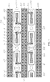
- FIG. 1 there is shown in plan view part of a printhead IC 300 having conductive tracks extending longitudinally and parallel with nozzle rows.
- the uppermost polymer layer 19 has been removed for clarity in Figure 1 .
- a plurality of nozzles 210 are arranged in nozzle rows extending along a longitudinal axis of the printhead IC 300.
- Figure 1 shows a pair of nozzle rows 302A and 302B, although the printhead IC 300 may of course comprises more nozzle rows.
- the nozzle rows 302A and 302B are paired and offset from each other, with one nozzle row 302A being responsible for printing 'even' dots and the other nozzle row 302B being responsible for printing 'odd' dots.
- a first conductive track 303 is positioned between the nozzle rows 302A and 302B.
- the first conductive track 303 is deposited on the nozzle plate 304 of the printhead IC 300, which defines the nozzle chamber roofs 7.
- the first conductive track 303 is generally coplanar with the thermoelastic beams 10 of the actuators 15 and may be formed during MEMS fabrication by co-deposition with the thermoelastic beam material (e.g . vanadium-aluminium alloy).
- Conductivity of the conductive track 303 may be further improved by deposition of another conductive metal layer (e.g. copper, titanium, aluminium etc ) during MEMS fabrication.
- another conductive metal layer e.g. copper, titanium, aluminium etc
- the conductive track 303 may comprise multiple metal layers so as to optimize conductivity.
- Each actuator 15 has a first terminal directly connected to the first conductive track 303 via a transverse connector 305.
- each actuator from both nozzle rows 302A and 302B has a first terminal connected to the first conductive track 303.
- the first conductive track 303 is connected to a common reference plane in the underlying CMOS drive circuitry layer via a plurality of conductor posts 307.
- the conductive track 303 may extend continuously along the printhead IC 300 to provide a common reference plane for each actuator in the pair of nozzle rows.
- the common reference plane between the nozzle rows 302A and 302B may be a power plane or a ground plane, depending on whether nFETs or pFETs are employed in the CMOS drive circuitry.
- the conductive track 303 may extend discontinuously along the printhead IC 300, with each portion of the conductive track providing a common reference plane for a set of actuators.
- a discontinuous conductive track 303 may be preferable in cases where delamination of the conductive track is problematic, although the conductive track still functions in the same manner as described above.
- each actuator 15 is connected to an underlying drive FET in the CMOS drive circuitry layer via an actuator post 8 extending between the actuator and the CMOS drive circuitry layer.
- each actuator 15 is individually controlled by a respective drive FET.
- a pair of second conductive tracks 310A and 310B also extend longitudinally along the printhead IC 300 and flank the pair of nozzle rows 302A and 302B.
- the second conductive tracks 310A and 310B complement the first conductive track 303. In other words, if the first conductive track 303 is a power plane, then the second conductive tracks are both ground planes. Conversely, if the first conductive track 303 is a ground plane, then the second conductive tracks are both power planes.
- the second conductive tracks 310A and 310B are not directly connected to the actuators 15; however, they are connected to a corresponding reference plane (power or ground) in the CMOS drive circuitry layer via a plurality of conductor posts 307.
- the second conductive tracks 310 may be formed during MEMS fabrication in an entirely analogous manner to the first conductive track 303, as described above. Accordingly, the second conductive tracks 310 are typically comprised of the thermoelastic beam material and may be multiple-layered so as to enhance conductivity.
- the first and second conductive tracks 303 and 310 function primarily to reduce the series resistance of corresponding reference planes in the CMOS drive circuitry layer.
- the conductive tracks are configured so as to minimize their resistance, for example by maximizing their width or depth as far as possible.
- the series resistance of a ground plane or a power plane may be reduced by at least 25%, at least 50%, at least 75% or at least 90% by virtue of the conductive tracks in the MEMS layer.
- the self-inductance of a ground plane or a power plane may be similarly reduced. This significant reduction in series resistance and self-inductance of both ground and power planes helps to minimize ground bounce in the printhead IC 300 and therefore improves printhead efficiency. It is understood by the present inventors that mutual inductance between power and ground planes is also be reduced in the printhead IC 300 shown in Figure 1 , although quantitative analysis of mutual inductance requires complex modeling, which is beyond the scope of this disclosure.
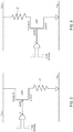
- Figures 2 and 3 provide simplified CMOS circuit diagrams for a pFET and a nFET drive transistor.
- the drive transistor (either nFET or pFET) is directly connected to the second terminal of each actuator 15 via the actuator post 8, as shown in Figure 1 .
- the actuator 15 is connected between the drain of a pFET and the ground plane ("Vss").
- the power plane (“Vpos") is connected to the source of the pFET, while the gate receives the logic fire signal.
- the pFET receives a low voltage at the gate (by virtue of the NAND gate)
- current flows through the pFET so that the actuator 15 is actuated.
- the first terminal of the actuator is connected to the ground plane provided by the first conductive track 303, while the second terminal of the actuator is connected to the pFET.
- the second conductive tracks provide power planes.
- the actuator 15 is connected between the power plane ("Vpos”) and the source of a nFET.
- the ground plane (“Vss”) is connected to the drain of the nFET, while the gate receives the logic fire signal.
- the nFET receives a high voltage at the gate (by virtue of the AND gate)
- current flows through the nFET so that the actuator 15 is actuated.
- the first terminal of the actuator is connected to the power plane provided by the first conductive track 303, while the second terminal of the actuator is connected to the nFET.
- the second conductive tracks provide ground planes.
- first and second conductive tracks 303 and 310 are compatible with either pFETs or nFETs.
- Figure 4 shows a printhead IC 400 comprising a plurality of nozzles 100 arranged in a longitudinally extending pair of nozzle rows 302A and 302B.
- the first conductive track 303 extends between the pair of nozzle rows 302A and 302B, and the second conductive tracks 310A and 310B flank the pair of nozzle rows.
- Each actuator 15 of a respective nozzle 100 has a first terminal connected to the first conductive track 303 via a transverse connector 305, and a second terminal is connected to an underlying FET via an actuator post 8.
- the printhead IC 400 functions analogously to the printhead IC 300 in the sense that the conductive tracks 303 and 310 provide common reference planes by virtue of connections to corresponding reference planes in underlying CMOS drive circuitry. Moreover, the first conductive track 303 is directly connected to one terminal of each actuator so as to provide a common reference plane for each actuator in both nozzle rows 302A and 302B.
Landscapes
- Engineering & Computer Science (AREA)
- Manufacturing & Machinery (AREA)
- Quality & Reliability (AREA)
- Particle Formation And Scattering Control In Inkjet Printers (AREA)
Applications Claiming Priority (1)
| Application Number | Priority Date | Filing Date | Title |
|---|---|---|---|
| PCT/AU2010/001292 WO2012040765A1 (en) | 2010-10-01 | 2010-10-01 | Inkjet printhead having common conductive track on nozzle plate |
Publications (3)
| Publication Number | Publication Date |
|---|---|
| EP2621728A1 EP2621728A1 (en) | 2013-08-07 |
| EP2621728A4 EP2621728A4 (en) | 2015-05-27 |
| EP2621728B1 true EP2621728B1 (en) | 2019-02-13 |
Family
ID=45891710
Family Applications (1)
| Application Number | Title | Priority Date | Filing Date |
|---|---|---|---|
| EP10857627.3A Not-in-force EP2621728B1 (en) | 2010-10-01 | 2010-10-01 | Inkjet printhead having common conductive track on nozzle plate |
Country Status (7)
| Country | Link |
|---|---|
| EP (1) | EP2621728B1 (enExample) |
| JP (1) | JP5692881B2 (enExample) |
| KR (1) | KR101723262B1 (enExample) |
| CN (1) | CN103370201B (enExample) |
| AU (1) | AU2010361609B2 (enExample) |
| SG (1) | SG189013A1 (enExample) |
| WO (1) | WO2012040765A1 (enExample) |
Families Citing this family (4)
| Publication number | Priority date | Publication date | Assignee | Title |
|---|---|---|---|---|
| GB2539052B (en) * | 2015-06-05 | 2020-01-01 | Xaar Technology Ltd | Inkjet printhead |
| EP3969285B1 (en) | 2019-07-17 | 2024-04-24 | Scrona AG | Electrohydrodynamic print head with structured feed layer |
| EP4210955B1 (en) * | 2020-09-09 | 2024-10-02 | Memjet Technology Limited | Method and print chip for single-pass monochrome printing at high speeds |
| WO2022161716A1 (en) * | 2021-01-29 | 2022-08-04 | Memjet Technology Limited | Thermal bend actuator having improved lifetime |
Family Cites Families (13)
| Publication number | Priority date | Publication date | Assignee | Title |
|---|---|---|---|---|
| WO1996032267A1 (en) * | 1995-04-12 | 1996-10-17 | Eastman Kodak Company | Constructions and manufacturing processes for thermally activated print heads |
| US6648453B2 (en) * | 1997-07-15 | 2003-11-18 | Silverbrook Research Pty Ltd | Ink jet printhead chip with predetermined micro-electromechanical systems height |
| US6623108B2 (en) * | 1998-10-16 | 2003-09-23 | Silverbrook Research Pty Ltd | Ink jet printhead having thermal bend actuator heating element electrically isolated from nozzle chamber ink |
| US6265301B1 (en) * | 1999-05-12 | 2001-07-24 | Taiwan Semiconductor Manufacturing Company | Method of forming metal interconnect structures and metal via structures using photolithographic and electroplating or electro-less plating procedures |
| US6938993B2 (en) | 2002-10-31 | 2005-09-06 | Benq Corporation | Fluid injection head structure |
| JP3972363B2 (ja) * | 2003-06-11 | 2007-09-05 | ソニー株式会社 | 液体吐出装置及び液体吐出方法 |
| JP4537159B2 (ja) * | 2003-09-08 | 2010-09-01 | キヤノン株式会社 | 液体吐出ヘッド用半導体装置、液体吐出へッド及び液体吐出装置 |
| US7252353B2 (en) | 2004-05-27 | 2007-08-07 | Silverbrook Research Pty Ltd | Printer controller for supplying data to a printhead module having one or more redundant nozzle rows |
| TWI253395B (en) * | 2005-01-13 | 2006-04-21 | Benq Corp | Fluid injector |
| US7465017B2 (en) | 2005-12-05 | 2008-12-16 | Silverbrook Research Pty Ltd | Dot-at-a-time redundancy for modulating printhead peak power requirement |
| JP2008044310A (ja) * | 2006-08-21 | 2008-02-28 | Canon Inc | インクジェット記録ヘッド |
| US7866795B2 (en) * | 2007-06-15 | 2011-01-11 | Silverbrook Research Pty Ltd | Method of forming connection between electrode and actuator in an inkjet nozzle assembly |
| US8226213B2 (en) * | 2008-05-05 | 2012-07-24 | Zamtec Limited | Short pulsewidth actuation of thermal bend actuator |
-
2010
- 2010-10-01 AU AU2010361609A patent/AU2010361609B2/en not_active Ceased
- 2010-10-01 SG SG2013019849A patent/SG189013A1/en unknown
- 2010-10-01 KR KR1020137010958A patent/KR101723262B1/ko not_active Expired - Fee Related
- 2010-10-01 WO PCT/AU2010/001292 patent/WO2012040765A1/en not_active Ceased
- 2010-10-01 CN CN201080070167.5A patent/CN103370201B/zh not_active Expired - Fee Related
- 2010-10-01 EP EP10857627.3A patent/EP2621728B1/en not_active Not-in-force
- 2010-10-01 JP JP2013530490A patent/JP5692881B2/ja not_active Expired - Fee Related
Non-Patent Citations (1)
| Title |
|---|
| None * |
Also Published As
| Publication number | Publication date |
|---|---|
| KR101723262B1 (ko) | 2017-04-04 |
| SG189013A1 (en) | 2013-05-31 |
| JP2013538711A (ja) | 2013-10-17 |
| CN103370201A (zh) | 2013-10-23 |
| JP5692881B2 (ja) | 2015-04-01 |
| WO2012040765A1 (en) | 2012-04-05 |
| EP2621728A4 (en) | 2015-05-27 |
| EP2621728A1 (en) | 2013-08-07 |
| AU2010361609A1 (en) | 2013-03-21 |
| AU2010361609B2 (en) | 2014-08-14 |
| KR20130141499A (ko) | 2013-12-26 |
| CN103370201B (zh) | 2015-07-15 |
Similar Documents
| Publication | Publication Date | Title |
|---|---|---|
| JP5038460B2 (ja) | 液体吐出ヘッド | |
| US20120019597A1 (en) | Inkjet printhead with cross-slot conductor routing | |
| EP2621728B1 (en) | Inkjet printhead having common conductive track on nozzle plate | |
| US8434844B2 (en) | Stationary inkjet printhead with dead nozzle compensation provided by nozzles in same nozzles row | |
| US8485623B2 (en) | Pagewidth inkjet printhead configured such that printed dot density exceeds nozzle density | |
| US8714677B2 (en) | Inkjet printhead with join regions seamlessly compensated by directional nozzles | |
| US8388111B2 (en) | Method of printing at dot density exceeding nozzle density in stationary pagewidth printhead | |
| US8353577B2 (en) | Method of controlling drop directionality from inkjet nozzle using multiple independently-actuable roof paddles | |
| US8506052B2 (en) | Inkjet nozzle assembly with drop directionality control via independently actuable roof paddles | |
| US8002386B2 (en) | Inkjet printhead having nozzle chambers with redundant ink inlets | |
| CN105058985B (zh) | 通过可独立致动的腔顶桨状物控制墨滴方向性的喷墨喷嘴组件 | |
| US8485638B2 (en) | Inkjet printhead having common conductive track on nozzle plate | |
| US8356884B2 (en) | Printhead integrated circuit having common conductive track fused to nozzle plate | |
| US8342643B2 (en) | Printhead integrated circuit with end nozzles firing at multiple dot positions | |
| AU2014262188B2 (en) | Inkjet nozzle assembly with drop directionality control via independently actuable roof paddles | |
| US8540344B2 (en) | Pagewidth inkjet printhead with drop directionality control | |
| US8348388B2 (en) | Printhead integrated circuit with printable zone longer than nozzle row | |
| US8529005B2 (en) | Method of compensating for dead nozzles in stationary pagewidth printhead | |
| WO2012040766A1 (en) | Inkjet nozzle assembly with drop directionality control via independently actuable roof paddles | |
| TW201215513A (en) | Inkjet printhead having common conductive track on nozzle plate |
Legal Events
| Date | Code | Title | Description |
|---|---|---|---|
| PUAI | Public reference made under article 153(3) epc to a published international application that has entered the european phase |
Free format text: ORIGINAL CODE: 0009012 |
|
| 17P | Request for examination filed |
Effective date: 20130410 |
|
| AK | Designated contracting states |
Kind code of ref document: A1 Designated state(s): AL AT BE BG CH CY CZ DE DK EE ES FI FR GB GR HR HU IE IS IT LI LT LU LV MC MK MT NL NO PL PT RO RS SE SI SK SM TR |
|
| DAX | Request for extension of the european patent (deleted) | ||
| RAP1 | Party data changed (applicant data changed or rights of an application transferred) |
Owner name: ZAMTEC LIMITED |
|
| RAP1 | Party data changed (applicant data changed or rights of an application transferred) |
Owner name: MEMJET TECHNOLOLGY LIMITED |
|
| RAP1 | Party data changed (applicant data changed or rights of an application transferred) |
Owner name: MEMJET TECHNOLOGY LIMITED |
|
| RA4 | Supplementary search report drawn up and despatched (corrected) |
Effective date: 20150428 |
|
| RIC1 | Information provided on ipc code assigned before grant |
Ipc: B41J 29/00 20060101ALI20150421BHEP Ipc: B41J 2/145 20060101AFI20150421BHEP |
|
| STAA | Information on the status of an ep patent application or granted ep patent |
Free format text: STATUS: EXAMINATION IS IN PROGRESS |
|
| 17Q | First examination report despatched |
Effective date: 20170223 |
|
| GRAP | Despatch of communication of intention to grant a patent |
Free format text: ORIGINAL CODE: EPIDOSNIGR1 |
|
| STAA | Information on the status of an ep patent application or granted ep patent |
Free format text: STATUS: GRANT OF PATENT IS INTENDED |
|
| INTG | Intention to grant announced |
Effective date: 20181018 |
|
| GRAS | Grant fee paid |
Free format text: ORIGINAL CODE: EPIDOSNIGR3 |
|
| GRAA | (expected) grant |
Free format text: ORIGINAL CODE: 0009210 |
|
| STAA | Information on the status of an ep patent application or granted ep patent |
Free format text: STATUS: THE PATENT HAS BEEN GRANTED |
|
| AK | Designated contracting states |
Kind code of ref document: B1 Designated state(s): AL AT BE BG CH CY CZ DE DK EE ES FI FR GB GR HR HU IE IS IT LI LT LU LV MC MK MT NL NO PL PT RO RS SE SI SK SM TR |
|
| REG | Reference to a national code |
Ref country code: GB Ref legal event code: FG4D |
|
| REG | Reference to a national code |
Ref country code: CH Ref legal event code: EP Ref country code: AT Ref legal event code: REF Ref document number: 1095969 Country of ref document: AT Kind code of ref document: T Effective date: 20190215 |
|
| REG | Reference to a national code |
Ref country code: IE Ref legal event code: FG4D |
|
| REG | Reference to a national code |
Ref country code: DE Ref legal event code: R096 Ref document number: 602010056998 Country of ref document: DE |
|
| REG | Reference to a national code |
Ref country code: LT Ref legal event code: MG4D |
|
| REG | Reference to a national code |
Ref country code: NL Ref legal event code: MP Effective date: 20190213 |
|
| PG25 | Lapsed in a contracting state [announced via postgrant information from national office to epo] |
Ref country code: PT Free format text: LAPSE BECAUSE OF FAILURE TO SUBMIT A TRANSLATION OF THE DESCRIPTION OR TO PAY THE FEE WITHIN THE PRESCRIBED TIME-LIMIT Effective date: 20190613 Ref country code: SE Free format text: LAPSE BECAUSE OF FAILURE TO SUBMIT A TRANSLATION OF THE DESCRIPTION OR TO PAY THE FEE WITHIN THE PRESCRIBED TIME-LIMIT Effective date: 20190213 Ref country code: NL Free format text: LAPSE BECAUSE OF FAILURE TO SUBMIT A TRANSLATION OF THE DESCRIPTION OR TO PAY THE FEE WITHIN THE PRESCRIBED TIME-LIMIT Effective date: 20190213 Ref country code: FI Free format text: LAPSE BECAUSE OF FAILURE TO SUBMIT A TRANSLATION OF THE DESCRIPTION OR TO PAY THE FEE WITHIN THE PRESCRIBED TIME-LIMIT Effective date: 20190213 Ref country code: NO Free format text: LAPSE BECAUSE OF FAILURE TO SUBMIT A TRANSLATION OF THE DESCRIPTION OR TO PAY THE FEE WITHIN THE PRESCRIBED TIME-LIMIT Effective date: 20190513 Ref country code: LT Free format text: LAPSE BECAUSE OF FAILURE TO SUBMIT A TRANSLATION OF THE DESCRIPTION OR TO PAY THE FEE WITHIN THE PRESCRIBED TIME-LIMIT Effective date: 20190213 |
|
| PG25 | Lapsed in a contracting state [announced via postgrant information from national office to epo] |
Ref country code: IS Free format text: LAPSE BECAUSE OF FAILURE TO SUBMIT A TRANSLATION OF THE DESCRIPTION OR TO PAY THE FEE WITHIN THE PRESCRIBED TIME-LIMIT Effective date: 20190613 Ref country code: BG Free format text: LAPSE BECAUSE OF FAILURE TO SUBMIT A TRANSLATION OF THE DESCRIPTION OR TO PAY THE FEE WITHIN THE PRESCRIBED TIME-LIMIT Effective date: 20190513 Ref country code: GR Free format text: LAPSE BECAUSE OF FAILURE TO SUBMIT A TRANSLATION OF THE DESCRIPTION OR TO PAY THE FEE WITHIN THE PRESCRIBED TIME-LIMIT Effective date: 20190514 Ref country code: HR Free format text: LAPSE BECAUSE OF FAILURE TO SUBMIT A TRANSLATION OF THE DESCRIPTION OR TO PAY THE FEE WITHIN THE PRESCRIBED TIME-LIMIT Effective date: 20190213 Ref country code: LV Free format text: LAPSE BECAUSE OF FAILURE TO SUBMIT A TRANSLATION OF THE DESCRIPTION OR TO PAY THE FEE WITHIN THE PRESCRIBED TIME-LIMIT Effective date: 20190213 Ref country code: RS Free format text: LAPSE BECAUSE OF FAILURE TO SUBMIT A TRANSLATION OF THE DESCRIPTION OR TO PAY THE FEE WITHIN THE PRESCRIBED TIME-LIMIT Effective date: 20190213 |
|
| REG | Reference to a national code |
Ref country code: AT Ref legal event code: MK05 Ref document number: 1095969 Country of ref document: AT Kind code of ref document: T Effective date: 20190213 |
|
| PG25 | Lapsed in a contracting state [announced via postgrant information from national office to epo] |
Ref country code: IT Free format text: LAPSE BECAUSE OF FAILURE TO SUBMIT A TRANSLATION OF THE DESCRIPTION OR TO PAY THE FEE WITHIN THE PRESCRIBED TIME-LIMIT Effective date: 20190213 Ref country code: ES Free format text: LAPSE BECAUSE OF FAILURE TO SUBMIT A TRANSLATION OF THE DESCRIPTION OR TO PAY THE FEE WITHIN THE PRESCRIBED TIME-LIMIT Effective date: 20190213 Ref country code: RO Free format text: LAPSE BECAUSE OF FAILURE TO SUBMIT A TRANSLATION OF THE DESCRIPTION OR TO PAY THE FEE WITHIN THE PRESCRIBED TIME-LIMIT Effective date: 20190213 Ref country code: CZ Free format text: LAPSE BECAUSE OF FAILURE TO SUBMIT A TRANSLATION OF THE DESCRIPTION OR TO PAY THE FEE WITHIN THE PRESCRIBED TIME-LIMIT Effective date: 20190213 Ref country code: DK Free format text: LAPSE BECAUSE OF FAILURE TO SUBMIT A TRANSLATION OF THE DESCRIPTION OR TO PAY THE FEE WITHIN THE PRESCRIBED TIME-LIMIT Effective date: 20190213 Ref country code: EE Free format text: LAPSE BECAUSE OF FAILURE TO SUBMIT A TRANSLATION OF THE DESCRIPTION OR TO PAY THE FEE WITHIN THE PRESCRIBED TIME-LIMIT Effective date: 20190213 Ref country code: AL Free format text: LAPSE BECAUSE OF FAILURE TO SUBMIT A TRANSLATION OF THE DESCRIPTION OR TO PAY THE FEE WITHIN THE PRESCRIBED TIME-LIMIT Effective date: 20190213 Ref country code: SK Free format text: LAPSE BECAUSE OF FAILURE TO SUBMIT A TRANSLATION OF THE DESCRIPTION OR TO PAY THE FEE WITHIN THE PRESCRIBED TIME-LIMIT Effective date: 20190213 |
|
| REG | Reference to a national code |
Ref country code: DE Ref legal event code: R097 Ref document number: 602010056998 Country of ref document: DE |
|
| PG25 | Lapsed in a contracting state [announced via postgrant information from national office to epo] |
Ref country code: PL Free format text: LAPSE BECAUSE OF FAILURE TO SUBMIT A TRANSLATION OF THE DESCRIPTION OR TO PAY THE FEE WITHIN THE PRESCRIBED TIME-LIMIT Effective date: 20190213 Ref country code: SM Free format text: LAPSE BECAUSE OF FAILURE TO SUBMIT A TRANSLATION OF THE DESCRIPTION OR TO PAY THE FEE WITHIN THE PRESCRIBED TIME-LIMIT Effective date: 20190213 |
|
| PLBE | No opposition filed within time limit |
Free format text: ORIGINAL CODE: 0009261 |
|
| STAA | Information on the status of an ep patent application or granted ep patent |
Free format text: STATUS: NO OPPOSITION FILED WITHIN TIME LIMIT |
|
| PG25 | Lapsed in a contracting state [announced via postgrant information from national office to epo] |
Ref country code: AT Free format text: LAPSE BECAUSE OF FAILURE TO SUBMIT A TRANSLATION OF THE DESCRIPTION OR TO PAY THE FEE WITHIN THE PRESCRIBED TIME-LIMIT Effective date: 20190213 |
|
| 26N | No opposition filed |
Effective date: 20191114 |
|
| PG25 | Lapsed in a contracting state [announced via postgrant information from national office to epo] |
Ref country code: SI Free format text: LAPSE BECAUSE OF FAILURE TO SUBMIT A TRANSLATION OF THE DESCRIPTION OR TO PAY THE FEE WITHIN THE PRESCRIBED TIME-LIMIT Effective date: 20190213 |
|
| PG25 | Lapsed in a contracting state [announced via postgrant information from national office to epo] |
Ref country code: TR Free format text: LAPSE BECAUSE OF FAILURE TO SUBMIT A TRANSLATION OF THE DESCRIPTION OR TO PAY THE FEE WITHIN THE PRESCRIBED TIME-LIMIT Effective date: 20190213 |
|
| PG25 | Lapsed in a contracting state [announced via postgrant information from national office to epo] |
Ref country code: MC Free format text: LAPSE BECAUSE OF FAILURE TO SUBMIT A TRANSLATION OF THE DESCRIPTION OR TO PAY THE FEE WITHIN THE PRESCRIBED TIME-LIMIT Effective date: 20190213 |
|
| REG | Reference to a national code |
Ref country code: CH Ref legal event code: PL |
|
| PG25 | Lapsed in a contracting state [announced via postgrant information from national office to epo] |
Ref country code: LU Free format text: LAPSE BECAUSE OF NON-PAYMENT OF DUE FEES Effective date: 20191001 Ref country code: CH Free format text: LAPSE BECAUSE OF NON-PAYMENT OF DUE FEES Effective date: 20191031 Ref country code: LI Free format text: LAPSE BECAUSE OF NON-PAYMENT OF DUE FEES Effective date: 20191031 |
|
| REG | Reference to a national code |
Ref country code: BE Ref legal event code: MM Effective date: 20191031 |
|
| PG25 | Lapsed in a contracting state [announced via postgrant information from national office to epo] |
Ref country code: BE Free format text: LAPSE BECAUSE OF NON-PAYMENT OF DUE FEES Effective date: 20191031 |
|
| PG25 | Lapsed in a contracting state [announced via postgrant information from national office to epo] |
Ref country code: CY Free format text: LAPSE BECAUSE OF FAILURE TO SUBMIT A TRANSLATION OF THE DESCRIPTION OR TO PAY THE FEE WITHIN THE PRESCRIBED TIME-LIMIT Effective date: 20190213 |
|
| PG25 | Lapsed in a contracting state [announced via postgrant information from national office to epo] |
Ref country code: MT Free format text: LAPSE BECAUSE OF FAILURE TO SUBMIT A TRANSLATION OF THE DESCRIPTION OR TO PAY THE FEE WITHIN THE PRESCRIBED TIME-LIMIT Effective date: 20190213 Ref country code: HU Free format text: LAPSE BECAUSE OF FAILURE TO SUBMIT A TRANSLATION OF THE DESCRIPTION OR TO PAY THE FEE WITHIN THE PRESCRIBED TIME-LIMIT; INVALID AB INITIO Effective date: 20101001 |
|
| PGFP | Annual fee paid to national office [announced via postgrant information from national office to epo] |
Ref country code: IE Payment date: 20211027 Year of fee payment: 12 |
|
| PG25 | Lapsed in a contracting state [announced via postgrant information from national office to epo] |
Ref country code: MK Free format text: LAPSE BECAUSE OF FAILURE TO SUBMIT A TRANSLATION OF THE DESCRIPTION OR TO PAY THE FEE WITHIN THE PRESCRIBED TIME-LIMIT Effective date: 20190213 |
|
| PGFP | Annual fee paid to national office [announced via postgrant information from national office to epo] |
Ref country code: FR Payment date: 20221025 Year of fee payment: 13 |
|
| P01 | Opt-out of the competence of the unified patent court (upc) registered |
Effective date: 20230419 |
|
| PG25 | Lapsed in a contracting state [announced via postgrant information from national office to epo] |
Ref country code: IE Free format text: LAPSE BECAUSE OF NON-PAYMENT OF DUE FEES Effective date: 20221001 |
|
| PGFP | Annual fee paid to national office [announced via postgrant information from national office to epo] |
Ref country code: GB Payment date: 20231027 Year of fee payment: 14 |
|
| PGFP | Annual fee paid to national office [announced via postgrant information from national office to epo] |
Ref country code: DE Payment date: 20231027 Year of fee payment: 14 |
|
| PG25 | Lapsed in a contracting state [announced via postgrant information from national office to epo] |
Ref country code: FR Free format text: LAPSE BECAUSE OF NON-PAYMENT OF DUE FEES Effective date: 20231031 |
|
| REG | Reference to a national code |
Ref country code: DE Ref legal event code: R119 Ref document number: 602010056998 Country of ref document: DE |
|
| GBPC | Gb: european patent ceased through non-payment of renewal fee |
Effective date: 20241001 |
|
| PG25 | Lapsed in a contracting state [announced via postgrant information from national office to epo] |
Ref country code: DE Free format text: LAPSE BECAUSE OF NON-PAYMENT OF DUE FEES Effective date: 20250501 |
|
| PG25 | Lapsed in a contracting state [announced via postgrant information from national office to epo] |
Ref country code: GB Free format text: LAPSE BECAUSE OF NON-PAYMENT OF DUE FEES Effective date: 20241001 |