JP5692881B2 - ノズルプレートに共通導電路を有するインクジェット印刷ヘッド - Google Patents
ノズルプレートに共通導電路を有するインクジェット印刷ヘッド Download PDFInfo
- Publication number
- JP5692881B2 JP5692881B2 JP2013530490A JP2013530490A JP5692881B2 JP 5692881 B2 JP5692881 B2 JP 5692881B2 JP 2013530490 A JP2013530490 A JP 2013530490A JP 2013530490 A JP2013530490 A JP 2013530490A JP 5692881 B2 JP5692881 B2 JP 5692881B2
- Authority
- JP
- Japan
- Prior art keywords
- nozzle
- print head
- conductive path
- actuator
- ink jet
- Prior art date
- Legal status (The legal status is an assumption and is not a legal conclusion. Google has not performed a legal analysis and makes no representation as to the accuracy of the status listed.)
- Active
Links
- 239000000758 substrate Substances 0.000 claims description 19
- 238000000429 assembly Methods 0.000 claims description 16
- 230000000712 assembly Effects 0.000 claims description 16
- 239000004020 conductor Substances 0.000 claims description 8
- 239000000976 ink Substances 0.000 description 135
- 239000010410 layer Substances 0.000 description 48
- 238000007639 printing Methods 0.000 description 26
- 238000005452 bending Methods 0.000 description 23
- 238000010304 firing Methods 0.000 description 23
- 238000000034 method Methods 0.000 description 21
- 229910052751 metal Inorganic materials 0.000 description 18
- 239000002184 metal Substances 0.000 description 18
- 238000004519 manufacturing process Methods 0.000 description 16
- 229920000642 polymer Polymers 0.000 description 14
- 239000000463 material Substances 0.000 description 13
- 229910004298 SiO 2 Inorganic materials 0.000 description 9
- 230000003068 static effect Effects 0.000 description 9
- 230000008901 benefit Effects 0.000 description 7
- 238000005530 etching Methods 0.000 description 7
- 230000006870 function Effects 0.000 description 7
- 238000007641 inkjet printing Methods 0.000 description 7
- RYGMFSIKBFXOCR-UHFFFAOYSA-N Copper Chemical compound [Cu] RYGMFSIKBFXOCR-UHFFFAOYSA-N 0.000 description 6
- VYPSYNLAJGMNEJ-UHFFFAOYSA-N Silicium dioxide Chemical compound O=[Si]=O VYPSYNLAJGMNEJ-UHFFFAOYSA-N 0.000 description 6
- 229910052802 copper Inorganic materials 0.000 description 6
- 239000010949 copper Substances 0.000 description 6
- 238000000151 deposition Methods 0.000 description 6
- 230000036961 partial effect Effects 0.000 description 6
- 239000004642 Polyimide Substances 0.000 description 5
- 238000010276 construction Methods 0.000 description 5
- 238000013461 design Methods 0.000 description 5
- 238000010586 diagram Methods 0.000 description 5
- 238000005516 engineering process Methods 0.000 description 5
- 229920001721 polyimide Polymers 0.000 description 5
- 230000002829 reductive effect Effects 0.000 description 5
- 229910000838 Al alloy Inorganic materials 0.000 description 4
- 238000013459 approach Methods 0.000 description 4
- 230000000694 effects Effects 0.000 description 4
- 229920000734 polysilsesquioxane polymer Polymers 0.000 description 4
- 239000011241 protective layer Substances 0.000 description 4
- 239000000243 solution Substances 0.000 description 4
- WYTGDNHDOZPMIW-RCBQFDQVSA-N alstonine Natural products C1=CC2=C3C=CC=CC3=NC2=C2N1C[C@H]1[C@H](C)OC=C(C(=O)OC)[C@H]1C2 WYTGDNHDOZPMIW-RCBQFDQVSA-N 0.000 description 3
- PTXMVOUNAHFTFC-UHFFFAOYSA-N alumane;vanadium Chemical compound [AlH3].[V] PTXMVOUNAHFTFC-UHFFFAOYSA-N 0.000 description 3
- 229910052782 aluminium Inorganic materials 0.000 description 3
- XAGFODPZIPBFFR-UHFFFAOYSA-N aluminium Chemical compound [Al] XAGFODPZIPBFFR-UHFFFAOYSA-N 0.000 description 3
- 238000004380 ashing Methods 0.000 description 3
- 230000008878 coupling Effects 0.000 description 3
- 238000010168 coupling process Methods 0.000 description 3
- 238000005859 coupling reaction Methods 0.000 description 3
- 230000008021 deposition Effects 0.000 description 3
- 239000004205 dimethyl polysiloxane Substances 0.000 description 3
- KPUWHANPEXNPJT-UHFFFAOYSA-N disiloxane Chemical class [SiH3]O[SiH3] KPUWHANPEXNPJT-UHFFFAOYSA-N 0.000 description 3
- 239000012530 fluid Substances 0.000 description 3
- 230000007246 mechanism Effects 0.000 description 3
- 229920000435 poly(dimethylsiloxane) Polymers 0.000 description 3
- 229910052581 Si3N4 Inorganic materials 0.000 description 2
- XUIMIQQOPSSXEZ-UHFFFAOYSA-N Silicon Chemical compound [Si] XUIMIQQOPSSXEZ-UHFFFAOYSA-N 0.000 description 2
- RTAQQCXQSZGOHL-UHFFFAOYSA-N Titanium Chemical compound [Ti] RTAQQCXQSZGOHL-UHFFFAOYSA-N 0.000 description 2
- 230000009471 action Effects 0.000 description 2
- 230000003213 activating effect Effects 0.000 description 2
- 238000003491 array Methods 0.000 description 2
- 238000000708 deep reactive-ion etching Methods 0.000 description 2
- 230000010354 integration Effects 0.000 description 2
- 230000003287 optical effect Effects 0.000 description 2
- 125000000962 organic group Chemical group 0.000 description 2
- -1 polydimethylsiloxane Polymers 0.000 description 2
- 230000008569 process Effects 0.000 description 2
- 229910052710 silicon Inorganic materials 0.000 description 2
- 239000010703 silicon Substances 0.000 description 2
- 235000012239 silicon dioxide Nutrition 0.000 description 2
- 239000000377 silicon dioxide Substances 0.000 description 2
- HQVNEWCFYHHQES-UHFFFAOYSA-N silicon nitride Chemical compound N12[Si]34N5[Si]62N3[Si]51N64 HQVNEWCFYHHQES-UHFFFAOYSA-N 0.000 description 2
- 229910052814 silicon oxide Inorganic materials 0.000 description 2
- 239000010936 titanium Substances 0.000 description 2
- 229910052719 titanium Inorganic materials 0.000 description 2
- 230000000007 visual effect Effects 0.000 description 2
- NRTOMJZYCJJWKI-UHFFFAOYSA-N Titanium nitride Chemical compound [Ti]#N NRTOMJZYCJJWKI-UHFFFAOYSA-N 0.000 description 1
- 230000001154 acute effect Effects 0.000 description 1
- 230000002411 adverse Effects 0.000 description 1
- 125000000217 alkyl group Chemical group 0.000 description 1
- UQZIWOQVLUASCR-UHFFFAOYSA-N alumane;titanium Chemical compound [AlH3].[Ti] UQZIWOQVLUASCR-UHFFFAOYSA-N 0.000 description 1
- 125000003710 aryl alkyl group Chemical group 0.000 description 1
- 125000003118 aryl group Chemical group 0.000 description 1
- 125000001797 benzyl group Chemical group [H]C1=C([H])C([H])=C(C([H])=C1[H])C([H])([H])* 0.000 description 1
- 229910010293 ceramic material Inorganic materials 0.000 description 1
- 230000008859 change Effects 0.000 description 1
- 238000004891 communication Methods 0.000 description 1
- 230000000295 complement effect Effects 0.000 description 1
- 235000009508 confectionery Nutrition 0.000 description 1
- 239000013078 crystal Substances 0.000 description 1
- 230000002950 deficient Effects 0.000 description 1
- 230000003111 delayed effect Effects 0.000 description 1
- 238000001514 detection method Methods 0.000 description 1
- 238000007772 electroless plating Methods 0.000 description 1
- 230000005686 electrostatic field Effects 0.000 description 1
- 238000002474 experimental method Methods 0.000 description 1
- 238000001125 extrusion Methods 0.000 description 1
- 230000005669 field effect Effects 0.000 description 1
- 239000001257 hydrogen Substances 0.000 description 1
- 229910052739 hydrogen Inorganic materials 0.000 description 1
- 125000004435 hydrogen atom Chemical group [H]* 0.000 description 1
- 229920001600 hydrophobic polymer Polymers 0.000 description 1
- 238000002347 injection Methods 0.000 description 1
- 239000007924 injection Substances 0.000 description 1
- 238000005304 joining Methods 0.000 description 1
- 238000007648 laser printing Methods 0.000 description 1
- 230000007774 longterm Effects 0.000 description 1
- 238000012423 maintenance Methods 0.000 description 1
- 239000011159 matrix material Substances 0.000 description 1
- 238000005259 measurement Methods 0.000 description 1
- 125000002496 methyl group Chemical group [H]C([H])([H])* 0.000 description 1
- 238000012986 modification Methods 0.000 description 1
- 230000004048 modification Effects 0.000 description 1
- 238000007645 offset printing Methods 0.000 description 1
- 230000002093 peripheral effect Effects 0.000 description 1
- 125000001997 phenyl group Chemical group [H]C1=C([H])C([H])=C(*)C([H])=C1[H] 0.000 description 1
- 229920002120 photoresistant polymer Polymers 0.000 description 1
- 238000005268 plasma chemical vapour deposition Methods 0.000 description 1
- 238000007747 plating Methods 0.000 description 1
- 229920003217 poly(methylsilsesquioxane) Polymers 0.000 description 1
- 229920003255 poly(phenylsilsesquioxane) Polymers 0.000 description 1
- 238000004445 quantitative analysis Methods 0.000 description 1
- 230000009467 reduction Effects 0.000 description 1
- 238000000926 separation method Methods 0.000 description 1
- 239000007921 spray Substances 0.000 description 1
- 230000007480 spreading Effects 0.000 description 1
- 238000003892 spreading Methods 0.000 description 1
- 238000010561 standard procedure Methods 0.000 description 1
- 238000000859 sublimation Methods 0.000 description 1
- 230000008022 sublimation Effects 0.000 description 1
- 239000000126 substance Substances 0.000 description 1
- 238000012546 transfer Methods 0.000 description 1
- XLYOFNOQVPJJNP-UHFFFAOYSA-N water Substances O XLYOFNOQVPJJNP-UHFFFAOYSA-N 0.000 description 1
Images


Classifications
-
- B—PERFORMING OPERATIONS; TRANSPORTING
- B41—PRINTING; LINING MACHINES; TYPEWRITERS; STAMPS
- B41J—TYPEWRITERS; SELECTIVE PRINTING MECHANISMS, i.e. MECHANISMS PRINTING OTHERWISE THAN FROM A FORME; CORRECTION OF TYPOGRAPHICAL ERRORS
- B41J2/00—Typewriters or selective printing mechanisms characterised by the printing or marking process for which they are designed
- B41J2/005—Typewriters or selective printing mechanisms characterised by the printing or marking process for which they are designed characterised by bringing liquid or particles selectively into contact with a printing material
- B41J2/01—Ink jet
- B41J2/135—Nozzles
- B41J2/145—Arrangement thereof
- B41J2/155—Arrangement thereof for line printing
-
- B—PERFORMING OPERATIONS; TRANSPORTING
- B41—PRINTING; LINING MACHINES; TYPEWRITERS; STAMPS
- B41J—TYPEWRITERS; SELECTIVE PRINTING MECHANISMS, i.e. MECHANISMS PRINTING OTHERWISE THAN FROM A FORME; CORRECTION OF TYPOGRAPHICAL ERRORS
- B41J2/00—Typewriters or selective printing mechanisms characterised by the printing or marking process for which they are designed
- B41J2/005—Typewriters or selective printing mechanisms characterised by the printing or marking process for which they are designed characterised by bringing liquid or particles selectively into contact with a printing material
- B41J2/01—Ink jet
- B41J2/015—Ink jet characterised by the jet generation process
- B41J2/04—Ink jet characterised by the jet generation process generating single droplets or particles on demand
- B41J2/045—Ink jet characterised by the jet generation process generating single droplets or particles on demand by pressure, e.g. electromechanical transducers
- B41J2/04501—Control methods or devices therefor, e.g. driver circuits, control circuits
- B41J2/04585—Control methods or devices therefor, e.g. driver circuits, control circuits controlling heads based on thermal bent actuators
-
- B—PERFORMING OPERATIONS; TRANSPORTING
- B41—PRINTING; LINING MACHINES; TYPEWRITERS; STAMPS
- B41J—TYPEWRITERS; SELECTIVE PRINTING MECHANISMS, i.e. MECHANISMS PRINTING OTHERWISE THAN FROM A FORME; CORRECTION OF TYPOGRAPHICAL ERRORS
- B41J2/00—Typewriters or selective printing mechanisms characterised by the printing or marking process for which they are designed
- B41J2/005—Typewriters or selective printing mechanisms characterised by the printing or marking process for which they are designed characterised by bringing liquid or particles selectively into contact with a printing material
- B41J2/01—Ink jet
- B41J2/015—Ink jet characterised by the jet generation process
- B41J2/04—Ink jet characterised by the jet generation process generating single droplets or particles on demand
- B41J2/045—Ink jet characterised by the jet generation process generating single droplets or particles on demand by pressure, e.g. electromechanical transducers
- B41J2/04501—Control methods or devices therefor, e.g. driver circuits, control circuits
- B41J2/04591—Width of the driving signal being adjusted
-
- B—PERFORMING OPERATIONS; TRANSPORTING
- B41—PRINTING; LINING MACHINES; TYPEWRITERS; STAMPS
- B41J—TYPEWRITERS; SELECTIVE PRINTING MECHANISMS, i.e. MECHANISMS PRINTING OTHERWISE THAN FROM A FORME; CORRECTION OF TYPOGRAPHICAL ERRORS
- B41J2/00—Typewriters or selective printing mechanisms characterised by the printing or marking process for which they are designed
- B41J2/005—Typewriters or selective printing mechanisms characterised by the printing or marking process for which they are designed characterised by bringing liquid or particles selectively into contact with a printing material
- B41J2/01—Ink jet
- B41J2/135—Nozzles
- B41J2/16—Production of nozzles
- B41J2/1621—Manufacturing processes
- B41J2/1626—Manufacturing processes etching
- B41J2/1628—Manufacturing processes etching dry etching
-
- B—PERFORMING OPERATIONS; TRANSPORTING
- B41—PRINTING; LINING MACHINES; TYPEWRITERS; STAMPS
- B41J—TYPEWRITERS; SELECTIVE PRINTING MECHANISMS, i.e. MECHANISMS PRINTING OTHERWISE THAN FROM A FORME; CORRECTION OF TYPOGRAPHICAL ERRORS
- B41J2/00—Typewriters or selective printing mechanisms characterised by the printing or marking process for which they are designed
- B41J2/005—Typewriters or selective printing mechanisms characterised by the printing or marking process for which they are designed characterised by bringing liquid or particles selectively into contact with a printing material
- B41J2/01—Ink jet
- B41J2/135—Nozzles
- B41J2/16—Production of nozzles
- B41J2/1621—Manufacturing processes
- B41J2/1637—Manufacturing processes molding
- B41J2/1639—Manufacturing processes molding sacrificial molding
-
- B—PERFORMING OPERATIONS; TRANSPORTING
- B41—PRINTING; LINING MACHINES; TYPEWRITERS; STAMPS
- B41J—TYPEWRITERS; SELECTIVE PRINTING MECHANISMS, i.e. MECHANISMS PRINTING OTHERWISE THAN FROM A FORME; CORRECTION OF TYPOGRAPHICAL ERRORS
- B41J2/00—Typewriters or selective printing mechanisms characterised by the printing or marking process for which they are designed
- B41J2/005—Typewriters or selective printing mechanisms characterised by the printing or marking process for which they are designed characterised by bringing liquid or particles selectively into contact with a printing material
- B41J2/01—Ink jet
- B41J2/135—Nozzles
- B41J2/16—Production of nozzles
- B41J2/1621—Manufacturing processes
- B41J2/164—Manufacturing processes thin film formation
- B41J2/1643—Manufacturing processes thin film formation thin film formation by plating
-
- B—PERFORMING OPERATIONS; TRANSPORTING
- B41—PRINTING; LINING MACHINES; TYPEWRITERS; STAMPS
- B41J—TYPEWRITERS; SELECTIVE PRINTING MECHANISMS, i.e. MECHANISMS PRINTING OTHERWISE THAN FROM A FORME; CORRECTION OF TYPOGRAPHICAL ERRORS
- B41J2/00—Typewriters or selective printing mechanisms characterised by the printing or marking process for which they are designed
- B41J2/005—Typewriters or selective printing mechanisms characterised by the printing or marking process for which they are designed characterised by bringing liquid or particles selectively into contact with a printing material
- B41J2/01—Ink jet
- B41J2/135—Nozzles
- B41J2/16—Production of nozzles
- B41J2/1648—Production of print heads with thermal bend detached actuators
-
- B—PERFORMING OPERATIONS; TRANSPORTING
- B41—PRINTING; LINING MACHINES; TYPEWRITERS; STAMPS
- B41J—TYPEWRITERS; SELECTIVE PRINTING MECHANISMS, i.e. MECHANISMS PRINTING OTHERWISE THAN FROM A FORME; CORRECTION OF TYPOGRAPHICAL ERRORS
- B41J2/00—Typewriters or selective printing mechanisms characterised by the printing or marking process for which they are designed
- B41J2/005—Typewriters or selective printing mechanisms characterised by the printing or marking process for which they are designed characterised by bringing liquid or particles selectively into contact with a printing material
- B41J2/01—Ink jet
- B41J2/21—Ink jet for multi-colour printing
- B41J2/2132—Print quality control characterised by dot disposition, e.g. for reducing white stripes or banding
- B41J2/2146—Print quality control characterised by dot disposition, e.g. for reducing white stripes or banding for line print heads
-
- B—PERFORMING OPERATIONS; TRANSPORTING
- B41—PRINTING; LINING MACHINES; TYPEWRITERS; STAMPS
- B41J—TYPEWRITERS; SELECTIVE PRINTING MECHANISMS, i.e. MECHANISMS PRINTING OTHERWISE THAN FROM A FORME; CORRECTION OF TYPOGRAPHICAL ERRORS
- B41J2/00—Typewriters or selective printing mechanisms characterised by the printing or marking process for which they are designed
- B41J2/005—Typewriters or selective printing mechanisms characterised by the printing or marking process for which they are designed characterised by bringing liquid or particles selectively into contact with a printing material
- B41J2/01—Ink jet
- B41J2/135—Nozzles
- B41J2/14—Structure thereof only for on-demand ink jet heads
- B41J2/14427—Structure of ink jet print heads with thermal bend detached actuators
- B41J2002/14435—Moving nozzle made of thermal bend detached actuator
-
- B—PERFORMING OPERATIONS; TRANSPORTING
- B41—PRINTING; LINING MACHINES; TYPEWRITERS; STAMPS
- B41J—TYPEWRITERS; SELECTIVE PRINTING MECHANISMS, i.e. MECHANISMS PRINTING OTHERWISE THAN FROM A FORME; CORRECTION OF TYPOGRAPHICAL ERRORS
- B41J2/00—Typewriters or selective printing mechanisms characterised by the printing or marking process for which they are designed
- B41J2/005—Typewriters or selective printing mechanisms characterised by the printing or marking process for which they are designed characterised by bringing liquid or particles selectively into contact with a printing material
- B41J2/01—Ink jet
- B41J2/135—Nozzles
- B41J2/14—Structure thereof only for on-demand ink jet heads
- B41J2002/14491—Electrical connection
-
- B—PERFORMING OPERATIONS; TRANSPORTING
- B41—PRINTING; LINING MACHINES; TYPEWRITERS; STAMPS
- B41J—TYPEWRITERS; SELECTIVE PRINTING MECHANISMS, i.e. MECHANISMS PRINTING OTHERWISE THAN FROM A FORME; CORRECTION OF TYPOGRAPHICAL ERRORS
- B41J2202/00—Embodiments of or processes related to ink-jet or thermal heads
- B41J2202/01—Embodiments of or processes related to ink-jet heads
- B41J2202/18—Electrical connection established using vias
Description
インクを収容し、床部と、ノズル開口が画定されるルーフとを含むノズルチャンバと、
ルーフの少なくとも一部を画定し、インク滴をノズル開口から噴射するように動作可能であり、それぞれが熱曲がりアクチュエータを含む複数の可動パドルと、
を含み、熱曲がりアクチュエータは、
駆動回路に接続された上側熱弾性ビームと、
電流が熱弾性ビームを流れた場合に、熱弾性ビームが膨張し、その結果、それぞれのパドルがノズルチャンバの床部に向かって曲がるように熱弾性ビームに融着された下側受動ビームと、
を含み、
各アクチュエータは、ノズル開口からの滴の噴射方向が、各パドルの独立した動作によって制御可能になるように、それぞれの駆動回路により独立して制御可能である。
複数のパドルを連係して動作させるための、各アクチュエータへの駆動信号のタイミングと、
各アクチュエータへの駆動信号の出力と、
のうちの少なくとも1つを制御することで独立して制御可能である。
駆動信号の電圧と、
駆動信号のパルス幅と、
のうちの少なくとも1つによって制御される。
駆動回路を含む基板と、
基板に配置された複数のインクジェットノズルアセンブリと、
を含み、各インクジェットノズルアセンブリは、
インクを収容し、基板の上側面によって画定される床部と、ノズル開口が画定されるルーフとを含むノズルチャンバと、
ルーフの少なくとも一部を画定し、インク滴をノズル開口から噴射するように動作可能であり、それぞれが熱曲がりアクチュエータを含む複数の可動パドルと
を含み、熱曲がりアクチュエータは、
駆動回路に接続された上側熱弾性ビームと、
電流が熱弾性ビームを流れた場合に、熱弾性ビームが膨張し、その結果、それぞれのパドルがノズルチャンバの床部に向かって曲がるように熱弾性ビームに結合された下側受動ビームと、
を含み、
各アクチュエータは、ノズル開口からの滴の噴射方向が、各パドルの独立した動作によって制御可能になるように、それぞれの駆動回路により独立して制御可能である。
故障ノズルを特定するステップと、
故障ノズルを補償する機能ノズルを選択するステップと、
故障ノズルに対応する主ドット位置に向かって少なくともいくつかのインク滴を発射するように、選択された機能ノズルを構成するステップと、
によって故障ノズルを補償するように構成される。
それぞれの第1のパドルがノズルチャンバの床部に向かって曲がるように、それぞれの第1の駆動回路によって第1の熱曲がりアクチュエータを作動させるステップと、
それぞれの第2のパドルがノズルチャンバの床部に向かって曲がるように、それぞれの第2の駆動回路によって第2の熱曲がりアクチュエータを作動させるステップと、
それにより、ノズル開口からインク滴を噴射するステップと、
を含み、
第1および第2の熱曲がりアクチュエータの作動は、ノズル開口からの滴の噴射方向を制御するように、第1および第2の駆動回路により独立して制御される。
複数のパドルを連係して動作させるための、第1および第2のアクチュエータのそれぞれへの駆動信号のタイミングと、
複数のパドルを非対称動作させるための、各アクチュエータへの駆動信号の出力と、
の少なくとも1つを制御することで独立して制御される。
駆動信号の電圧と、
駆動信号のパルス幅と、
のうちの少なくとも1つによって制御される。
それぞれの第3のパドルがノズルチャンバの床部に向かって曲がるように、それぞれの第1の駆動回路によって第3の熱曲がりアクチュエータを作動させるステップと、
それぞれの第2のパドルがノズルチャンバの床部に向かって曲がるように、それぞれの第2の駆動回路によって第4の熱曲がりアクチュエータを作動させるステップと、
をさらに含み、
第1、第2、第3、および第4の熱曲がりアクチュエータの作動は、ノズル開口からの滴の噴射方向を制御するように、それぞれ第1、第2、第3、および第4の駆動回路により独立して制御される。
故障ノズルを特定するステップと、
故障ノズルと同じノズル列で機能ノズルを選択するステップと、
故障ノズルに対応する主ドット位置に向かって、選択された機能ノズルから少なくともいくつかのインク滴を発射するステップと、
を含む。
機能ノズル自体の主ドット位置に向かって、選択された機能ノズルから少なくともいくつかのインク滴を発射するステップをさらに含む。
1ライン時間の期間に1ラインだけ、静止した印刷ヘッドを横断方向に越えて印刷媒体を進めるステップと、
故障ノズルに対応する主ドット位置に向かって、選択された機能ノズルから第1のインク滴を発射するステップと、
機能ノズル自体の主ドット位置に向かって、選択された機能ノズルから第2のインク滴を発射するステップと、
をさらに含み、
選択された機能ノズルは、1ライン時間の期間内に第1および第2のインク滴を発射する。
1ライン/1ライン時間の速度で、静止した印刷ヘッドを横断方向に越えて印刷媒体を進ませるステップと、
故障ノズルに対応する主ドット位置に向かって、選択された機能ノズルから第1のインク滴を発射するステップと、
機能ノズル自体の主ドット位置に向かって、選択された機能ノズルから第2のインク滴を発射するステップと、
をさらに含み、
選択された機能ノズルは、1ライン時間を超え、かつ5ライン時間未満の期間に第1および第2のインク滴を発射する。
1ライン/1ライン時間の速度で、静止した印刷ヘッドを横断方向に越えて印刷媒体を進ませるステップと、
連続する印刷ラインを形成するために、ノズル列の所定のノズルからインク滴を発射するステップと、
を含み、
少なくともいくつかの所定のノズルはそれぞれ、各印刷ラインの印刷されるドット密度がノズル密度を超えるように、1ライン時間中に、長手軸に沿った、前もって定められた複数の異なるドット位置に向かってインク滴を発射する。
駆動回路層を含む基板と、
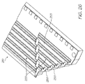
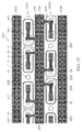
基板の上側面に配置され、印刷ヘッドに沿って長手方向に延びる1つまたは複数のノズル列に配列された複数のノズルアセンブリであって、それぞれが、上側面によって画定される床部を有するノズルチャンバと、床部から離間したルーフと、ルーフ内に画定されたノズル開口からインクを噴射するアクチュエータとを含む複数のノズルアセンブリと、
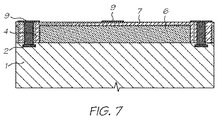
印刷ヘッド全体にわたって延び、ルーフを少なくとも部分的に画定するノズルプレートと、
ノズルプレートに配置された少なくとも1つの導電路であって、印刷ヘッドに沿って長手方向に、かつノズル列と平行に延びる少なくとも1つの導電路と、
を含み、
導電路は、駆動回路層と導電路との間に延びる複数の導体ポストを介して駆動回路層の共通基準面に接続される。
第1および第2の端子を有する上側熱弾性ビームと、
電流が熱弾性ビームを流れた場合に、熱弾性ビームが膨張し、その結果、それぞれのパドルがノズルチャンバの床部に向かって曲がるように熱弾性ビームに融着された下側受動ビームと、
を含む。
アクチュエータがドレーンと接地面との間に接続されるp型FETか、または
アクチュエータが電源面とソースとの間に接続されるn形FETか、
のいずれか一方である。
駆動回路層を含む基板と、
基板の上側面に配置され、印刷ヘッドICに沿って長手方向に延びる1つまたは複数のノズル列に配列された複数のノズルアセンブリであって、それぞれが、上側面によって画定される床部を有するノズルチャンバと、床部から離間したルーフと、ルーフ内に画定されたノズル開口からインクを噴射するアクチュエータとを含む複数のノズルアセンブリと、
印刷ヘッドIC全体にわたって延び、ルーフを少なくとも部分的に画定するノズルプレートと、
ノズルプレートに融着された少なくとも1つの導電路であって、印刷ヘッドに沿って長手方向に、かつノズル列と平行に延びる少なくとも1つの導電路と、
を含み、
導電路は、駆動回路層と導電路との間に延びる複数の導体ポストを介して駆動回路層の共通基準面に接続される。
完全を期すために、および背景的情報として、熱曲がりアクチュエータを有する可動ルーフパドルを含むインクジェットノズルアセンブリ(または「ノズル」)を製造するプロセスについて以下に説明する。図15および図16に示す完成したインクジェットノズルアセンブリ100は熱曲がり作用を利用し、それにより、ノズルチャンバルーフの可動パドル4が基板1に向かって曲がり、結果的にインクが噴射される。この製造プロセスは、本出願人が前に出願した米国特許出願公開第2008/0309728号明細書および同第2008/0225077号明細書に説明されており、これら特許の内容は、参照により本明細書に援用される。しかし、当然のことながら、相当する製造プロセスを使用して、本明細書で説明する任意のインクジェットノズルアセンブリ、実際には、印刷ヘッドおよび印刷ヘッド集積回路(IC)を製造することができる。
図12に最もよく示すとおり、本出願人が前述したインクジェットノズルアセンブリは、インクをノズル開口13から噴射するための1つの可動パドル14を含む。
図17および図18に示すノズルアセンブリ200、210は、滴の噴射方向を1つの軸に沿って制御するのを可能にする。通常(および最も有用には)、この軸は、長いページ幅印刷ヘッドの長手軸であり、ノズル列はこの長手軸に沿って延びる。しかし、ノズル開口に対して配置された3つ以上のパドルの使用を通じて、滴の方向性をそれ以上に制御することが可能である。
典型的なページ幅印刷ヘッドでは、各発射ノズル(すなわち、印刷ヘッドが受け取った印刷データに基づいて発射するように選択されたノズル)は、1ライン時間内に一度に発射する。さらに、各ノズルは、インク滴がノズルに対応する主ドット位置に載るようにインク滴を噴射する。ノズルがその対応する主ドット位置に噴射する場合、滴の噴射は、通常、印刷ヘッドのインク噴射面に対して垂直である。したがって、従来のページ幅印刷ヘッドでは、印刷ヘッドのノズル密度は印刷されたページのドット密度に一致する。例えば、ノズルピッチがnのページ幅ノズル列は、ドットピッチがnのドットラインを印刷し、ノズルピッチおよびドットピッチは、それぞれ隣接するノズルおよびドットの図心間の距離として定義される。
本出願人は、静止ページ幅印刷ヘッドの故障ノズル補償を行うための機構についてすでに説明した。本明細書では、「故障ノズル」とは、全くインクを噴射しないノズル、または滴の速度もしくは滴の方向性を十分に制御することなくインクを噴射するノズルを意味する。通常、「故障ノズル」は、(検出回路によって最も容易に特定可能なノズル不良の原因である)アクチュエータ不良によって引き起こされるが、ノズル開口内の取り除くことのできない妨害物、またはノズル開口を覆う、もしくは部分的に覆う、インク噴射面上の取り除くことのできない異物によっても引き起こされる。
非常に低い歩留まりを欠点としてもつ一体構造のページ幅印刷ヘッドを除いて、本出願人によるページ幅印刷ヘッドは通常、ページ幅全体にわたって、複数の印刷ヘッドICの端部同士を合わせて接合することで構築される。
MEMS印刷ヘッド構造に関する重要な態様として、MEMSアクチュエータと下にあるCMOS駆動回路との統合がある。ノズルを作動させるために、CMOS駆動回路層の駆動トランジスタからの電流は上方に流れてMEMS層に入り、アクチュエータを通り、下降してCMOS駆動回路層に(例えば、CMOS層の接地面に)戻らなければならない。1つの印刷ヘッドICに数千のアクチュエータがある場合、電流の流路の効率は、印刷ヘッド全体の効率の低下を最小限にするように最大化されるべきである。
Claims (10)
- 駆動回路層を含む基板と、
前記基板の上側面に配置され、印刷ヘッドに沿って長手方向に延びる1つまたは複数のノズル列に配列された複数のノズルアセンブリであって、各ノズルアセンブリが、前記上側面によって画定された床部を有するノズルチャンバと、前記床部から離間したルーフと、前記ルーフ内に画定されたノズル開口からインクを噴射するアクチュエータとを含む複数のノズルアセンブリと、
前記印刷ヘッド全体にわたって延び、前記ルーフを含むノズルプレートと、
前記ノズルプレートに配置された少なくとも1つの導電路であって、前記印刷ヘッドに沿って長手方向に、かつ前記ノズル列と平行に延びる少なくとも1つの導電路と、
を含むインクジェット印刷ヘッドにおいて、前記導電路は、前記駆動回路層と前記導電路との間に延びる複数の導体ポストを介して、前記駆動回路層の共通基準面に接続されることを特徴とするインクジェット印刷ヘッド。 - 請求項1に記載のインクジェット印刷ヘッドにおいて、前記共通基準面は、接地面または電源面を画定することを特徴とするインクジェット印刷ヘッド。
- 請求項1に記載のインクジェット印刷ヘッドにおいて、少なくとも1つの第1の導電路を含み、前記第1の導電路は、前記第1の導電路に隣接する少なくとも1つのノズル列の複数のアクチュエータに直接接続されることを特徴とするインクジェット印刷ヘッド。
- 請求項3に記載のインクジェット印刷ヘッドにおいて、少なくとも1つの第2の導電路をさらに含み、前記第2の導電路は、いずれのアクチュエータにも直接接続されないことを特徴とするインクジェット印刷ヘッド。
- 請求項3に記載のインクジェット印刷ヘッドにおいて、前記第1の導電路は、前記ノズル列の各アクチュエータ用の共通基準面を形成するように、前記印刷ヘッドに沿って連続的に延びることを特徴とするインクジェット印刷ヘッド。
- 請求項3に記載のインクジェット印刷ヘッドにおいて、前記第1の導電路は、前記ノズル列のアクチュエータセット用の共通基準面を形成するように、前記印刷ヘッドに沿って不連続に延びることを特徴とするインクジェット印刷ヘッド。
- 請求項3に記載のインクジェット印刷ヘッドにおいて、前記第1の導電路は、それぞれのノズル列対間に配置され、前記第1の導電路は、前記対のノズル列の両方の複数のアクチュエータ用の共通基準面を形成することを特徴とするインクジェット印刷ヘッド。
- 請求項3に記載のインクジェット印刷ヘッドにおいて、各アクチュエータは、前記第1の導電路に直接接続された第1の端子と、前記駆動回路層の駆動トランジスタに接続された第2の端子とを有することを特徴とするインクジェット印刷ヘッド。
- 請求項8に記載のインクジェット印刷ヘッドにおいて、各ルーフは、少なくとも1つのアクチュエータを含み、各アクチュエータの前記第1の端子は、前記ノズルプレート全体にわたって、前記第1の導電路に対して横方向に延びる横接続体を介して前記第1の導電路に接続されることを特徴とするインクジェット印刷ヘッド。
- 請求項9に記載のインクジェット印刷ヘッドにおいて、前記第2の端子は、前記駆動回路層と前記第2の端子との間に延びるアクチュエータポストを介して前記駆動トランジスタに接続されることを特徴とするインクジェット印刷ヘッド。
Applications Claiming Priority (1)
| Application Number | Priority Date | Filing Date | Title |
|---|---|---|---|
| PCT/AU2010/001292 WO2012040765A1 (en) | 2010-10-01 | 2010-10-01 | Inkjet printhead having common conductive track on nozzle plate |
Related Child Applications (1)
| Application Number | Title | Priority Date | Filing Date |
|---|---|---|---|
| JP2015016256A Division JP2015110340A (ja) | 2015-01-30 | 2015-01-30 | 独立して動作可能なルーフパドルによる滴方向制御を伴うインクジェットノズルアセンブリ |
Publications (3)
| Publication Number | Publication Date |
|---|---|
| JP2013538711A JP2013538711A (ja) | 2013-10-17 |
| JP2013538711A5 JP2013538711A5 (ja) | 2013-11-28 |
| JP5692881B2 true JP5692881B2 (ja) | 2015-04-01 |
Family
ID=45891710
Family Applications (1)
| Application Number | Title | Priority Date | Filing Date |
|---|---|---|---|
| JP2013530490A Active JP5692881B2 (ja) | 2010-10-01 | 2010-10-01 | ノズルプレートに共通導電路を有するインクジェット印刷ヘッド |
Country Status (7)
| Country | Link |
|---|---|
| EP (1) | EP2621728B1 (ja) |
| JP (1) | JP5692881B2 (ja) |
| KR (1) | KR101723262B1 (ja) |
| CN (1) | CN103370201B (ja) |
| AU (1) | AU2010361609B2 (ja) |
| SG (1) | SG189013A1 (ja) |
| WO (1) | WO2012040765A1 (ja) |
Families Citing this family (2)
| Publication number | Priority date | Publication date | Assignee | Title |
|---|---|---|---|---|
| GB2539052B (en) * | 2015-06-05 | 2020-01-01 | Xaar Technology Ltd | Inkjet printhead |
| US20220242116A1 (en) * | 2019-07-17 | 2022-08-04 | Scrona Ag | Electrohydrodynamic print head with structured feed layer |
Family Cites Families (13)
| Publication number | Priority date | Publication date | Assignee | Title |
|---|---|---|---|---|
| EP0772525A1 (en) * | 1995-04-12 | 1997-05-14 | Eastman Kodak Company | Constructions and manufacturing processes for thermally activated print heads |
| US6648453B2 (en) * | 1997-07-15 | 2003-11-18 | Silverbrook Research Pty Ltd | Ink jet printhead chip with predetermined micro-electromechanical systems height |
| US6623108B2 (en) * | 1998-10-16 | 2003-09-23 | Silverbrook Research Pty Ltd | Ink jet printhead having thermal bend actuator heating element electrically isolated from nozzle chamber ink |
| US6265301B1 (en) * | 1999-05-12 | 2001-07-24 | Taiwan Semiconductor Manufacturing Company | Method of forming metal interconnect structures and metal via structures using photolithographic and electroplating or electro-less plating procedures |
| US6938993B2 (en) | 2002-10-31 | 2005-09-06 | Benq Corporation | Fluid injection head structure |
| JP3972363B2 (ja) * | 2003-06-11 | 2007-09-05 | ソニー株式会社 | 液体吐出装置及び液体吐出方法 |
| JP4537159B2 (ja) * | 2003-09-08 | 2010-09-01 | キヤノン株式会社 | 液体吐出ヘッド用半導体装置、液体吐出へッド及び液体吐出装置 |
| US7252353B2 (en) | 2004-05-27 | 2007-08-07 | Silverbrook Research Pty Ltd | Printer controller for supplying data to a printhead module having one or more redundant nozzle rows |
| TWI253395B (en) * | 2005-01-13 | 2006-04-21 | Benq Corp | Fluid injector |
| US7465017B2 (en) | 2005-12-05 | 2008-12-16 | Silverbrook Research Pty Ltd | Dot-at-a-time redundancy for modulating printhead peak power requirement |
| JP2008044310A (ja) * | 2006-08-21 | 2008-02-28 | Canon Inc | インクジェット記録ヘッド |
| US7866795B2 (en) * | 2007-06-15 | 2011-01-11 | Silverbrook Research Pty Ltd | Method of forming connection between electrode and actuator in an inkjet nozzle assembly |
| US8226213B2 (en) * | 2008-05-05 | 2012-07-24 | Zamtec Limited | Short pulsewidth actuation of thermal bend actuator |
-
2010
- 2010-10-01 KR KR1020137010958A patent/KR101723262B1/ko active IP Right Grant
- 2010-10-01 AU AU2010361609A patent/AU2010361609B2/en not_active Ceased
- 2010-10-01 WO PCT/AU2010/001292 patent/WO2012040765A1/en active Application Filing
- 2010-10-01 SG SG2013019849A patent/SG189013A1/en unknown
- 2010-10-01 CN CN201080070167.5A patent/CN103370201B/zh active Active
- 2010-10-01 EP EP10857627.3A patent/EP2621728B1/en active Active
- 2010-10-01 JP JP2013530490A patent/JP5692881B2/ja active Active
Also Published As
| Publication number | Publication date |
|---|---|
| SG189013A1 (en) | 2013-05-31 |
| EP2621728A1 (en) | 2013-08-07 |
| AU2010361609B2 (en) | 2014-08-14 |
| AU2010361609A1 (en) | 2013-03-21 |
| KR101723262B1 (ko) | 2017-04-04 |
| EP2621728B1 (en) | 2019-02-13 |
| EP2621728A4 (en) | 2015-05-27 |
| JP2013538711A (ja) | 2013-10-17 |
| CN103370201A (zh) | 2013-10-23 |
| WO2012040765A1 (en) | 2012-04-05 |
| CN103370201B (zh) | 2015-07-15 |
| KR20130141499A (ko) | 2013-12-26 |
Similar Documents
| Publication | Publication Date | Title |
|---|---|---|
| JP2006123551A (ja) | ノズルプレートとそれを備えたインクジェットプリントヘッド及びノズルプレートの製造方法 | |
| CN1328052C (zh) | 包括可移动推墨器的喷墨打印头芯片 | |
| KR101444560B1 (ko) | 배면의 전기접속부를 갖는 잉크젯 프린트헤드 조립체 | |
| US8485623B2 (en) | Pagewidth inkjet printhead configured such that printed dot density exceeds nozzle density | |
| US8388111B2 (en) | Method of printing at dot density exceeding nozzle density in stationary pagewidth printhead | |
| US8714677B2 (en) | Inkjet printhead with join regions seamlessly compensated by directional nozzles | |
| US8434844B2 (en) | Stationary inkjet printhead with dead nozzle compensation provided by nozzles in same nozzles row | |
| JP5692881B2 (ja) | ノズルプレートに共通導電路を有するインクジェット印刷ヘッド | |
| JP2015110340A (ja) | 独立して動作可能なルーフパドルによる滴方向制御を伴うインクジェットノズルアセンブリ | |
| US8353577B2 (en) | Method of controlling drop directionality from inkjet nozzle using multiple independently-actuable roof paddles | |
| US8506052B2 (en) | Inkjet nozzle assembly with drop directionality control via independently actuable roof paddles | |
| US8356884B2 (en) | Printhead integrated circuit having common conductive track fused to nozzle plate | |
| US8485638B2 (en) | Inkjet printhead having common conductive track on nozzle plate | |
| AU2014262188B2 (en) | Inkjet nozzle assembly with drop directionality control via independently actuable roof paddles | |
| US8529005B2 (en) | Method of compensating for dead nozzles in stationary pagewidth printhead | |
| US8540344B2 (en) | Pagewidth inkjet printhead with drop directionality control | |
| US8342643B2 (en) | Printhead integrated circuit with end nozzles firing at multiple dot positions | |
| US8348388B2 (en) | Printhead integrated circuit with printable zone longer than nozzle row | |
| CN105058985A (zh) | 通过可独立致动的腔顶桨状物控制墨滴方向性的喷墨喷嘴组件 | |
| TWI499514B (zh) | 藉由可獨立致動的頂壁漿片而具有液滴方向控制的噴墨噴嘴組件 | |
| TWI525001B (zh) | 具有共同導電跡線於噴嘴板上的噴墨列印頭 | |
| CN111703207B (zh) | 带单层内电极的压电喷墨打印器件 | |
| WO2012040766A1 (en) | Inkjet nozzle assembly with drop directionality control via independently actuable roof paddles |
Legal Events
| Date | Code | Title | Description |
|---|---|---|---|
| A521 | Request for written amendment filed |
Free format text: JAPANESE INTERMEDIATE CODE: A523 Effective date: 20131001 |
|
| A621 | Written request for application examination |
Free format text: JAPANESE INTERMEDIATE CODE: A621 Effective date: 20131001 |
|
| A977 | Report on retrieval |
Free format text: JAPANESE INTERMEDIATE CODE: A971007 Effective date: 20140227 |
|
| A131 | Notification of reasons for refusal |
Free format text: JAPANESE INTERMEDIATE CODE: A131 Effective date: 20140304 |
|
| A521 | Request for written amendment filed |
Free format text: JAPANESE INTERMEDIATE CODE: A523 Effective date: 20140528 |
|
| TRDD | Decision of grant or rejection written | ||
| A01 | Written decision to grant a patent or to grant a registration (utility model) |
Free format text: JAPANESE INTERMEDIATE CODE: A01 Effective date: 20150120 |
|
| A61 | First payment of annual fees (during grant procedure) |
Free format text: JAPANESE INTERMEDIATE CODE: A61 Effective date: 20150130 |
|
| R150 | Certificate of patent or registration of utility model |
Ref document number: 5692881 Country of ref document: JP Free format text: JAPANESE INTERMEDIATE CODE: R150 |
|
| R250 | Receipt of annual fees |
Free format text: JAPANESE INTERMEDIATE CODE: R250 |
|
| R250 | Receipt of annual fees |
Free format text: JAPANESE INTERMEDIATE CODE: R250 |
|
| R250 | Receipt of annual fees |
Free format text: JAPANESE INTERMEDIATE CODE: R250 |
|
| R250 | Receipt of annual fees |
Free format text: JAPANESE INTERMEDIATE CODE: R250 |
|
| R250 | Receipt of annual fees |
Free format text: JAPANESE INTERMEDIATE CODE: R250 |
|
| R250 | Receipt of annual fees |
Free format text: JAPANESE INTERMEDIATE CODE: R250 |
|
| R250 | Receipt of annual fees |
Free format text: JAPANESE INTERMEDIATE CODE: R250 |