EP2615891A1 - Method for surface mounting electronic component, and substrate having electronic component mounted thereon - Google Patents
Method for surface mounting electronic component, and substrate having electronic component mounted thereon Download PDFInfo
- Publication number
- EP2615891A1 EP2615891A1 EP11823319.6A EP11823319A EP2615891A1 EP 2615891 A1 EP2615891 A1 EP 2615891A1 EP 11823319 A EP11823319 A EP 11823319A EP 2615891 A1 EP2615891 A1 EP 2615891A1
- Authority
- EP
- European Patent Office
- Prior art keywords
- electronic component
- metal layer
- conductive circuit
- thermoplastic resin
- electrode
- Prior art date
- Legal status (The legal status is an assumption and is not a legal conclusion. Google has not performed a legal analysis and makes no representation as to the accuracy of the status listed.)
- Withdrawn
Links
Images




Classifications
-
- H—ELECTRICITY
- H01—ELECTRIC ELEMENTS
- H01G—CAPACITORS; CAPACITORS, RECTIFIERS, DETECTORS, SWITCHING DEVICES, LIGHT-SENSITIVE OR TEMPERATURE-SENSITIVE DEVICES OF THE ELECTROLYTIC TYPE
- H01G2/00—Details of capacitors not covered by a single one of groups H01G4/00-H01G11/00
- H01G2/02—Mountings
- H01G2/06—Mountings specially adapted for mounting on a printed-circuit support
-
- B—PERFORMING OPERATIONS; TRANSPORTING
- B32—LAYERED PRODUCTS
- B32B—LAYERED PRODUCTS, i.e. PRODUCTS BUILT-UP OF STRATA OF FLAT OR NON-FLAT, e.g. CELLULAR OR HONEYCOMB, FORM
- B32B37/00—Methods or apparatus for laminating, e.g. by curing or by ultrasonic bonding
- B32B37/04—Methods or apparatus for laminating, e.g. by curing or by ultrasonic bonding characterised by the partial melting of at least one layer
-
- H—ELECTRICITY
- H01—ELECTRIC ELEMENTS
- H01G—CAPACITORS; CAPACITORS, RECTIFIERS, DETECTORS, SWITCHING DEVICES, LIGHT-SENSITIVE OR TEMPERATURE-SENSITIVE DEVICES OF THE ELECTROLYTIC TYPE
- H01G4/00—Fixed capacitors; Processes of their manufacture
- H01G4/002—Details
- H01G4/228—Terminals
-
- H—ELECTRICITY
- H05—ELECTRIC TECHNIQUES NOT OTHERWISE PROVIDED FOR
- H05K—PRINTED CIRCUITS; CASINGS OR CONSTRUCTIONAL DETAILS OF ELECTRIC APPARATUS; MANUFACTURE OF ASSEMBLAGES OF ELECTRICAL COMPONENTS
- H05K1/00—Printed circuits
- H05K1/02—Details
- H05K1/11—Printed elements for providing electric connections to or between printed circuits
-
- H—ELECTRICITY
- H05—ELECTRIC TECHNIQUES NOT OTHERWISE PROVIDED FOR
- H05K—PRINTED CIRCUITS; CASINGS OR CONSTRUCTIONAL DETAILS OF ELECTRIC APPARATUS; MANUFACTURE OF ASSEMBLAGES OF ELECTRICAL COMPONENTS
- H05K3/00—Apparatus or processes for manufacturing printed circuits
- H05K3/30—Assembling printed circuits with electric components, e.g. with resistors
- H05K3/303—Assembling printed circuits with electric components, e.g. with resistors with surface mounted components
- H05K3/305—Affixing by adhesive
-
- H—ELECTRICITY
- H05—ELECTRIC TECHNIQUES NOT OTHERWISE PROVIDED FOR
- H05K—PRINTED CIRCUITS; CASINGS OR CONSTRUCTIONAL DETAILS OF ELECTRIC APPARATUS; MANUFACTURE OF ASSEMBLAGES OF ELECTRICAL COMPONENTS
- H05K3/00—Apparatus or processes for manufacturing printed circuits
- H05K3/30—Assembling printed circuits with electric components, e.g. with resistors
- H05K3/32—Assembling printed circuits with electric components, e.g. with resistors electrically connecting electric components or wires to printed circuits
-
- H—ELECTRICITY
- H05—ELECTRIC TECHNIQUES NOT OTHERWISE PROVIDED FOR
- H05K—PRINTED CIRCUITS; CASINGS OR CONSTRUCTIONAL DETAILS OF ELECTRIC APPARATUS; MANUFACTURE OF ASSEMBLAGES OF ELECTRICAL COMPONENTS
- H05K2201/00—Indexing scheme relating to printed circuits covered by H05K1/00
- H05K2201/01—Dielectrics
- H05K2201/0104—Properties and characteristics in general
- H05K2201/0129—Thermoplastic polymer, e.g. auto-adhesive layer; Shaping of thermoplastic polymer
-
- H—ELECTRICITY
- H05—ELECTRIC TECHNIQUES NOT OTHERWISE PROVIDED FOR
- H05K—PRINTED CIRCUITS; CASINGS OR CONSTRUCTIONAL DETAILS OF ELECTRIC APPARATUS; MANUFACTURE OF ASSEMBLAGES OF ELECTRICAL COMPONENTS
- H05K2201/00—Indexing scheme relating to printed circuits covered by H05K1/00
- H05K2201/10—Details of components or other objects attached to or integrated in a printed circuit board
- H05K2201/10613—Details of electrical connections of non-printed components, e.g. special leads
- H05K2201/10621—Components characterised by their electrical contacts
- H05K2201/10636—Leadless chip, e.g. chip capacitor or resistor
-
- H—ELECTRICITY
- H05—ELECTRIC TECHNIQUES NOT OTHERWISE PROVIDED FOR
- H05K—PRINTED CIRCUITS; CASINGS OR CONSTRUCTIONAL DETAILS OF ELECTRIC APPARATUS; MANUFACTURE OF ASSEMBLAGES OF ELECTRICAL COMPONENTS
- H05K2203/00—Indexing scheme relating to apparatus or processes for manufacturing printed circuits covered by H05K3/00
- H05K2203/02—Details related to mechanical or acoustic processing, e.g. drilling, punching, cutting, using ultrasound
- H05K2203/0285—Using ultrasound, e.g. for cleaning, soldering or wet treatment
-
- H—ELECTRICITY
- H05—ELECTRIC TECHNIQUES NOT OTHERWISE PROVIDED FOR
- H05K—PRINTED CIRCUITS; CASINGS OR CONSTRUCTIONAL DETAILS OF ELECTRIC APPARATUS; MANUFACTURE OF ASSEMBLAGES OF ELECTRICAL COMPONENTS
- H05K2203/00—Indexing scheme relating to apparatus or processes for manufacturing printed circuits covered by H05K3/00
- H05K2203/05—Patterning and lithography; Masks; Details of resist
- H05K2203/0562—Details of resist
- H05K2203/0571—Dual purpose resist, e.g. etch resist used as solder resist, solder resist used as plating resist
-
- H—ELECTRICITY
- H05—ELECTRIC TECHNIQUES NOT OTHERWISE PROVIDED FOR
- H05K—PRINTED CIRCUITS; CASINGS OR CONSTRUCTIONAL DETAILS OF ELECTRIC APPARATUS; MANUFACTURE OF ASSEMBLAGES OF ELECTRICAL COMPONENTS
- H05K2203/00—Indexing scheme relating to apparatus or processes for manufacturing printed circuits covered by H05K3/00
- H05K2203/11—Treatments characterised by their effect, e.g. heating, cooling, roughening
- H05K2203/1189—Pressing leads, bumps or a die through an insulating layer
-
- H—ELECTRICITY
- H05—ELECTRIC TECHNIQUES NOT OTHERWISE PROVIDED FOR
- H05K—PRINTED CIRCUITS; CASINGS OR CONSTRUCTIONAL DETAILS OF ELECTRIC APPARATUS; MANUFACTURE OF ASSEMBLAGES OF ELECTRICAL COMPONENTS
- H05K2203/00—Indexing scheme relating to apparatus or processes for manufacturing printed circuits covered by H05K3/00
- H05K2203/14—Related to the order of processing steps
- H05K2203/1461—Applying or finishing the circuit pattern after another process, e.g. after filling of vias with conductive paste, after making printed resistors
-
- H—ELECTRICITY
- H05—ELECTRIC TECHNIQUES NOT OTHERWISE PROVIDED FOR
- H05K—PRINTED CIRCUITS; CASINGS OR CONSTRUCTIONAL DETAILS OF ELECTRIC APPARATUS; MANUFACTURE OF ASSEMBLAGES OF ELECTRICAL COMPONENTS
- H05K3/00—Apparatus or processes for manufacturing printed circuits
- H05K3/02—Apparatus or processes for manufacturing printed circuits in which the conductive material is applied to the surface of the insulating support and is thereafter removed from such areas of the surface which are not intended for current conducting or shielding
- H05K3/06—Apparatus or processes for manufacturing printed circuits in which the conductive material is applied to the surface of the insulating support and is thereafter removed from such areas of the surface which are not intended for current conducting or shielding the conductive material being removed chemically or electrolytically, e.g. by photo-etch process
-
- H—ELECTRICITY
- H05—ELECTRIC TECHNIQUES NOT OTHERWISE PROVIDED FOR
- H05K—PRINTED CIRCUITS; CASINGS OR CONSTRUCTIONAL DETAILS OF ELECTRIC APPARATUS; MANUFACTURE OF ASSEMBLAGES OF ELECTRICAL COMPONENTS
- H05K3/00—Apparatus or processes for manufacturing printed circuits
- H05K3/22—Secondary treatment of printed circuits
- H05K3/24—Reinforcing of the conductive pattern
- H05K3/244—Finish plating of conductors, especially of copper conductors, e.g. for pads or lands
-
- Y—GENERAL TAGGING OF NEW TECHNOLOGICAL DEVELOPMENTS; GENERAL TAGGING OF CROSS-SECTIONAL TECHNOLOGIES SPANNING OVER SEVERAL SECTIONS OF THE IPC; TECHNICAL SUBJECTS COVERED BY FORMER USPC CROSS-REFERENCE ART COLLECTIONS [XRACs] AND DIGESTS
- Y02—TECHNOLOGIES OR APPLICATIONS FOR MITIGATION OR ADAPTATION AGAINST CLIMATE CHANGE
- Y02P—CLIMATE CHANGE MITIGATION TECHNOLOGIES IN THE PRODUCTION OR PROCESSING OF GOODS
- Y02P70/00—Climate change mitigation technologies in the production process for final industrial or consumer products
- Y02P70/50—Manufacturing or production processes characterised by the final manufactured product
Definitions
- the present invention relates to a method for surface mounting an electronic component for surface mounting various types of electronic components such as a resistor or a capacitor on a printed wiring board on which a conductive circuit is formed, and a substrate having an electronic component mounted thereon.
- a copper foil 220 having a thickness of about 12 ⁇ m to 35 ⁇ m is laminated on a surface of a base material 210 made of a heat-resistant glass epoxy resin or polyimide resin, and this is used as a substrate (see Fig. 5(A) ).
- a conductive circuit 221 is formed on the substrate using a conventionally known photolithography method and etching method (see Fig. 5(B) ).
- a printed wiring board 200 is produced by applying plating 230 of Sn or the like to a position where an electronic component 300 is connected to impart wettability with a solder material (see Fig. 5(C) ).
- solder paste 240 is applied onto the plating 230 of the conductive circuit 221 by screen printing or the like. Then, an electrode 310 of the electronic component 300 is placed on the solder 240 (see Fig. 5(D) ). The solder 240 is heated and melted at a temperature of 260 to 270°C for several seconds while the electronic component 300 is placed, and is hardened by cooling after a fillet 241 is formed. Subsequently, a flux material in the solder 240 is removed by cleaning, so that mounting of the electronic component 300 onto the conductive circuit 221 is completed.
- Fig. 6 is a schematic cross sectional view of a substrate on which an electronic component is mounted, which is produced by a method for surface mounting according to Conventional Example 2.
- Fig. 7 is a process diagram illustrating surface mounting procedures according to Conventional Example 2.
- a metal foil 420 is laminated on a surface of an insulating base material 410 made of a glass epoxy resin or the like, and this is used as a substrate (see Fig. 7(A) ).
- a thermoplastic resin material hereinafter, referred to as "resist” formed as an ink material is coated on a surface of the substrate so as to form a predetermined pattern (see Fig. 7(B) ).
- a conductive circuit 421 is formed by etching and removing the metal of an exposed portion that is not covered with a resist 430. In this way, a printed wiring board 400 on which the conductive circuit 421 is formed can be provided (see Fig. 7(C) ).
- a protruding electrode 450 is formed by plating, a stud bump method which is conventionally known, or the like on a surface of an electrode 510 of an electronic component 500 (see Fig. 7(D) ).
- the electronic component 500 is pressed onto the resist 430, which is heated at a temperature of about 60°C, on a surface of the printed wiring board 400 so that the protruding electrode 450 makes contact therewith while ultrasonic vibration is applied (see Fig. 7(E) ).
- a portion of the resist 430 to which a tip end of the protruding electrode 450 is pressed melts and is removed by friction caused between the protruding electrode 450 and the resist 430.
- a metal fused portion 460 is formed by friction caused by the ultrasonic vibration between the tip end of the protruding electrode 450 and the conductive circuit 421.
- the resist 430 made of a thermoplastic resin is cooled and hardened again by stopping the ultrasonic vibration, and the electrode 510 of the electronic component 500 and the conductive circuit 421 are electrically connected to each other through the protruding electrode 450 and the metal fused portion 460 (see Fig. 7(F) and Fig. 6 ).
- the mechanism of bonding utilizing the ultrasonic vibration involves occurrences of relative sliding friction of a joint interface, destruction of a surface oxide film, metallic diffusion, and completion of bonding, in this order.
- the flow of these sequences does not take place in an entire joint interface simultaneously, but there is a case where even a portion in which bonding is completed is continuously subjected to a load generated by the ultrasonic vibration.
- the stress caused by the ultrasonic vibration cannot be fled through interface slip, and a shear stress is exerted on the bonded portion. Accordingly, cracks tend to be caused near the bonded portion, because, generally, the welded portion has a large deformation strength.
- a first method for surface mounting an electronic component includes the steps of: providing, on a substrate member, a conductive circuit, and a thermoplastic resin layer which is formed on a front surface of the conductive circuit; providing a surface of an electrode of an electronic component with a metal layer; and bonding the metal layer of the electronic component and the conductive circuit to each other by melting and then partially removing a thermoplastic resin by applying a load generated by ultrasonic vibration that vibrates in a direction substantially parallel to a surface of the metal layer, while pressing the metal layer to the thermoplastic resin layer, and then stopping applying the load generated by the ultrasonic vibration, and hardening the thermoplastic resin thus melted by cooling.
- the metal layer is configured by a thin layer made of a material having a shear strength lower than that of a material constituting the conductive circuit.
- the metal layer is configured by a thin layer made of a material having a shear strength lower than that of a material constituting the conductive circuit. Accordingly, it is possible to suppress breakage of the conductive circuit even in the case where a load generated by the ultrasonic vibration is applied.
- first bonded portion for convenient sake
- second bonded portion for convenient sake
- the thickness (this corresponds to the thickness of the layer of the metal layer in the case of this embodiment, or a protruding amount in the case of the protruding electrode) can be reduced, the stress moment caused between the first bonded portion and the second bonded portion can be reduced, and therefore the shear stress in each of the bonded portions can be reduced.
- a larger elastic deformation area is provided, the ductility is increased, and therefore it is easy to absorb the shear stress.
- breakage of the conductive circuit is deterred, the load caused by the shear stress exerted on each bonded portion can be suppressed, and therefore it is possible to suppress the occurrence of cracks in the joint interface.
- the second invention is directed to a method for surface mounting an electronic component, including the steps of: providing, on a substrate member, a conductive circuit, and a metal layer which is formed on a front surface of the conductive circuit; providing a front surface of the metal layer with a thermoplastic resin layer; and bonding an electrode of an electronic component and the metal layer to each other by melting and partially removing a thermoplastic resin by applying a load generated by ultrasonic vibration that vibrates in a direction substantially parallel to a surface of the electrode, while pressing the surface of the electrode to the thermoplastic resin layer, and then stopping applying the load generated by the ultrasonic vibration, and hardening the thermoplastic resin thus melted by cooling.
- the metal layer is configured by a thin layer made of a material having a shear strength lower than that of a material constituting the conductive circuit.
- the electronic component is mounted on a substrate member by any one of the methods for surface mounting an electronic component described above.
- a substrate having an electronic component produced by a method for surface mounting an electronic component according to Embodiment 1 of the present invention will be described.
- a substrate 100 having an electronic component mounted thereon includes an insulating base material 10 as a substrate member, a conductive circuit 21 formed on a surface of the insulating base material 10, and metal layers 50 provided on a pair of electrodes 41 of an electronic component 40 and fixed while being electrically connected to the conductive circuit 21. Further, the substrate 100 is also provided with a resin fixing portion 31 that functions to further reinforce fixing between the insulating base material 10 and the electronic component 40.
- a glass epoxy resin is named as a preferred example as a material of the insulating base material 10.
- various types of electronic components that can be mounted by surface mounting such as a resistor and a capacitor, are applied as the electronic component 40.
- a metal foil 20 is laminated on a surface of the insulating base material 10 (see Fig. 2(A) ).
- the metal foil 20 made of hard aluminum having a thickness of 35 ⁇ m is placed on one side of the insulating base material (Garaepoprepreg) 10 made of glass epoxy having a thickness of 50 ⁇ m, which are joined together by hot press. Since this bonding method is a publicly known technique, and the detailed description thereof will be omitted.
- the insulating base material 10 including the metal foil 20 laminated on a surface thereof can be obtained.
- a copper foil having a thickness of 18 ⁇ m is named as another specific example of the metal foil 20.
- a desired pattern shape (shape of the conductive circuit) of a resist 30 is formed on a surface of the metal foil 20 by an ink material made of a thermoplastic resin (see Fig. 2(B) ).
- a desired pattern shape of the resist 30 is formed on the surface of the metal foil 20 by a polyolefin thermoplastic adhesive or the like which melts at a temperature of about 150°C.
- the resist 30 is formed by coating to a thickness of about 2 to 3 ⁇ m by a method such as gravure printing.
- the metal foil 20 in an exposed position which is not covered with the resist 30 is removed by etching to thereby form the conductive circuit 21.
- a surface of this conductive circuit 21 is covered with the resist 30 serving as a thermoplastic resin layer (see Fig. 2(C) ).
- etching process it is preferable to use NaOH (120 g/l) as an etchant at a temperature condition of 50°C.
- a polyester plastic resin instead of the polyolefin thermoplastic resin which is used for the resist 30.
- FeCl 2 of an acid system is used as the etchant during etching.
- an area of the bonded portion of the conductive circuit 21 can be made smaller than an area of the bonded portion of the electrode 41 of the electronic component 40. For this reason, the area of the bonded portion of the conductive circuit 21 can be made smaller as compared with the conventional method for mounting using a solder material (e.g., in the case of a chip capacitor having a size of 1.0 mm by 0.5 mm, an area about a twice an electrode area is necessary).
- a metal layer 50 serving as a thin layer having a thickness of about 1 ⁇ m is formed, by plating or the like, on an entire surface on a side to be joined of the electrode 41 of the electronic component 40 (see Fig. 2(D) ).
- a material used to form the metal layer 50 is a material having a shear strength (shearing resistance) smaller than that of a material constituting the conductive circuit 21.
- both surfaces of the metal layer 50 are formed to have flat surfaces.
- the metal layer 50 is formed to have a thickness of about 1 ⁇ m by a conventional gold plating method using gold having a shear strength of 1600 kg/cm 2 on an entire surface on a side to be joined to the conductive circuit 21, and this is applied to each of the pair of electrodes 41 of a chip capacitor (electronic component 40) having a size of 1.0 mm by 0.5 mm.
- the shear strength is about 2000 to 3000 kg/cm 2 , and about 3000 kg/cm 2 or more when it is formed of copper. Accordingly, in any of the cases, the shear strength of the metal layer 50 is lower than the shear strength of the conductive circuit 21.
- the metal layer 50 is provided only on a surface of the electrode 41 on a side to be joined to the conductive circuit 21.
- a load generated by ultrasonic vibration vibrating in a direction substantially parallel to a surface of the metal layer 50 is applied while the metal layer 50 provided on the surface of the electrode 41 of the electronic component 40 is pressed against the resist 30 serving as the thermoplastic resin layer (see Fig. 2(E) ).
- This process is performed while the insulating base material 10 having the conductive circuit 21 on which the resist 30 is formed is heated to a temperature of about 60°C.
- a part of the resist 30 formed of the thermoplastic resin is removed from the surface of the conductive circuit 21 by mechanical friction caused by the ultrasonic vibration.
- a part of the resist 30 melts by frictional heat, and the resin that is melted by pressure is pushed away in a direction perpendicular to a direction in which the pressure is exerted and removed from a region between the surface of the metal layer 50 and the surface of the conductive circuit 21.
- an oxide layer on the surface of the conductive circuit 21 is also mechanically removed so that the surface of the metal layer 50 on the electrode 41 makes contact with the surface of the conductive circuit 21. Furthermore, a metal fused portion is formed between these surfaces by the friction caused by the ultrasonic vibration.
- thermoplastic resin that has been melted by heat is hardened again by cooling.
- the resin fixing portion 31 exerting a function of reinforcing the fixing between the insulating base material 10 and the electronic component 40 is formed (see Fig. 2(F) ).
- the load generated by the ultrasonic vibration at a vibration frequency of 63 kHz is applied while the metal layer 50 provided on the electrode 41 of the chip capacitor (electronic component 40) is pressed against the resist 30 under the condition of a pressure of 0.2 kg/mm 2 .
- the material of the metal layer 50 is not limited to gold.
- a material having conductivity, and a shear strength (shearing resistance) smaller than that of a material constituting the conductive circuit 21 may serve as the material of the metal layer 50. Accordingly, other than gold, aluminum, zinc, nickel, copper, or an alloy made by arbitrarily combining these, or the like can be used according to the material that constitutes the conductive circuit 21.
- the material made of glass epoxy having a thickness of 50 ⁇ m is described.
- the material and the thickness of the insulating base material 10 are not limited to this example.
- the method does not provide a problem such as a disconnection of line or short-circuiting caused by insufficient supply or protrusion of the solder material, and therefore the area of the conductive circuit 21 can be made smaller. There is no need to form a fillet for securing a reliability in solder bonding, and therefore the area of the conductive circuit 21 can be made smaller.
- the method does not provide a problem of wettability of materials constituting the solder material and the conductive circuit 21, and therefore the cost for material can be reduced because plating on the surface of the conductive circuit 21 can be eliminated, inexpensive aluminum can be employed as a material of the conductive circuit 21, and the like.
- Heat treatment for melting the solder material is not necessary, and therefore an inexpensive low heat resistant material such as PET (polyethylene terephthalate) can be used as a material for the base material (insulating base material 10) of the printed wiring board.
- PET polyethylene terephthalate
- a further reduction in manufacturing cost is possible.
- the metal layer 50 provided on the surface of the electronic component 40 is formed of a thin layer (a layer having a flat surface on a side of the conductive circuit 21) made of a material having a shear strength smaller than that of the material constituting the conductive circuit 21. Accordingly, the following effects can be provided.
- the conductive circuit 21 As a result of employing the foregoing structure as the metal layer 50, it is possible to prevent the conductive circuit 21 from being broken even if a load is applied by the ultrasonic vibration. This is because the shear strength of the conductive circuit 21 is higher than that of the metal layer 50, and the surface of the metal layer 50 is a flat surface.
- first bonded portion for convenient sake
- second bonded portion for convenient sake
- thermoplastic resin layer is partially removed from a tip end of the protruding electrode utilizing the ultrasonic vibration, and the protruding electrode and the conductive circuit are joined together, an area of the second bonded portion is wider, and therefore the shear stress can be reduced.
- the thickness (this corresponds to the thickness of the layer of the metal layer 50 in the case of this embodiment, or a protruding amount in the case of the protruding electrode) can be reduced, and therefore the stress moment caused between the first bonded portion and the second bonded portion can be reduced, and therefore the shear stress in each of the bonded portions can be reduced.
- the metal layer 50 according to this embodiment has a larger elastic deformation area, the ductility is increased, and therefore it is easy to absorb the shear stress.
- breakage of the conductive circuit 21 is deterred, the load caused by the shear stress exerted on each bonded portion can be suppressed, and therefore it is possible to suppress the occurrence of cracks in the joint interface.
- Fig. 3 illustrate Embodiment 2 of the present invention.
- a case where particles made of a hard material are dispersed in a thermoplastic resin layer (resist) based on the structure indicated in Embodiment 1.
- a thermoplastic resin layer resist
- Other structures and working are identical with those of Embodiment 1, and therefore identical constituent portions are identified with identical reference numerals, and the descriptions thereof will be omitted.
- a material having a shear strength smaller than that of a material constituting the conductive circuit 21 can be employed as a material of the metal layer 50.
- tin (Sn) having a shear strength of about 200 kg/cm 2 .
- the Mohs hardness of tin is about 1.5 which is lower than the Mohs hardness of aluminum or copper.
- the Mohs hardness of aluminum is 2.75, and the Mohs harness of copper is 2.5 to 3.0.
- this embodiment adopts, for a resist 30a, a structure in which particles 30b made of a material having a Mohs hardness that is larger than a Mohs hardness of a material constituting the metallic layer 50 and at the same time larger than a Mohs hardness of a material constituting the conductive circuit 21 are dispersed in a thermoplastic resin layer having a thickness of about 2 ⁇ m to 3 ⁇ m (see Fig. 3(A) ).
- a polyolefin resin is named as a preferred example of the thermoplastic resin.
- the particles 30b are particles that are made of ceramic such as SiO 2 , Al 2 O 3 , or SiC, and have a substantially spherical shape and a diameter of 0.3 ⁇ m or larger and 0.5 ⁇ m or smaller.
- the method for surface mounting is the same as that of Embodiment 1, and therefore the description thereof will be omitted.
- a resist 30a in which the particles 30b having a large Mohs hardness are dispersed in the thermoplastic resin layer is employed.
- a frictional force by the particles 30b is applied to the metal layer 50 and the conductive circuit 21.
- Fig. 3(B) is a schematic cross sectional view illustrating a state, before the metal layer 50 and the conductive circuit 21 make contact with each other, in which a load generated by the ultrasonic vibration is applied, and a part of the thermoplastic resin melts and is removed. Further, Fig.
- 3(C) is a schematic cross sectional view of a substrate on which the electronic components is mounted (schematic cross sectional view illustrating a state after the process of applying the load generated by the ultrasonic vibration).
- the thermoplastic resin that has been melted by heat is hardened again by cooling, and a resin fixing portion 31a exerting a function of reinforcing the fixing between the insulating base material 10 and the electronic component 40 is formed.
- the metal fused portion can be formed between the metal layer 50 and the conductive circuit 21 in a preferable manner.
- Fig. 4 illustrates Embodiment 3 of the present invention.
- Embodiment 1 the case where the metal layer is provided on the side of the electrode of the electronic component is described, as a process before fixing the electronic component to the insulating base material.
- this embodiment a case where the metal layer is provided on the side of the insulating base material will be described.
- Other structures and working are identical with those of Embodiment 1, and therefore identical constituent portions are identified with identical reference numerals, and the descriptions thereof will be omitted.
- Embodiment 1 the case where the metal layer 50 is provided on the surface of the electrode 41 of the electronic component 40 is described, as a process before fixing the electronic component 40 to the insulating base material 10.
- a surface on a bonding side of the electrode 41 to be joined to the conductive circuit 21 has a sufficient area. Therefore, it is not necessary to position the electronic component 40 with respect to the conductive circuit 21 with a high degree of accuracy in Process 4 in Embodiment 1.
- the metal layer on the side of the insulating base material 10 (to be more specific, on the surface of the conductive circuit 21) as a process before the electronic component 40 is fixed to the insulating base material 10.
- a metal foil 20 is laminated on a surface of the insulating base material 10 (see Fig. 4(A) ).
- the metal foil (copper foil) 20 having a thickness of 18 ⁇ m is placed on one side of the insulating base material (Garaepoprepreg) 10 made of glass epoxy having a thickness of 50 ⁇ m, which are joined together by hot press.
- the insulating base material 10 including the metal foil 20 laminated on a surface thereof can be obtained.
- a metal layer 55 is formed through the conventional plating process (electroless plating or electrolytic plating process) on an exposed portion of the metal foil 20 which is not covered with the resist for plating.
- a material used to form the metal layer 55 is a material having a shear strength (shearing resistance) smaller than that of a material constituting the conductive circuit 21.
- both surfaces of the metal layer 55 are formed to have flat surfaces.
- this metal layer 55 is also formed of a thin layer having a thickness of about 1 ⁇ m.
- gold, aluminum, zinc, nickel, copper, or an alloy made by arbitrarily combining these, or the like can be used according to the material that constitutes the conductive circuit 21, also as the material of this metal layer 55.
- Fig. 4 does not illustrate the resist for plaiting.
- a desired pattern shape (shape of the conductive circuit) of a resist 35 is formed on a surface of the metal foil 20 including a portion where the metal layer 55 is provided by an ink material made of a thermoplastic resin (see Fig. 4(C) ).
- a desired pattern shape of the resist 35 is formed on the surface of the metal foil 20 including the portion where the metal layer 55 is provided using a polyolefin thermoplastic adhesive or the like which melts at a temperature of about 150°C.
- the resist 30 is formed by coating to a thickness of about 2 to 3 ⁇ m by a method such as gravure printing.
- the metal foil 20 in an exposed position which is not covered with the resist 35 is removed by etching to thereby form the conductive circuit 21.
- a surface of this conductive circuit 21 is covered with the resist 35 serving as a thermoplastic resin layer, and a portion thereof provided with the metal film 55 is covered with the resist 35 in a manner to sandwich the metal layer 55 (see Fig. 4(D) ).
- a load generated by ultrasonic vibration vibrating in a direction substantially parallel to a surface of the electrode 41 is applied while the surface of the electrode 41 of the electronic component 40 is pressed against the resist 35 serving as the thermoplastic resin layer (see Fig. 4(E) ).
- This process is performed while the insulating base material 10 having the conductive circuit 21 on which the resist 35 or the like is formed is heated to a temperature of about 60°C.
- a part of the resist 35 formed of the thermoplastic resin is removed from the surface of the metal layer 55 by mechanical friction caused by the ultrasonic vibration.
- a part of the resist 35 melts by frictional heat, and the resin that is melted by pressure is pushed away in a direction perpendicular to a direction in which the pressure is exerted and removed from a region between the surface of the electrode 41 of the electronic component 40 and the surface of the metal layer 55.
- an oxide layer on the surface of the electrode 41 is also mechanically removed so that the surface of the electrode 41 makes contact with the surface of the metal layer 55. Furthermore, a metal fused portion is formed between these surfaces by the friction caused by the ultrasonic vibration.
- thermoplastic resin that has been melted by heat is hardened again by cooling.
- a resin fixing portion 36 exerting a function of reinforcing the fixing between the insulating base material 10 and the electronic component 40 is formed (see Fig. 4(F) ).
- Embodiment 2 As described above, a similar effect as in the case of Embodiment 1 can also be provided in this embodiment. Also, in this embodiment, by dispersing the particles made of a hard material in a thermoplastic resin layer (resist 35) as described in Embodiment 2, it is possible to increase the frictional force while the load generated by the ultrasonic vibration is applied.
- the thicknesses of the metal layers 50 and 55 in each of the embodiments is 1 ⁇ m or more and 3 ⁇ m or less.
- the reason for setting the thicknesses of the metal layers 50 and 55 to 1 ⁇ m or more is that an amount to be scraped off by the ultrasonic friction is taken into account.
- the thicknesses of the metal layers 50 and 55 are set to a thickness smaller than 1 ⁇ m, it is possible that metal serving as the electrode is absent in the interface, and as a result a probability of causing bonding failure is increased.
- the upper limit of the thicknesses of the metal layers 50 and 55 be about 3 ⁇ m.
Landscapes
- Engineering & Computer Science (AREA)
- Microelectronics & Electronic Packaging (AREA)
- Power Engineering (AREA)
- Manufacturing & Machinery (AREA)
- Electric Connection Of Electric Components To Printed Circuits (AREA)
- Wire Bonding (AREA)
Abstract
Description
- The present invention relates to a method for surface mounting an electronic component for surface mounting various types of electronic components such as a resistor or a capacitor on a printed wiring board on which a conductive circuit is formed, and a substrate having an electronic component mounted thereon.
- In general, a method using a solder material is used when various types of electronic components such as a resistor or a capacitor are surface mounted on a substrate. Such a conventional technique will be described with reference to
Fig. 5. Fig. 5 is a process diagram illustrating surface mounting procedures according to Conventional Example 1. - In this conventional example, a
copper foil 220 having a thickness of about 12 µm to 35 µm is laminated on a surface of abase material 210 made of a heat-resistant glass epoxy resin or polyimide resin, and this is used as a substrate (seeFig. 5(A) ). Aconductive circuit 221 is formed on the substrate using a conventionally known photolithography method and etching method (seeFig. 5(B) ). In addition, a printedwiring board 200 is produced by applying plating 230 of Sn or the like to a position where anelectronic component 300 is connected to impart wettability with a solder material (seeFig. 5(C) ). - Next, a
solder paste 240 is applied onto the plating 230 of theconductive circuit 221 by screen printing or the like. Then, anelectrode 310 of theelectronic component 300 is placed on the solder 240 (seeFig. 5(D) ). Thesolder 240 is heated and melted at a temperature of 260 to 270°C for several seconds while theelectronic component 300 is placed, and is hardened by cooling after afillet 241 is formed. Subsequently, a flux material in thesolder 240 is removed by cleaning, so that mounting of theelectronic component 300 onto theconductive circuit 221 is completed. - Incidentally, further miniaturization of a printed wiring board and further high-density packaging of electronic components on a substrate have been demanded in recent years along with miniaturization of an electronic device. As a result, an area of a conductive circuit is reduced, which increases a risk of troubles such as a bonding failure due to insufficient supply of a solder material, or a short circuit between adjacent circuits due to protrusion of the solder material. It is necessary to provide an area of a conductive circuit to a certain degree to form a fillet that secures a bonding reliability of the solder. However, the above-mentioned packaging method has a limitation in miniaturization.
- To resolve such problems, there are proposed a method for using a connection sheet formed of a sheet-like solder material with a flux film laminated thereon, a method for using an anisotropically conductive sheet or an anisotropically conductive paste, or the like (see Patent Document 1). However, such a method increases a material cost incurred by forming the solder material or the like into a film shape or by using anisotropically conductive material, and a heating process cannot be eliminated. As a result, such a method cannot cope with a demand for decreasing cost.
- In addition, the applicant of the present application has already proposed a method for surface mounting without using a solder material, as a method to cope with the demand for miniaturization and decreasing cost simultaneously (see Patent Document 2). Such a method will be described with reference to
Figs. 6 and7 .Fig. 6 is a schematic cross sectional view of a substrate on which an electronic component is mounted, which is produced by a method for surface mounting according to Conventional Example 2.Fig. 7 is a process diagram illustrating surface mounting procedures according to Conventional Example 2. - In this conventional example, a
metal foil 420 is laminated on a surface of aninsulating base material 410 made of a glass epoxy resin or the like, and this is used as a substrate (seeFig. 7(A) ). A thermoplastic resin material (hereinafter, referred to as "resist") formed as an ink material is coated on a surface of the substrate so as to form a predetermined pattern (seeFig. 7(B) ). Then, aconductive circuit 421 is formed by etching and removing the metal of an exposed portion that is not covered with aresist 430. In this way, a printedwiring board 400 on which theconductive circuit 421 is formed can be provided (seeFig. 7(C) ). - In addition, in a separate process, a
protruding electrode 450 is formed by plating, a stud bump method which is conventionally known, or the like on a surface of anelectrode 510 of an electronic component 500 (seeFig. 7(D) ). - Then, the
electronic component 500 is pressed onto theresist 430, which is heated at a temperature of about 60°C, on a surface of the printedwiring board 400 so that the protrudingelectrode 450 makes contact therewith while ultrasonic vibration is applied (seeFig. 7(E) ). With this arrangement, a portion of theresist 430 to which a tip end of the protrudingelectrode 450 is pressed melts and is removed by friction caused between the protrudingelectrode 450 and theresist 430. Then, a metal fusedportion 460 is formed by friction caused by the ultrasonic vibration between the tip end of theprotruding electrode 450 and theconductive circuit 421. Thereafter, theresist 430 made of a thermoplastic resin is cooled and hardened again by stopping the ultrasonic vibration, and theelectrode 510 of theelectronic component 500 and theconductive circuit 421 are electrically connected to each other through the protrudingelectrode 450 and the metal fused portion 460 (seeFig. 7(F) andFig. 6 ). - By using the method for surface mounting as described above, it is not necessary to use the solder, and it is possible to respond to both the demand for miniaturization and the demand for decreasing cost.
- However, according to the foregoing method for surface mounting, there is a problem in which there is a high risk for causing cracks in the interfaces between the
electrode 510 of theelectronic component 500 and theprotruding electrode 450, and between the protrudingelectrode 450 and the metal fusedportion 460, during the process of applying the ultrasonic vibration. - To state it differently, the mechanism of bonding utilizing the ultrasonic vibration involves occurrences of relative sliding friction of a joint interface, destruction of a surface oxide film, metallic diffusion, and completion of bonding, in this order. However, the flow of these sequences does not take place in an entire joint interface simultaneously, but there is a case where even a portion in which bonding is completed is continuously subjected to a load generated by the ultrasonic vibration. In this case, the stress caused by the ultrasonic vibration cannot be fled through interface slip, and a shear stress is exerted on the bonded portion. Accordingly, cracks tend to be caused near the bonded portion, because, generally, the welded portion has a large deformation strength.
- Further, according to the foregoing method for mounting, there is also a problem in which the cost for forming the protruding
electrode 450 having a protruding shape is high. -
- Patent Document 1: Japanese Unexamined Patent Publication No.
2005-203693 - Patent Document 2: Japanese Patent No.
3584404 - It is an object of the present invention to provide a method for surface mounting an electronic component, and a substrate having an electronic component mounted thereon, which do not use a solder material and can suppress generation of cracks in a joint interface.
- According to the present invention, the following methods are used to solve the foregoing problem.
- Specifically, a first method for surface mounting an electronic component includes the steps of: providing, on a substrate member, a conductive circuit, and a thermoplastic resin layer which is formed on a front surface of the conductive circuit; providing a surface of an electrode of an electronic component with a metal layer; and bonding the metal layer of the electronic component and the conductive circuit to each other by melting and then partially removing a thermoplastic resin by applying a load generated by ultrasonic vibration that vibrates in a direction substantially parallel to a surface of the metal layer, while pressing the metal layer to the thermoplastic resin layer, and then stopping applying the load generated by the ultrasonic vibration, and hardening the thermoplastic resin thus melted by cooling. Here, the metal layer is configured by a thin layer made of a material having a shear strength lower than that of a material constituting the conductive circuit.
- According to the present invention, it is possible to perform surface mounting an electronic component without using a solder material.
- Further, the metal layer is configured by a thin layer made of a material having a shear strength lower than that of a material constituting the conductive circuit. Accordingly, it is possible to suppress breakage of the conductive circuit even in the case where a load generated by the ultrasonic vibration is applied.
- In addition, as a result of employing the foregoing structure for the metal layer, a load caused by the shear stress can be suppressed in the bonded portion (referred to as "first bonded portion" for convenient sake) between the electrode of the electronic component and the metal layer and in the bonded portion (referred to as "second bonded portion" for convenient sake) between the metal layer and the conductive circuit. The reasons are described below.
- First, as compared with a case where the thermoplastic resin layer is partially removed from a tip end of the protruding electrode utilizing the ultrasonic vibration, and the protruding electrode and the conductive circuit are joined together, an area of the second bonded portion is wider, and therefore the shear stress can be reduced. Second, as compared with a case of the protruding electrode, the thickness (this corresponds to the thickness of the layer of the metal layer in the case of this embodiment, or a protruding amount in the case of the protruding electrode) can be reduced, the stress moment caused between the first bonded portion and the second bonded portion can be reduced, and therefore the shear stress in each of the bonded portions can be reduced. Third, as compared with a case of the protrusion electrode, a larger elastic deformation area is provided, the ductility is increased, and therefore it is easy to absorb the shear stress.
- As described above, according to the present invention, breakage of the conductive circuit is deterred, the load caused by the shear stress exerted on each bonded portion can be suppressed, and therefore it is possible to suppress the occurrence of cracks in the joint interface.
- It is preferable to disperse particles made of a material having a Mohs hardness larger than that of the material constituting the conductive circuit in the thermoplastic resin layer.
- With this arrangement, a "filing effect" of scratching the metal surface by the particles dispersed in the thermoplastic resin layer caused by vibration when the load generated by the ultrasonic vibration is applied is exerted. With this arrangement, an inert layer (oxide film) on the metal surface is removed, and bonding of metal starts. Accordingly, even in the case where the Mohs hardness of the metal layer is smaller than that of the conductive circuit, bonding through destruction of the oxide film on the surface of the conductive circuit can be appropriately performed.
- In addition, the second invention is directed to a method for surface mounting an electronic component, including the steps of: providing, on a substrate member, a conductive circuit, and a metal layer which is formed on a front surface of the conductive circuit; providing a front surface of the metal layer with a thermoplastic resin layer; and bonding an electrode of an electronic component and the metal layer to each other by melting and partially removing a thermoplastic resin by applying a load generated by ultrasonic vibration that vibrates in a direction substantially parallel to a surface of the electrode, while pressing the surface of the electrode to the thermoplastic resin layer, and then stopping applying the load generated by the ultrasonic vibration, and hardening the thermoplastic resin thus melted by cooling. Here, the metal layer is configured by a thin layer made of a material having a shear strength lower than that of a material constituting the conductive circuit.
- In this second invention, for the same reason as in the case of the first invention, it is possible to deter the breakage of the conductive circuit, and suppress a load caused by the shear stress exerted to each bonded portion, and therefore occurrence of cracks in the joint interface can be suppressed.
- Further, according to the substrate having an electronic component mounted thereon of the present invention, the electronic component is mounted on a substrate member by any one of the methods for surface mounting an electronic component described above.
- As described above, according to the present invention, it is possible to suppress occurrence of cracks in the joint interface without using the solder material.
-
-
Fig. 1 is a schematic cross sectional view of a substrate on which an electronic component is mounted, according to Embodiment 1 of the present invention. -
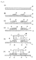
Fig. 2 is a process diagram illustrating surface mounting procedures in a method for surface mounting the electronic component, according to Embodiment 1 of the present invention. -
Fig. 3 is a descriptive diagram of a method for surface mounting an electronic component, according to Embodiment 2 of the present invention. -
Fig. 4 is a process diagram illustrating surface mounting procedures in a method for surface mounting the electronic component, according to Embodiment 3 of the present invention. -
Fig. 5 is a process diagram illustrating surface mounting procedures according to Conventional Example 1. -
Fig. 6 is a schematic sectional view of a substrate with an electronic component mounted thereon, which is obtained by a method for surface mounting according to Conventional Example 2. -
Fig. 7 is a process diagram illustrating surface mounting procedures according to Conventional Example 2. - Hereinafter, embodiments for carrying out this invention will be exemplified and described in detail based on embodiments with reference to the drawings. However, dimensions, materials, shapes, relative positions, and the like described in the embodiments are not purposed for limiting the scope of this invention thereto unless otherwise specifically described so.
- A description will be given of a method for surface mounting an electronic component, and a substrate having an electronic component mounted thereon according to Embodiment 1 of the present invention, with reference to
Figs. 1 and2 . - Referring, in particular, to
Fig. 1 , a substrate having an electronic component produced by a method for surface mounting an electronic component according to Embodiment 1 of the present invention will be described. - A
substrate 100 having an electronic component mounted thereon according to this embodiment includes an insulatingbase material 10 as a substrate member, aconductive circuit 21 formed on a surface of the insulatingbase material 10, andmetal layers 50 provided on a pair ofelectrodes 41 of anelectronic component 40 and fixed while being electrically connected to theconductive circuit 21. Further, thesubstrate 100 is also provided with aresin fixing portion 31 that functions to further reinforce fixing between the insulatingbase material 10 and theelectronic component 40. - Here, a glass epoxy resin is named as a preferred example as a material of the insulating
base material 10. In addition, in this embodiment, various types of electronic components that can be mounted by surface mounting, such as a resistor and a capacitor, are applied as theelectronic component 40. - Referring, in particular, to
Fig. 2 , a method for surface mounting an electronic component according to this embodiment will be described. - A
metal foil 20 is laminated on a surface of the insulating base material 10 (seeFig. 2(A) ). - As a specific example, the
metal foil 20 made of hard aluminum having a thickness of 35 µm is placed on one side of the insulating base material (Garaepoprepreg) 10 made of glass epoxy having a thickness of 50 µm, which are joined together by hot press. Since this bonding method is a publicly known technique, and the detailed description thereof will be omitted. - As a result of this, the insulating
base material 10 including themetal foil 20 laminated on a surface thereof can be obtained. Here, a copper foil having a thickness of 18 µm is named as another specific example of themetal foil 20. - A desired pattern shape (shape of the conductive circuit) of a resist 30 is formed on a surface of the
metal foil 20 by an ink material made of a thermoplastic resin (seeFig. 2(B) ). - As a specific example, a desired pattern shape of the resist 30 (thermoplastic resin layer) is formed on the surface of the
metal foil 20 by a polyolefin thermoplastic adhesive or the like which melts at a temperature of about 150°C. The resist 30 is formed by coating to a thickness of about 2 to 3 µm by a method such as gravure printing. - The
metal foil 20 in an exposed position which is not covered with the resist 30 is removed by etching to thereby form theconductive circuit 21. A surface of thisconductive circuit 21 is covered with the resist 30 serving as a thermoplastic resin layer (seeFig. 2(C) ). - As a specific example, as an etching process, it is preferable to use NaOH (120 g/l) as an etchant at a temperature condition of 50°C. Here, it is also possible to use a polyester plastic resin instead of the polyolefin thermoplastic resin which is used for the resist 30. In this case, FeCl2 of an acid system is used as the etchant during etching.
- In this embodiment, an area of the bonded portion of the
conductive circuit 21 can be made smaller than an area of the bonded portion of theelectrode 41 of theelectronic component 40. For this reason, the area of the bonded portion of theconductive circuit 21 can be made smaller as compared with the conventional method for mounting using a solder material (e.g., in the case of a chip capacitor having a size of 1.0 mm by 0.5 mm, an area about a twice an electrode area is necessary). - In the separate process, a
metal layer 50 serving as a thin layer having a thickness of about 1 µm is formed, by plating or the like, on an entire surface on a side to be joined of theelectrode 41 of the electronic component 40 (seeFig. 2(D) ). Here, a material used to form themetal layer 50 is a material having a shear strength (shearing resistance) smaller than that of a material constituting theconductive circuit 21. In addition, both surfaces of themetal layer 50 are formed to have flat surfaces. - As a specific example, the
metal layer 50 is formed to have a thickness of about 1 µm by a conventional gold plating method using gold having a shear strength of 1600 kg/cm2 on an entire surface on a side to be joined to theconductive circuit 21, and this is applied to each of the pair ofelectrodes 41 of a chip capacitor (electronic component 40) having a size of 1.0 mm by 0.5 mm. - Here, when the
conductive circuit 21 is formed of aluminum, the shear strength is about 2000 to 3000 kg/cm2, and about 3000 kg/cm2 or more when it is formed of copper. Accordingly, in any of the cases, the shear strength of themetal layer 50 is lower than the shear strength of theconductive circuit 21. - In this embodiment, the case where the
metal layer 50 is provided only on a surface of theelectrode 41 on a side to be joined to theconductive circuit 21. However, it is also possible to form themetal layer 50 on an entire exposed surface of theelectrode 41. In this case, it is not necessary to make an arrangement so that plating is not applied to surfaces (upper surface and side surfaces) other than the surface of theelectrode 41 on the side to be joined, so that a process of forming themetal layer 50 can be simplified. - A load generated by ultrasonic vibration vibrating in a direction substantially parallel to a surface of the
metal layer 50 is applied while themetal layer 50 provided on the surface of theelectrode 41 of theelectronic component 40 is pressed against the resist 30 serving as the thermoplastic resin layer (seeFig. 2(E) ). This process is performed while the insulatingbase material 10 having theconductive circuit 21 on which the resist 30 is formed is heated to a temperature of about 60°C. - By applying a load by ultrasonic vibration while a load by pressure is applied, a part of the resist 30 formed of the thermoplastic resin is removed from the surface of the
conductive circuit 21 by mechanical friction caused by the ultrasonic vibration. To state it differently, a part of the resist 30 melts by frictional heat, and the resin that is melted by pressure is pushed away in a direction perpendicular to a direction in which the pressure is exerted and removed from a region between the surface of themetal layer 50 and the surface of theconductive circuit 21. - At the same time, an oxide layer on the surface of the
conductive circuit 21 is also mechanically removed so that the surface of themetal layer 50 on theelectrode 41 makes contact with the surface of theconductive circuit 21. Furthermore, a metal fused portion is formed between these surfaces by the friction caused by the ultrasonic vibration. - Subsequently, by stopping applying the load generated by the ultrasonic vibration, the thermoplastic resin that has been melted by heat is hardened again by cooling. With this arrangement, the
resin fixing portion 31 exerting a function of reinforcing the fixing between the insulatingbase material 10 and theelectronic component 40 is formed (seeFig. 2(F) ). - As a specific example, the load generated by the ultrasonic vibration at a vibration frequency of 63 kHz is applied while the
metal layer 50 provided on theelectrode 41 of the chip capacitor (electronic component 40) is pressed against the resist 30 under the condition of a pressure of 0.2 kg/mm2. - The process of applying the load is performed for about 0.3 seconds. With this arrangement, the chip capacitor is firmly fixed on the insulating
base material 10, and theelectrode 41 of the chip capacitor and theconductive circuit 21 on the insulatingbase material 10 can be electrically connected to each other through themetal layer 50. As described above, since the metal fused portion is formed between themetal layer 50 and theconductive circuit 21, they are firmly fixed together. - Although a case of using gold as one example of a material of the
metal layer 50 is described, the material of themetal layer 50 is not limited to gold. A material having conductivity, and a shear strength (shearing resistance) smaller than that of a material constituting theconductive circuit 21 may serve as the material of themetal layer 50. Accordingly, other than gold, aluminum, zinc, nickel, copper, or an alloy made by arbitrarily combining these, or the like can be used according to the material that constitutes theconductive circuit 21. - Further, as one example of the insulating
base material 10, the material made of glass epoxy having a thickness of 50 µm is described. However, the material and the thickness of the insulatingbase material 10 are not limited to this example. - In this embodiment, since a time required for applying the load generated by the ultrasonic vibration is very short. Therefore, heat caused by the friction is not conducted to the insulating
base material 10. For this reason, it is possible to use a PET film (e.g., thickness of 25 µm) having low heat resistance with a melting point of about 120°C can be used as the insulatingbase material 10. - As described above, according to the method for surface mounting of this embodiment, it is possible to mount the
electronic component 40 on the insulatingbase material 10 without using the solder material. Accordingly, the following effects can be provided. - The method does not provide a problem such as a disconnection of line or short-circuiting caused by insufficient supply or protrusion of the solder material, and therefore the area of the
conductive circuit 21 can be made smaller. There is no need to form a fillet for securing a reliability in solder bonding, and therefore the area of theconductive circuit 21 can be made smaller. The method does not provide a problem of wettability of materials constituting the solder material and theconductive circuit 21, and therefore the cost for material can be reduced because plating on the surface of theconductive circuit 21 can be eliminated, inexpensive aluminum can be employed as a material of theconductive circuit 21, and the like. Heat treatment for melting the solder material is not necessary, and therefore an inexpensive low heat resistant material such as PET (polyethylene terephthalate) can be used as a material for the base material (insulating base material 10) of the printed wiring board. By reducing apparatuses required for heat treatment at a high temperature and energy used therefor, a further reduction in manufacturing cost is possible. Additionally, it is possible to save the impact on the environment by reducing the used energy, or the solder material and the flux material which are required in the conventional method. - Further, cracks, voids, and whiskers resulted from using the solder material are not caused, and a reduction in quality such as uplift of the electronic component is not caused. Moreover, works which are required in the conventional method such as removing of etching resist, coating of resist, plating, supplying solder material, heat treatment, and cleaning of flux material are not necessary, and therefore the processing steps can be drastically reduced. As a result of this, it is possible to reduce the manufacturing cost and improve the productivity.
- As described above, in this embodiment, the
metal layer 50 provided on the surface of theelectronic component 40 is formed of a thin layer (a layer having a flat surface on a side of the conductive circuit 21) made of a material having a shear strength smaller than that of the material constituting theconductive circuit 21. Accordingly, the following effects can be provided. - Specifically, in this embodiment, as a result of employing the foregoing structure as the
metal layer 50, it is possible to prevent theconductive circuit 21 from being broken even if a load is applied by the ultrasonic vibration. This is because the shear strength of theconductive circuit 21 is higher than that of themetal layer 50, and the surface of themetal layer 50 is a flat surface. - In addition, as a result of employing the foregoing structure for the
metal layer 50, a load caused by the shear stress can be suppressed in the bonded portion (referred to as "first bonded portion" for convenient sake) between theelectrode 41 of theelectronic component 40 and themetal layer 50 and in the bonded portion (referred to as "second bonded portion" for convenient sake) between themetal layer 50 and theconductive circuit 21. The reasons are described below. - First, as compared with a case where the thermoplastic resin layer is partially removed from a tip end of the protruding electrode utilizing the ultrasonic vibration, and the protruding electrode and the conductive circuit are joined together, an area of the second bonded portion is wider, and therefore the shear stress can be reduced.
- Second, as compared with a case of the protruding electrode, the thickness (this corresponds to the thickness of the layer of the
metal layer 50 in the case of this embodiment, or a protruding amount in the case of the protruding electrode) can be reduced, and therefore the stress moment caused between the first bonded portion and the second bonded portion can be reduced, and therefore the shear stress in each of the bonded portions can be reduced. - Third, as compared with a case of the protrusion electrode, the
metal layer 50 according to this embodiment has a larger elastic deformation area, the ductility is increased, and therefore it is easy to absorb the shear stress. - As described above, according to this embodiment, breakage of the
conductive circuit 21 is deterred, the load caused by the shear stress exerted on each bonded portion can be suppressed, and therefore it is possible to suppress the occurrence of cracks in the joint interface. - In addition, in the conventional case where the protruding electrode is employed, it is necessary to provide a process of forming a plating mask or the like, whereas, in this embodiment, such a process is not necessary, and therefore it is possible to perform surface mounting the electronic component at a low cost corresponding to about 50% of the cost required in the conventional process.
-
Fig. 3 illustrate Embodiment 2 of the present invention. In this embodiment, a case where particles made of a hard material are dispersed in a thermoplastic resin layer (resist) based on the structure indicated in Embodiment 1. Other structures and working are identical with those of Embodiment 1, and therefore identical constituent portions are identified with identical reference numerals, and the descriptions thereof will be omitted. - As described in Embodiment 1, a material having a shear strength smaller than that of a material constituting the
conductive circuit 21 can be employed as a material of themetal layer 50. For example, it is possible to use tin (Sn) having a shear strength of about 200 kg/cm2. - However, to electrically connect the
metal layer 50 and theconductive circuit 21 together, it is necessary to fuse and remove a part of the thermoplastic resin (resist 30) by themetal layer 50 by applying a load generated by the ultrasonic vibration, and also remove a layer of an oxide on the surface of theconductive circuit 21. - Here, the Mohs hardness of tin is about 1.5 which is lower than the Mohs hardness of aluminum or copper. The Mohs hardness of aluminum is 2.75, and the Mohs harness of copper is 2.5 to 3.0.
- Accordingly, when tin is employed as a material of the
metal layer 50 in the case where copper or aluminum is used as a material of theconductive circuit 21, removing the layer of an oxide on the surface of theconductive circuit 21 by the ultrasonic friction is difficult to progress, and the formation of the metal fused portion between themetal layer 50 and the conductive circuit 21 s difficult to progress. - In this embodiment, a method for forming the metal fused portion in a preferable manner between the
metal layer 50 and theconductive circuit 21 will be described even in the case where a material such as tin having a small Mohs hardness is employed as a material of themetal layer 50. - Specifically, this embodiment adopts, for a resist 30a, a structure in which
particles 30b made of a material having a Mohs hardness that is larger than a Mohs hardness of a material constituting themetallic layer 50 and at the same time larger than a Mohs hardness of a material constituting theconductive circuit 21 are dispersed in a thermoplastic resin layer having a thickness of about 2 µm to 3 µm (seeFig. 3(A) ). - A polyolefin resin is named as a preferred example of the thermoplastic resin. Further, named as a preferred example as the
particles 30b are particles that are made of ceramic such as SiO2, Al2O3, or SiC, and have a substantially spherical shape and a diameter of 0.3 µm or larger and 0.5 µm or smaller. - The method for surface mounting (process) is the same as that of Embodiment 1, and therefore the description thereof will be omitted.
- As described above, in this embodiment, a resist 30a in which the
particles 30b having a large Mohs hardness are dispersed in the thermoplastic resin layer is employed. As a result, in the process of applying the load generated by the ultrasonic vibration in Process 4 which is described in Embodiment 1, what is different from Embodiment 1 is that a frictional force by theparticles 30b is applied to themetal layer 50 and theconductive circuit 21.Fig. 3(B) is a schematic cross sectional view illustrating a state, before themetal layer 50 and theconductive circuit 21 make contact with each other, in which a load generated by the ultrasonic vibration is applied, and a part of the thermoplastic resin melts and is removed. Further,Fig. 3(C) is a schematic cross sectional view of a substrate on which the electronic components is mounted (schematic cross sectional view illustrating a state after the process of applying the load generated by the ultrasonic vibration). As illustrated, and as in the case of Embodiment 1, the thermoplastic resin that has been melted by heat is hardened again by cooling, and aresin fixing portion 31a exerting a function of reinforcing the fixing between the insulatingbase material 10 and theelectronic component 40 is formed. - In Process 4 described in Embodiment 1, when the
metal layer 50 and theconductive circuit 21 make frictional contact with each other by the ultrasonic vibration, if there is a difference in the Mohs hardness between the two, destruction of the surface oxide film of the one having a higher Mohs hardness does not progress, which poses a problem of a difficulty in forming the metal fused portion. However, according to this embodiment, theparticles 30b dispersed in the thermoplastic resin rub against the interface between themetal layer 50 and theconductive circuit 21, and therefore the surface oxides of the both are uniformly destroyed, so that the metal fused portion can be formed in a preferable manner. - As described above, according to this embodiment, even in the case where a material such as tin having a small Mohs hardness is used as the material of the
metal layer 50, the metal fused portion can be formed between themetal layer 50 and theconductive circuit 21 in a preferable manner. -
Fig. 4 illustrates Embodiment 3 of the present invention. In Embodiment 1, the case where the metal layer is provided on the side of the electrode of the electronic component is described, as a process before fixing the electronic component to the insulating base material. In this embodiment, a case where the metal layer is provided on the side of the insulating base material will be described. Other structures and working are identical with those of Embodiment 1, and therefore identical constituent portions are identified with identical reference numerals, and the descriptions thereof will be omitted. - In Embodiment 1, the case where the
metal layer 50 is provided on the surface of theelectrode 41 of theelectronic component 40 is described, as a process before fixing theelectronic component 40 to the insulatingbase material 10. However, a surface on a bonding side of theelectrode 41 to be joined to theconductive circuit 21 has a sufficient area. Therefore, it is not necessary to position theelectronic component 40 with respect to theconductive circuit 21 with a high degree of accuracy in Process 4 in Embodiment 1. - Accordingly, for the purpose of reducing the cost or the like, it is also possible to provide the metal layer on the side of the insulating base material 10 (to be more specific, on the surface of the conductive circuit 21) as a process before the
electronic component 40 is fixed to the insulatingbase material 10. - Referring, in particular, to
Fig. 4 , a method for surface mounting an electronic component according to this embodiment will be described. - As in the case of Embodiment 1, a
metal foil 20 is laminated on a surface of the insulating base material 10 (seeFig. 4(A) ). - As a specific example, the metal foil (copper foil) 20 having a thickness of 18 µm is placed on one side of the insulating base material (Garaepoprepreg) 10 made of glass epoxy having a thickness of 50 µm, which are joined together by hot press. As a result of this, the insulating
base material 10 including themetal foil 20 laminated on a surface thereof can be obtained. - After a desired pattern shape of a resist for plating is formed on a surface of the
metal foil 20, ametal layer 55 is formed through the conventional plating process (electroless plating or electrolytic plating process) on an exposed portion of themetal foil 20 which is not covered with the resist for plating. As in the case of Embodiment 1, a material used to form themetal layer 55 is a material having a shear strength (shearing resistance) smaller than that of a material constituting theconductive circuit 21. In addition, both surfaces of themetal layer 55 are formed to have flat surfaces. As in the case of Embodiment 1, thismetal layer 55 is also formed of a thin layer having a thickness of about 1 µm. Further, as in the case of Example 1, gold, aluminum, zinc, nickel, copper, or an alloy made by arbitrarily combining these, or the like can be used according to the material that constitutes theconductive circuit 21, also as the material of thismetal layer 55. - After the
metal layer 55 is formed, the resist for plating is peeled off from the metal foil 20 (seeFig. 4(B)). Fig. 4 does not illustrate the resist for plaiting. - A desired pattern shape (shape of the conductive circuit) of a resist 35 is formed on a surface of the
metal foil 20 including a portion where themetal layer 55 is provided by an ink material made of a thermoplastic resin (seeFig. 4(C) ). - As a specific example, a desired pattern shape of the resist 35 (thermoplastic resin layer) is formed on the surface of the
metal foil 20 including the portion where themetal layer 55 is provided using a polyolefin thermoplastic adhesive or the like which melts at a temperature of about 150°C. The resist 30 is formed by coating to a thickness of about 2 to 3 µm by a method such as gravure printing. - The
metal foil 20 in an exposed position which is not covered with the resist 35 is removed by etching to thereby form theconductive circuit 21. A surface of thisconductive circuit 21 is covered with the resist 35 serving as a thermoplastic resin layer, and a portion thereof provided with themetal film 55 is covered with the resist 35 in a manner to sandwich the metal layer 55 (seeFig. 4(D) ). - A load generated by ultrasonic vibration vibrating in a direction substantially parallel to a surface of the
electrode 41 is applied while the surface of theelectrode 41 of theelectronic component 40 is pressed against the resist 35 serving as the thermoplastic resin layer (seeFig. 4(E) ). This process is performed while the insulatingbase material 10 having theconductive circuit 21 on which the resist 35 or the like is formed is heated to a temperature of about 60°C. - The mechanism in which the
electrode 41 of theelectronic component 40 and themetal layer 55 are electrically joined together is the same as that in the case of Embodiment 1. - Specifically, by applying a load generated by the ultrasonic vibration while a load by pressure is applied, a part of the resist 35 formed of the thermoplastic resin is removed from the surface of the
metal layer 55 by mechanical friction caused by the ultrasonic vibration. To state it differently, a part of the resist 35 melts by frictional heat, and the resin that is melted by pressure is pushed away in a direction perpendicular to a direction in which the pressure is exerted and removed from a region between the surface of theelectrode 41 of theelectronic component 40 and the surface of themetal layer 55. - At the same time, an oxide layer on the surface of the
electrode 41 is also mechanically removed so that the surface of theelectrode 41 makes contact with the surface of themetal layer 55. Furthermore, a metal fused portion is formed between these surfaces by the friction caused by the ultrasonic vibration. - Subsequently, by stopping applying the load generated by the ultrasonic vibration, the thermoplastic resin that has been melted by heat is hardened again by cooling. With this arrangement, a
resin fixing portion 36 exerting a function of reinforcing the fixing between the insulatingbase material 10 and theelectronic component 40 is formed (seeFig. 4(F) ). - As to Process 5, specific examples of a pressure of pressing the
electronic component 40, a vibration frequency of the ultrasonic vibration, a duration for applying the load are the same as those in the case of Embodiment 1 as described earlier, and therefore the descriptions thereof will be omitted. - As described above, a similar effect as in the case of Embodiment 1 can also be provided in this embodiment. Also, in this embodiment, by dispersing the particles made of a hard material in a thermoplastic resin layer (resist 35) as described in Embodiment 2, it is possible to increase the frictional force while the load generated by the ultrasonic vibration is applied.
- It is preferable to arrange the thicknesses of the metal layers 50 and 55 in each of the embodiments to be 1 µm or more and 3 µm or less. The reason for setting the thicknesses of the metal layers 50 and 55 to 1 µm or more is that an amount to be scraped off by the ultrasonic friction is taken into account. In the case where the thicknesses of the metal layers 50 and 55 are set to a thickness smaller than 1 µm, it is possible that metal serving as the electrode is absent in the interface, and as a result a probability of causing bonding failure is increased. Further, it serves as a factor to raise the cost to make the thicknesses of the metal layers 50 and 55 larger, and a risk of generating cracks inside the metal layer is caused if the thicknesses are too large. Accordingly, it is preferable that the upper limit of the thicknesses of the metal layers 50 and 55 be about 3 µm.
-
DESCRIPTION OF SYMBOLS 10 Insulating base material 20 Metal foil 21 Conductive circuit 30 Resist 30a Resist 30b Particles 31 Resin fixing portion 35 Resist 40 Electronic component 41 Electrode 50 Metal layer 55 Metal layer 100 Substrate
Claims (4)
- A method for surface mounting an electronic component, comprising the steps of:providing, on a substrate member, a conductive circuit, and a thermoplastic resin layer which is formed on a front surface of the conductive circuit;providing a surface of an electrode of an electronic component with a metal layer; andbonding the metal layer of the electronic component and the conductive circuit to each other by melting and partially removing a thermoplastic resin by applying a load generated by ultrasonic vibration that vibrates in a direction substantially parallel to a surface of the metal layer, while pressing the metal layer to the thermoplastic resin layer, and then stopping applying the load generated by the ultrasonic vibration, and hardening the thermoplastic resin thus melted by cooling, whereinthe metal layer is configured by a thin layer made of a material having a shear strength lower than that of a material constituting the conductive circuit.
- The method for surface mounting an electronic component according to claim 1, wherein
particles made of a material having a Mohs hardness larger than that of the material constituting the conductive circuit are dispersed in the thermoplastic resin layer. - A method for surface mounting an electronic component, comprising the steps of:providing, on a substrate member, a conductive circuit, and a metal layer which is formed on a front surface of the conductive circuit;providing a front surface of the metal layer with a thermoplastic resin layer;
andbonding an electrode of an electronic component and the metal layer to each other by melting and partially removing a thermoplastic resin by applying a load generated by ultrasonic vibration that vibrates in a direction substantially parallel to a surface of the electrode, while pressing the surface of the electrode to the thermoplastic resin layer, and then stopping applying the load generated by the ultrasonic vibration, and hardening the thermoplastic resin thus melted by cooling, whereinthe metal layer is configured by a thin layer made of a material having a shear strength lower than that of a material constituting the conductive circuit. - A substrate having an electronic component mounted thereon, wherein
the electronic component is mounted on a substrate member by the method for surface mounting an electronic component according to claim 1, 2, or 3.
Applications Claiming Priority (2)
| Application Number | Priority Date | Filing Date | Title |
|---|---|---|---|
| JP2010199832A JP5644286B2 (en) | 2010-09-07 | 2010-09-07 | Electronic component surface mounting method and electronic component mounted substrate |
| PCT/JP2011/065485 WO2012032840A1 (en) | 2010-09-07 | 2011-07-06 | Method for surface mounting electronic component, and substrate having electronic component mounted thereon |
Publications (2)
| Publication Number | Publication Date |
|---|---|
| EP2615891A1 true EP2615891A1 (en) | 2013-07-17 |
| EP2615891A4 EP2615891A4 (en) | 2016-05-04 |
Family
ID=45810445
Family Applications (1)
| Application Number | Title | Priority Date | Filing Date |
|---|---|---|---|
| EP11823319.6A Withdrawn EP2615891A4 (en) | 2010-09-07 | 2011-07-06 | METHOD FOR SURFACE MOUNTING AN ELECTRONIC COMPONENT, AND SUBSTRATE CARRYING A MOUNTED ELECTRONIC COMPONENT |
Country Status (6)
| Country | Link |
|---|---|
| US (1) | US20130175074A1 (en) |
| EP (1) | EP2615891A4 (en) |
| JP (1) | JP5644286B2 (en) |
| KR (2) | KR20130039328A (en) |
| CN (1) | CN103004294B (en) |
| WO (1) | WO2012032840A1 (en) |
Families Citing this family (6)
| Publication number | Priority date | Publication date | Assignee | Title |
|---|---|---|---|---|
| WO2014115358A1 (en) * | 2013-01-25 | 2014-07-31 | 株式会社村田製作所 | Module and manufacturing method thereof |
| JP6694235B2 (en) * | 2015-01-29 | 2020-05-13 | Tdk株式会社 | Electronic parts |
| CN114980553A (en) * | 2016-03-29 | 2022-08-30 | 积水保力马科技株式会社 | Flexible circuit board and method for manufacturing flexible circuit board |
| KR101932337B1 (en) | 2017-04-12 | 2018-12-26 | 한국과학기술원 | Anisotropic conductive film including polymer layer for suppressing movement of conductive particles and manufacturing method thereof using vertical ultrasonic wave |
| CN111566787A (en) * | 2018-01-17 | 2020-08-21 | 思美定株式会社 | Mounting body |
| JP2022148418A (en) * | 2021-03-24 | 2022-10-06 | 株式会社ワンダーフューチャーコーポレーション | Electronic circuit and manufacturing method for the same |
Family Cites Families (53)
| Publication number | Priority date | Publication date | Assignee | Title |
|---|---|---|---|---|
| JPS629642A (en) * | 1985-07-05 | 1987-01-17 | Matsushita Electric Ind Co Ltd | Manufacture of semiconductor device |
| JPS63169793A (en) * | 1987-01-07 | 1988-07-13 | 株式会社村田製作所 | Structure of fitting chip parts onto printed board |
| WO1990004263A1 (en) * | 1988-10-14 | 1990-04-19 | Matsushita Electric Industrial Co., Ltd. | Image sensor and method of producing the same |
| GB9222460D0 (en) * | 1992-10-26 | 1992-12-09 | Hughes Microelectronics Europa | Radio frequency baggage tag |
| US5821627A (en) * | 1993-03-11 | 1998-10-13 | Kabushiki Kaisha Toshiba | Electronic circuit device |
| US5311405A (en) * | 1993-08-02 | 1994-05-10 | Motorola, Inc. | Method and apparatus for aligning and attaching a surface mount component |
| JP3141692B2 (en) * | 1994-08-11 | 2001-03-05 | 松下電器産業株式会社 | Millimeter wave detector |
| EP0732107A3 (en) * | 1995-03-16 | 1997-05-07 | Toshiba Kk | Screen device for circuit substrate |
| US5629241A (en) * | 1995-07-07 | 1997-05-13 | Hughes Aircraft Company | Microwave/millimeter wave circuit structure with discrete flip-chip mounted elements, and method of fabricating the same |
| US5686318A (en) * | 1995-12-22 | 1997-11-11 | Micron Technology, Inc. | Method of forming a die-to-insert permanent connection |
| US5821456A (en) * | 1996-05-01 | 1998-10-13 | Motorola, Inc. | Microelectronic assembly including a decomposable encapsulant, and method for forming and reworking same |
| US6558979B2 (en) * | 1996-05-21 | 2003-05-06 | Micron Technology, Inc. | Use of palladium in IC manufacturing with conductive polymer bump |
| US20010000157A1 (en) * | 1997-10-16 | 2001-04-05 | Rohm Co., Ltd. | Semiconductor device and method of making the same |
| JP3119230B2 (en) * | 1998-03-03 | 2000-12-18 | 日本電気株式会社 | Resin film and method for connecting electronic components using the same |
| EP1156520A4 (en) * | 1999-01-29 | 2004-08-25 | Matsushita Electric Industrial Co Ltd | METHOD AND DEVICE FOR MOUNTING ELECTRONIC PARTS |
| US6546420B1 (en) * | 1999-03-31 | 2003-04-08 | Cisco Technology, Inc. | Aggregating information about network message flows |
| JP3928682B2 (en) * | 1999-06-22 | 2007-06-13 | オムロン株式会社 | Wiring board bonded body, wiring board bonding method, data carrier manufacturing method, and electronic component module mounting apparatus |
| JP3227444B2 (en) * | 1999-11-10 | 2001-11-12 | ソニーケミカル株式会社 | Flexible wiring board having multilayer structure and method of manufacturing the same |
| JP3451373B2 (en) * | 1999-11-24 | 2003-09-29 | オムロン株式会社 | Manufacturing method of data carrier capable of reading electromagnetic wave |
| JP2001257239A (en) * | 2000-03-13 | 2001-09-21 | Matsushita Electric Ind Co Ltd | Method for manufacturing semiconductor device |
| TW569424B (en) * | 2000-03-17 | 2004-01-01 | Matsushita Electric Industrial Co Ltd | Module with embedded electric elements and the manufacturing method thereof |
| US6512183B2 (en) * | 2000-10-10 | 2003-01-28 | Matsushita Electric Industrial Co., Ltd. | Electronic component mounted member and repair method thereof |
| JP3866058B2 (en) * | 2001-07-05 | 2007-01-10 | シャープ株式会社 | Semiconductor device, wiring board and tape carrier |
| JP3533665B1 (en) * | 2002-12-17 | 2004-05-31 | オムロン株式会社 | A method for manufacturing an electronic component module and a method for manufacturing a data carrier capable of reading electromagnetic waves. |
| US6800946B2 (en) * | 2002-12-23 | 2004-10-05 | Motorola, Inc | Selective underfill for flip chips and flip-chip assemblies |
| JP3584404B2 (en) | 2003-01-17 | 2004-11-04 | オムロン株式会社 | Semiconductor chip mounting method |
| JP2005033053A (en) * | 2003-07-08 | 2005-02-03 | Lintec Corp | Semiconductor device manufacturing method and semiconductor device |
| US20070075436A1 (en) * | 2003-10-06 | 2007-04-05 | Nec Corporation | Electronic device and manufacturing method of the same |
| JP2005203693A (en) | 2004-01-19 | 2005-07-28 | Mitsubishi Electric Corp | Connection sheet and mounting component mounting method |
| JP2005275802A (en) * | 2004-03-24 | 2005-10-06 | Omron Corp | Manufacturing method of radio wave readable data carrier, substrate used in manufacturing method, and electronic component module |
| JP4605155B2 (en) * | 2004-03-29 | 2011-01-05 | 日本電気株式会社 | Semiconductor device and manufacturing method thereof |
| JP4251104B2 (en) * | 2004-03-31 | 2009-04-08 | 株式会社日立製作所 | RFID tag manufacturing method |
| JP4536430B2 (en) * | 2004-06-10 | 2010-09-01 | イビデン株式会社 | Flex rigid wiring board |
| KR100580329B1 (en) * | 2004-06-25 | 2006-05-16 | 삼성전자주식회사 | Bumped wiring film, film package using the same, and manufacturing method thereof |
| JP4146826B2 (en) * | 2004-09-14 | 2008-09-10 | カシオマイクロニクス株式会社 | Wiring substrate and semiconductor device |
| US7312403B2 (en) * | 2004-09-24 | 2007-12-25 | Matsushita Electric Industrial Co., Ltd. | Circuit component mounting device |
| JP2006165517A (en) * | 2004-11-11 | 2006-06-22 | Sharp Corp | Flexible wiring board, semiconductor device and electronic device using the same, and method for manufacturing flexible wiring board |
| JP4618298B2 (en) * | 2005-03-29 | 2011-01-26 | 株式会社村田製作所 | Electronic component mounting structure |
| EP1897119B1 (en) * | 2005-06-13 | 2010-03-17 | Panasonic Corporation | Semiconductor device bonding apparatus and method for bonding semiconductor device using the same |
| CN101263752B (en) * | 2005-09-20 | 2010-06-09 | 株式会社村田制作所 | Method for manufacturing component-incorporated module and component-incorporated module |
| JP5113346B2 (en) * | 2006-05-22 | 2013-01-09 | 日立電線株式会社 | Electronic device substrate and manufacturing method thereof, and electronic device and manufacturing method thereof |
| CN101347052B (en) * | 2006-08-07 | 2012-02-15 | 日本亚比欧尼克斯股份有限公司 | Method and apparatus for connecting printed wiring boards |
| DE102006054085A1 (en) * | 2006-11-16 | 2008-05-29 | Epcos Ag | Component arrangement |
| CN102051141B (en) * | 2007-01-10 | 2014-12-17 | 日立化成株式会社 | Adhesive for connection of circuit member and semiconductor device using the same |
| US7783141B2 (en) * | 2007-04-04 | 2010-08-24 | Ibiden Co., Ltd. | Substrate for mounting IC chip and device for optical communication |
| JP2009009994A (en) * | 2007-06-26 | 2009-01-15 | Shinko Electric Ind Co Ltd | Semiconductor device and manufacturing method thereof |
| EP2193533B1 (en) * | 2007-06-29 | 2011-05-25 | Koninklijke Philips Electronics N.V. | Electrical contact for a cadmium tellurium component |
| JP4962217B2 (en) * | 2007-08-28 | 2012-06-27 | 富士通株式会社 | Printed wiring board and electronic device manufacturing method |
| JP2009105276A (en) * | 2007-10-24 | 2009-05-14 | Omron Corp | Semiconductor chip mounting method and wiring board for semiconductor mounting |
| JP5150518B2 (en) * | 2008-03-25 | 2013-02-20 | パナソニック株式会社 | Semiconductor device, multilayer wiring board, and manufacturing method thereof |
| JP5407667B2 (en) * | 2008-11-05 | 2014-02-05 | 株式会社村田製作所 | Semiconductor device |
| JP5535570B2 (en) * | 2009-10-13 | 2014-07-02 | ルネサスエレクトロニクス株式会社 | Method for manufacturing solid-state imaging device |
| KR20110058061A (en) * | 2009-11-25 | 2011-06-01 | 삼성전기주식회사 | Die Mounting Board and Manufacturing Method Thereof |
-
2010
- 2010-09-07 JP JP2010199832A patent/JP5644286B2/en not_active Expired - Fee Related
-
2011
- 2011-07-06 CN CN201180034819.4A patent/CN103004294B/en not_active Expired - Fee Related
- 2011-07-06 US US13/810,689 patent/US20130175074A1/en not_active Abandoned
- 2011-07-06 KR KR1020137000772A patent/KR20130039328A/en not_active Ceased
- 2011-07-06 WO PCT/JP2011/065485 patent/WO2012032840A1/en not_active Ceased
- 2011-07-06 KR KR1020147025794A patent/KR20140123595A/en not_active Ceased
- 2011-07-06 EP EP11823319.6A patent/EP2615891A4/en not_active Withdrawn
Non-Patent Citations (1)
| Title |
|---|
| See references of WO2012032840A1 * |
Also Published As
| Publication number | Publication date |
|---|---|
| KR20140123595A (en) | 2014-10-22 |
| JP5644286B2 (en) | 2014-12-24 |
| JP2012059816A (en) | 2012-03-22 |
| EP2615891A4 (en) | 2016-05-04 |
| CN103004294B (en) | 2015-04-29 |
| CN103004294A (en) | 2013-03-27 |
| WO2012032840A1 (en) | 2012-03-15 |
| US20130175074A1 (en) | 2013-07-11 |
| KR20130039328A (en) | 2013-04-19 |
Similar Documents
| Publication | Publication Date | Title |
|---|---|---|
| JP4117851B2 (en) | Method and apparatus for connecting printed wiring board | |
| CN1671274B (en) | Flexible substrate with interlayer junction and manufacturing method thereof | |
| EP2615891A1 (en) | Method for surface mounting electronic component, and substrate having electronic component mounted thereon | |
| CN101252093B (en) | Method of manufacturing an electronic component and an electronic device, the electronic component and electronic device | |
| JPWO2008047918A1 (en) | Electronic device package structure and package manufacturing method | |
| JPWO2009107342A1 (en) | Manufacturing method of electronic component module | |
| JP2010082668A (en) | Joining structure and its manufacturing method | |
| JP6719176B2 (en) | Method of joining aluminum members | |
| KR102520768B1 (en) | Method for ultrasonic bonding for circuit device using anisotropic conductive film | |
| JP4755151B2 (en) | Electrical connection device | |
| CN111742623A (en) | Wiring board with metal sheet and method of manufacturing wiring board with metal sheet | |
| JP5003528B2 (en) | Manufacturing method of electronic component module | |
| JP2004127612A (en) | Conductive fine particles, method for interconnecting electrode terminals, and conductive connection structure | |
| JP2000332373A (en) | Electronic component mounted body and method of manufacturing the same | |
| JP4031899B2 (en) | Manufacturing method of film carrier tape for mounting electronic components | |
| EP0851723A1 (en) | Method for mounting electronic parts | |
| JP4043391B2 (en) | Electronic component mounting method and mounting apparatus therefor | |
| JPH04180029A (en) | Connecting structural body for circuit | |
| JP2005175071A (en) | Thin substrate fixing tool | |
| JP2003218526A (en) | Method of connecting wiring layer between first wiring base and second wiring base | |
| JP2003059978A (en) | Method and apparatus for manufacturing film carrier tape for mounting electronic components | |
| JP2003197806A (en) | Wiring board manufacturing method and wiring board | |
| JP2005223229A (en) | Bonding method, semiconductor device manufacturing method using the same, and semiconductor device | |
| JP2000306952A (en) | Wiring board for mounting and method of manufacturing the same | |
| JP2001007504A (en) | Electronic circuit manufacturing method |
Legal Events
| Date | Code | Title | Description |
|---|---|---|---|
| PUAI | Public reference made under article 153(3) epc to a published international application that has entered the european phase |
Free format text: ORIGINAL CODE: 0009012 |
|
| 17P | Request for examination filed |
Effective date: 20121221 |
|
| AK | Designated contracting states |
Kind code of ref document: A1 Designated state(s): AL AT BE BG CH CY CZ DE DK EE ES FI FR GB GR HR HU IE IS IT LI LT LU LV MC MK MT NL NO PL PT RO RS SE SI SK SM TR |
|
| DAX | Request for extension of the european patent (deleted) | ||
| RA4 | Supplementary search report drawn up and despatched (corrected) |
Effective date: 20160404 |
|
| RIC1 | Information provided on ipc code assigned before grant |
Ipc: H01L 21/60 20060101ALI20160329BHEP Ipc: H05K 3/32 20060101AFI20160329BHEP Ipc: H01L 21/607 20060101ALI20160329BHEP |
|
| STAA | Information on the status of an ep patent application or granted ep patent |
Free format text: STATUS: EXAMINATION IS IN PROGRESS |
|
| 17Q | First examination report despatched |
Effective date: 20181122 |
|
| GRAP | Despatch of communication of intention to grant a patent |
Free format text: ORIGINAL CODE: EPIDOSNIGR1 |
|
| STAA | Information on the status of an ep patent application or granted ep patent |
Free format text: STATUS: GRANT OF PATENT IS INTENDED |
|
| INTG | Intention to grant announced |
Effective date: 20210401 |
|
| STAA | Information on the status of an ep patent application or granted ep patent |
Free format text: STATUS: THE APPLICATION IS DEEMED TO BE WITHDRAWN |
|
| 18D | Application deemed to be withdrawn |
Effective date: 20210812 |