JP3584404B2 - Semiconductor chip mounting method - Google Patents
Semiconductor chip mounting method Download PDFInfo
- Publication number
- JP3584404B2 JP3584404B2 JP2003009971A JP2003009971A JP3584404B2 JP 3584404 B2 JP3584404 B2 JP 3584404B2 JP 2003009971 A JP2003009971 A JP 2003009971A JP 2003009971 A JP2003009971 A JP 2003009971A JP 3584404 B2 JP3584404 B2 JP 3584404B2
- Authority
- JP
- Japan
- Prior art keywords
- thermoplastic resin
- bump
- electrode region
- wiring board
- wiring pattern
- Prior art date
- Legal status (The legal status is an assumption and is not a legal conclusion. Google has not performed a legal analysis and makes no representation as to the accuracy of the status listed.)
- Expired - Lifetime
Links
Images


Classifications
-
- H—ELECTRICITY
- H01—ELECTRIC ELEMENTS
- H01L—SEMICONDUCTOR DEVICES NOT COVERED BY CLASS H10
- H01L2224/00—Indexing scheme for arrangements for connecting or disconnecting semiconductor or solid-state bodies and methods related thereto as covered by H01L24/00
- H01L2224/01—Means for bonding being attached to, or being formed on, the surface to be connected, e.g. chip-to-package, die-attach, "first-level" interconnects; Manufacturing methods related thereto
- H01L2224/10—Bump connectors; Manufacturing methods related thereto
- H01L2224/15—Structure, shape, material or disposition of the bump connectors after the connecting process
- H01L2224/16—Structure, shape, material or disposition of the bump connectors after the connecting process of an individual bump connector
-
- H—ELECTRICITY
- H01—ELECTRIC ELEMENTS
- H01L—SEMICONDUCTOR DEVICES NOT COVERED BY CLASS H10
- H01L2924/00—Indexing scheme for arrangements or methods for connecting or disconnecting semiconductor or solid-state bodies as covered by H01L24/00
- H01L2924/01—Chemical elements
- H01L2924/01005—Boron [B]
-
- H—ELECTRICITY
- H01—ELECTRIC ELEMENTS
- H01L—SEMICONDUCTOR DEVICES NOT COVERED BY CLASS H10
- H01L2924/00—Indexing scheme for arrangements or methods for connecting or disconnecting semiconductor or solid-state bodies as covered by H01L24/00
- H01L2924/01—Chemical elements
- H01L2924/01013—Aluminum [Al]
Description
【0001】
【発明の属する技術分野】
本発明は、航空タグ、物流管理用ラベル、無人改札用パス等として機能する電磁波読み取り可能なデータキャリアの製造等に好適な半導体チップの実装方法に係り、特に、配線基板上に半導体ベアチップをフリップチップ接続方式で低コストに実装可能とした半導体チップの実装方法に関するものである。
【0002】
【従来の技術】
この種の電磁波読み取り可能なデータキャリアとしては、例えば、特開平6−243358号公報に記載された航空タグが知られている。この航空タグは、近い将来、空港における顧客荷物の管理等に使い捨て方式で使用されることが予測され、その際には、例えば世界的規模の航空会社の場合、その1社だけでも月産850万枚と言った膨大の需要が見込まれる。そのため、この種の航空タグに関しては、超低コストな大量生産技術の確立が望まれている。
【0003】
同公報に記載された航空タグは、長方形状を有するPETフィルム製基体の片面に、アンテナコイルとなる渦巻状導体パターンと、送受信回路やメモリ等となるIC部品を搭載して構成されている。
【0004】
アンテナコイルとなる渦巻状導体パターンを保持する航空タグ本体は、PETフィルムの片面に被着された銅箔やアルミ箔をエッチング処理にて選択腐食させることで形成することができる。そのため、公知のフォトリソ技術によるレジスト形成工程、それに続く湿式エッチング工程等により、RTR(Roll ToRoll)による連続生産ラインを容易に実現することができる。一方、航空タグ本体に搭載されるべき送受信回路やメモリ等となる回路部品は半導体集積技術を用いて1チップ化されている。
【0005】
本出願人は、先に、上述の送受信回路やメモリ等を構成する半導体ベアチップを、フィルム状の絶縁性小片(一種の配線基板)に予め実装することでモジュール化を行い、この電子部品モジュールを航空タグ本体を構成するPETフィルム上に接着することで、航空タグの生産性を向上させることを提案している。
【0006】
ところで、航空タグに接着される上述の電子部品モジュールのように、高度の薄型化を要求される電子部品搭載シートにおいては、配線基板上にベアの半導体チップを直接実装するフリップチップ接続方式に関する提案が盛んになされている。
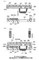
【0007】
フリップチップ接続方式の一例(以下、第1従来方式と言う)が図14に示されている。この第1従来方式にあっては、半導体チップaの底面電極(図示せず)にあらかじめ接続用の突起状端子(以下、バンプと言う)bを形成しておき、このバンプbと配線基板c上の配線パターンの電極領域dとを位置合わせした後、両者間をハンダ、導電性ペースト等の接合材eにより接続するようにしている。
【0008】
この第1従来方式にあっては、(1)バンプbと配線パターンの電極領域dとを接続するための接合材eの供給、硬化等の工程が複雑であること、(2)バンプ接続部分の耐湿信頼性や半導体の搭載強度を得るため、チップaと基板cとの間にアンダーフィルと呼ばれる絶縁樹脂fを充填してバンプ接続部分を封止する必要があること、(3)アンダーフィルとなる絶縁樹脂fを充填硬化させる工程が必要となること、等のために製造コストが高くなると言った問題が指摘されている。
【0009】
フリップチップ接続方式の他の一例(以下、第2従来方式と言う)が図15に示されている。この第2従来方式は第1従来方式の問題点を解決するものであり、特許第2,586,154号公報で提案されているような、異方導電シートを用いて配線基板上に半導体ベアチップを実装するものである。
【0010】
この第2従来方式にあっては、熱可塑性や熱硬化性の樹脂中に導電性の微粒子を分散させた異方導電シートgを半導体ベアチップaと配線基板cとの間に介在させ、熱圧着によって樹脂を流動させ、バンプbと配線パターンの電極領域dとの間に挟まれた導電性の微粒子hによって厚さ方向の電気的接続を得るようにしている。
【0011】
この方法では、半導体を配線基板上に実装する際の配線パターンとの位置合わせが比較的ラフに行える上に、樹脂硬化時間が10〜20秒と短く、アンダーフィル等の封止材を用いる必要がなく、低製造コスト化が狙えると言った効果がある。その反面、(1)異方導電シートgは比較的高価であること、(2)その硬化には200℃以上という高い温度が必要なため、耐熱性のない基板には用いることができないこと、(3)比較的短時間ではあるものの、樹脂材の硬化には10〜20秒を要し、さらなる工程の簡略化、高速化というのは困難であること、(4)バンプと基板パターン間の電気的接続は、樹脂材内に分散された導電微粒子の接触により行うため、接続の信頼性に乏しいこと、等の問題がなおも指摘されている。
【0012】
【発明が解決しようとする課題】
本発明は、従来のフリップチップ接続方式における上述の問題点に着目してなされたものであり、その目的とするところは、配線基板上に半導体チップを迅速に、電気的にも機械的にも確実に、さらに低コストに、実装可能なフリップチップ接続方式による半導体チップの実装方法を提供することにある。
【0013】
また、この発明の他の目的とするところは、上記の実装方法に好適なフリップチップ接続用配線基板を提供することにある。
【0014】
また、この発明の他の目的とするところは、上記の配線基板を簡単かつ低コストに製造可能なフリップチップ接続用配線基板の製造方法を提供することにある。
【0015】
さらに、この発明の他の目的とするところは、航空タグ、物流管理用ラベル、無人改札用パス等として機能する電磁波読み取り可能なデータキャリアを低コストに大量生産することが可能な電磁波読み取り可能なデータキャリアの製造方法を提供することにある。
【0016】
本発明のさらに他の目的並びに効果については、実施の形態の記載等を参照することにより、当業者であれば容易に理解されるであろう。
【0017】
【課題を解決するための手段】
この発明の半導体チップの実装方法は、配線パターン上の電極領域を覆う熱可塑性樹脂被膜を加熱溶融させた状態において、その溶融状態にある熱可塑性樹脂被膜の上に半導体ベアチップのバンプを超音波を付与しつつ押し付けることにより、溶融した熱可塑性樹脂被膜を押し退けてバンプと電極領域とを接触させる工程と、
前記バンプと電極領域とが接触した状態において、超音波を継続的に付与することにより、バンプと電極領域とを超音波接合させる工程と、
前記溶融した熱可塑性樹脂を冷却固化させて、半導体ベアチップ本体を配線基板上に接着させる工程と、
を具備する。
【0018】
ここで、『配線パターン上の電極領域を覆う熱可塑性樹脂被膜を加熱溶融させた状態において、』とあることから明らかなように、この発明で使用される配線基板の配線パターン上の電極領域には、予め熱可塑性樹脂の被膜が形成されている。この被膜は、配線パターンの電極領域のみを覆うものであってもよく、また配線パターン表面の全面を覆うものであってもよい。
【0019】
また、ここで『配線パターン上の電極領域』とは、電子部品の端子等が接続される予定位置を含む配線パターン上の一定小領域を意味する。この電極領域には配線パターン上の一般にはランド等と称される部分が含まれるであろう。
【0020】
また、『加熱溶融』とあるのは、熱可塑性樹脂被膜が加熱されて溶融している状態と加熱されてある程度まで軟化している状態との双方を含む概念を意味している。さらに、ここで言う『熱可塑性樹脂』は、接着剤としての良好な特性を有するものであることが好ましい。
【0021】
そして、このような構成によれば、(1)バンプと電極領域との接合は超音波による拡散接合であるため、確実な電気的導通が図れること、(2)接合部が樹脂封止されるため、耐湿性が良好となることと、(3)半導体チップと配線基板とが熱可塑性樹脂の硬化の際に接着されるため、引っ張り等に対する機械的な実装強度が高いこと、(4)電気的導通と機械的結合とを短時間で同時になし得ること、(5)特別な封止乃至接着工程、並びに、接着材料が不要なため製造コストが低いこと、(6)基板表面が露出している部分については熱可塑性樹脂被膜は存在しないから、加熱時に基板表面が必要以上にべた付くことがないこと、等の作用効果が得られる。
【0022】
また、この発明のフリップチップ接続用配線基板は、配線パターンの表面がその全面に亘って熱可塑性樹脂被膜により覆われている。
【0023】
このような構成によれば、上述の実装方法に使用した場合、配線パターンの表面がその全面に亘って熱可塑性樹脂被膜により覆われているので、耐湿性の良好な封止構造並びに引っ張り強度の高い接着構造が得られる。
【0024】
また、この発明のフリップチップ接続用配線基板の製造方法は、配線パターンをエッチング処理にて形成する際に使用されるエッチングマスク材として熱可塑性樹脂を使用する。
【0025】
このような構成によれば、配線パターンの形成のためのエッチング処理に使用されたエッチングマスク材がそのまま導体パターン表面の全面を覆う熱可塑性樹脂被膜となるため、別途被膜形成工程が不要で手間が掛からず、低コストに製造できる。
【0026】
また、この発明の電磁波読み取り可能なデータキャリアの製造方法は、フィルム状、シート状、乃至薄板状の絶縁性基体にアンテナコイルを構成する渦巻状導体パターンを保持させてなるデータキャリア本体と、フィルム状、シート状、又は薄板状配線基板の配線パターン上に送受信回路やメモリ等を構成する半導体ベアチップを実装してなる電子部品モジュールとを一体化してなる電磁波読み取り可能なデータキャリアの製造方法である。
【0027】
このデータキャリアの製造方法において、主たる特徴的な事項は、前記フィルム状、シート状、又は薄板状配線基板の配線パターン上に半導体ベアチップを実装してなる電子部品モジュールを製造する工程にある。
【0028】
すなわち、この電子部品モジュールを製造する工程には、前記配線パターン上の電極領域を覆う熱可塑性樹脂被膜を加熱溶融させた状態において、その溶融状態にある熱可塑性樹脂被膜の上に半導体ベアチップのバンプを超音波を付与しつつ押し付けることにより、溶融した熱可塑性樹脂被膜を押し退けてバンプと電極領域とを接触させる工程と、前記バンプと電極領域とが接触した状態において、超音波を継続的に付与することにより、バンプと電極領域とを超音波接合させる工程と、前記溶融した熱可塑性樹脂を冷却固化させて、半導体ベアチップ本体を配線基板上に接着させる工程と、が含まれる。
【0029】
そして、このような構成によれば、前述した(1)バンプと電極領域との接合は超音波による拡散接合であるため、確実な電気的導通が図れること、(2)接合部が樹脂封止されるため、耐湿性が良好となることと、(3)半導体チップと配線基板とが熱可塑性樹脂の硬化の際に接着されるため、引っ張り等に対する機械的な実装強度が高いこと、(4)電気的導通と機械的結合とを短時間で同時になし得ること、(5)特別な封止乃至接着工程乃至材料が不要なため製造コストが低いこと、(6)基板表面が露出している部分については熱可塑性樹脂被膜は存在しないから、加熱時に基板表面が必要以上にべた付くことがないこと、等の作用効果を通じて、航空タグ、物流管理用ラベル、無人改札用パス等として機能する電磁波読み取り可能なデータキャリアを低コストに大量生産することが可能となる。
【0030】
また、この発明の電子部品モジュールの製造工程に使用される配線基板は、配線パターンの表面がその全面に亘って熱可塑性樹脂被膜により覆われている。
【0031】
このような構成によれば、上述の電子部品モジュールを製造する工程に使用した場合、配線パターンの表面がその全面に亘って熱可塑性樹脂被膜により覆われているので、耐湿性の良好な封止構造並びに引っ張り強度の高い接着構造が得られる。
【0032】
また、この発明の配線基板の製造方法は、配線パターンをエッチング処理にて形成する際に使用されるエッチングマスク材として熱可塑性樹脂を使用する。
【0033】
このような構成によれば、配線パターンの形成のためのエッチング処理に使用されたエッチングマスク材がそのまま導体パターン表面の全面を覆う熱可塑性樹脂被膜となるため、別途被膜形成工程が不要で手間が掛からず、低コストに製造できる。
【0034】
また、この発明の電磁波読み取り可能なデータキャリアの製造方法は、フィルム状樹脂製基体にアンテナコイルを構成する金属箔パターンを保持させてなるデータキャリア本体と、フィルム状樹脂製基体表面のアルミ箔配線パターンに送受信回路やメモリ等を構成する半導体ベアチップを実装してなる電子部品モジュールとを一体化して構成される電磁波読み取り可能なデータキャリアの製造方法である。
【0035】
この電磁波読み取り可能なデータキャリアの製造方法において、主たる特徴的な事項は、前記フィルム状樹脂製基体表面のアルミ箔配線パターン上に半導体ベアチップを実装してなる電子部品モジュールを製造する工程にある。
【0036】
すなわち、この電子部品モジュールを製造する工程には、前記アルミ箔配線パターン上の電極領域を覆う熱可塑性樹脂被膜を加熱溶融させた状態において、その溶融状態にある熱可塑性樹脂被膜の上に半導体ベアチップのバンプを超音波を付与しつつ押し付けることにより、溶融した熱可塑性樹脂被膜を押し退けてバンプと電極領域とを接触させる工程と、前記バンプと電極領域とが接触した状態において、超音波を継続的に付与することにより、バンプと電極領域とを超音波接合させる工程と、前記溶融した熱可塑性樹脂を冷却固化させて、半導体ベアチップ本体を配線基板上に接着させる工程と、が含まれる。
【0037】
また、この発明の配線基板は、アルミ箔配線パターンの表面がその全面に亘って熱可塑性樹脂被膜により覆われている。
【0038】
また、この発明の配線基板の製造方法は、アルミ箔配線パターンをエッチング処理にて形成する際に使用されるエッチングマスク材として熱可塑性樹脂を使用する。
【0039】
本発明の好ましい実施の形態では、熱可塑性樹脂としては、ポリオレフィン系樹脂又はポリエステル系樹脂が使用される。
【0040】
このような樹脂を使用することにより、エッチングマスクとしての良好な耐薬品性、並びに、半導体チップ側の金属バンプと配線パターン側の金属電極領域との間の良好な接合強度が得られると言う作用効果が期待される。すなわち、ポリオレフィン系樹脂はNaOH等のアルカリ性エッチング液に、又ポリエステル系樹脂はFeCl2等の酸性エッチング液に対して良好な耐性を呈する。しかも、それらの樹脂は、接着性にも優れる。
【0041】
【発明の実施の形態】
以下に、この発明に係る半導体チップの実装方法の好適な実施の一形態を添付図面に従って詳細に説明する。
【0042】
先に述べたように、本発明の半導体チップの実装方法は、配線パターン上の電極領域を覆う熱可塑性樹脂被膜を加熱溶融させた状態において、その溶融状態にある熱可塑性樹脂被膜の上に半導体ベアチップのバンプを超音波を付与しつつ押し付けることにより、溶融した熱可塑性樹脂被膜を押し退けてバンプと電極領域とを接触させる工程と、前記バンプと電極領域とが接触した状態において、超音波を継続的に付与することにより、バンプと電極領域とを超音波接合させる工程と、前記溶融した熱可塑性樹脂を冷却固化させて、半導体ベアチップ本体を配線基板上に接着させる工程と、を具備するものである。
【0043】
斯かる実装方法を含む一連の工程の概略が図1の工程図に示されている。この一連の工程には、金属箔積層材製造工程(A)、エッチングマスク印刷工程(B)、配線パターン形成のためのエッチング工程(C)、超音波実装工程(D)と、接着工程(E)とが含まれている。以下、それらの工程の詳細を順に説明する。
【0044】
[金属箔積層材製造工程(A)]
この工程では、フィルム状配線基板の原材をなすAl−PET積層材1を製造する。このAl−PET積層材1は、例えば、25μm厚のPETフィルム2の片面(図では上面)に、ウレタン系接着剤を介して35μm厚の硬質アルミ箔3を重ね、これを150℃、圧力5kg/cm2の条件で熱ラミネートを経て積層接着させる工程を経て製造される。
【0045】
[エッチングマスク印刷工程(B)]
この工程では、Al−PET積層材1の硬質アルミ箔3の表面に所要配線パターン形状のエッチングレジストパターン4を形成する。このレジストパターン4の形成は、例えば、150℃程度の温度で溶融するポリオレフィン系の熱可塑性樹脂製接着剤を、グラビア印刷等の方法によって硬質アルミ箔3の表面に厚さ4〜6μm程度塗布することによって行われる。この塗布厚は、搭載されるベアチップのバンプサイズ乃至形状に応じて調整することが好ましい。
【0046】
[エッチング工程(C)]
この工程では、エッチングレジストパターン4から露出するアルミ箔部分5を従来公知のエッチング処理で除去することにより、硬質アルミ箔3からなる配線パターン6を形成する。この配線パターン6の形成は、エッチングレジストパターン4から露出するアルミ箔部分5を、例えば、エッチング液であるNaOH(120g/l)に温度50℃の条件にて晒すことによって行われる。このエッチング工程で得られた配線基板7の表面には、硬質アルミ箔3からなる配線パターン6が出現される。また、この配線パターン6の表面は、その全面に亘ってエッチングレジストパターン(エッチングマスク)4として使用したポリオレフィン系の熱可塑性樹脂製接着剤により覆われている。換言すれば、この配線パターン6の少なくとも電極領域(後述する半導体ベアチップのバンプとの接続予定領域)の表面は熱可塑性樹脂被膜4aにより覆われている。
【0047】
[超音波実装工程(D)]
この工程では、超音波を付与しつつ、半導体ベアチップ8を配線基板7上に実装する。この工程は、配線パターン6上の電極領域10を覆う熱可塑性樹脂被膜4aを加熱溶融させた状態において、その溶融状態にある熱可塑性樹脂被膜4aの上に半導体ベアチップ8のバンプ9を超音波を付与しつつ押し付けることにより、溶融した熱可塑性樹脂被膜4aを押し退けてバンプ9と電極領域10とを接触させる工程(第1工程)と、バンプ9と電極領域10とが接触した状態において、超音波を継続的に付与することにより、バンプ9と電極領域10とを超音波接合させる工程(第2工程)と、を含んでいる。
【0048】
すなわち、半導体ベアチップ8は厚さ150μmであって、その底面から接続用の金属端子であるバンプ9を突出させた、いわゆる表面実装型部品として構成されている。第1の工程では、このバンプ(例えば金より成る)9は、超音波振動を付加した状態で、150℃の加熱により溶融した熱可塑性樹脂被膜4aに押し当てられる。すると、溶融した熱可塑性樹脂被膜4aは、バンプ9の超音波振動によりバンプ9の先端位置より押し退けられて除去され、さらにアルミ箔配線パターン6表面上の酸化物層等も振動により機械的に除去される。その結果、バンプ9と電極領域10とが接触させられる。第2の工程では、その後、さらに振動による摩擦熱によりバンプ9と配線パターン6の電極領域10とが加熱され、金原子がアルミ箔内に拡散した金属融着部が形成されて両者の超音波接合が完了する。
【0049】
以上の第1並びに第2の工程は、半導体ベアチップ8を所定位置に配置した後、例えば、負荷圧力0.2kg/mm2下で、振動数63KHzの超音波振動を数秒程度加えることにより完了される。
【0050】
この超音波実装工程のより詳細が図2の工程図に示されている。同図(a)に示される位置決め工程では、それぞれ真空吸着機能を有する超音波ホーン11とヒータテーブル兼用アンビル12とを上下に対向配置した状態において、超音波ホーン11には矢印11aに示されるようにベアチップ8を吸着保持させ、またヒータテーブル兼用アンビル12には矢印12aに示されるように配線基板7を吸着保持させる。この状態において、超音波ホーン11とヒータテーブル兼用アンビル12とを水平方向へと相対移動させつつ、ベアチップ8側のバンプ9と配線基板7側の配線パターン6の電極領域10との位置決めを行い、同時にヒータテーブル兼用アンビル12によって配線基板7を150°Cに加熱する。
【0051】
同図(b)に示される熱可塑性樹脂接着剤の除去工程では、超音波ホーン11とヒータテーブル兼用アンビル12とによって、矢印vに示されるように、超音波振動(63.5KHz、2W)を付与しつつ、矢印Pに示されるように、負荷圧力(0.1〜0.3Kgf)により、ベアチップ8のバンプ9を加熱溶融状態にある熱可塑性樹脂接着剤(熱可塑性樹脂被膜)4aに押し当てることにより、溶融した熱可塑性樹脂被膜4aを押し退けてバンプ9と電極領域10とを接触させる。
【0052】
同図(c)に示される超音波接合工程では、さらに超音波振動vを継続的に付与することにより、金属間の拡散接合を進行させて、バンプ9と電極領域10とを超音波接合させる。
【0053】
再び、図1に戻って、説明を続ける。
[接着工程(E)]
この工程では、配線基板に付与された150℃の加熱を除去することにより、溶融した熱可塑性樹脂被膜4aを自然冷却又は強制冷却により再硬化させて、半導体ベアチップ8本体と配線パターン6との間を接着させる。すなわち、半導体ベアチップ8の底面と配線基板7との間に満たされた溶融状態にある熱可塑性樹脂被膜4aが冷却固化されて、半導体ベアチップ8と配線基板7とが強固に接着固定されるのである。
【0054】
以上の工程(A)〜(E)を経て完成された実装構造が図3に示されている。同図に示されるように、この実装構造によれば、(1)バンプ9と電極領域10との接合は超音波による拡散接合であるため、確実な電気的導通が図れること、(2)バンプ9と電極領域10との接合部が樹脂封止されるため、耐湿性が良好となること、(3)半導体チップ8と配線基板7とが熱可塑性樹脂被膜4aの硬化の際に接着されるため、引っ張り等に対する機械的な実装強度が高いこと、(4)電気的導通と機械的結合とを短時間で同時になし得ること、(5)特別な封止乃至接着工程、並びに、接着材料が不要なため製造コストが格段に低いこと、(6)基板表面が露出している部分については熱可塑性樹脂被膜は存在しないから、加熱時に基板表面が必要以上にべた付くことがないこと、等の作用効果が得られる。
【0055】
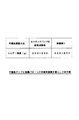
本実施形態の樹脂被膜を用いた実装方法の場合における半導体ベアチップ8と配線パターン6との間の接合強度を、超音波接合のみを用いた場合におけるそれと比較して図4に示す。同図から明らかなように、本発明実装方法の場合には、超音波接合のみの場合に比較して、2〜3倍のもの強力な接合強度が得られた。これは、半導体チップ8と配線基板7とが熱可塑性樹脂被膜4aの硬化の際に接着されるためであることは、言うまでもない。
【0056】
尚、上記の実施形態では、積層材1を構成する樹脂基材としてPETフィルム2を使用したが、PETフィルムの代わりにポリイミドフィルム等を使用することもできる。
【0057】
また、エッチングレジストパターン4の材質としては、ポリオレフィン系樹脂の代わりにポリエステル系の熱可塑性樹脂を用いることもできる。但し、その場合には、エッチング液としては、酸系のFeCl2を用いることとなる。
【0058】
また、図1(C)に示される配線基板7は、配線パターン6の表面がその全面に亘って熱可塑性樹脂被膜4aにより覆われているものであって、フリップチップ接続用配線基板として一般化することができる。
【0059】
そして、このような構成によれば、上述の実装方法に使用した場合、配線パターン6の表面がその全面に亘って熱可塑性樹脂被膜4aにより覆われているので、耐湿性の良好な封止構造並びに引っ張り強度の高い接着構造が得られる。すなわち、配線パターン6上の電極領域10付近に位置する熱可塑性樹脂被膜4aは主として超音波接合部の封止作用に寄与する一方、電極領域以外の部分に位置する熱可塑性樹脂被膜4aは半導体チップ8本体と配線基板7との接着作用に寄与する。
【0060】
また、図1(B),(C)に示される配線基板の製造方法は、換言すれば、配線パターンをエッチング処理にて形成する際に使用されるエッチングマスク材として熱可塑性樹脂を使用するものであって、フリップチップ接続用配線基板の製造方法として一般化することができる。
【0061】
そして、このような構成によれば、配線パターンの形成のためのエッチング処理に使用されたエッチングマスク材がそのまま導体パターン表面の全面を覆う熱可塑性樹脂被膜となるため、別途被膜形成工程が不要で手間が掛からず、低コストに製造できる。
【0062】
最後に、この実施形態にかかる半導体チップの実装方法の作用効果をまとめて記述する。すなわち、以上の実装方法によれば、
(1)配線パターンの形成工程において、エッチング加工で用いた絶縁性レジストを別工程で剥離する必要がなく、低コスト化できる。
【0063】
(2)さらに、熱可塑性樹脂からなる絶縁性レジストが半導体チップの直下で接着剤として働き、超音波による半導体の実装強度を補強できる。
【0064】
(3)また、バンプ周辺を樹脂材により封止でき、バンプ接続部の耐湿信頼性を向上できる。
【0065】
(4)従来方法で必要としていた、上記目的をもった樹脂材が不要であり、材料コストの低下が図れる。
【0066】
(5)超音波振動によるバンプ、配線パターン間の金属の拡散接合により、確実な端子間接続が得られる。
【0067】
(6)超音波接合、熱可塑性樹脂の溶融、硬化は1〜2秒以内で実行でき、製造時間の短縮が図れる。
【0068】
次に、図5〜図10を参照しつつ、本発明にかかるデータキャリアの製造方法の一実施形態について説明する。なお、このデータキャリアは、航空タグ、物流管理用ラベル、無人改札用パス等として機能する電磁波読み取り可能なものである。そして、このデータキャリアは、フィルム状樹脂製基体にアンテナコイルを構成する金属箔パターンを保持させてなるデータキャリア本体と、フィルム状樹脂製基体表面のアルミ箔配線パターンに送受信回路やメモリ等を構成する半導体ベアチップを実装してなる電子部品モジュールとを一体化して構成される。
【0069】
データキャリアの実施形態の一例が図5に示されている。同図に示されるように、このデータキャリアDCは、25μm厚のPET(ポリエチレンテレフタレート)製基体101の片面に、10μm厚の銅箔製渦巻き状導体パターン(アンテナコイルに相当)102を保持させてなるデータキャリア本体100と、70μm厚のガラスエポキシ製小片201にベアチップIC202を図では下面側に実装してなる電子部品モジュール200とを有する。そして、電子部品モジュール200は、その小片201が、渦巻状導体パターン102を構成する周回導体束102aを跨ぐ(換言すれば交差する)ようにしてデータキャリア本体100上に搭載され、かつ渦巻状導体パターン102との電気的接続は、渦巻状導体パターン102の内周側端子パッド103と外周側端子パッド104とにおいて行われる。
【0070】
電子部品モジュール200の実装構造の一例が図6の拡大断面図に示されている。図5並びに図6に示されるデータキャリア本体100並びに電子部品モジュール200の製造方法は、以下に順次詳細に説明される。
【0071】
アンテナコイルを構成する渦巻状導体パターン102の製造工程の一例が図7に示されている。同図を参照して、PETフィルム製基体101の片面にアンテナコイルとなる渦巻状導体パターン102を形成する際の工程を説明する。
【0072】
(工程A)
まず、最初に、Cu−PET積層基材301を用意する。一例として25μm厚のPETフィルム302の片面に、ウレタン系接着剤を介して10μm厚の銅箔303を重ね、これを150℃、圧力5kg/cm2の条件で熱ラミネートを経て積層接着させる。これにより、PETフィルム302の表面に銅箔303が接着されたCu−PET積層材301が完成する。
【0073】
(工程B)
次に、Cu−PET積層材301の銅箔303の表面上に渦巻形状のエッチングレジストパターン304を形成する。すなわち、コイルの特性として必要なL値、Q値を得るターン数、線幅、ピッチ、内外周をもつ渦巻形状に、例えばオフセット印刷法を用いて絶縁性のエッチングレジストインクを銅箔303上に印刷する。このときのレジストインクとしては、熱又は活性エネルギー線で硬化するタイプのものを使用する。活性エネルギー線としては紫外線または電子線を使用し、紫外線を用いる場合にはレジストインクに光重合剤を入れて使用する。
【0074】
(工程C)
次に、Cu−PET積層材301の銅箔303の表面上における、電子部品モジュール200の電極との電気的導通接続を行う位置に、導電性インクで必要電極形状の導電性エッチングレジストパターン305a,305b(図5の103,104)を形成する。このレジストパターン305a,305bの形成は前記工程と同様のオフセット印刷にて行い、レジストインクとしては、120℃、20分程度の熱処理で硬化する熱硬化性導電接着剤を用いる。尚、この工程に於ける導電性インクの印刷は、一般的に実施されるスクリーン印刷法を用いてもよく、またインク材として、例えばAg粒子と熱可塑性接着剤の混合物に光重合剤を入れたもの、あるいはハンダペースト等を用いてもよい。
【0075】
(工程D)
次に、エッチングレジストパターン304,305a,305bから露出する銅箔部分306を従来公知のエッチングを行うことにより除去し、アンテナコイルとなる渦巻状導体パターン(図5における102)を形成する。このエッチング処理に際しては、エッチング液としてFeCl2(120g/l)を50℃の条件にて使用し銅箔303を除去する。この後、一般的には前記工程Bに於いて形成したエッチングレジストを除去しないと、電子部品を回路上、すなわちアンテナコイルを構成する渦巻状パターン上に実装することはできないが、本発明においては先の工程Cで説明したように導電性のレジストパターン305a,305bがあり、この位置に電子部品を実装することによりエッチングレジストを除去する必要がない。すなわち、本発明によりエッチングレジストの剥離工程を省くことができ、さらに絶縁性インクで形成したエッチングレジスト304が銅箔製回路パターン表面の絶縁性保護層としても機能するという効果もある。
【0076】
(工程E)
最後に、本実施形態に於いては後述する電子部品モジュールの凸部(ポッティング部411)が挿入可能な透孔307をプレス加工する。以上によりPETフィルム製基体302(101)の片面にアンテナコイルとなる渦巻状導体パターン308(102)が保持されたデータキャリア本体100が完成する。
【0077】
次に、電子部品モジュール200の作成工程の一例が図8に示されている。なお、図8に示される内容は、最終工程でベアチップ408をポッティング411で樹脂封止すること、並びに、データキャリア本体100との接続用電極部分に導電性レジスト412を配置することを除き、先に図1を参照して説明した内容と同一である。
【0078】
[金属箔積層材製造工程(A)]
この工程では、フィルム状配線基板の原材をなすAl−PET積層材401を製造する。このAl−PET積層材401は、例えば、25μm厚のPETフィルム402の片面(図では上面)に、ウレタン系接着剤を介して35μm厚の硬質アルミ箔403を重ね、これを150℃、圧力5kg/cm2の条件で熱ラミネートを経て積層接着させる工程を経て製造される。
【0079】
[エッチングマスク印刷工程(B)]
この工程では、Al−PET積層材401の硬質アルミ箔403の表面に所要配線パターン形状のエッチングレジストパターン404を形成する。このレジストパターン404の形成は、例えば、150℃程度の温度で溶融するポリオレフィン系の熱可塑性樹脂製接着剤を、グラビア印刷等の方法によって硬質アルミ箔403の表面に厚さ4〜6μm程度塗布することによって行われる。この塗布厚は、搭載されるベアチップのバンプサイズ乃至形状に応じて調整することが好ましい。加えて、この工程では、データキャリア本体100の端子パッド部分305a,305bとの接続部分に所要電極パターン形状の導電性エッチングレジストパターン412a,412bを配置する。このレジストパターン412a,412bの形成は前記工程と同様のオフセット印刷にて行い、レジストインクとしては、120℃、20分程度の熱処理で硬化する熱硬化性導電接着剤を用いる。尚、この工程に於ける導電性インクの印刷は、一般的に実施されるスクリーン印刷法を用いてもよく、またインク材として、例えばAg粒子と熱可塑性接着剤の混合物に光重合剤を入れたもの、あるいはハンダペースト等を用いてもよい。
【0080】
[エッチング工程(C)]
この工程では、エッチングレジストパターン404から露出するアルミ箔部分405を従来公知のエッチング処理で除去することにより、硬質アルミ箔403からなる配線パターン406を形成する。この配線パターン406の形成は、エッチングレジストパターン4から露出するアルミ箔部分405を、例えば、エッチング液であるNaOH(120g/l)に温度50℃の条件にて晒すことによって行われる。このエッチング工程で得られた配線基板407の表面には、硬質アルミ箔403からなる配線パターン406が出現される。また、この配線パターン406の表面は、その全面に亘ってエッチングレジストパターン(エッチングマスク)404として使用したポリオレフィン系の熱可塑性樹脂製接着剤により覆われている。換言すれば、この配線パターン406の少なくとも電極領域(後述する半導体ベアチップのバンプとの接続予定領域)の表面は熱可塑性樹脂被膜404aにより覆われている。
【0081】
[超音波実装工程(D)]
この工程では、超音波を付与しつつ、半導体ベアチップ408を配線基板407上に実装する。この工程は、配線パターン406上の電極領域410を覆う熱可塑性樹脂被膜404aを加熱溶融させた状態において、その溶融状態にある熱可塑性樹脂被膜404aの上に半導体ベアチップ408のバンプ409を超音波を付与しつつ押し付けることにより、溶融した熱可塑性樹脂被膜404aを押し退けてバンプ409と電極領域410とを接触させる工程(第1工程)と、バンプ409と電極領域410とが接触した状態において、超音波を継続的に付与することにより、バンプ409と電極領域410とを超音波接合させる工程(第2工程)と、を含んでいる。
【0082】
すなわち、半導体ベアチップ408は厚さ150μmであって、その底面から接続用の金属端子であるバンプ409を突出させた、いわゆる表面実装型部品として構成されている。第1の工程では、このバンプ(例えば金より成る)409は、超音波振動を付加した状態で、150℃の加熱により溶融した熱可塑性樹脂被膜404aに押し当てられる。すると、溶融した熱可塑性樹脂被膜404aは、バンプ409の超音波振動によりバンプ409の先端位置より押し退けられて除去され、さらにアルミ箔配線パターン406表面上の酸化物層等も振動により機械的に除去される。その結果、バンプ409と電極領域410とが接触させられる。第2の工程では、その後、さらに振動による摩擦熱によりバンプ409と配線パターン406の電極領域410とが加熱され、金原子がアルミ箔内に拡散した金属融着部が形成されて両者の超音波接合が完了する。
【0083】
以上の第1並びに第2の工程は、半導体ベアチップ8を所定位置に配置した後、例えば、負荷圧力0.2kg/mm2下で、振動数63KHzの超音波振動を数秒程度加えることにより完了される。
【0084】
[接着工程(E)]
この工程では、配線基板に付与された150℃の加熱を除去することにより、溶融した熱可塑性樹脂被膜404aを自然冷却又は強制冷却により再硬化させて、半導体ベアチップ408本体と配線パターン406との間を接着させる。すなわち、半導体ベアチップ408の底面と配線基板407との間に満たされた溶融状態にある熱可塑性樹脂被膜404aが冷却固化されて、半導体ベアチップ408と配線基板407とが強固に接着固定されるのである。しかるのち、半導体ベアチップ408は、必要に応じて、公知の手法により樹脂封止されて、ポッティング部411が形成される。
【0085】
次に、電子部品モジュール200を、その絶縁性小片201が、渦巻状導体パターン102を構成する周回導体束102aを跨ぐようにしてデータキャリア本体100上に搭載し、かつ渦巻状導体パターンとの電気的接続を、渦巻状導体パターン102の内周側と外周側とに分離して別個に行う手順を、図9を参照して説明する。
【0086】
(工程A)
まず、電子部品モジュール200の電子部品搭載面とデータキャリア本体100の導電パターン形成面とが対向するようにし、かつ電子部品モジュール200が、渦巻状導体パターン102を構成する周回導体束102aを跨ぐ(換言すれば、交差する)ようにして、電子部品モジュール200をデータキャリア本体100上に搭載する。このとき、電子部品であるベアチップ408を覆うポッティング部411は、データキャリア本体100側に開けられた孔307に受け入れられる。さらに、電子部品モジュール200側において、ベアチップ408のバンプ409,409へ導通する一対のアルミ箔領域406,406の電極領域となる導電性レジスト領域412a,412bは、データキャリア本体100側において、一対の導電性レジストパターン305a,305bの真上に位置される。つまり、電子部品モジュール200側の銅箔領域406,406とデータキャリア本体100側の導電性レジストパターン305a,305bとは導電性レジスト領域412,412を介して相対峙することとなる。
【0087】
(工程B)
次に、温度160℃で加熱した圧子501a,501bを電子部品モジュール200上から、特に、一対の導電性レジストパターン305a,305bの真上部に負荷圧力21.7kg、時間20秒間押し当てる。このとき、熱可塑性接着剤被膜である導電性レジストパターンが局部的に軟化溶融して、電子部品モジュール200の端子領域406,406へ導通する導電性レジスト領域412a,412bとデータキャリア本体100側の導電性レジストパターン305a,305bとが接着固定される。他方、熱可塑性樹脂被膜404a部分は絶縁を保ったまま電子部品モジュール200とデータキャリア本体100との接合に利用でき、さらに渦巻状導体パターン102の表面のエッチングレジスト304が絶縁材として残留しているため、電子部品モジュール200の絶縁性基材小片402(201)上の配線パターン(図示せず)が、渦巻状導体パターン102の内外周を結ぶジャンパー部材を兼ねることとなる。その結果、従来構造のように、ジャンパ部材や裏面配線パターン等を使用せずとも、渦巻状導体パターン102とベアチップ408との電気的接続が可能となる。
【0088】
次に、図10〜図12を参照しつつ、本発明にかかるデータキャリアの製造方法の他の一実施形態について説明する。なお、このデータキャリアも、航空タグ、物流管理用ラベル、無人改札用パス等として機能する電磁波読み取り可能なものである。そして、このデータキャリアは、図5を参照して説明した先の例と同様に、フィルム状樹脂製基体にアンテナコイルを構成する金属箔パターンを保持させてなるデータキャリア本体と、フィルム状樹脂製基体表面のアルミ箔配線パターンに送受信回路やメモリ等を構成する半導体ベアチップを実装してなる電子部品モジュールとを一体化して構成される。
【0089】
アンテナコイルを構成する渦巻状導体パターン102(図5)の製造工程の一例が図10に示されている。同図を参照して、PETフィルム製基体101(図5)の片面にアンテナコイルとなる渦巻状導体パターン102(図5)を形成する際の工程を説明する。
【0090】
(工程A)
まず、最初にCu−PET積層基材1を用意する。一例として25μm厚のPETフィルムの片面に、ウレタン系接着剤を介して10μm厚の銅箔を重ね、これを150℃、圧力5kg/cm2の条件で熱ラミネートを経て積層接着させる。これにより、PETフィルム602(101)の表面に銅箔603が被着されたCu−PET積層材601が完成する。
【0091】
(工程B)
次に、Cu−PET積層材601の銅箔603の表面に渦巻形状並びに端子部形状のエッチングレジストパターン604を形成する。すなわち、コイルの特性として必要なL値、Q値を得るターン数、線幅、ピッチ、内外周をもつ渦巻形状に、例えばオフセット印刷法を用いて絶縁性のエッチングレジストインキをCu箔上に印刷する。このときのレジストインキとしては、熱又は活性エネルギー線で硬化するタイプのものを使用する。活性エネルギー線としては紫外線または電子線を使用し、紫外線を用いる場合にはレジストインキに光重合剤を入れて使用する。
【0092】
(工程C)
上記工程により形成されたエッチングレジストパターン604から露出するCu箔部分603aを従来公知のエッチング法にて除去することにより、アンテナコイルを構成する渦巻状導体パターン605並びに内外周の端子パッド606a,606b形成する。このエッチング処理に際しては、エッチング液としてFeCl2(120g/l)を50℃の条件にて使用し、必要な銅箔部分(Cu)を除去する。
【0093】
この後、一般的には前記工程(B)に於いて形成した絶縁性のエッチングレジスト604を除去しないと、電子部品を回路上、すなわちコイルに実装することはできないが、本発明においては接合予定部位606a,606bに位置するエッチングレジストは後述する接合の際に超音波による機械的摩擦によって除去されるため、絶縁性のレジスト604を除去する必要がなくなる。すなわち、本発明によれば、エッチングレジスト604の剥離工程を省略でき、さらにエッチングレジスト604が銅製導体パターン605表面の絶縁性保護層として使用できるという効果が得られる。
【0094】
次に、電子部品モジュール200の作成工程の一例が図11に示されている。
【0095】
[金属箔積層材製造工程(A)]
この工程では、フィルム状配線基板の原材をなすAl−PET積層材701を製造する。このAl−PET積層材701は、例えば、25μm厚のPETフィルム702の片面(図では上面)に、ウレタン系接着剤を介して35μm厚の硬質アルミ箔703を重ね、これを150℃、圧力5kg/cm2の条件で熱ラミネートを経て積層接着させる工程を経て製造される。
【0096】
[エッチングマスク印刷工程(B)]
この工程では、Al−PET積層材701の硬質アルミ箔703の表面に所要配線パターン形状のエッチングレジストパターン704を形成する。このレジストパターン704の形成は、例えば、150℃程度の温度で溶融するポリオレフィン系の熱可塑性樹脂製接着剤を、グラビア印刷等の方法によって硬質アルミ箔703の表面に厚さ4〜6μm程度塗布することによって行われる。この塗布厚は、搭載されるベアチップのバンプサイズ乃至形状に応じて調整することが好ましい。
【0097】
[エッチング工程(C)]
この工程では、エッチングレジストパターン704から露出するアルミ箔部分705を従来公知のエッチング処理で除去することにより、硬質アルミ箔703からなる配線パターン706を形成する。この配線パターン706の形成は、エッチングレジストパターン704から露出するアルミ箔部分705を、例えば、エッチング液であるNaOH(120g/l)に温度50℃の条件にて晒すことによって行われる。このエッチング工程で得られた配線基板707の表面には、硬質アルミ箔703からなる配線パターン706が出現される。また、この配線パターン706の表面は、その全面に亘ってエッチングレジストパターン(エッチングマスク)704として使用したポリオレフィン系の熱可塑性樹脂製接着剤により覆われている。換言すれば、この配線パターン706の少なくとも電極領域(後述する半導体ベアチップのバンプとの接続予定領域)の表面は熱可塑性樹脂被膜704aにより覆われている。
【0098】
[超音波実装工程(D)]
この工程では、超音波を付与しつつ、半導体ベアチップ708を配線基板707上に実装する。この工程は、配線パターン706上の電極領域710を覆う熱可塑性樹脂被膜704aを加熱溶融させた状態において、その溶融状態にある熱可塑性樹脂被膜704aの上に半導体ベアチップ708のバンプ709を超音波を付与しつつ押し付けることにより、溶融した熱可塑性樹脂被膜704aを押し退けてバンプ709と電極領域710とを接触させる工程(第1工程)と、バンプ709と電極領域710とが接触した状態において、超音波を継続的に付与することにより、バンプ709と電極領域710とを超音波接合させる工程(第2工程)と、を含んでいる。
【0099】
すなわち、半導体ベアチップ708は厚さ150μmであって、その底面から接続用の金属端子であるバンプ709を突出させた、いわゆる表面実装型部品として構成されている。第1の工程では、このバンプ(例えば金より成る)709は、超音波振動を付加した状態で、150℃の加熱により溶融した熱可塑性樹脂被膜704aに押し当てられる。すると、溶融した熱可塑性樹脂被膜704aは、バンプ709の超音波振動によりバンプ709の先端位置より押し退けられて除去され、さらにアルミ箔配線パターン706表面上の酸化物層等も振動により機械的に除去される。その結果、バンプ709と電極領域710とが接触させられる。第2の工程では、その後、さらに振動による摩擦熱によりバンプ709と配線パターン706の電極領域710とが加熱され、金原子がアルミ箔内に拡散した金属融着部が形成されて両者の超音波接合が完了する。
【0100】
以上の第1並びに第2の工程は、半導体ベアチップ8を所定位置に配置した後、例えば、負荷圧力0.2kg/mm2下で、振動数63KHzの超音波振動を数秒程度加えることにより完了される。
【0101】
[接着工程(E)]
この工程では、配線基板に付与された150℃の加熱を除去することにより、溶融した熱可塑性樹脂被膜704aを自然冷却又は強制冷却により再硬化させて、半導体ベアチップ708本体と配線パターン706との間を接着させる。すなわち、半導体ベアチップ708の底面と配線基板707との間に満たされた溶融状態にある熱可塑性樹脂被膜704aが冷却固化されて、半導体ベアチップ708と配線基板707とが強固に接着固定されるのである。しかるのち、半導体ベアチップ708は、必要に応じて、公知の手法により樹脂封止されて、ポッティング部711が形成される。以上で、電子部品モジュール707が完成する。
【0102】
次に、電子部品モジュール707をデータキャリア607上に実装してアンテナコイルと電気的に接続する工程を図12に従って説明する。この工程は、超音波溶接技術を用いて行われる。
【0103】
(工程A)
まず、電子部品モジュール707をデータキャリア本体607の上に、電子部品側の接合予定部位708a,708bとデータキャリア本体側の接合予定部位である端子パッド606a,606bとが向かい合う整合状態で搭載する。
【0104】
(工程B)
次いで、一体に降下する一対の圧子801,802を電子部品モジュール707の接合予定部位708a,708bの直上部に負荷圧力P(0.2kg/mm2 )、振動数V(40kHz)の超音波振動を付加しながら時間T(0.5秒間)程度押し当てる。なお、803,804は圧子9,10と対向配置されたアンビルである。
【0105】
一般に溶接とは、結合しようとする金属の表面の原子相互間に引力が働き合うような距離(数オングストローム)に原子を接近させ、しかも面全体の原子が秩序ある配列をとって接触することによって生じる。ところが通常、金属の表面は酸化物、吸着ガス等の薄い表面層によって覆われているため、その下地の清浄な金属原子の接近が妨げられ、十分な結合力を生じない。
【0106】
そこで本超音波接合法では、上記したような方法による超音波振動によって金属表面層を除去し、さらに原子振動を盛んにして原子を拡散させることで、電子部品モジュールの端子及びアンテナコイル側の端子を接着固定している。
【0107】
さらに、本法は上記したように金属の表面層を超音波振動により除去して接合を実現する原理に基づくものであり、図12の工程(B)により導体パターンの端子パッド606a,606b上に形成された絶縁性エッチングレジスト704を剥離しないままこの接合工程を実施しても、電子部品モジュール707側とデータキャリア本体607側との間に十分な電気的並びに機械的接合特性が得られる。以上の工程により本発明に係るフィルム状データキャリアDC(図5参照)が完成される。
【0108】
なお、以上説明した実施形態において、例えば、圧子801,802と対向するアンビル803,804の端面に融着部形状に対応する多数の凹凸を設ける一方、圧子801,802の押圧時間を調整することで、突部に対応して金属の塑性流動を局部的に生じさせ、金属層が除去された部分から臨む樹脂層同士を超音波振動により融着させることができる。特に、このような金属融着と樹脂融着とを併用する場合には、電子部品モジュールの機械的な接着強度が格段向上するため、データキャリアが航空タグや物流管理用ラベル等のような手荒な扱いを受けやすいものであるときに有効である。
【0109】
こうして完成したフィルム状データキャリアは、読み取り媒体として電磁界を用いていることから、読み取りに際する距離的並びに方向的な制約をさほど受けることがなく、具体的には、読み取りの方向性に制約を受けることなく100〜1000mmの距離から、半導体内に記憶されたデータを確実に読み取ることができる。
【0110】
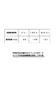
本実施形態で製造されるフィルム状データキャリアの耐湿試験結果(温度85°C,湿度85%)を図13に示す。同図に示されるように、耐湿試験250時間経過後の通信距離の変動は±10%以内であり、バンプ接続部分の耐湿信頼性としては十分な値が得られることが確認された。
【0111】
【発明の効果】
以上の説明で明らかなように、この発明によれば、配線基板上に半導体チップを迅速に、電気的にも機械的にも確実に、さらに低コストに、実装可能なフリップチップ接続方式による半導体チップの実装方法を提供することができる。
【0112】
また、この発明によれば、航空タグ、物流管理用ラベル、無人改札用パス等として機能する電磁波読み取り可能なデータキャリアを低コストに大量生産することが可能な電磁波読み取り可能なデータキャリアの製造方法を提供することができる。
【図面の簡単な説明】
【図1】本発明実装方法を説明する工程図である。
【図2】超音波実装工程の詳細を示す説明図である。
【図3】本発明方法による実装構造の断面図である。
【図4】半導体チップと配線パターンとの接合強度を表にして示す図である。
【図5】データキャリアの一例を示す正面図である。
【図6】データキャリア本体と電磁部品モジュールとの積層部の断面図である。
【図7】データキャリア本体の製造工程を示す工程図である。
【図8】電子部品モジュールの製造工程を示す工程図である。
【図9】電子部品モジュールのデータキャリア本体への搭載工程を示す工程図である。
【図10】データキャリア本体の製造工程を示す図である。
【図11】電子部品モジュールの製造工程を示す図である。
【図12】電子部品モジュールのデータキャリア本体への搭載工程を示す工程図である。
【図13】本発明が適用されたフィルム状データキャリアの耐湿試験結果を表にして示す図である。
【図14】フリップチップ接続の第1従来方式を示す図である。
【図15】リップチップ接続の第2従来方式を示す図である。
【符号の説明】
1,401,701 Al−PET積層基材
2,402,702 PETフィルム
3,403,703 アルミ箔
4,404,704 熱可塑性樹脂製のエッチングレジストパターン
5,405,705 レジストパターンの存在しない部分
6,406,706 アルミ箔配線パターン
7,407,707 配線基板
8,408,708 半導体ベアチップ
9,409,709 バンプ
10,410,710 配線パターン上の電極領域
11,801,802 超音波ホーン
12,803,804 ヒータテーブル兼超音波アンビル
DC データキャリア
100 データキャリア本体
101 PET製基体
102 渦巻状導体パターン
102a 周回導体束
103 内周側端子パッド
104 外周側端子パッド
200 電子部品モジュール
201 絶縁性小片
202 ベアチップ
411,711 ポッティング部
412 導電性レジスト領域
501a,501b 圧子[0001]
TECHNICAL FIELD OF THE INVENTION
The present invention relates to a method for mounting a semiconductor chip suitable for manufacturing an electromagnetic wave readable data carrier functioning as an airline tag, a logistics management label, an unmanned ticket gate path, and the like, and in particular, flips a semiconductor bare chip on a wiring board. The present invention relates to a method of mounting a semiconductor chip which can be mounted at low cost by a chip connection method.
[0002]
[Prior art]
As this type of electromagnetic wave readable data carrier, for example, an airline tag described in Japanese Patent Application Laid-Open No. 6-243358 is known. In the near future, this airline tag is expected to be used in a disposable manner for the management of customer luggage at airports, etc., in which case, for example, in the case of a global airline, only one of these airline tags has a monthly production of 850 A huge demand of 10,000 sheets is expected. Therefore, it is desired to establish an ultra-low-cost mass production technology for this type of airline tag.
[0003]
The aeronautical tag described in this publication is configured by mounting a spiral conductive pattern serving as an antenna coil and IC components serving as a transmitting / receiving circuit, a memory, and the like on one surface of a PET film base having a rectangular shape.
[0004]
The aeronautical tag body holding the spiral conductor pattern serving as an antenna coil can be formed by selectively corroding a copper foil or an aluminum foil adhered on one side of a PET film by etching. Therefore, a continuous production line based on RTR (Roll To Roll) can be easily realized by a resist forming process using a known photolithography technique and a subsequent wet etching process. On the other hand, circuit components such as a transmitting / receiving circuit and a memory to be mounted on the airline tag main body are formed into one chip by using a semiconductor integrated technology.
[0005]
The present applicant previously modularized a semiconductor bare chip constituting the above-described transmitting / receiving circuit, memory, and the like by mounting the semiconductor bare chip on a film-like insulating small piece (a kind of wiring board) in advance. It has been proposed to improve the productivity of airline tags by bonding them to a PET film constituting the airline tag body.
[0006]
By the way, in the electronic component mounting sheet that requires a high degree of thinness, such as the above-mentioned electronic component module bonded to an airline tag, a proposal regarding a flip-chip connection method in which a bare semiconductor chip is directly mounted on a wiring board. Has been prosperous.
[0007]
FIG. 14 shows an example of the flip-chip connection method (hereinafter, referred to as a first conventional method). In the first conventional method, a projection-like terminal (hereinafter, referred to as a bump) b for connection is formed in advance on a bottom electrode (not shown) of a semiconductor chip a, and the bump b and the wiring board c are formed. After alignment with the electrode region d of the upper wiring pattern, the two are connected by a bonding material e such as solder or conductive paste.
[0008]
In the first conventional method, (1) the steps of supplying and curing a bonding material e for connecting the bump b and the electrode region d of the wiring pattern are complicated, and (2) the bump connection portion In order to obtain the moisture resistance reliability and the mounting strength of the semiconductor, it is necessary to fill an insulating resin f called an underfill between the chip a and the substrate c to seal the bump connection portion. It is pointed out that a step of filling and curing the insulating resin f becomes necessary, and that the production cost is increased due to the above.
[0009]
Another example of the flip-chip connection method (hereinafter, referred to as a second conventional method) is shown in FIG. The second conventional method solves the problem of the first conventional method, and uses a semiconductor bare chip on a wiring board using an anisotropic conductive sheet as proposed in Japanese Patent No. 2,586,154. Is to implement.
[0010]
In the second conventional method, an anisotropic conductive sheet g in which conductive fine particles are dispersed in a thermoplastic or thermosetting resin is interposed between a semiconductor bare chip a and a wiring board c, and thermocompression bonding is performed. The resin is caused to flow, and electrical connection in the thickness direction is obtained by conductive fine particles h sandwiched between the bump b and the electrode region d of the wiring pattern.
[0011]
In this method, the alignment with the wiring pattern when the semiconductor is mounted on the wiring board can be performed relatively roughly, the resin curing time is as short as 10 to 20 seconds, and a sealing material such as an underfill needs to be used. Therefore, there is an effect that the manufacturing cost can be reduced. On the other hand, (1) the anisotropic conductive sheet g is relatively expensive, and (2) its curing requires a high temperature of 200 ° C. or more, so that it cannot be used for a substrate without heat resistance. (3) Although it takes a relatively short time, it takes 10 to 20 seconds to cure the resin material, and it is difficult to further simplify the process and increase the speed. (4) Between the bump and the substrate pattern Since electrical connection is made by contact of conductive fine particles dispersed in a resin material, problems such as poor connection reliability are still pointed out.
[0012]
[Problems to be solved by the invention]
The present invention has been made by paying attention to the above-mentioned problems in the conventional flip-chip connection method, and an object thereof is to quickly, electrically and mechanically mount a semiconductor chip on a wiring board. An object of the present invention is to provide a method of mounting a semiconductor chip by a flip chip connection method which can be mounted reliably and at a lower cost.
[0013]
Another object of the present invention is to provide a flip-chip connection wiring board suitable for the above mounting method.
[0014]
Another object of the present invention is to provide a method of manufacturing a wiring board for flip-chip connection, which can manufacture the above-described wiring board simply and at low cost.
[0015]
Still another object of the present invention is to provide an electromagnetic wave readable data carrier that can be mass-produced at low cost and function as an airline tag, a label for logistics management, a pass for unmanned ticket gates, and the like. An object of the present invention is to provide a method for manufacturing a data carrier.
[0016]
Still other objects and effects of the present invention will be easily understood by those skilled in the art by referring to the description of the embodiments and the like.
[0017]
[Means for Solving the Problems]
In the method of mounting a semiconductor chip according to the present invention, in a state where a thermoplastic resin film covering an electrode region on a wiring pattern is heated and melted, ultrasonic waves are applied to a bump of a semiconductor bare chip on the thermoplastic resin film in the molten state. By pressing while applying, a step of contacting the bump and the electrode region by pushing away the molten thermoplastic resin film,
In a state where the bump and the electrode region are in contact with each other, by continuously applying ultrasonic waves, a step of ultrasonically bonding the bump and the electrode region,
The step of cooling and solidifying the molten thermoplastic resin, and bonding the semiconductor bare chip body to the wiring board,
Is provided.
[0018]
Here, as is apparent from the statement "in a state where the thermoplastic resin film covering the electrode region on the wiring pattern is heated and melted", the electrode region on the wiring pattern of the wiring board used in the present invention is Has a thermoplastic resin film formed in advance. This coating may cover only the electrode region of the wiring pattern, or may cover the entire surface of the wiring pattern.
[0019]
Here, the “electrode region on the wiring pattern” means a certain small region on the wiring pattern including a position where a terminal or the like of an electronic component is to be connected. This electrode region will include a portion generally called a land or the like on the wiring pattern.
[0020]
The term “heat melting” refers to a concept that includes both a state where the thermoplastic resin film is heated and melted and a state where the thermoplastic resin film is heated and softened to some extent. Furthermore, it is preferable that the “thermoplastic resin” referred to here has good properties as an adhesive.
[0021]
According to such a configuration, (1) since the bonding between the bump and the electrode region is diffusion bonding using ultrasonic waves, reliable electrical conduction can be achieved, and (2) the bonding portion is sealed with resin. Therefore, (3) the semiconductor chip and the wiring board are adhered when the thermoplastic resin is cured, so that the mechanical mounting strength against pulling and the like is high, and Electrical conduction and mechanical coupling can be simultaneously performed in a short time, (5) a special sealing or bonding step, and a low manufacturing cost because no adhesive material is required; (6) the substrate surface is exposed Since the thermoplastic resin film does not exist in the portion where it is present, the effects such as that the substrate surface is not unnecessarily sticky during heating can be obtained.
[0022]
Also, in the flip-chip connection wiring board of the present invention, the surface of the wiring pattern is entirely covered with a thermoplastic resin film.
[0023]
According to such a configuration, when used in the above-described mounting method, the surface of the wiring pattern is covered with the thermoplastic resin coating over the entire surface, so that the sealing structure having good moisture resistance and the tensile strength are provided. A high bonding structure is obtained.
[0024]
In the method of manufacturing a wiring substrate for flip chip connection according to the present invention, a thermoplastic resin is used as an etching mask material used when forming a wiring pattern by etching.
[0025]
According to such a configuration, the etching mask material used in the etching process for forming the wiring pattern becomes a thermoplastic resin film covering the entire surface of the conductor pattern as it is, so that a separate film forming step is not required and time is required. It can be manufactured at low cost without hanging.
[0026]
Further, the method of manufacturing a data carrier capable of reading electromagnetic waves according to the present invention comprises: a data carrier main body in which a spiral conductive pattern forming an antenna coil is held on a film-shaped, sheet-shaped, or thin-plate-shaped insulating base; A method for manufacturing an electromagnetic wave readable data carrier that is integrated with an electronic component module in which a semiconductor bare chip constituting a transmission / reception circuit, a memory, and the like is mounted on a wiring pattern of a shape, a sheet, or a thin wiring substrate. .
[0027]
In this method of manufacturing a data carrier, a main characteristic point is a step of manufacturing an electronic component module in which a semiconductor bare chip is mounted on a wiring pattern of the film, sheet, or thin wiring board.
[0028]
That is, in the step of manufacturing the electronic component module, in a state where the thermoplastic resin coating covering the electrode region on the wiring pattern is heated and melted, the bumps of the semiconductor bare chip are placed on the thermoplastic resin coating in the molten state. By pressing while applying an ultrasonic wave, a step of pushing out the molten thermoplastic resin film and contacting the bump and the electrode region, and continuously applying ultrasonic waves in a state where the bump and the electrode region are in contact with each other This includes a step of ultrasonically bonding the bump and the electrode region to each other, and a step of cooling and solidifying the molten thermoplastic resin to adhere the semiconductor bare chip body to the wiring substrate.
[0029]
According to such a configuration, since (1) the bonding between the bump and the electrode region is diffusion bonding using ultrasonic waves, reliable electrical conduction can be achieved, and (2) the bonding portion is resin-sealed. (3) that the semiconductor chip and the wiring board are adhered to each other when the thermoplastic resin is cured, so that the mechanical mounting strength against pulling and the like is high; ) Electrical conduction and mechanical coupling can be simultaneously performed in a short time; (5) the production cost is low because no special sealing or bonding step or material is required; and (6) the substrate surface is exposed. Electromagnetic waves that function as air tags, logistics management labels, unmanned ticket gates, etc. through the effects such as the fact that there is no thermoplastic resin coating on the parts, so that the substrate surface does not stick more than necessary when heated. Readable The such data carrier it is possible to mass-produced at a low cost.
[0030]
In the wiring board used in the manufacturing process of the electronic component module of the present invention, the entire surface of the wiring pattern is covered with a thermoplastic resin film.
[0031]
According to such a configuration, when used in the above-described process of manufacturing the electronic component module, the surface of the wiring pattern is covered with the thermoplastic resin film over the entire surface, so that the sealing with good moisture resistance is achieved. A structure and an adhesive structure having high tensile strength can be obtained.
[0032]
In the method for manufacturing a wiring board according to the present invention, a thermoplastic resin is used as an etching mask material used when forming a wiring pattern by etching.
[0033]
According to such a configuration, the etching mask material used in the etching process for forming the wiring pattern becomes a thermoplastic resin film covering the entire surface of the conductor pattern as it is, so that a separate film forming step is not required and time is required. It can be manufactured at low cost without hanging.
[0034]
Further, the method of manufacturing an electromagnetic wave readable data carrier according to the present invention includes a data carrier main body in which a metal foil pattern constituting an antenna coil is held on a film-shaped resin base; This is a method of manufacturing an electromagnetic wave readable data carrier integrally formed with an electronic component module in which a semiconductor bare chip constituting a transmission / reception circuit, a memory, or the like is mounted on a pattern.
[0035]
In the method of manufacturing a data carrier capable of reading electromagnetic waves, a main characteristic point is a process of manufacturing an electronic component module in which a semiconductor bare chip is mounted on an aluminum foil wiring pattern on the surface of the film-shaped resin base.
[0036]
That is, in the step of manufacturing this electronic component module, in a state where the thermoplastic resin coating covering the electrode region on the aluminum foil wiring pattern is heated and melted, the semiconductor bare chip is placed on the molten thermoplastic resin coating. By pressing the bumps while applying ultrasonic waves, a step of displacing the molten thermoplastic resin film to make contact between the bumps and the electrode regions, and in a state where the bumps and the electrode regions are in contact, ultrasonic waves are continuously applied. And a step of ultrasonically bonding the bump and the electrode region, and a step of cooling and solidifying the molten thermoplastic resin to adhere the semiconductor bare chip body to the wiring board.
[0037]
Further, in the wiring board of the present invention, the surface of the aluminum foil wiring pattern is entirely covered with a thermoplastic resin film.
[0038]
In the method for manufacturing a wiring board according to the present invention, a thermoplastic resin is used as an etching mask material used when forming an aluminum foil wiring pattern by etching.
[0039]
In a preferred embodiment of the present invention, a polyolefin resin or a polyester resin is used as the thermoplastic resin.
[0040]
By using such a resin, it is possible to obtain a good chemical resistance as an etching mask and a good bonding strength between a metal bump on a semiconductor chip side and a metal electrode region on a wiring pattern side. The effect is expected. That is, the polyolefin resin is an alkaline etching solution such as NaOH, and the polyester resin is
[0041]
BEST MODE FOR CARRYING OUT THE INVENTION
Hereinafter, a preferred embodiment of a semiconductor chip mounting method according to the present invention will be described in detail with reference to the accompanying drawings.
[0042]
As described above, the method for mounting a semiconductor chip of the present invention includes the steps of: heating and melting a thermoplastic resin film covering an electrode region on a wiring pattern; By pressing the bare chip bumps while applying ultrasonic waves, a step of pushing out the molten thermoplastic resin coating and bringing the bumps into contact with the electrode regions, and continuing the ultrasonic wave in a state where the bumps and the electrode regions are in contact with each other The step of ultrasonically bonding the bump and the electrode region, and the step of cooling and solidifying the molten thermoplastic resin to adhere the semiconductor bare chip body to the wiring substrate. is there.
[0043]
An outline of a series of steps including such a mounting method is shown in the step diagram of FIG. In this series of steps, a metal foil laminated material manufacturing step (A), an etching mask printing step (B), an etching step (C) for forming a wiring pattern, an ultrasonic mounting step (D), and an adhesion step (E) ) And is included. Hereinafter, details of those steps will be described in order.
[0044]
[Metal foil laminated material manufacturing process (A)]
In this step, an Al-PET
[0045]
[Etching mask printing step (B)]
In this step, an etching resist
[0046]
[Etching step (C)]
In this step, the
[0047]
[Ultrasonic mounting process (D)]
In this step, the semiconductor
[0048]
That is, the semiconductor
[0049]
In the first and second steps described above, after the semiconductor
[0050]
The details of the ultrasonic mounting process are shown in the process diagram of FIG. In the positioning step shown in FIG. 2A, in a state where the
[0051]
In the step of removing the thermoplastic resin adhesive shown in FIG. 4B, the ultrasonic vibration (63.5 KHz, 2 W) is generated by the
[0052]
In the ultrasonic bonding step shown in FIG. 4C, the ultrasonic vibration v is continuously applied, so that the diffusion bonding between the metals is advanced, and the
[0053]
Returning to FIG. 1 again, the description will be continued.
[Adhesion process (E)]
In this step, by removing the heating of 150 ° C. applied to the wiring board, the melted
[0054]
FIG. 3 shows a mounting structure completed through the above steps (A) to (E). As shown in the figure, according to this mounting structure, (1) reliable electrical conduction can be achieved because the bonding between the
[0055]
FIG. 4 shows the bonding strength between the semiconductor
[0056]
In the above-described embodiment, the
[0057]
As the material of the etching resist
[0058]
The
[0059]
According to such a configuration, when used in the above-described mounting method, the surface of the
[0060]
In addition, the method of manufacturing a wiring substrate shown in FIGS. 1B and 1C uses a thermoplastic resin as an etching mask material used when forming a wiring pattern by etching. Therefore, it can be generalized as a method for manufacturing a wiring board for flip chip connection.
[0061]
According to such a configuration, since the etching mask material used for the etching process for forming the wiring pattern becomes the thermoplastic resin film covering the entire surface of the conductor pattern as it is, a separate film forming step is unnecessary. It requires no effort and can be manufactured at low cost.
[0062]
Finally, the operational effects of the semiconductor chip mounting method according to this embodiment will be described together. That is, according to the above mounting method,
(1) In the step of forming a wiring pattern, it is not necessary to separate the insulating resist used in the etching process in a separate step, and the cost can be reduced.
[0063]
(2) Further, the insulating resist made of a thermoplastic resin acts as an adhesive immediately below the semiconductor chip, and the semiconductor mounting strength by ultrasonic waves can be reinforced.
[0064]
(3) Further, the periphery of the bump can be sealed with a resin material, and the reliability of the bump connection at the moisture resistance can be improved.
[0065]
(4) The resin material having the above-mentioned purpose, which is required in the conventional method, is unnecessary, and the material cost can be reduced.
[0066]
(5) A reliable connection between terminals can be obtained by diffusion bonding of a metal between a bump and a wiring pattern by ultrasonic vibration.
[0067]
(6) Ultrasonic bonding, melting and curing of the thermoplastic resin can be performed within 1 to 2 seconds, and the production time can be shortened.
[0068]
Next, an embodiment of a method for manufacturing a data carrier according to the present invention will be described with reference to FIGS. This data carrier can read electromagnetic waves that function as an airline tag, a distribution management label, an unmanned ticket gate pass, and the like. The data carrier includes a data carrier body in which a metal foil pattern constituting an antenna coil is held on a film-shaped resin base, and a transmission / reception circuit, a memory, and the like are formed in an aluminum foil wiring pattern on the surface of the film-shaped resin base. And an electronic component module having a semiconductor bare chip mounted thereon.
[0069]
One example of a data carrier embodiment is shown in FIG. As shown in the figure, this data carrier DC is obtained by holding a spirally conductive pattern (corresponding to an antenna coil) 102 made of copper foil having a thickness of 10 μm on one side of a
[0070]
An example of a mounting structure of the
[0071]
FIG. 7 shows an example of a manufacturing process of the
[0072]
(Step A)
First, a Cu-PET
[0073]
(Step B)
Next, a spiral etching resist
[0074]
(Step C)
Next, on the surface of the
[0075]
(Step D)
Next, the
[0076]
(Step E)
Lastly, in the present embodiment, a through
[0077]
Next, an example of a production process of the
[0078]
[Metal foil laminated material manufacturing process (A)]
In this step, an Al-PET
[0079]
[Etching mask printing step (B)]
In this step, an etching resist
[0080]
[Etching step (C)]
In this step, the
[0081]
[Ultrasonic mounting process (D)]
In this step, the semiconductor
[0082]
That is, the semiconductor
[0083]
In the first and second steps described above, after the semiconductor
[0084]
[Adhesion process (E)]
In this step, by removing the heating of 150 ° C. applied to the wiring board, the melted
[0085]
Next, the
[0086]
(Step A)
First, the electronic component mounting surface of the
[0087]
(Step B)
Next, the
[0088]
Next, another embodiment of the method for manufacturing a data carrier according to the present invention will be described with reference to FIGS. This data carrier is also capable of reading electromagnetic waves that functions as an airline tag, a logistics management label, an unmanned ticket gate pass, and the like. The data carrier includes a data carrier main body in which a metal foil pattern forming an antenna coil is held on a film-shaped resin base in the same manner as the previous example described with reference to FIG. An electronic component module in which a semiconductor bare chip constituting a transmitting / receiving circuit, a memory, or the like is mounted on an aluminum foil wiring pattern on the surface of the base is integrated.
[0089]
FIG. 10 shows an example of a manufacturing process of the spiral conductor pattern 102 (FIG. 5) constituting the antenna coil. With reference to the figure, a process for forming a spiral conductive pattern 102 (FIG. 5) serving as an antenna coil on one side of a PET film base 101 (FIG. 5) will be described.
[0090]
(Step A)
First, the Cu-PET
[0091]
(Step B)
Next, a spiral-shaped and terminal-shaped etching resist
[0092]
(Step C)
By removing the
[0093]
Thereafter, generally, the electronic component cannot be mounted on a circuit, that is, a coil unless the insulating etching resist 604 formed in the step (B) is removed. Since the etching resist located at the
[0094]
Next, an example of a production process of the
[0095]
[Metal foil laminated material manufacturing process (A)]
In this step, an Al-PET
[0096]
[Etching mask printing step (B)]
In this step, an etching resist
[0097]
[Etching step (C)]
In this step, the
[0098]
[Ultrasonic mounting process (D)]
In this step, the semiconductor
[0099]
That is, the semiconductor
[0100]
In the first and second steps described above, after the semiconductor
[0101]
[Adhesion process (E)]
In this step, by removing the heating of 150 ° C. applied to the wiring board, the molten
[0102]
Next, a process of mounting the
[0103]
(Step A)
First, the
[0104]
(Step B)
Next, a pair of
[0105]
Generally, welding is performed by bringing the atoms close to each other (a few angstroms) so that the attractive force works between the atoms on the surface of the metal to be bonded, and by bringing the atoms in the entire surface into contact in an ordered arrangement. Occurs. However, since the surface of the metal is usually covered with a thin surface layer such as an oxide or an adsorbed gas, access of a clean base metal atom is hindered and sufficient bonding force is not generated.
[0106]
Therefore, in this ultrasonic bonding method, the metal surface layer is removed by ultrasonic vibration according to the method described above, and the atoms are further diffused by energizing the atomic vibration, so that the terminal of the electronic component module and the terminal on the antenna coil side are diffused. Is adhesively fixed.
[0107]
Further, as described above, the present method is based on the principle of realizing the bonding by removing the metal surface layer by ultrasonic vibration, and the step (B) of FIG. 12 is performed on the
[0108]
In the embodiment described above, for example, while providing a large number of irregularities corresponding to the shape of the fused portion on the end faces of the
[0109]
Since the film-shaped data carrier completed in this way uses an electromagnetic field as a reading medium, it is not so much restricted in the distance and direction in reading, and specifically, in the reading direction. The data stored in the semiconductor can be reliably read from a distance of 100 to 1000 mm without receiving the data.
[0110]
FIG. 13 shows the results of a moisture resistance test (temperature: 85 ° C., humidity: 85%) of the film-shaped data carrier manufactured in this embodiment. As shown in the figure, the fluctuation of the communication distance after the elapse of 250 hours in the moisture resistance test was within ± 10%, and it was confirmed that a sufficient value was obtained as the moisture resistance reliability of the bump connection portion.
[0111]
【The invention's effect】
As is apparent from the above description, according to the present invention, the semiconductor chip on the wiring board can be mounted quickly, electrically and mechanically reliably, and at a low cost, by a flip-chip connection type semiconductor. A method for mounting a chip can be provided.
[0112]
Further, according to the present invention, a method of manufacturing an electromagnetic wave readable data carrier capable of mass-producing low-cost electromagnetic wave readable data carriers functioning as air tags, distribution management labels, unmanned ticket gates, and the like. Can be provided.
[Brief description of the drawings]
FIG. 1 is a process diagram illustrating a mounting method of the present invention.
FIG. 2 is an explanatory diagram showing details of an ultrasonic mounting process.
FIG. 3 is a sectional view of a mounting structure according to the method of the present invention.
FIG. 4 is a table showing the bonding strength between a semiconductor chip and a wiring pattern;
FIG. 5 is a front view showing an example of a data carrier.
FIG. 6 is a sectional view of a laminated portion of a data carrier main body and an electromagnetic component module.
FIG. 7 is a process chart showing a manufacturing process of the data carrier main body.
FIG. 8 is a process chart showing a manufacturing process of the electronic component module.
FIG. 9 is a process chart showing a process of mounting the electronic component module on the data carrier main body.
FIG. 10 is a diagram showing a manufacturing process of the data carrier main body.
FIG. 11 is a diagram showing a manufacturing process of the electronic component module.
FIG. 12 is a process chart showing a process of mounting the electronic component module on the data carrier main body.
FIG. 13 is a table showing the results of a moisture resistance test of a film data carrier to which the present invention is applied.
FIG. 14 is a diagram showing a first conventional method of flip chip connection.
FIG. 15 is a diagram showing a second conventional method of lip chip connection.
[Explanation of symbols]
1,401,701 Al-PET laminated base material
2,402,702 PET film
3,403,703 Aluminum foil
4,404,704 Etching resist pattern made of thermoplastic resin
5,405,705 Part where resist pattern does not exist
6,406,706 Aluminum foil wiring pattern
7,407,707 Wiring board
8,408,708 Semiconductor bare chip
9,409,709 Bump
10,410,710 Electrode area on wiring pattern
11,801,802 Ultrasonic horn
12,803,804 Heater table and ultrasonic anvil
DC data carrier
100 Data carrier body
101 PET base
102 Spiral conductor pattern
102a orbiting conductor bundle
103 Inner peripheral terminal pad
104 Outer terminal pad
200 Electronic component module
201 insulating piece
202 bare chip
411,711 Potting section
412 conductive resist area
501a, 501b Indenter
Claims (6)
前記バンプと電極領域とが接触した状態において、バンプに超音波振動を継続的に付与することにより生じる摩擦によって前記電極領域の表面の酸化物層を除去すると共に、バンプと電極領域との金属融着部を形成する工程と、
前記溶融した熱可塑性樹脂を冷却固化させて、半導体ベアチップ本体を配線基板上に接着させる工程と、
を具備する半導体チップの実装方法。In a state where the thermoplastic resin film covering the electrode region on the wiring pattern is heated and melted, the semiconductor bare chip bumps are pressed onto the thermoplastic resin film in the melted state while applying ultrasonic vibration, thereby being melted. A step of contacting the bump and the electrode region by displacing the thermoplastic resin film,
In a state where the bump and the electrode region are in contact with each other, the oxide layer on the surface of the electrode region is removed by friction generated by continuously applying ultrasonic vibration to the bump, and a metal fusion between the bump and the electrode region is performed. A step of forming an attachment portion;
The step of cooling and solidifying the molten thermoplastic resin, and bonding the semiconductor bare chip body to the wiring board,
A mounting method of a semiconductor chip comprising:
前記バンプと電極領域とが接触した状態において、バンプと前記電極領域の接触面に平行な方向に超音波振動を継続的に付与することにより生じる摩擦によって前記電極領域の表面の酸化物層を除去すると共に、バンプと電極領域との金属融着部を形成する工程と、
前記溶融した熱可塑性樹脂を冷却固化させて、半導体ベアチップ本体を配線基板上に接着させる工程と、
を具備する半導体チップの実装方法。In a state where the thermoplastic resin film covering the electrode region on the wiring pattern is heated and melted, the bump of the semiconductor bare chip is formed on the thermoplastic resin film in the melted state, and the contact surface between the bump and the thermoplastic resin film is formed. By pressing while applying ultrasonic vibration in a parallel direction, a step of pushing out the molten thermoplastic resin coating and contacting the bump and the electrode region,
In a state where the bump and the electrode region are in contact with each other, the oxide layer on the surface of the electrode region is removed by friction generated by continuously applying ultrasonic vibration in a direction parallel to the contact surface between the bump and the electrode region. And forming a metal fusion part between the bump and the electrode region,
The step of cooling and solidifying the molten thermoplastic resin, and bonding the semiconductor bare chip body to the wiring board,
A mounting method of a semiconductor chip comprising:
Priority Applications (1)
| Application Number | Priority Date | Filing Date | Title |
|---|---|---|---|
| JP2003009971A JP3584404B2 (en) | 2003-01-17 | 2003-01-17 | Semiconductor chip mounting method |
Applications Claiming Priority (1)
| Application Number | Priority Date | Filing Date | Title |
|---|---|---|---|
| JP2003009971A JP3584404B2 (en) | 2003-01-17 | 2003-01-17 | Semiconductor chip mounting method |
Related Parent Applications (1)
| Application Number | Title | Priority Date | Filing Date |
|---|---|---|---|
| JP33340999A Division JP3451373B2 (en) | 1999-11-24 | 1999-11-24 | Manufacturing method of data carrier capable of reading electromagnetic wave |
Publications (3)
| Publication Number | Publication Date |
|---|---|
| JP2003203946A JP2003203946A (en) | 2003-07-18 |
| JP3584404B2 true JP3584404B2 (en) | 2004-11-04 |
| JP2003203946A5 JP2003203946A5 (en) | 2005-02-17 |
Family
ID=27656086
Family Applications (1)
| Application Number | Title | Priority Date | Filing Date |
|---|---|---|---|
| JP2003009971A Expired - Lifetime JP3584404B2 (en) | 2003-01-17 | 2003-01-17 | Semiconductor chip mounting method |
Country Status (1)
| Country | Link |
|---|---|
| JP (1) | JP3584404B2 (en) |
Cited By (1)
| Publication number | Priority date | Publication date | Assignee | Title |
|---|---|---|---|---|
| WO2012032840A1 (en) | 2010-09-07 | 2012-03-15 | オムロン株式会社 | Method for surface mounting electronic component, and substrate having electronic component mounted thereon |
Families Citing this family (2)
| Publication number | Priority date | Publication date | Assignee | Title |
|---|---|---|---|---|
| JP4438558B2 (en) * | 2003-11-12 | 2010-03-24 | 株式会社日立製作所 | RFID tag manufacturing method |
| JP4251104B2 (en) | 2004-03-31 | 2009-04-08 | 株式会社日立製作所 | RFID tag manufacturing method |
-
2003
- 2003-01-17 JP JP2003009971A patent/JP3584404B2/en not_active Expired - Lifetime
Cited By (1)
| Publication number | Priority date | Publication date | Assignee | Title |
|---|---|---|---|---|
| WO2012032840A1 (en) | 2010-09-07 | 2012-03-15 | オムロン株式会社 | Method for surface mounting electronic component, and substrate having electronic component mounted thereon |
Also Published As
| Publication number | Publication date |
|---|---|
| JP2003203946A (en) | 2003-07-18 |
Similar Documents
| Publication | Publication Date | Title |
|---|---|---|
| JP3451373B2 (en) | Manufacturing method of data carrier capable of reading electromagnetic wave | |
| US7276436B2 (en) | Manufacturing method for electronic component module and electromagnetically readable data carrier | |
| JP3928682B2 (en) | Wiring board bonded body, wiring board bonding method, data carrier manufacturing method, and electronic component module mounting apparatus | |
| WO2001006558A1 (en) | Package of semiconductor device and method of manufacture thereof | |
| JP2004516538A (en) | Smart label web and manufacturing method thereof | |
| JP2005275802A (en) | Method for radio wave readable data carrier, board using the method, and electronic component module | |
| JP2007042087A (en) | Rfid tag and production method therefor | |
| JP3584404B2 (en) | Semiconductor chip mounting method | |
| JP4179736B2 (en) | Manufacturing method of semiconductor element mounted component and manufacturing method of semiconductor element mounted finished product | |
| JP2000299411A (en) | Chip-mounting body and its manufacture | |
| JP2000151057A (en) | Electronic component mounting structure, manufacture thereof, wireless ic card and manufacture thereof | |
| JP2008235840A (en) | Method and apparatus for manufacturing semiconductor device, and semiconductor module | |
| MX2008012339A (en) | Methods for attaching a flip chip integrated circuit assembly to a substrate. | |
| JP2000231614A (en) | Data carrier which can be read by electromagnetic wave | |
| JP2008235839A (en) | Semiconductor device, and manufacturing method therefor | |
| JP2004062634A (en) | Connectless communication device and method for connecting the same | |
| JP5024190B2 (en) | IC module manufacturing method | |
| JPH11134467A (en) | Film for holding electronic parts and its manufacture | |
| JP3827014B2 (en) | Electromagnetic readable data carrier | |
| JP2009258943A (en) | Strap, tag inlet, and rfid tag | |
| JP2014115938A (en) | Semiconductor device and manufacturing method thereof | |
| JP2015219878A (en) | Composite ic card and composite ic card module used for the same | |
| JP2004185229A (en) | Noncontact ic card and its manufacturing method | |
| JP2005108259A5 (en) | ||
| JP2001185583A (en) | Semiconductor mounting device and manufacturing method thereof |
Legal Events
| Date | Code | Title | Description |
|---|---|---|---|
| A521 | Written amendment |
Free format text: JAPANESE INTERMEDIATE CODE: A523 Effective date: 20040310 |
|
| A621 | Written request for application examination |
Free format text: JAPANESE INTERMEDIATE CODE: A621 Effective date: 20040310 |
|
| A871 | Explanation of circumstances concerning accelerated examination |
Free format text: JAPANESE INTERMEDIATE CODE: A871 Effective date: 20040310 |
|
| A975 | Report on accelerated examination |
Free format text: JAPANESE INTERMEDIATE CODE: A971005 Effective date: 20040416 |
|
| A131 | Notification of reasons for refusal |
Free format text: JAPANESE INTERMEDIATE CODE: A131 Effective date: 20040423 |
|
| A521 | Written amendment |
Free format text: JAPANESE INTERMEDIATE CODE: A523 Effective date: 20040615 |
|
| TRDD | Decision of grant or rejection written | ||
| A01 | Written decision to grant a patent or to grant a registration (utility model) |
Free format text: JAPANESE INTERMEDIATE CODE: A01 Effective date: 20040709 |
|
| A61 | First payment of annual fees (during grant procedure) |
Free format text: JAPANESE INTERMEDIATE CODE: A61 Effective date: 20040722 |
|
| R150 | Certificate of patent or registration of utility model |
Ref document number: 3584404 Country of ref document: JP Free format text: JAPANESE INTERMEDIATE CODE: R150 Free format text: JAPANESE INTERMEDIATE CODE: R150 |
|
| FPAY | Renewal fee payment (event date is renewal date of database) |
Free format text: PAYMENT UNTIL: 20080813 Year of fee payment: 4 |
|
| FPAY | Renewal fee payment (event date is renewal date of database) |
Free format text: PAYMENT UNTIL: 20080813 Year of fee payment: 4 |
|
| FPAY | Renewal fee payment (event date is renewal date of database) |
Free format text: PAYMENT UNTIL: 20090813 Year of fee payment: 5 |
|
| FPAY | Renewal fee payment (event date is renewal date of database) |
Free format text: PAYMENT UNTIL: 20100813 Year of fee payment: 6 |
|
| FPAY | Renewal fee payment (event date is renewal date of database) |
Free format text: PAYMENT UNTIL: 20100813 Year of fee payment: 6 |
|
| FPAY | Renewal fee payment (event date is renewal date of database) |
Free format text: PAYMENT UNTIL: 20110813 Year of fee payment: 7 |
|
| FPAY | Renewal fee payment (event date is renewal date of database) |
Free format text: PAYMENT UNTIL: 20110813 Year of fee payment: 7 |
|
| FPAY | Renewal fee payment (event date is renewal date of database) |
Free format text: PAYMENT UNTIL: 20120813 Year of fee payment: 8 |
|
| FPAY | Renewal fee payment (event date is renewal date of database) |
Free format text: PAYMENT UNTIL: 20130813 Year of fee payment: 9 |
|
| EXPY | Cancellation because of completion of term |