EP2612377B1 - Process for preparing an organic electronic device - Google Patents
Process for preparing an organic electronic device Download PDFInfo
- Publication number
- EP2612377B1 EP2612377B1 EP11741411.0A EP11741411A EP2612377B1 EP 2612377 B1 EP2612377 B1 EP 2612377B1 EP 11741411 A EP11741411 A EP 11741411A EP 2612377 B1 EP2612377 B1 EP 2612377B1
- Authority
- EP
- European Patent Office
- Prior art keywords
- cross
- layer
- insulator layer
- osc
- dielectric material
- Prior art date
- Legal status (The legal status is an assumption and is not a legal conclusion. Google has not performed a legal analysis and makes no representation as to the accuracy of the status listed.)
- Active
Links
Images


Classifications
-
- H—ELECTRICITY
- H10—SEMICONDUCTOR DEVICES; ELECTRIC SOLID-STATE DEVICES NOT OTHERWISE PROVIDED FOR
- H10K—ORGANIC ELECTRIC SOLID-STATE DEVICES
- H10K10/00—Organic devices specially adapted for rectifying, amplifying, oscillating or switching; Organic capacitors or resistors having potential barriers
-
- H—ELECTRICITY
- H10—SEMICONDUCTOR DEVICES; ELECTRIC SOLID-STATE DEVICES NOT OTHERWISE PROVIDED FOR
- H10K—ORGANIC ELECTRIC SOLID-STATE DEVICES
- H10K71/00—Manufacture or treatment specially adapted for the organic devices covered by this subclass
- H10K71/10—Deposition of organic active material
- H10K71/12—Deposition of organic active material using liquid deposition, e.g. spin coating
- H10K71/13—Deposition of organic active material using liquid deposition, e.g. spin coating using printing techniques, e.g. ink-jet printing or screen printing
-
- H—ELECTRICITY
- H10—SEMICONDUCTOR DEVICES; ELECTRIC SOLID-STATE DEVICES NOT OTHERWISE PROVIDED FOR
- H10K—ORGANIC ELECTRIC SOLID-STATE DEVICES
- H10K71/00—Manufacture or treatment specially adapted for the organic devices covered by this subclass
- H10K71/10—Deposition of organic active material
- H10K71/191—Deposition of organic active material characterised by provisions for the orientation or alignment of the layer to be deposited
-
- H—ELECTRICITY
- H10—SEMICONDUCTOR DEVICES; ELECTRIC SOLID-STATE DEVICES NOT OTHERWISE PROVIDED FOR
- H10K—ORGANIC ELECTRIC SOLID-STATE DEVICES
- H10K10/00—Organic devices specially adapted for rectifying, amplifying, oscillating or switching; Organic capacitors or resistors having potential barriers
- H10K10/40—Organic transistors
- H10K10/46—Field-effect transistors, e.g. organic thin-film transistors [OTFT]
- H10K10/462—Insulated gate field-effect transistors [IGFETs]
- H10K10/468—Insulated gate field-effect transistors [IGFETs] characterised by the gate dielectrics
- H10K10/471—Insulated gate field-effect transistors [IGFETs] characterised by the gate dielectrics the gate dielectric comprising only organic materials
-
- H—ELECTRICITY
- H10—SEMICONDUCTOR DEVICES; ELECTRIC SOLID-STATE DEVICES NOT OTHERWISE PROVIDED FOR
- H10K—ORGANIC ELECTRIC SOLID-STATE DEVICES
- H10K10/00—Organic devices specially adapted for rectifying, amplifying, oscillating or switching; Organic capacitors or resistors having potential barriers
- H10K10/40—Organic transistors
- H10K10/46—Field-effect transistors, e.g. organic thin-film transistors [OTFT]
- H10K10/462—Insulated gate field-effect transistors [IGFETs]
- H10K10/464—Lateral top-gate IGFETs comprising only a single gate
-
- H—ELECTRICITY
- H10—SEMICONDUCTOR DEVICES; ELECTRIC SOLID-STATE DEVICES NOT OTHERWISE PROVIDED FOR
- H10K—ORGANIC ELECTRIC SOLID-STATE DEVICES
- H10K10/00—Organic devices specially adapted for rectifying, amplifying, oscillating or switching; Organic capacitors or resistors having potential barriers
- H10K10/40—Organic transistors
- H10K10/46—Field-effect transistors, e.g. organic thin-film transistors [OTFT]
- H10K10/462—Insulated gate field-effect transistors [IGFETs]
- H10K10/466—Lateral bottom-gate IGFETs comprising only a single gate
-
- H—ELECTRICITY
- H10—SEMICONDUCTOR DEVICES; ELECTRIC SOLID-STATE DEVICES NOT OTHERWISE PROVIDED FOR
- H10K—ORGANIC ELECTRIC SOLID-STATE DEVICES
- H10K71/00—Manufacture or treatment specially adapted for the organic devices covered by this subclass
- H10K71/10—Deposition of organic active material
- H10K71/12—Deposition of organic active material using liquid deposition, e.g. spin coating
-
- H—ELECTRICITY
- H10—SEMICONDUCTOR DEVICES; ELECTRIC SOLID-STATE DEVICES NOT OTHERWISE PROVIDED FOR
- H10K—ORGANIC ELECTRIC SOLID-STATE DEVICES
- H10K71/00—Manufacture or treatment specially adapted for the organic devices covered by this subclass
- H10K71/40—Thermal treatment, e.g. annealing in the presence of a solvent vapour
-
- H—ELECTRICITY
- H10—SEMICONDUCTOR DEVICES; ELECTRIC SOLID-STATE DEVICES NOT OTHERWISE PROVIDED FOR
- H10K—ORGANIC ELECTRIC SOLID-STATE DEVICES
- H10K77/00—Constructional details of devices covered by this subclass and not covered by groups H10K10/80, H10K30/80, H10K50/80 or H10K59/80
- H10K77/10—Substrates, e.g. flexible substrates
Definitions
- the present invention relates to a process for preparing improved electronic devices, in particular organic field effect transistors (OFETs), with patterned insulator and organic semiconductor layers.
- OFETs organic field effect transistors
- OFETs Organic field effect transistors
- OFETs are used in display devices and logic capable circuits. For many display applications a high on/off ratio is required so that sufficient contrast and a reliable dynamic operation is obtained. Improvements in the on/off ratio have been achieved in the past by patterning of the organic semiconductor (OSC) layer to reduce parasitic leakage currents, as disclosed for example in US 5,854,139 .
- the semiconductor layer may be patterned by conventional lithography using an etching step to remove the layer from unwanted areas. Such techniques are well established in inorganic electronics.
- organic semiconductors (OSC) are often not easily processed by etching. For example the OSC layer may be deposited by inkjet on active areas only.
- US 5,854,139 discusses patterning an oligothiophene OSC by illuminating the OSC layer through an optical mask.
- WO 2006/048092 A1 suggests a process for patterning the OSC layer by applying an oxidizing agent to the OSC layer outside the channel areas, and reports that this leads to an improved on/off ratio.
- JP-A-2007-156782 discloses a thin film transistor, wherein the gate electrode is formed on a substrate, the gate dielectric film is constituted by a cross-linkable photosensitive material and formed so that the gate electrode may be covered, a semiconductor layer is laminated on the gate dielectric film, and source and drain electrode are formed such that they are in contact with the semiconductor layer. a passivation layer is formed so that the semiconductor layer, the source electrode and the drain electrode are covered, and an ITO electrode is formed.
- WO 2004/102690 A2 discloses depositing a photopatternable polymer solution onto a silicon wafer, dry-spinning the wafer, baking at 80°C for 5 minutes on a hot plate, placing a silicon shadow mask on top of the substrate, exposing the substrate to UV to crosslink the polymer in the exposed regions, removing the shadow mask, and exposing the substrate to a post-exposure bake at 150°C for 5 seconds on a hot plate and then at 165°C for 2 minutes to complete the cross-linking.
- Another method reported for patterning the OSC layer suggested in prior art is based on varying the surface energy (wettability) of the surface around a transistor device. This concept of directing or confining a deposited drop via a surface energy gradient is a well known principle and is reported as being especially suitable for inkjet printing processes, as described for example in Appl. Phys. Lett. 79, 3536 (2001 ).
- OE organic electronic
- an OSC layer with a crystallization pattern comprising regions having a high degree of crystallinity that exhibit high charge carrier mobility and regions having a low degree of crystallinity or even being amorphous that exhibit low charge carrier mobility.
- This can be simply achieved by providing an insulator layer onto which the OSC layer is subsequently applied, wherein the insulator layer contains a cross-linkable material, and wherein the cross-linking density in specific regions can be varied for example by UV irradiation through a shadow mask.
- Coating the processed insulator layer with an OSC formulation results in the formation of OSC crystals on the surface of the insulator layer only in regions which have been subjected to increased UV irradiation. On the other regions of the insulator layer the coated OSC will be amorphous or have a lower degree of crystallinity.
- the invention relates to a process of preparing an organic electronic (OE) device, comprising the steps of
- the process comprises, before the first exposure step, the step of partially cross-linking the dielectric material in one or more, but not all, areas of the insulator layer, thereby providing a pattern of areas that are cross-linked and areas that are not cross-linked, wherein the cross-linking of the dielectric material is preferably sufficient to provide solvent resistance.
- the process according to this preferred embodiment further comprises, after the first and second exposure steps, the step of removing any remaining dielectric material that was not cross-linked in the previous steps, for example by a solvent rinse.
- the invention further relates to an organic electronic (OE) device obtainable or obtained by a process as described above and below, preferably a top gate organic field effect transistor (OFET).
- OE organic electronic
- OFET top gate organic field effect transistor
- dielectric and "insulating” or “insulator” are used above and below interchangeably.
- reference to an insulator layer also includes a dielectric layer and vice versa.
- interlayer means a layer in an organic electronic device which is provided between two other functional layers or components of the device, for example between the gate insulator layer and the gate electrode, or between the gate insulator layer and the semiconductor layer.
- the area between the source electrode and the drain electrode, which is being covered by or being superposed to a gate electrode in an OFET device, is also referred to as the "channel area”.
- polymer generally means a molecule of high relative molecular mass, the structure of which essentially comprises the multiple repetition of units derived, actually or conceptually, from molecules of low relative molecular mass (see Pure Appl. Chem., 1996, 68, 2289 ).
- repeating unit or “monomeric unit” means the constitutional repeating unit (CRU), which is the smallest constitutional unit the repetition of which a regular macromolecule, a regular oligomer molecule, a regular block or a regular chain (see Pure Appl. Chem., 1996, 68, 2291 ).
- UV radiation should be understood to include any type radiation of a specific wavelength or wavelength range that may be used to induce a cross-linking reaction in a cross-linkable material according to the present invention, for example UV radiation.
- a cross-linkable material according to the present invention is cross-linkable by exposure to UV radiation, and the photoradiation used in the process of the present invention is UV radiation.
- any embodiment of a process as described above and below which refers to UV radiation may also be adapted to another type of photoradiation, for example radiation with a wavelength in the visible or infrared (IR) range, depending on the type of cross-linkable materials used.
- radiation dosage means the amount of radiation power (W) over a given area (cm 2 ) applied to a sample for a given time (s).
- the dosage is given in units of J/cm 2 and is usually defined for a specific wavelength or over a specific range of wavelengths.
- area and region are used interchangeably to describe a certain part of a device layer like the insulator layer or the OSC layer.
- the process according to the present invention preferably uses materials based on cross-linking, like for example [2+2] cross-linking, which may be photoinduced or thermally induced or a combination of both, as insulators, in particular as organic gate insulator (OGI), in an OE device, preferably an OFET.
- insulators in particular as organic gate insulator (OGI), in an OE device, preferably an OFET.
- OGI organic gate insulator
- the cross-linking density in specific regions of the insulator layer can be varied by irradiation through a shadow mask, so that different regions are exposed to different radiation dosages.
- the insulator layer exhibits a pattern of regions that have been exposed only to the first or second radiation dosage and regions that have been exposed both to the first and the second radiation dosage.
- Coating the processed and patterned insulator layer with a spin coated OSC formulation will then result in the formation of crystals of the OSC material on the surface of the insulator only in regions which have been exposed to an increased UV radiation dosage. In contrast thereto, on the other regions of the insulator layer, which have been exposed to lower radiation dosage, it is observed that the coated OSC material forms an amorphous or less crystalline layer.
- the method of creating an OSC layer with a crystallisation pattern according to the present invention is not based on changing the surface energy by photoirradiation, as disclosed for example in US 2007/0096088 A1 . Also, the surface energy does not change significantly and there is no new surface chemistry introduced.
- the inventors of the present invention believe that the patterned crystallisation observed in the OSC layer as described above and below is related to the cross-linking density of the insulator layer onto which the OSC layer is deposited.
- a certain hardness is required for OSC crystals to be formed on the surface of the insulator, hereby the hardness is linked to the cross-linking density.
- the corresponding cross-linking density R C where crystals begin to form is significantly higher than the cross-linking density R S necessary to achieve insolubility of the insulator.
- the coated OSC formulations are resulting in amorphous non-crystalline films.
- cross-linkable polymeric insulator materials based e.g. on 2+2-coupling chemistry (or other bimolecular cross-linking reactions)
- the cross-linking density can be easily controlled by the amount of incident photons (e.g. the radiation dosage) provided to the system.
- the cross-linking chemistry is preferably based on individual and nearly independent bi-molecular 2+2 coupling reactions without any self-propagating effect and not on a chain reaction.
- the inventors of the present invention do further believe that the formation of OSC crystals is linked to the amount of swelling and/or penetration of the insulator layer surface by the OSC formulation deposited onto the OGI layer in a subsequent device manufacturing step.
- the process according to the present invention can be advantageously used for example to decrease the off-current in OFET devices by confining OSC crystal formation solely to the channel area.
- This allows area-coating techniques such as spin coating to recreate the low off-currents of patterned deposition methods such as IJP.
- it can be used in combination with other patterning methods to increase resolution for example of flexographic printing. Thereby the resolution of those printing techniques will be lower than the transistor feature sizes, so that the process of the present invention can also be used for fine-tuning and/or improving positional accuracy. Therefore, it may be that no further layers, such as bank structures, are needed.
- UV irradiation usually enables positional patterning of the subsequent OSC layer (e.g. by solvent based deposition, usually using ink-jet printing) by varying the surface energy (or wettability) of the surface around a transistor device.
- This concept of directing or confining a deposited drop via a surface energy gradient is a well known principle and is described for example in Appl. Phys. Lett. 79, 3536 (2001 ).
- the wettability/surface energy of the substrate i.e. the OGI
- the wettability/surface energy of the substrate itself is not significantly affected by the photoradiation, as the irradiation does not lead to any chemical change except for the intended cross-linking reaction.
- the effect of the different radiation dosages is to produce regions with different cross-linking density of the insulator.
- the OSC is deposited over the whole area of the device and not physically patterned by depositing the OSC only into the active transistor device area.
- the process can thus be described as "simulated" patterning, and is especially advantageous for low-resolution printing methods like e.g. flexo-printing or gravure-printing, where large areas are covered by the OSC, and where surface energy induced patterning concepts are not efficient in confining the relatively high amount of ink deposited.
- the method according to the present invention provides further advantages. For example, in ink-jet printing, if a drop is deposited into the channel it is usually larger than the channel region if no bank structure is used.
- the channel areas can be defined as the crystallisation area, and therefore, although the drop still covers a large region, crystallisation will only take place in the patterned channel region. This can lead to improved crystal morphology in devices prepared by ink-jet printing, and can eliminate at least some of the detrimental morphologies seen when ink-jetted drops undergo the so-called "coffee stain effect".
- Another advantage is that a low resolution process such as flexoprinting can be used to create high resolution patterned channels, without the complexity of removing the OSC material, or the cost of a higher resolution technique.
- partial cross-linking and “partially cross-linked” as used above and below mean that not all, but only a portion, of the cross-linkable moieties in the cross-linkable dielectric material will react by a cross-linking reaction, for example upon exposure to a first radiation dosage.
- “Further cross-linking " or “higher degree of cross-linking” means that at least some of the cross-linkable moieties, which have not reacted in the previous irradiation step, will react by a cross-linking reaction for example in a subsequent irradiation step and/or in an annealing step.
- step a) a step of cleaning the substrate is carried out before step a) and a surface treatment can be applied to increase adhesion between the substrate and insulator layer can be applied.
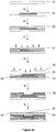
- Figure 1A is a schematic representation of a typical BG, bottom contact OFET according to prior art, including a gate electrode (2) provided on a substrate (1), a layer of dielectric material (3) (gate insulator layer), source (S) and drain (D) electrodes (5), a layer of OSC material (4), and an optional second insulator or protection layer (6) to shield or protect the OSC layer and the S/D electrodes from further layers or devices that may be later provided thereon or from environmental influence.
- the distance between the source and drain electrodes (5) is the channel area.
- Figure 1B is a schematic representation of a typical BG, top contact OFET according to prior art, including a gate electrode (2) provided on a substrate (1), a layer of dielectric material (3) (gate insulator layer), a layer of OSC material (4), source (S) and drain (D) electrodes (5), and an optional protection layer (6) to shield or protect the OSC layer and the S/D electrodes from further layers or from environmental influence.
- Figure 2 is a schematic representation of a typical TG OFET according to prior art, including source and drain electrodes (5) provided on a substrate (1), a layer of OSC material (4), a layer of dielectric material (3) (gate insulator layer), a gate electrode (5), and an optional second insulator or protection layer (6) to shield the gate electrode from further layers or devices that may be later provided.
- Figure 3A exemplarily and schematically illustrates a comparable process, not in accordance with the present invention, for preparing a bottom gate, bottom contact OFET device in accordance with the present invention.
- the reference numbers of a layer provided in a single step as shown in Figure 3A are not always displayed in the next step.
- a gate electrode (20) is deposited onto a substrate (10), the surface of which has preferably been cleaned before depositing the gate electrode.
- a layer of cross-linkable dielectric material (30) is deposited onto the gate electrode to serve as gate insulator layer.
- a photo-patterning step b1) wherein the dielectric material is masked and subjected to photoradiation, so that only the unmasked parts are cross-linked. Any remaining parts of the masked dielectric material in this step, which are also not subjected to the two radiation doses in the next steps c) and d), can then later be removed by a developing process, for example by a solvent rinse. It is also possible to carry out additional photo-patterning wherein the dielectric material is completely masked from the two radiation doses in the next steps c) and d) so that only the unmasked parts are cross-linked. Any parts of the masked dielectric material following these steps, which are not subjected to the two radiation doses, can then later be removed by a developing process, for example washing by a solvent rinse.
- the dielectric material (30) is exposed to a first radiation dosage (indicated by the arrows) that induces cross-linking in the dielectric material, but wherein the radiation dosage is selected such that the cross-linking reaction is not complete, resulting in a partially cross-linked gate insulator layer (31).
- the gate insulator layer containing the partially cross-linked dielectric material (31) is covered by a photomask or shadow mask (70) and is then exposed to a second radiation dosage (indicated by the arrows).
- the photomask (70) has a pattern of regions which are transmissive to the radiation (for example holes in the mask) and regions which are non-transmissive or only partially transmissive to the radiation.
- regions which are transmissive to the radiation for example holes in the mask
- regions which are non-transmissive or only partially transmissive to the radiation are non-transmissive or only partially transmissive to the radiation.
- step d) it is also possible to carry out step d) before step c), so that the first radiation dose is used for partial cross-linking and the second dose for futher/full cross-linking of the dielectric material, as described in the preferred embodiment above.
- a developing step d1) is carried out where any remaining dielectric material that has not been cross-linked in the previous steps is removed, e.g. by washing away with a solvent rinse.
- source and drain electrodes (50) are deposited onto the gate insulator layer.
- a layer of an organic semiconductor (OSC) material is deposited onto the source/drain electrodes (50) and the gate insulator layer, optionally followed by an annealing step.
- OSC crystals are formed mainly, preferably only, in those regions of the OSC layer (42) that are in contact with the regions of the insulator layer surface (32) where the dielectric material was fully exposed to the second radiation dosage in step d) and consequently has a higher cross-linking density.
- the surface the OSC material is amorphous or less crystalline.
- FIG. 3B exemplarily and schematically illustrates a comparable process, not in accordance with the present invention, for preparing a bottom gate, top contact OFET device in accordance with the present invention.
- Steps a)-d) are carried out as described above for the process of Figure 3A .
- a layer of OSC material is deposited onto the gate insulator layer, optionally followed by an annealing step.
- OSC crystals are formed mainly, preferably only, in those regions of the OSC layer (42) that are in contact with the regions of the insulator layer surface (32) where the dielectric material was fully exposed to the second radiation dosage in step d) and consequently has a higher cross-linking density.
- the surface the OSC material is amorphous.
- source and drain electrodes (50) are then deposited onto the OSC layer (41, 42).
- one or more further insulator or protective layers are provided onto the OSC layer (not shown in Figure 3A and 3B ).
- the photoradiation can also be replaced by thermal energy, and instead of a photomask a thermal laser can be used to heat only selected areas.
- the process according to the present invention is not limited to OFETs, but can be used in the manufacture of any OE device where an OSC layer is deposited onto an insulator layer so as to be in direct contact with at least a part of the insulator layer.
- the skilled person can easily make modifications or changes to the process as described above and below, in order to use it for the manufacture of other OE devices. OFETs, however, are especially preferred.
- a TG OFET device is manufactured using the patterned insulator layer, which is preferably an OGI, as a substrate.
- the patterned insulator layer which is preferably an OGI
- the OGI By coating a glass substrate with a layer of the OGI, and subsequent patterning using the process described above, crystallisation of the OSC can be induced only in the channel region.
- the effect can be used to reduce the off-current of the OFET device when compared to a standard non-patterned process.
- the cross-linkable insulator layer is for example an OGI layer, but can also represent a dielectric interlayer that is provided between the OSC layer and other functional layers such as the OGI layer.
- Such an interlayer can also have additional functions, for example to promote or improve adhesion between the OGI and the OSC.
- the cross-linkable insulator layer is a gate insulator layer. In another preferred embodiment of the present invention, the cross-linkable insulator layer is an interlayer.
- a gate insulator layer for example comprising a conventional organic dielectric material, is deposited in a step b1) onto a substrate or onto a gate electrode as described above.
- a second insulator layer comprising a cross-linkable dielectric material insulator is deposited onto the gate insulator layer, and subjected to the first and second radiation dosage as described above for steps c) and d).
- Source and drain electrodes and an OSC layer are then deposited onto the second insulator layer as described above for steps e) and f).
- Thermally cross-linkable or dual UV/thermally cross-linkable dielectric materials can also be used.
- thermally cross-linkable dielectric materials techniques such as laser curing can be used to achieve patterning.
- the flood illumination step (either before of after the patterning step) can also be replaced by a thermal annealing step to achieve solvent resistance.
- the material for preparing the insulator layer is preferably selected from photocross-linkable dielectric polymers such as polyvinyl cinnamates or polycycloolefins comprising cross-linkable moieties, like epoxy, maleimide, coumarin or indane groups.
- photocross-linkable dielectric polymers such as polyvinyl cinnamates or polycycloolefins comprising cross-linkable moieties, like epoxy, maleimide, coumarin or indane groups.
- Suitable and preferred materials are for example LisiconTMD203 or LisiconTMD206 (commercially available from Merck KGaA, Darmstadt, Germany).
- the deposition of individual functional layers in the process as described above and below, like the OSC layer and the insulator layer, is carried out using solution processing techniques.
- This can be done for example by applying a formulation, preferably a solution, comprising the OSC or dielectric material, respectively, and further comprising one or more organic solvents, onto the previously deposited layer, followed by evaporation of the solvent(s).
- Preferred deposition techniques include, without limitation, dip coating, spin coating, ink jet printing, letter-press printing, screen printing, doctor blade coating, roller printing, reverse-roller printing, offset lithography printing, flexographic printing, web printing, spray coating, brush coating, or pad printing.
- Very preferred solution deposition techniques are spin coating, flexographic printing and inkjet printing.
- the insulator layer is deposited by solution processing, very preferably using a solution of a cross-linkable material as described above and below in one or more organic solvents.
- the solvent used for depositing the dielectric material is orthogonal to the solvent used for depositing the OSC material, and vice versa.
- Suitable solvents are selected from solvents including but not limited to hydrocarbon solvents, aromatic solvents, cycloaliphatic cyclic ethers, cyclic ethers, acetated, esters, lactones, ketones, amides, cyclic carbonates or multi-component mixtures of the above.
- solvents examples include cyclohexanone, mesitylene, xylene, 2-heptanone, toluene, tetrahydrofuran, MEK, MAK (2-heptanone), cyclohexanone, 4-methylanisole, butyl-phenyl ether and cyclohexylbenzene, very preferably MAK, butyl phenyl ether or cyclohexylbenzene.
- the total concentration of the respective functional material in the insulator formulation is from 0.1 to 30 wt.%, preferably from 1 to 5 wt. %.
- organic ketone solvents with a high boiling point are advantageous for use in solutions for inkjet and flexographic printing.
- the dielectric material is spun for example between 200 and 4000 rpm, preferably between 500 and 2000rpm for a period of for example 30 seconds to give a layer with a typical layer thickness between 0.1 and 1.5 ⁇ m.
- the film can be heated at an elevated temperature to remove all residual volatile solvents.
- the cross-linkable dielectric material after deposition is preferably exposed to electron beam or electromagnetic (actinic) radiation, like for example X-ray, UV, IR or visible radiation.
- actinic radiation can used having a wavelength of from 50 nm to 700 nm, preferably from 200 to 450 nm, most preferably from 300 to 400 nm.
- Suitable radiation dosages are typically in the range from from 5 to 5,000 mJ/cm 2 .
- Suitable radiation sources include mercury, mercury/xenon, mercury/halogen and xenon lamps, argon or xenon laser sources, x-ray, or e-beam.
- the exposure to actinic radiation will induce a cross-linking reaction in the cross-linkable groups of the dielectric material in the exposed regions. It is also possible for example to use a light source having a wavelength outside the absorption band of the cross-linkable groups, and to add a radiation sensitive photosensitizer to the cross-linkable material.
- the dielectric material layer is annealed after exposure to radiation, for example at a temperature from 70°C to 130°C, for example for a period of from 1 to 30 minutes, preferably from 1 to 10 minutes.
- the annealing step at elevated temperature can be used to complete the cross-linking reaction that was induced by the exposure of the cross-linkable groups of the dielectric material to photoradiation.
- the thickness of a functional layer in an electronic device according to the present invention is preferably from 1 nm (in case of a monolayer) to 10 ⁇ m, very preferably from 1 nm to 1 ⁇ m, most preferably from 5 nm to 500 nm.
- Various substrates may be used for the fabrication of organic electronic devices, for example glass or plastics, plastics materials being preferred, examples including alkyd resins, allyl esters, benzocyclobutenes, butadiene-styrene, cellulose, cellulose acetate, epoxide, epoxy polymers, ethylene-chlorotrifluoro ethylene, ethylene-tetra-fluoroethylene, fibre glass enhanced plastic, fluorocarbon polymers, hexafluoropropylenevinylidene-fluoride copolymer, high density polyethylene, parylene, polyamide, polyimide, polyaramid, polydimethylsiloxane, polyethersulphone, polyethylene, polyethylenenaphthalate, polyethyleneterephthalate, polyketone, polymethylmethacrylate, polypropylene, polystyrene, polysulphone, polytetrafluoroethylene, polyurethanes, polyvinylchloride, silicone rubbers, and silicones.
- Preferred substrate materials are polyethyleneterephthalate, polyimide, and polyethylenenaphthalate.
- the substrate may be any plastic material, metal or glass coated with the above materials.
- the substrate should preferably be homogeneous to ensure good pattern definition.
- the substrate may also be uniformly pre-aligned by extruding, stretching, rubbing or by photochemical techniques to induce the orientation of the organic semiconductor in order to enhance carrier mobility.
- the electrodes can be deposited by liquid coating, such as spray-, dip-, web- or spin-coating, or by vacuum deposition or vapor deposition methods.
- Suitable electrode materials and deposition methods are known to the person skilled in the art.
- Suitable electrode materials include, without limitation, inorganic or organic materials, or composites of the two.
- suitable conductor or electrode materials include polyaniline, polypyrrole, PEDOT or doped conjugated polymers, further dispersions or pastes of graphite or particles of metal such as Au, Ag, Cu, Al, Ni or their mixtures as well as sputter coated or evaporated metals such as Cu, Cr, Pt/Pd or metal oxides such as indium tin oxide (ITO).
- Organometallic precursors may also be used deposited from a liquid phase.
- the OSC materials and methods for applying the OSC layer can be selected from standard materials and methods known to the person skilled in the art, and are described in the literature.
- the OFET layer is an OSC
- it may be an n- or p- type OSC, which can be deposited by vacuum or vapor deposition, or preferably deposited from a solution.
- Preferred OSCs have a FET mobility of greater than 1x10 -5 cm 2 V -1 s -1 .
- the OSC is used for example as the active channel material in an OFET or a layer element of an organic rectifying diode.
- OSCs that are deposited by liquid coating to allow ambient processing are preferred.
- OSCs are preferably spray-, dip-, web- or spin-coated or deposited by any liquid coating technique. Ink-jet deposition is also suitable.
- the OSC may optionally be vacuum or vapor deposited.
- the semiconducting channel may also be a composite of two or more of the same types of semiconductors.
- a p-type channel material may, for example be mixed with n-type materials for the effect of doping the layer.
- Multilayer semiconductor layers may also be used.
- the semiconductor may be intrinsic near the insulator interface and a highly doped region can additionally be coated next to the intrinsic layer.
- the OSC may be a monomeric compound (also referred to as "small molecule", as compared to a polymer or macromolecule) or a polymeric compound, or a mixture, dispersion or blend containing one or more compounds selected from either or both of monomeric and polymeric compounds.
- the OSC is a semicrystalline, crystalline or polycrystalline compound.
- the OSC is a monomeric compound, where it is easier to achieve a significant variation in the degree of crystallinity. Further preferred is a polymeric semicrystalline OSC material.
- the OSC is preferably a conjugated aromatic molecule, and contains preferably at least three aromatic rings.
- Preferred monomeric OSCs contain 5, 6 or 7 membered aromatic rings, and more preferably contain 5 or 6 membered aromatic rings.
- Each of the aromatic rings optionally contains one or more hetero atoms selected from Se, Te, P, Si, B, As, N, O or S, preferably from N, O or S.
- the aromatic rings may be optionally substituted with alkyl, alkoxy, polyalkoxy, thioalkyl, acyl, aryl or substituted aryl groups, halogen, particularly fluorine, cyano, nitro or an optionally substituted secondary or tertiary alkylamine or arylamine represented by -N(R 3 )(R 4 ), where R 3 and R 4 each independently is H, optionally substituted alkyl, optionally substituted aryl, alkoxy or polyalkoxy groups. Where R 3 and R 4 is alkyl or aryl these may be optionally fluorinated.
- T 1 and T 2 each independently represent H, CI, F, -C ⁇ N or lower alkyl groups particularly C 1-4 alkyl groups; R' represents H, optionally substituted alkyl or optionally substituted aryl. Where R' is alkyl or aryl these may be optionally fluorinated.
- OSC materials that can be used in this invention include compounds, oligomers and derivatives of compounds selected from the group comprising conjugated hydrocarbon polymers such as polyacene, polyphenylene, poly(phenylene vinylene), polyfluorene including oligomers of those conjugated hydrocarbon polymers; condensed aromatic hydrocarbons such as tetracene, chrysene, pentacene, pyrene, perylene, coronene, or soluble, substituted derivatives of these; oligomeric para substituted phenylenes such as p-quaterphenyl (p-4P), p-quinquephenyl (p-5P), p-sexiphenyl (p-6P), or soluble substituted derivatives of these; conjugated heterocyclic polymers such as poly(3-substituted thiophene), poly(3,4-bisubstituted thiophene), optionally substituted polythieno[2,3-b]thiophene
- OSC materials are polymers or copolymers comprising one or more repeating units selected from thiophene-2,5-diyl, 3-substituted thiophene-2,5-diyl, optionally substituted thieno[2,3-b]thiophene-2,5-diyl, optionally substituted thieno[3,2-b]thiophene-2,5-diyl, selenophene-2,5-diyl, or 3-substituted selenophene-2,5-diyl.
- OSC materials are are substituted oligoacenes such as pentacene, tetracene or anthracene, or heterocyclic derivatives thereof, like bis(trialkylsilylethynyl) oligoacenes or bis(trialkylsilylethynyl) heteroacenes, as disclosed for example in US 6,690,029 , WO 2005/055248 A1 or US 7,385,221 .
- the OSC layer comprises one or more organic binders to adjust the rheological properties as described for example in WO 2005/055248 A1 , in particular an organic binder which has a low permittivity, ⁇ , at 1,000 Hz and 20°C of 3.3 or less.
- the binder is selected for example from poly( ⁇ -methylstyrene), polyvinylcinnamate, poly(4-vinylbiphenyl) or poly(4-methylstyrene, or blends thereof.
- the binder may also be a semiconducting binder selected for example from polyarylamines, polyfluorenes, polythiophenes, polyspirobifluorenes, substituted polyvinylenephenylenes, polycarbazoles or polystilbenes, or copolymers thereof.
- oligomers and polymers means the weight average molecular weight Mw, which can be determined by GPC in a suitable solvent against polystyrene standards.
- a bottom gate OFET is prepared as follows and as illustrated by Figure 3A : A substrate of Corning Eagle XG glass is sonicated in 3% Decon90 for 30min at 70°C, washed 2 times with water and sonicated in MeOH, then dried by spin off on the spin coater.
- Aluminium gate electrodes of 30nm thickness are evaporated onto the substrate (step a).
- a dielectric layer of LisiconTM D203 (available from Merck KGaA, Darmstadt, Germany) is spun onto the substrate (1500 rpm for 30 s) and heated on a hotplate for 1 min at 120°C (step b).
- step c The entire substrate is exposed to UVB irradiation between 320-390 nm for 30 seconds at a power of 0.1 W/cm 2 (total dose is 3 J/cm2) (step c).
- step d The substrate is then exposed through a shadow mask to a second dose of UVB irradiation between 320-390 nm for 30s at a power of 0.1 W/cm2 (step d).
- the areas exposed in this step are those in which crystallisation is required.
- the substrate is treated with the surface treatment formulation LisiconTM M001 (available from Merck KGaA, Darmstadt, Germany) for 1min, washed with isopropyl alcohol and dried by spin off on the spin coater (step e).
- LisiconTM M001 available from Merck KGaA, Darmstadt, Germany
- the OSC Formulation LisiconTM S1200 (available from Merck KGaA, Darmstadt, Germany) is spun onto the substrate after above treatment and then annealed for 1 min at 100°C on a hotplate (step f).
- the device can be passivated as a final step.
- a bottom gate OFET device is constructed in an identical fashion to that in Example 1, except that the shadow mask is not applied in step d, making the two exposure steps (c and d) identical, and thus equivalent to a single exposure of UVB irradiation for 60s at a power of 0.1 W/cm 2 .
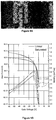
- Figure 4A shows a patterned device prepared according to Example 1 and observed through a polarizing microscope. It can be seen that the areas which have received the increased UV dose show the formation of crystals, whereas the areas which have received the lower UV dosage show no crystal formation and appear black.
- Figure 5A illustrates a non patterned device prepared according to Comparison Example 1 and observed through a polarizing microscope, In this example there is no differentiation between the cross-linking density / UV dosage across the substrate, and hence the formation of crystals occurs over the entire substrate.
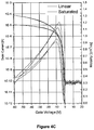
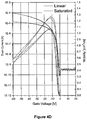
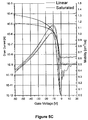
- Figures 4B-D show the typical transistor performance of a patterned device prepared according to Example 1.
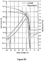
- Figures 5B-D show the typical transistor performance of a non-patterned device prepared according to Comparison Example 1. It can be clearly seen that the off currents measured in the patterned device are lower that that seen in the unpatterened device. This positive effect is seen at no significant detrement to the linear and saturated mobility values, or the value of the on current.
- the bottom gate OFET device in this example is constructed in an identical fashion to that in Example 1, except that the dielectric layer material LisiconTMD203 is substituted by LisiconTMD206 in step b, the UV dose used in step c is UVA (365nm) at a power of 0.01 W/cm 2 for 30 seconds (0.3 J/cm 2 dose), and the UV dose used in step d is UVA (365nm) at a power of 0.01 W/cm 2 for 60 seconds (0.6 J/cm2 dose).
- the UV dose used in step c is UVA (365nm) at a power of 0.01 W/cm 2 for 30 seconds (0.3 J/cm 2 dose)
- the UV dose used in step d is UVA (365nm) at a power of 0.01 W/cm 2 for 60 seconds (0.6 J/cm2 dose).
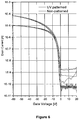
- Figure 6 shows the typical transistor performance of a device prepared by the method described in Example 2 with 365nm UVA radiation, which has been fabricated in such a way to produce both patterned and unpatterened areas (half the substrate was irradiated without the use of a shadow mask). Measurement of the transistor characteristics shows the patterning to have an effect on reducing the off current to the detection limit of the apperatus. The unpatterned device shows a higher, and less stable value for the off current. There is no change in the measured on-current.
- a patterned top gate OFET device is prepared as follows.
- a substrate of Corning 1737 glass is sonicated in 3% Decon90 for 30min at 70°C, washed 2 times with water and sonicated in MeOH, then dried by spin off on the spin coater.
- a dielectric layer of LisiconTMD203 (available from Merck KGaA, Darmstadt, Germany) is spun onto the substrate (1500 rpm for 30 s) and heated on a hotplate for 1 min at 120°C (step aa).
- the entire substrate is exposed to UVB irradiation between 320-390 nm for 30 seconds at a power of 0.1 W/cm 2 (total dose is 3 J/cm 2 ).
- the substrate is then exposed through a shadow mask to a second dose of UVB irradiation between 320-390 nm for 30s at a power of 0.1 W/cm 2 (step bb).
- the areas exposed are those in which crystallisation is required.
- the substrate is treated with the surface treatment formulation LisiconTM M001 (available from Merck KGaA, Darmstadt, Germany) for 1min, washed with isopropyl alcohol and dried by spin off on the spin coater.
- the OSC Formulation LisiconTM S1200 (available from Merck KGaA, Darmstadt, Germany) is spun onto the substrate after the above treatment and then annealed for 1 min at 100°C on a hotplate (step dd).
- a dielectric layer of CYTOPTM (9% in FC-43, Asahi) is spun onto the cooled substrate (500 rpm for 10 s and 2000 rpm for 20 s) and heated on a hotplate for 2 min at 100°C (step ee).
- step ff a 30 nm gold layer is evaporated onto the interlayer as the gate electrode.
- Figure 7 illustrates the greatly improved off-current when a patterned TG device is produced.
- the comparative device is a standard top gate device, prepared on a cleaned glass substrate with no patterning interlayer, onto which the S/D electrodes were thermally evaporated.
Landscapes
- Engineering & Computer Science (AREA)
- Manufacturing & Machinery (AREA)
- Thin Film Transistor (AREA)
- Formation Of Insulating Films (AREA)
Priority Applications (1)
| Application Number | Priority Date | Filing Date | Title |
|---|---|---|---|
| EP11741411.0A EP2612377B1 (en) | 2010-09-02 | 2011-08-05 | Process for preparing an organic electronic device |
Applications Claiming Priority (3)
| Application Number | Priority Date | Filing Date | Title |
|---|---|---|---|
| EP10009116 | 2010-09-02 | ||
| EP11741411.0A EP2612377B1 (en) | 2010-09-02 | 2011-08-05 | Process for preparing an organic electronic device |
| PCT/EP2011/003950 WO2012028244A1 (en) | 2010-09-02 | 2011-08-05 | Process for preparing an organic electronic device |
Publications (2)
| Publication Number | Publication Date |
|---|---|
| EP2612377A1 EP2612377A1 (en) | 2013-07-10 |
| EP2612377B1 true EP2612377B1 (en) | 2019-10-02 |
Family
ID=44629966
Family Applications (1)
| Application Number | Title | Priority Date | Filing Date |
|---|---|---|---|
| EP11741411.0A Active EP2612377B1 (en) | 2010-09-02 | 2011-08-05 | Process for preparing an organic electronic device |
Country Status (6)
| Country | Link |
|---|---|
| US (1) | US8883546B2 (enExample) |
| EP (1) | EP2612377B1 (enExample) |
| JP (1) | JP2013541190A (enExample) |
| KR (1) | KR20130112882A (enExample) |
| TW (1) | TW201228060A (enExample) |
| WO (1) | WO2012028244A1 (enExample) |
Families Citing this family (11)
| Publication number | Priority date | Publication date | Assignee | Title |
|---|---|---|---|---|
| JP5684715B2 (ja) * | 2008-11-24 | 2015-03-18 | ビーエーエスエフ ソシエタス・ヨーロピアBasf Se | 光硬化性ポリマー性誘電体、及びその製造方法、及びその使用方法 |
| WO2015193818A1 (en) * | 2014-06-16 | 2015-12-23 | Sabic Global Technologies B.V. | Crosslinkable polycarbonates for material extrusion additive manufacturing processes |
| JP6505857B2 (ja) * | 2015-09-24 | 2019-04-24 | 富士フイルム株式会社 | 有機薄膜トランジスタおよび有機薄膜トランジスタの製造方法 |
| US10382806B2 (en) * | 2016-11-14 | 2019-08-13 | DISH Technologies L.L.C. | Apparatus, systems and methods for controlling presentation of content using a multi-media table |
| GB2563191A (en) * | 2017-03-15 | 2018-12-12 | Flexenable Ltd | Cross-linked polymers |
| CN110997832B (zh) * | 2017-07-31 | 2023-05-05 | 康宁股份有限公司 | 经由添加有机碱的pvdf-hfp的加速热交联以及使用交联的pvdf-hfp作为otft装置的栅极介电材料 |
| GB201810710D0 (en) * | 2018-06-29 | 2018-08-15 | Smartkem Ltd | Sputter Protective Layer For Organic Electronic Devices |
| CN110838546A (zh) * | 2018-08-17 | 2020-02-25 | 康宁股份有限公司 | 用于有机薄膜晶体管的栅极电介质绝缘体的基于pvdf的聚合物的uv交联 |
| US12360455B2 (en) | 2019-02-08 | 2025-07-15 | Brewer Science, Inc. | Poly(cyanocinnamate)s for structural and optical applications |
| US20220045274A1 (en) * | 2020-08-06 | 2022-02-10 | Facebook Technologies Llc | Ofets having organic semiconductor layer with high carrier mobility and in situ isolation |
| CN113410384B (zh) * | 2021-06-28 | 2023-04-07 | 西南大学 | 一种用于柔性场效应晶体管的聚合物介电层的制备方法 |
Family Cites Families (17)
| Publication number | Priority date | Publication date | Assignee | Title |
|---|---|---|---|---|
| JP3246189B2 (ja) | 1994-06-28 | 2002-01-15 | 株式会社日立製作所 | 半導体表示装置 |
| US6690029B1 (en) | 2001-08-24 | 2004-02-10 | University Of Kentucky Research Foundation | Substituted pentacenes and electronic devices made with substituted pentacenes |
| US7098525B2 (en) * | 2003-05-08 | 2006-08-29 | 3M Innovative Properties Company | Organic polymers, electronic devices, and methods |
| US7279777B2 (en) * | 2003-05-08 | 2007-10-09 | 3M Innovative Properties Company | Organic polymers, laminates, and capacitors |
| GB2403023A (en) | 2003-06-20 | 2004-12-22 | Sharp Kk | Organic light emitting device |
| EP1783781A3 (en) | 2003-11-28 | 2007-10-03 | Merck Patent GmbH | Organic semiconducting layer formulations comprising polyacenes and organic binder polymers |
| KR100592278B1 (ko) * | 2004-06-08 | 2006-06-21 | 삼성에스디아이 주식회사 | 박막 트랜지스터 및 이를 구비한 평판표시장치 |
| GB0424342D0 (en) * | 2004-11-03 | 2004-12-08 | Avecia Ltd | Process and device |
| US20090206328A1 (en) * | 2005-01-05 | 2009-08-20 | Kimihiro Matsukawa | Silicon-Containing Photosensitive Composition, Method for Forming Thin Film Pattern Using Same, Protective Film for Electronic Device, Gate Insulating Film And Thin Film Transistor |
| US7385221B1 (en) | 2005-03-08 | 2008-06-10 | University Of Kentucky Research Foundation | Silylethynylated heteroacenes and electronic devices made therewith |
| JP4349307B2 (ja) * | 2005-03-16 | 2009-10-21 | セイコーエプソン株式会社 | 有機半導体装置の製造方法、有機半導体装置、電子デバイスおよび電子機器 |
| US20060231829A1 (en) * | 2005-04-13 | 2006-10-19 | Xerox Corporation | TFT gate dielectric with crosslinked polymer |
| JP2007150246A (ja) | 2005-11-02 | 2007-06-14 | Ricoh Co Ltd | 有機トランジスタ及び表示装置 |
| JP2007256782A (ja) | 2006-03-24 | 2007-10-04 | Sekisui Chem Co Ltd | シリコン含有感光性組成物、これを用いた薄膜パターンの製造方法、電子機器用保護膜、トランジスタ、カラーフィルタ、有機el素子、ゲート絶縁膜及び薄膜トランジスタ |
| US20080161464A1 (en) * | 2006-06-28 | 2008-07-03 | Marks Tobin J | Crosslinked polymeric dielectric materials and methods of manufacturing and use thereof |
| KR101224723B1 (ko) * | 2006-09-15 | 2013-01-21 | 삼성전자주식회사 | 유기 절연막 조성물, 이를 이용하여 제조된 유기 절연막 및유기 박막 트랜지스터 |
| EP2132213B1 (en) | 2007-03-07 | 2013-05-15 | University of Kentucky Research Foundation | Silylethynylated heteroacenes and electronic devices made therewith |
-
2011
- 2011-08-05 US US13/820,318 patent/US8883546B2/en active Active
- 2011-08-05 EP EP11741411.0A patent/EP2612377B1/en active Active
- 2011-08-05 JP JP2013526338A patent/JP2013541190A/ja active Pending
- 2011-08-05 WO PCT/EP2011/003950 patent/WO2012028244A1/en not_active Ceased
- 2011-08-05 KR KR1020137008504A patent/KR20130112882A/ko not_active Withdrawn
- 2011-09-01 TW TW100131551A patent/TW201228060A/zh unknown
Non-Patent Citations (1)
| Title |
|---|
| None * |
Also Published As
| Publication number | Publication date |
|---|---|
| KR20130112882A (ko) | 2013-10-14 |
| US8883546B2 (en) | 2014-11-11 |
| EP2612377A1 (en) | 2013-07-10 |
| WO2012028244A1 (en) | 2012-03-08 |
| JP2013541190A (ja) | 2013-11-07 |
| US20130153885A1 (en) | 2013-06-20 |
| TW201228060A (en) | 2012-07-01 |
Similar Documents
| Publication | Publication Date | Title |
|---|---|---|
| EP2612377B1 (en) | Process for preparing an organic electronic device | |
| US8637343B2 (en) | Process for preparing an electronic device | |
| US20120153285A1 (en) | Solution processable passivation layers for organic electronic devices | |
| US20130161602A1 (en) | Process for modifying electrodes in an organic electronic device | |
| EP2539949B1 (en) | Electrode treatment process for organic electronic devices | |
| Kitahara et al. | Approaching Trap‐Minimized Polymer Thin‐Film Transistors | |
| JP2011233884A (ja) | 薄膜トランジスタ用誘電性組成物 | |
| TWI464182B (zh) | 薄膜電晶體用閘極絕緣膜形成組成物 | |
| US10164191B2 (en) | Methoxyaryl surface modifier and organic electronic devices comprising such methoxyaryl surface modifier | |
| CN106062982A (zh) | 环胺表面改性剂和包含这样的环胺表面改性剂的有机电子器件 | |
| Charas et al. | Observation of field-effect in a cross-linked polyfluorene semiconductor | |
| Saito et al. | Direct patterning of poly (3-hexylthiophene) and its application to organic field-effect transistor | |
| Ding | Large area vacuum fabrication of organic thin-film transistors | |
| HK1141628B (en) | Process for preparing an electronic device | |
| HK1168687A (en) | Solution processable passivation layers for organic electronic devices |
Legal Events
| Date | Code | Title | Description |
|---|---|---|---|
| PUAI | Public reference made under article 153(3) epc to a published international application that has entered the european phase |
Free format text: ORIGINAL CODE: 0009012 |
|
| 17P | Request for examination filed |
Effective date: 20130115 |
|
| AK | Designated contracting states |
Kind code of ref document: A1 Designated state(s): AL AT BE BG CH CY CZ DE DK EE ES FI FR GB GR HR HU IE IS IT LI LT LU LV MC MK MT NL NO PL PT RO RS SE SI SK SM TR |
|
| DAX | Request for extension of the european patent (deleted) | ||
| STAA | Information on the status of an ep patent application or granted ep patent |
Free format text: STATUS: EXAMINATION IS IN PROGRESS |
|
| 17Q | First examination report despatched |
Effective date: 20180709 |
|
| GRAP | Despatch of communication of intention to grant a patent |
Free format text: ORIGINAL CODE: EPIDOSNIGR1 |
|
| STAA | Information on the status of an ep patent application or granted ep patent |
Free format text: STATUS: GRANT OF PATENT IS INTENDED |
|
| INTG | Intention to grant announced |
Effective date: 20190531 |
|
| GRAS | Grant fee paid |
Free format text: ORIGINAL CODE: EPIDOSNIGR3 |
|
| GRAA | (expected) grant |
Free format text: ORIGINAL CODE: 0009210 |
|
| STAA | Information on the status of an ep patent application or granted ep patent |
Free format text: STATUS: THE PATENT HAS BEEN GRANTED |
|
| AK | Designated contracting states |
Kind code of ref document: B1 Designated state(s): AL AT BE BG CH CY CZ DE DK EE ES FI FR GB GR HR HU IE IS IT LI LT LU LV MC MK MT NL NO PL PT RO RS SE SI SK SM TR |
|
| REG | Reference to a national code |
Ref country code: GB Ref legal event code: FG4D |
|
| REG | Reference to a national code |
Ref country code: CH Ref legal event code: EP Ref country code: AT Ref legal event code: REF Ref document number: 1187169 Country of ref document: AT Kind code of ref document: T Effective date: 20191015 |
|
| REG | Reference to a national code |
Ref country code: DE Ref legal event code: R096 Ref document number: 602011062443 Country of ref document: DE |
|
| REG | Reference to a national code |
Ref country code: IE Ref legal event code: FG4D |
|
| REG | Reference to a national code |
Ref country code: NL Ref legal event code: MP Effective date: 20191002 |
|
| REG | Reference to a national code |
Ref country code: LT Ref legal event code: MG4D |
|
| REG | Reference to a national code |
Ref country code: AT Ref legal event code: MK05 Ref document number: 1187169 Country of ref document: AT Kind code of ref document: T Effective date: 20191002 |
|
| PG25 | Lapsed in a contracting state [announced via postgrant information from national office to epo] |
Ref country code: NO Free format text: LAPSE BECAUSE OF FAILURE TO SUBMIT A TRANSLATION OF THE DESCRIPTION OR TO PAY THE FEE WITHIN THE PRESCRIBED TIME-LIMIT Effective date: 20200102 Ref country code: GR Free format text: LAPSE BECAUSE OF FAILURE TO SUBMIT A TRANSLATION OF THE DESCRIPTION OR TO PAY THE FEE WITHIN THE PRESCRIBED TIME-LIMIT Effective date: 20200103 Ref country code: BG Free format text: LAPSE BECAUSE OF FAILURE TO SUBMIT A TRANSLATION OF THE DESCRIPTION OR TO PAY THE FEE WITHIN THE PRESCRIBED TIME-LIMIT Effective date: 20200102 Ref country code: NL Free format text: LAPSE BECAUSE OF FAILURE TO SUBMIT A TRANSLATION OF THE DESCRIPTION OR TO PAY THE FEE WITHIN THE PRESCRIBED TIME-LIMIT Effective date: 20191002 Ref country code: PL Free format text: LAPSE BECAUSE OF FAILURE TO SUBMIT A TRANSLATION OF THE DESCRIPTION OR TO PAY THE FEE WITHIN THE PRESCRIBED TIME-LIMIT Effective date: 20191002 Ref country code: LT Free format text: LAPSE BECAUSE OF FAILURE TO SUBMIT A TRANSLATION OF THE DESCRIPTION OR TO PAY THE FEE WITHIN THE PRESCRIBED TIME-LIMIT Effective date: 20191002 Ref country code: ES Free format text: LAPSE BECAUSE OF FAILURE TO SUBMIT A TRANSLATION OF THE DESCRIPTION OR TO PAY THE FEE WITHIN THE PRESCRIBED TIME-LIMIT Effective date: 20191002 Ref country code: LV Free format text: LAPSE BECAUSE OF FAILURE TO SUBMIT A TRANSLATION OF THE DESCRIPTION OR TO PAY THE FEE WITHIN THE PRESCRIBED TIME-LIMIT Effective date: 20191002 Ref country code: SE Free format text: LAPSE BECAUSE OF FAILURE TO SUBMIT A TRANSLATION OF THE DESCRIPTION OR TO PAY THE FEE WITHIN THE PRESCRIBED TIME-LIMIT Effective date: 20191002 Ref country code: PT Free format text: LAPSE BECAUSE OF FAILURE TO SUBMIT A TRANSLATION OF THE DESCRIPTION OR TO PAY THE FEE WITHIN THE PRESCRIBED TIME-LIMIT Effective date: 20200203 Ref country code: AT Free format text: LAPSE BECAUSE OF FAILURE TO SUBMIT A TRANSLATION OF THE DESCRIPTION OR TO PAY THE FEE WITHIN THE PRESCRIBED TIME-LIMIT Effective date: 20191002 Ref country code: FI Free format text: LAPSE BECAUSE OF FAILURE TO SUBMIT A TRANSLATION OF THE DESCRIPTION OR TO PAY THE FEE WITHIN THE PRESCRIBED TIME-LIMIT Effective date: 20191002 |
|
| RAP2 | Party data changed (patent owner data changed or rights of a patent transferred) |
Owner name: FLEXENABLE LIMITED |
|
| PG25 | Lapsed in a contracting state [announced via postgrant information from national office to epo] |
Ref country code: IS Free format text: LAPSE BECAUSE OF FAILURE TO SUBMIT A TRANSLATION OF THE DESCRIPTION OR TO PAY THE FEE WITHIN THE PRESCRIBED TIME-LIMIT Effective date: 20200224 Ref country code: CZ Free format text: LAPSE BECAUSE OF FAILURE TO SUBMIT A TRANSLATION OF THE DESCRIPTION OR TO PAY THE FEE WITHIN THE PRESCRIBED TIME-LIMIT Effective date: 20191002 Ref country code: RS Free format text: LAPSE BECAUSE OF FAILURE TO SUBMIT A TRANSLATION OF THE DESCRIPTION OR TO PAY THE FEE WITHIN THE PRESCRIBED TIME-LIMIT Effective date: 20191002 Ref country code: HR Free format text: LAPSE BECAUSE OF FAILURE TO SUBMIT A TRANSLATION OF THE DESCRIPTION OR TO PAY THE FEE WITHIN THE PRESCRIBED TIME-LIMIT Effective date: 20191002 |
|
| PG25 | Lapsed in a contracting state [announced via postgrant information from national office to epo] |
Ref country code: AL Free format text: LAPSE BECAUSE OF FAILURE TO SUBMIT A TRANSLATION OF THE DESCRIPTION OR TO PAY THE FEE WITHIN THE PRESCRIBED TIME-LIMIT Effective date: 20191002 |
|
| REG | Reference to a national code |
Ref country code: DE Ref legal event code: R097 Ref document number: 602011062443 Country of ref document: DE |
|
| PG2D | Information on lapse in contracting state deleted |
Ref country code: IS |
|
| PG25 | Lapsed in a contracting state [announced via postgrant information from national office to epo] |
Ref country code: DK Free format text: LAPSE BECAUSE OF FAILURE TO SUBMIT A TRANSLATION OF THE DESCRIPTION OR TO PAY THE FEE WITHIN THE PRESCRIBED TIME-LIMIT Effective date: 20191002 Ref country code: EE Free format text: LAPSE BECAUSE OF FAILURE TO SUBMIT A TRANSLATION OF THE DESCRIPTION OR TO PAY THE FEE WITHIN THE PRESCRIBED TIME-LIMIT Effective date: 20191002 Ref country code: RO Free format text: LAPSE BECAUSE OF FAILURE TO SUBMIT A TRANSLATION OF THE DESCRIPTION OR TO PAY THE FEE WITHIN THE PRESCRIBED TIME-LIMIT Effective date: 20191002 Ref country code: IS Free format text: LAPSE BECAUSE OF FAILURE TO SUBMIT A TRANSLATION OF THE DESCRIPTION OR TO PAY THE FEE WITHIN THE PRESCRIBED TIME-LIMIT Effective date: 20200202 |
|
| PLBE | No opposition filed within time limit |
Free format text: ORIGINAL CODE: 0009261 |
|
| STAA | Information on the status of an ep patent application or granted ep patent |
Free format text: STATUS: NO OPPOSITION FILED WITHIN TIME LIMIT |
|
| PG25 | Lapsed in a contracting state [announced via postgrant information from national office to epo] |
Ref country code: IT Free format text: LAPSE BECAUSE OF FAILURE TO SUBMIT A TRANSLATION OF THE DESCRIPTION OR TO PAY THE FEE WITHIN THE PRESCRIBED TIME-LIMIT Effective date: 20191002 Ref country code: SK Free format text: LAPSE BECAUSE OF FAILURE TO SUBMIT A TRANSLATION OF THE DESCRIPTION OR TO PAY THE FEE WITHIN THE PRESCRIBED TIME-LIMIT Effective date: 20191002 Ref country code: SM Free format text: LAPSE BECAUSE OF FAILURE TO SUBMIT A TRANSLATION OF THE DESCRIPTION OR TO PAY THE FEE WITHIN THE PRESCRIBED TIME-LIMIT Effective date: 20191002 |
|
| 26N | No opposition filed |
Effective date: 20200703 |
|
| PG25 | Lapsed in a contracting state [announced via postgrant information from national office to epo] |
Ref country code: SI Free format text: LAPSE BECAUSE OF FAILURE TO SUBMIT A TRANSLATION OF THE DESCRIPTION OR TO PAY THE FEE WITHIN THE PRESCRIBED TIME-LIMIT Effective date: 20191002 |
|
| PG25 | Lapsed in a contracting state [announced via postgrant information from national office to epo] |
Ref country code: MC Free format text: LAPSE BECAUSE OF FAILURE TO SUBMIT A TRANSLATION OF THE DESCRIPTION OR TO PAY THE FEE WITHIN THE PRESCRIBED TIME-LIMIT Effective date: 20191002 |
|
| REG | Reference to a national code |
Ref country code: CH Ref legal event code: PL |
|
| PG25 | Lapsed in a contracting state [announced via postgrant information from national office to epo] |
Ref country code: LU Free format text: LAPSE BECAUSE OF NON-PAYMENT OF DUE FEES Effective date: 20200805 Ref country code: LI Free format text: LAPSE BECAUSE OF NON-PAYMENT OF DUE FEES Effective date: 20200831 Ref country code: CH Free format text: LAPSE BECAUSE OF NON-PAYMENT OF DUE FEES Effective date: 20200831 |
|
| REG | Reference to a national code |
Ref country code: BE Ref legal event code: MM Effective date: 20200831 |
|
| PG25 | Lapsed in a contracting state [announced via postgrant information from national office to epo] |
Ref country code: IE Free format text: LAPSE BECAUSE OF NON-PAYMENT OF DUE FEES Effective date: 20200805 Ref country code: BE Free format text: LAPSE BECAUSE OF NON-PAYMENT OF DUE FEES Effective date: 20200831 |
|
| PG25 | Lapsed in a contracting state [announced via postgrant information from national office to epo] |
Ref country code: TR Free format text: LAPSE BECAUSE OF FAILURE TO SUBMIT A TRANSLATION OF THE DESCRIPTION OR TO PAY THE FEE WITHIN THE PRESCRIBED TIME-LIMIT Effective date: 20191002 Ref country code: MT Free format text: LAPSE BECAUSE OF FAILURE TO SUBMIT A TRANSLATION OF THE DESCRIPTION OR TO PAY THE FEE WITHIN THE PRESCRIBED TIME-LIMIT Effective date: 20191002 Ref country code: CY Free format text: LAPSE BECAUSE OF FAILURE TO SUBMIT A TRANSLATION OF THE DESCRIPTION OR TO PAY THE FEE WITHIN THE PRESCRIBED TIME-LIMIT Effective date: 20191002 |
|
| PG25 | Lapsed in a contracting state [announced via postgrant information from national office to epo] |
Ref country code: MK Free format text: LAPSE BECAUSE OF FAILURE TO SUBMIT A TRANSLATION OF THE DESCRIPTION OR TO PAY THE FEE WITHIN THE PRESCRIBED TIME-LIMIT Effective date: 20191002 |
|
| REG | Reference to a national code |
Ref country code: DE Ref legal event code: R079 Ref document number: 602011062443 Country of ref document: DE Free format text: PREVIOUS MAIN CLASS: H01L0051050000 Ipc: H10K0010000000 |
|
| REG | Reference to a national code |
Ref country code: GB Ref legal event code: 732E Free format text: REGISTERED BETWEEN 20230427 AND 20230503 |
|
| P01 | Opt-out of the competence of the unified patent court (upc) registered |
Effective date: 20230528 |
|
| REG | Reference to a national code |
Ref country code: DE Ref legal event code: R081 Ref document number: 602011062443 Country of ref document: DE Owner name: FLEXENABLE TECHNOLOGY LTD., GB Free format text: FORMER OWNER: MERCK PATENT GMBH, 64293 DARMSTADT, DE |
|
| PGFP | Annual fee paid to national office [announced via postgrant information from national office to epo] |
Ref country code: GB Payment date: 20260219 Year of fee payment: 15 |
|
| PGFP | Annual fee paid to national office [announced via postgrant information from national office to epo] |
Ref country code: DE Payment date: 20260219 Year of fee payment: 15 |
|
| PGFP | Annual fee paid to national office [announced via postgrant information from national office to epo] |
Ref country code: FR Payment date: 20260219 Year of fee payment: 15 |