EP2587613A2 - Récepteur de puissance sans fil pour ajuster l'amplitude de puissance sans fil - Google Patents
Récepteur de puissance sans fil pour ajuster l'amplitude de puissance sans fil Download PDFInfo
- Publication number
- EP2587613A2 EP2587613A2 EP12188918.2A EP12188918A EP2587613A2 EP 2587613 A2 EP2587613 A2 EP 2587613A2 EP 12188918 A EP12188918 A EP 12188918A EP 2587613 A2 EP2587613 A2 EP 2587613A2
- Authority
- EP
- European Patent Office
- Prior art keywords
- wireless power
- power
- receiver
- power receiver
- wireless
- Prior art date
- Legal status (The legal status is an assumption and is not a legal conclusion. Google has not performed a legal analysis and makes no representation as to the accuracy of the status listed.)
- Granted
Links
- 238000000034 method Methods 0.000 claims description 19
- 238000004891 communication Methods 0.000 claims description 10
- 238000001914 filtration Methods 0.000 claims description 4
- 230000005669 field effect Effects 0.000 claims description 3
- 239000004065 semiconductor Substances 0.000 claims description 3
- 239000003990 capacitor Substances 0.000 description 56
- 230000005540 biological transmission Effects 0.000 description 8
- 230000001276 controlling effect Effects 0.000 description 8
- 238000010586 diagram Methods 0.000 description 7
- 238000005516 engineering process Methods 0.000 description 5
- 238000012545 processing Methods 0.000 description 5
- 238000009774 resonance method Methods 0.000 description 5
- 230000003247 decreasing effect Effects 0.000 description 4
- 230000005674 electromagnetic induction Effects 0.000 description 3
- 230000008901 benefit Effects 0.000 description 2
- 230000005672 electromagnetic field Effects 0.000 description 2
- 239000011521 glass Substances 0.000 description 2
- 230000006698 induction Effects 0.000 description 2
- 238000010295 mobile communication Methods 0.000 description 2
- 230000009467 reduction Effects 0.000 description 2
- 230000003321 amplification Effects 0.000 description 1
- 230000008859 change Effects 0.000 description 1
- 238000011109 contamination Methods 0.000 description 1
- 238000007796 conventional method Methods 0.000 description 1
- 230000007423 decrease Effects 0.000 description 1
- 230000000694 effects Effects 0.000 description 1
- 230000005611 electricity Effects 0.000 description 1
- 238000002474 experimental method Methods 0.000 description 1
- 238000012986 modification Methods 0.000 description 1
- 230000004048 modification Effects 0.000 description 1
- 238000003199 nucleic acid amplification method Methods 0.000 description 1
- 230000008569 process Effects 0.000 description 1
- 230000005855 radiation Effects 0.000 description 1
- 230000001105 regulatory effect Effects 0.000 description 1
- 230000004044 response Effects 0.000 description 1
Images


Classifications
-
- H—ELECTRICITY
- H02—GENERATION; CONVERSION OR DISTRIBUTION OF ELECTRIC POWER
- H02J—CIRCUIT ARRANGEMENTS OR SYSTEMS FOR SUPPLYING OR DISTRIBUTING ELECTRIC POWER; SYSTEMS FOR STORING ELECTRIC ENERGY
- H02J50/00—Circuit arrangements or systems for wireless supply or distribution of electric power
- H02J50/10—Circuit arrangements or systems for wireless supply or distribution of electric power using inductive coupling
- H02J50/12—Circuit arrangements or systems for wireless supply or distribution of electric power using inductive coupling of the resonant type
-
- H—ELECTRICITY
- H02—GENERATION; CONVERSION OR DISTRIBUTION OF ELECTRIC POWER
- H02J—CIRCUIT ARRANGEMENTS OR SYSTEMS FOR SUPPLYING OR DISTRIBUTING ELECTRIC POWER; SYSTEMS FOR STORING ELECTRIC ENERGY
- H02J50/00—Circuit arrangements or systems for wireless supply or distribution of electric power
- H02J50/10—Circuit arrangements or systems for wireless supply or distribution of electric power using inductive coupling
-
- H—ELECTRICITY
- H02—GENERATION; CONVERSION OR DISTRIBUTION OF ELECTRIC POWER
- H02J—CIRCUIT ARRANGEMENTS OR SYSTEMS FOR SUPPLYING OR DISTRIBUTING ELECTRIC POWER; SYSTEMS FOR STORING ELECTRIC ENERGY
- H02J50/00—Circuit arrangements or systems for wireless supply or distribution of electric power
- H02J50/80—Circuit arrangements or systems for wireless supply or distribution of electric power involving the exchange of data, concerning supply or distribution of electric power, between transmitting devices and receiving devices
-
- H—ELECTRICITY
- H02—GENERATION; CONVERSION OR DISTRIBUTION OF ELECTRIC POWER
- H02J—CIRCUIT ARRANGEMENTS OR SYSTEMS FOR SUPPLYING OR DISTRIBUTING ELECTRIC POWER; SYSTEMS FOR STORING ELECTRIC ENERGY
- H02J50/00—Circuit arrangements or systems for wireless supply or distribution of electric power
- H02J50/90—Circuit arrangements or systems for wireless supply or distribution of electric power involving detection or optimisation of position, e.g. alignment
-
- H—ELECTRICITY
- H02—GENERATION; CONVERSION OR DISTRIBUTION OF ELECTRIC POWER
- H02J—CIRCUIT ARRANGEMENTS OR SYSTEMS FOR SUPPLYING OR DISTRIBUTING ELECTRIC POWER; SYSTEMS FOR STORING ELECTRIC ENERGY
- H02J7/00—Circuit arrangements for charging or depolarising batteries or for supplying loads from batteries
- H02J7/00032—Circuit arrangements for charging or depolarising batteries or for supplying loads from batteries characterised by data exchange
- H02J7/00045—Authentication, i.e. circuits for checking compatibility between one component, e.g. a battery or a battery charger, and another component, e.g. a power source
-
- H—ELECTRICITY
- H02—GENERATION; CONVERSION OR DISTRIBUTION OF ELECTRIC POWER
- H02M—APPARATUS FOR CONVERSION BETWEEN AC AND AC, BETWEEN AC AND DC, OR BETWEEN DC AND DC, AND FOR USE WITH MAINS OR SIMILAR POWER SUPPLY SYSTEMS; CONVERSION OF DC OR AC INPUT POWER INTO SURGE OUTPUT POWER; CONTROL OR REGULATION THEREOF
- H02M7/00—Conversion of ac power input into dc power output; Conversion of dc power input into ac power output
- H02M7/02—Conversion of ac power input into dc power output without possibility of reversal
- H02M7/04—Conversion of ac power input into dc power output without possibility of reversal by static converters
- H02M7/12—Conversion of ac power input into dc power output without possibility of reversal by static converters using discharge tubes with control electrode or semiconductor devices with control electrode
- H02M7/21—Conversion of ac power input into dc power output without possibility of reversal by static converters using discharge tubes with control electrode or semiconductor devices with control electrode using devices of a triode or transistor type requiring continuous application of a control signal
- H02M7/217—Conversion of ac power input into dc power output without possibility of reversal by static converters using discharge tubes with control electrode or semiconductor devices with control electrode using devices of a triode or transistor type requiring continuous application of a control signal using semiconductor devices only
- H02M7/2176—Conversion of ac power input into dc power output without possibility of reversal by static converters using discharge tubes with control electrode or semiconductor devices with control electrode using devices of a triode or transistor type requiring continuous application of a control signal using semiconductor devices only comprising a passive stage to generate a rectified sinusoidal voltage and a controlled switching element in series between such stage and the output
Definitions
- the present invention relates generally to a wireless power receiver, and more particularly, to a wireless power receiver for wirelessly receiving power based on an electromagnetic resonance method.
- Mobile terminals such as cell phones and Personal Digital Assistants (PDAs) are powered by naturally rechargeable batteries, and supply electric energy to the battery using a separate charging device in order to recharge the battery.
- the charging device and the battery are electrically connected by a connection of their outer-surface terminals to each other.
- the contacting terminals are susceptible to contamination by dirt because they extend outward, thus suffering from inappropriate charging, and they may not be properly charged when exposed to moisture.
- the wireless charging technology using wireless power transmission and reception enables, for example, a battery of a cell phone to be automatically charged by placing the cell phone on a charging pad without requiring a separate charging connector.
- This method is currently applied to wireless electric toothbrushes or a wireless electric shaver.
- the electronic device may benefit from enhanced waterproof and portable functions since no wired charging device is required. This technology is expected to be further developed in the burgeoning era of electric vehicles.
- the wireless charging technology has an electromagnetic induction method using coils, a resonance method using resonance, and a Radio Frequency (RF)/micro wave radiation method that converts electric energy into microwaves for transmission.
- RF Radio Frequency
- a power transmission method based on electromagnetic induction is based on transferring power between primary and secondary coils. Moving a magnet through a coil produces an induced current based on which a magnetic field is produced at the transmission end, and the change in the magnetic field at a receiving end induces a current to generate energy. This phenomenon is referred to as magnetic induction, and the power transmission method based on the magnetic induction provides superior energy transmission efficiency.
- Resonant electric energy of the electromagnetic waves is directly transferred only when there is a device having the same resonant frequency and the non-used part of the energy is re-absorbed into the magnetic field rather than being dispersed in the air, and thus the resonant electric energy is not deemed harmful to surrounding machines or bodies.
- a wireless power receiver based on the conventional resonance method includes a rectifier that converts a received Alternating Current (AC) into a Direct Current (DC) and a DC-to-DC converter that adjusts the rectified DC voltage to a voltage preset for an output end.
- AC Alternating Current
- DC Direct Current
- the DC-to-DC converter must use a bulky passive element, it is difficult to implement into the conventional method the wireless power receiver that satisfies both compactness in appearance and high output performance with high efficiency.
- the wireless power receiver is implemented in a mobile communication device such as a cell phone, such difficulty detrimentally affects the current trend of lighter and smaller mobile devices.
- the DC-to-DC converter uses a frequency in a limited range of 2 to 3 MHz since it is an outwardly packaged active device.
- the conventional wireless power receiver suffers from having to include an additional capacitor, such as for impedance matching, and an additional Zener diode for protection of the entire device.
- the present invention provides a wireless power receiver for adjusting the magnitude of received wireless power by using switching.
- a wireless power receiver for wirelessly receiving power from a wireless power supplier including a power receiver for receiving wireless power from the wireless power supplier and storing the wireless power for a first time period, a rectifier connected to the power receiver for rectifying the wireless power, a power adjuster connected to the rectifier and an output end, for adjusting a magnitude of the wireless power by enabling the power receiver to store the wireless power for the first time period and delivering the wireless power to the output end for a second time period, and a controller for determining the first and second time periods.
- a method of controlling a wireless power receiver for wirelessly receiving power from a wireless power supplier including receiving wireless power from the wireless power supplier, rectifying the wireless power, and adjusting a magnitude of the wireless power by preventing the wireless power from being output by disconnecting a path to an output end of the wireless power receiver for a first time period while outputting the wireless power for a second time period.
- FIG. 1A illustrates a wireless power receiver, according to an embodiment of the present invention.
- the wireless power receiver includes a power receiver 110, a rectifier 120, a power adjuster 130, and a controller 140.
- the power receiver 110 receives wireless power supplied by a wireless power supplier.
- the power may be received based on a resonance method, and thus may be implemented using a loop coil with inductance.
- the power receiver 110 receives the wireless power by resonating with an electromagnetic field produced by the wireless power supplier.
- the power receiver 110 is implemented with the loop coil, the inductance of the loop coil is changeable, so the implementation of receiving electromagnetic waves, i.e., the wireless power with various frequencies, may be made.
- a plurality of loop coils may also be used, and the present invention is not limited thereto, but may uses any means to receive the wireless power by resonating with the electromagnetic waves.
- the rectifier 120 rectifies the input power from the power receiver 110.
- the rectifier 120 may be implemented with a well-known means, such as a diode, but is not limited thereto, and may use any means that serves as a rectifying means, such as by full-bridge diodes, which will be discussed below.
- the power adjuster 130 receives and adjusts the magnitude of the wireless power rectified by the rectifier 110.
- the power adjuster 130 adjusts the magnitude of the wireless power by adjusting at least one of voltage and current of the received wireless power. Specifically, the power adjuster 130 may reduce the magnitude of the wireless power by adjusting the voltage of the wireless power.
- the power adjuster 130 is electrically connected to the rectifier 120 and an output end (not shown).
- the power adjuster 130 enables the received power to be stored in the power receiver 110 by disconnecting a path between the rectifier 120 and the output end for a first time period.
- the wireless power circulates in a closed loop and is not delivered to the output end.
- the power receiver 110 may further include a storage area for storing the circulated wireless power for the first time period, which will be discussed below.
- the power adjuster 130 electrically connects the rectifier 120 and the output end for a second time period by being short-circuited, thus having the wireless power delivered to the output end.
- the power adjuster 130 After the second time period, the power adjuster 130 re-stores the received power in the power receiver 110 by disconnecting the path between the rectifier 120 and the output end for the first time period.
- the wireless power may not be delivered to the output end during the first time period while being delivered to the output end during the second time period, which reduces the magnitude of the wireless power to be delivered to the output end by reducing an average voltage of the wireless power.
- This process is illustrated in FIGS. 1B to 1E .
- FIG. 1B illustrates the wireless power input to the power receiver 110, according to an embodiment of the present invention.
- the wireless power is a waveform having a cycle and anamplitude Vdd.
- FIG. 1C is a waveform resulting from rectifying the wireless power having a positive voltage in the rectifier 120, according to an embodiment of the present invention.
- FIG. 1D is a waveform resulting from adjusting the wireless power in the power adjuster 130, according to an embodiment of the present invention.
- the first time period may be 2.5 times greater than a period of the wireless power
- the second time period may be 0.5 times greater than the period of the wireless power.
- the adjusted wireless power is output only for the second time period and not output for the first time period, i.e., 2.5 times the period of the wireless power.
- FIG. 1E is a waveform of output wireless power at the output end, according to the embodiment of an present invention.
- the outputs of the wireless power is connected with each other, as shown in FIG. 1E .
- the magnitude of the average voltage Va may be reduced to a level lower than the amplitude Vdd and an rms value.
- the magnitude of voltage of the rectified wireless power output by the power adjuster 130 may be decreased compared to that of the originally received wireless power.
- the controller 140 determines the first and second periods. As discussed above in connection with FIGS. 1B through IE, the longer the first time period is, the less the magnitude of the output wireless power becomes because the wireless power circulates longer in the closed loop. In this manner, the magnitude of the output voltage may further be decreased. Conversely, if the controller 140 reduces the first time period, the wireless power circulates less in the closed loop and thus the magnitude of the output wireless power increases. The controller adjusts the magnitude of the output rectified wireless power by controlling the first and second time periods.
- the controller 140 controls general operations of the wireless power receiver, and be implemented with a microprocessor, a Central Processing Unit (CPU), or a mini computer, for example.
- CPU Central Processing Unit
- FIG. 2 illustrates the wireless power receiver, according to another embodiment of the present invention.
- the wireless power receiver 200 includes a power receiver 210, a rectifier 220, a power adjuster 230, a regulator, a feedback circuit 250, a controller 260, a sync detector 270, and a communication unit. Explanation of some overlapping components of the wireless power receiver 200 with the ones in FIG. 1A will be briefly mentioned or skipped, for purposes of conciseness.
- the power receiver 210 includes a receiver 211 and a power storage 212.
- the receiver 211 receives the wireless power by resonating with an electromagnetic field produced by the wireless power supplier.
- the inductance L of the loop coil is changeable, so an implementation of receiving electromagnetic waves, i.e., the wireless power with various frequencies, may be made.
- the power storage 212 stores the power for the first time period.
- the power storage 212 may store the power if the power adjuster 230 is disconnected from the output end (not shown), and be implemented with a capacitor.
- the power adjuster 230 Under control of the controller 260, the power adjuster 230 is open-circuited for the first time period, thus disconnecting the rectifier 220 from the output end, and enables the wireless power to be stored in the power storage 212.
- the power adjuster 230 delivers the wireless power to the output end by being short-circuited for the second time period by using a switch, which may be a load switch.
- the power adjuster 230 will be described below in more detail.
- the power adjuster 230 may be implemented with an N-type Metal-Oxide-Semiconductor Field-Effect Transistor (MOSFET).
- MOSFET Metal-Oxide-Semiconductor Field-Effect Transistor
- the power adjuster 230 may further include a bootstrapper for bootstrapping the power to be applied to the gate of the N-type MOSFET, which will be described below in detail.
- the N-type MOSFET receives a control signal of the controller 260 as a gate input signal, according to which the N-type MOSFET may be open-circuited for the first time period and short-circuited for the second time period.
- the wireless power may be stored in the power storage 212.
- the regulator 240 generates an output wireless power by filtering ripples of the rectified wireless power input by the power adjuster 230.
- the regulator 240 may be implemented with an LC filter, and may thus compensate the rectified wireless power to closer resemble a DC form.
- the regulator 240 may also control the output of the wireless power in order not to be overflowed at the output end.
- the wireless power output by the regulator 240 is output to the outside to be applied to a load or to be stored in a reservoir (not shown) such as a battery.
- the feedback circuit 250 sends the regulated wireless power output by the regulator 240 back to the controller 260 as a feedback wireless power.
- the feedback circuit 250 may be implemented with a wire and a resistance to pass through the current by decreasing the voltage.
- the controller 260 controls general operations of the wireless power receiver 200, and determines the first and second time periods. As described above in connection with FIGS. 1B to 1E , the magnitude of the rectified wireless power output by the power adjuster 230 may be changed according to the duration of the first or second time period determined by the controller 260.
- the output voltage finally output by the regulator 240 requires a voltage value used by the wireless power receiver 200 or a load having the wireless power receiver 200. Thus, the output voltage has to maintain a constant value, and if the value of the output voltage increases or decreases compared with the voltage value, the controller 260 controls the voltage to maintain the voltage value.
- the controller 260 compares the value of the voltage of the feedback wireless power input by the feedback circuit unit 250 with the voltage value.
- the controller 260 includes a well-known comparator such as an OPerational AMPlifier (OP-AMP), which compares the feedback wireless power with the voltage value.
- OP-AMP OPerational AMPlifier
- the controller 260 determines the first and second time periods based on the comparison result. For example, the controller 260 may reduce the output voltage by increasing the duration of the first time period if the comparison result indicates that the output voltage is greater than the voltage value. On the contrary, the controller 260 may increase the output voltage by increasing the duration of the second time period if the comparison result shows that the output voltage is less than the voltage value. In this manner, the wireless power receiver 200 may output the constant voltage, such as 5 V.
- the controller 260 generates a power adjustment signal to control the power adjuster 230 during the first and second time periods and outputs the power adjustment signal to the power adjuster 230.
- the controller 260 generates and applies an application voltage to the gate of the N-type MOSFET.
- the sync detector 270 may detect a sync signal from the wireless power from the power receiver 210.
- the sync signal includes information, such as a period of the wireless power received from the power receiver 210, and output the sync signal detected by the sync detector 270 to the controller 260.
- the controller 260 generates the power adjustment signal based on the sync signal. For example, the controller 260 receives the sync signal informing that the wireless power has a 2.78 MHz frequency, generate a 2. 78 MHz clock, and generates and output a power control signal having a zero value for the first time period of the clock.
- the communication unit 280 communicates with the wireless power supplier based on a communication method.
- the controller 260 generates and outputs to the communication unit 280 the wireless power control signal to control the supplied wireless power based on the feedback wireless power.
- the communication unit 280 transmits the input wireless power control signal to the wireless communication supplier, which may in turn control the wireless power to be supplied based on the wireless power control signal.
- the wireless power control signal includes at least one of identification information of the wireless power receiver, information regarding wireless reception, position information, environment setting information, safety-related information, and control information for the wireless power supplier.
- the control information for the wireless power supplier includes at least one of control information of an application voltage of the wireless power supplier, and control information of frequency and duty cycle of a power supply signal.
- the wireless power supplier changes the magnitude or efficiency of the wireless power for supply by changing the application voltage of the wireless power supplier, the frequency or duty cycle of the power supply signal based on the input wireless power control signal.
- the controller 260 generates the wireless power control signal to request power reduction if the output voltage is greater than the voltage value based on the comparison result, and controls the communication unit 280 to transmit the wireless power control signal.
- the wireless power supplier may reduce the power for supply, such as by reducing the application voltage of the wireless power supplier.
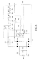
- FIG. 3 is a circuit diagram of the wireless power receiver, according to an embodiment of the present invention.
- the wireless power receiver includes a power receiver 301implemented with a coil.
- the power receiver 301 has one end connected to an end of a capacitor 302, and the other end of the capacitor 302 is connected to a node 303.
- a capacitor 304 capable of storing the power for the first time period has one end connected to the node 303 while having the other end connected to a node 305.
- the node 305 is connected to the other end of the power receiver 301.
- the rectifier includes full-bridge diodes, which are four diodes 306, 307, 308, and 309 as shown in FIG. 3 .
- One end of the diode 306 is connected to the node 303, and the other end is connected to an end of the diode 307 and a power adjuster 311.
- the one end of the diode 306 is also connected to an end of the diode 308, and the other end of the diode 308 is connected to the ground and an end of the diode 309.
- the other end of the diode 309 is connected to the other end of the diode 307 and the node 305.
- a capacitor 310 has an end connected to the diodes 306 and 307, and the power adjuster 311. The other end of the capacitor 310 is grounded.
- the power adjuster 311 is connected to a respective end of each of the diodes 306 and 307, and a capacitor 310, and the other end is connected to a node 312.
- the power adjuster 311 may be a load switch, which may be open-circuited for the first time period and short-circuited for the second time period, as described above.
- the node 312 is connected to the power adjuster 311, a capacitor 313, and an output end.
- the power having 5V voltage, for example, is output at the output end.
- FIG. 4 is a circuit diagram of the wireless power receiver, according to another embodiment of the present invention.
- the wireless power receiver includes a power receiver 401.
- the power receiver 401 may be implemented with a coil.
- the power receiver 401 has one end connected to an end of a capacitor 402.
- the other end of the capacitor 402 is connected to a node 403.
- a capacitor 404 capable of storing the power for the first time period has one end connected to the node 403 while having the other end connected to a node 405.
- the node 405 is connected to the other end of the power receiver 401.
- the rectifier includes full-bridge diodes, which are four diodes 406, 407, 408, and 409 as shown in FIG. 4 .
- One end of the diode 406 is connected to the node 403, and the other end is connected to an end of the diode 407 and a power adjuster 415.
- the one end of the diode 406 may also be connected to an end of the diode 408, and the other end of the diode 408 is connected to the ground and an end of the diode 409.
- the other end of the diode 409 is connected to the other end of the diode 407 and the node 405.
- the diodes 406 and 407 are connected to a bootstrapper 410 and the power adjuster 415, which may be an N-type MOSFET device and further includes the bootstrapper 410 for bootstrapping the voltage to be applied to the gate of the N-type MOSFET device.
- the diodes 406 and 407 are connected to the source of the N-type MOSFET device.
- the bootstrapper 410 bootstraps the voltage to be applied to the gate of the N-type MOSFET device.
- the bootstrapper 410 is implemented with a diode, which is connected to a low signal switch 411 and a low signal capacitor 413.
- the wireless power receiver of FIG. 4 includes two capacitors 413 and 414 and two switches 411 and 412, which are alternately open-circuited and short-circuited in response to high and low signals. Signals are applied in a more reliable fashion with the use of the switches 411 and 412.
- the low signal switch 411 has one end connected to the bootstrapper 410 and the low signal capacitor 413, and the other end to the high signal switch 412 and the high signal capacitor 414.
- the high signal switch is connected to an end of a coil 416, the other end of which is connected to the power adjuster 415, i.e., the gate of the N-type MOSFET device.
- the drain of the power adjuster 415 is connected to an output end 418, which is connected to a capacitor 417.
- FIG. 5 is a circuit diagram of the wireless power receiver, according to another embodiment of the present invention.
- the wireless power receiver includes a wireless power transmitter 501, and electromagnetic waves which radiate from the wireless power transmitter 501 are absorbed by the wireless power receiver 502.
- the wireless power receiver includes a power receiver 502, which is implemented with a coil.
- the power receiver 502 has one end connected to a node 503.
- the node 503 is connected to an end of a capacitor 504.
- the other end of the capacitor 504 is connected to a node 505.
- the node 505 is connected to a rectifier 507 and a capacitor 506.
- the rectifier 507 is connected to a capacitor 508 in parallel, and to a power adjuster 509.
- the power adjuster 509 is connected to an end of a regulator 510 that has a coil and a capacitor. An output of the regulator 510 is connected to an output end 511.
- the regulator 510 generates an output wireless power by filtering out ripples of the rectified wireless power input by the power adjuster 509.
- the regulator 510 may be implemented with an inductor/capacitor (LC) filter, and may thus compensate the rectified wireless power to closer resemble a DC form.
- the regulator 510 may also control the output of the wireless power so that the wireless power does not overflow at the output end.
- the wireless power output by the regulator 510 is output to the outside to be applied to a load or to be stored in a reservoir (not shown) such as a battery.
- the output end 511 is connected to a node 513 through a resistor 512.
- the resistor 512 causes a voltage drop and the output voltage may be returned.
- the controller includes a comparator 515 and a processing unit 516.
- the comparator 515 may be implemented with an OP-AMP, having a first input connected to a node 513 and second input to a voltage Vref. An output of the comparator 515 is connected to the processing unit 516.
- the processing unit 516 is connected to a sync detector 517, and output to the gate of N-type MOSFET 509 the power adjustment signal generated in the above-described manner.
- the sync detector 517 is connected to the other end of the power receiver 502, and outputs a detected sync signal to the processing unit 516.
- FIG. 6 is a circuit diagram of the wireless power receiver, according to another embodiment of the present invention.
- the wireless power receiver includes a power receiver 601, which is implemented with a coil.
- the power receiver 601 has one end connected to an end of a capacitor 602.
- the other end of the capacitor 602 is connected to a capacitor 603 and an end of a diode 605.
- the rectifier includes full-bridge diodes, which are four diodes 605, 606, 607, and 608 as shown in FIG. 6 .
- An end of the diode 605 is connected to a respective end of each of the capacitor 602, the capacitor 603, and the diode 607, and the other end of the diode 605 is connected to an end of the diode 606, a resistor 609, and a capacitor 610.
- the diodes 605 and 606 are connected to a diode 627 and a power adjuster 628.
- the power adjuster 628 may be an N-type MOSFET device and has a bootstrapper for bootstrapping a voltage applied to the gate of the N-type MOSFET device.
- the bootstrapper includes a plurality of MOSFET devices 621, 622, 623, 624, 625, and 626, and a diode 627.
- a MOSFET device 629 connected to the diode 627 and a node 630 senses ripple forms to generate a control signal for the gate of the MOSFET device 628 to be open-circuited or short-circuited.
- a voltage at the node 630 is different from a voltage at the other end of the resistor 609 by Vgs and has a bootstrapped voltage applied.
- the MOSFET device 629 is connected to an end of a capacitor 633, the other end of which is grounded.
- the node 630 is connected to an end of a low signal switch 631, the other end of which is connected to the gate of the power adjuster 628 and an end of a high signal switch 632.
- the other end of the high signal switch 632 is connected to an output end connected to an end of a capacitor 634.
- the other end of the capacitor 634 isgrounded.
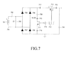
- FIG. 7 is a circuit diagram of the wireless power receiver, according to another embodiment of the present invention.
- the wireless power receiver includes a power receiver 701, which is implemented with a coil.
- the power receiver 701 has one end connected to an end of a capacitor 702.
- the other end of the capacitor 702 is connected to a capacitor 703 and an end of a diode 705.
- the rectifier includes full-bridge diodes, which are four diodes 705, 706, 707, and 708 as shown in FIG. 7 .
- One end of the diode 705 is connected to the capacitor 703, and the other end is connected to an end of the diode 706 and a node 711.
- the node 711 is connected to a power adjuster 712 and an end of a capacitor 709.
- the power adjuster 712 is a P-type MOSFET device and, as opposed to that of FIG. 6 , does not include any bootstrapper.
- the other end of the capacitor 709 is connected to a node 710 possibly having a voltage decreased from a voltage at the node 711 by 5V.
- the node 710 is connected to the source of the MOSFET device 717.
- the gate of the MOSFET device 717 is connected to an inverter 716 outputting a signal 715 in a certain waveform.
- the signal 715 inputs to the gate of the power adjuster 712 to control the power adjuster 712 to be open-circuited or short-circuited.
- the drain of the MOSFET device 717 is connected to a node 718, which is grounded.
- the source of the power adjuster 712 is connected to an output end 713, which is connected to an end of a capacitor 714.
- the other end of the capacitor 714 is grounded.
- FIG. 8 is a circuit diagram of the wireless power receiver, according to another embodiment of the present invention.
- the wireless power receiver of FIG. 8 includes a power receiver 805 having a front end connected to diodes 801 and 802, and a capacitor 803. An end of the diode 802 is grounded and the other end is connected to a delay unit 839, the diode 801, and an end of the capacitor 803. The other end of the capacitor 803 is connected to an end of a capacitor 804 and the power receiver 805.
- the other end of the capacitor 804 is connected to an end of a capacitor 806 and full-bridge diodes 808, 809, 810, and 811.
- An end of a capacitor 806 is connected to the full-bridge diodes 808, 809, 810, and 811 and a node 807 connected to the power receiver 805.
- the full-bridge diodes 808, 809, 810, and 811 are connected to an end of a resistor 812 and an end of a capacitor 813.
- the other ends of the resistor 812 and the capacitor 813 are connected to a node 814, which is connected to the gate of a MOSFET device 816.
- the source of the MOSFET 816 is connected to a bootstrapper 815, and the drain of the MOSFET 816 to a node 821.
- the node 821 is connected to an end of a capacitor 817, the other end of which is grounded.
- the full-bridge diodes 808, 809, 810, and 811 are connected to the bootstrapper 815 and to the source of a power adjuster 818.
- the drain of the power adjuster 818 is connected to an output end 819.
- the output end 819 is connected to an end of a capacitor 820 and an end of a resistor 822.
- An end of the resistor 822 is connected to a node 823, which is connected to an end of a resistor 824.
- the other ends of the capacitor 820 and the resistor 824 are grounded.
- the node 823 is connected to a positive input of a multiplexer 825, and a negative input of the multiplexer 825 has, for example,. -1.2 V voltage applied thereto.
- An output of the multiplexer 825 is connected to a node 826 and a positive input of a comparator 830.
- a negative input of the comparator 830 has a reference voltage applied thereto in a particular waveform, such as a saw waveform.
- An output of the comparator 830 is connected to a D-flipflop 838.
- the node 826 is connected to an end of a resistor 827 and an end of a capacitor 829.
- the other end of the resistor 827 is connected to an end of a capacitor 828, and the other end of the capacitor 828 may be grounded.
- the D-flipflop 838 is connected to the comparator 830 and the delay, as described above.
- the D-flipflop 838 is also connected to a level shifter 837, which is, in turn, connected to a gate driver 836.
- the gate driver 836 divides an input into two outputs, each of which are input to an AND device or an OR device.
- the other ends of the AND and OR devices are connected to the gates of MOSFET devices 834 and 835, respectively.
- Outputs of the AND and OR devices are also connected to the gates of MOSFET devices 834 and 835, respectively.
- a bootstrapped voltage is applied to the source 834 of the MOSFET device 834 and an output voltage is applied to the drain 833 of the MOSFET device 835.
- the drain of the MOSFET device 834 and the source of the MOSFET device 835 are connected together to the gate of the power adjuster 818, and thus the output of the MOSFET devices 834 and 835 is the control signal for the gate of the power adjuster 818.
- control signal for the gate of the power adjuster 818 is produced by a series of the comparator 830 and the error amplification part (838, 837, 836, 834, and 835), which defines a feedback loop.
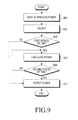
- FIG. 9 illustrates a method of controlling the wireless power receiver, according to an embodiment of the present invention.
- the wireless power receiver receives the wireless power from the wireless power supplier, in step S901. Since the manner of receiving the wireless power has been described above, the explanation will be omitted here.
- the wireless power receiver rectifies a received current, in step S903.
- the wireless power receiver controls the wireless power to circulate in the wireless power receiver by disconnecting the path to the output end of the wireless power receiver during the first time period, in step S907.
- the wireless power receiver may also output a rectified wireless power during the second time period, in step S911.
- the method of controlling the wireless power receiver may further include sending back the rectified wireless power as a feedback wireless power and analyzing the feedback wireless power, in which case the first and second time periods may be determined based on the feedback wireless power.
- the first and second time periods may be determined based on comparison between a voltage of the feedback wireless power and a reference voltage, and the wireless power receiver controls its operations during the first and second time periods by generating the power adjustment signal to control the wireless power receiver for each of the first and second time periods.
- the method of controlling the wireless power receiver may further include a step of detecting a sync signal to be in phase with the power adjustment signal from the received wireless power, in which case the power adjustment signal may be generated based on the sync signal.
- the power adjustment signal may be generated and output by generating a wireless power control signal to control the wireless power based on the feedback wireless power, in which case the method of controlling the wireless power receiver may further include a step of transmitting the wireless power control signal to the wireless power supplier.
- the wireless power control signal includes at least one of identification information of the wireless power receiver, information regarding wireless reception, position information, environment setting information, safety-related information, and control information for the wireless power supplier, and particularly, the control information for the wireless power supplier includes at least one of control information of an application voltage of the wireless power supplier, control information of the frequency of a power supply signal, and control information of the duty cycle of the power supply signal.
- the method of controlling the wireless power receiver may further include generating an output wireless power by filtering out ripples of the rectified wireless power.
- the wireless power receiver adjusts the magnitude of the received wireless power by periodically open-circuiting and short-circuiting of a switch.
- the resonant inductor and capacitor facilitates the achievement of a more reliable DC current.
Landscapes
- Engineering & Computer Science (AREA)
- Power Engineering (AREA)
- Computer Networks & Wireless Communication (AREA)
- Charge And Discharge Circuits For Batteries Or The Like (AREA)
- Rectifiers (AREA)
- Circuits Of Receivers In General (AREA)
- Selective Calling Equipment (AREA)
Applications Claiming Priority (1)
| Application Number | Priority Date | Filing Date | Title |
|---|---|---|---|
| KR1020110107179A KR101933462B1 (ko) | 2011-10-19 | 2011-10-19 | 무선 전력의 크기를 조정하는 무선 전력 수신기 |
Publications (3)
| Publication Number | Publication Date |
|---|---|
| EP2587613A2 true EP2587613A2 (fr) | 2013-05-01 |
| EP2587613A3 EP2587613A3 (fr) | 2017-10-25 |
| EP2587613B1 EP2587613B1 (fr) | 2021-04-07 |
Family
ID=47522241
Family Applications (1)
| Application Number | Title | Priority Date | Filing Date |
|---|---|---|---|
| EP12188918.2A Active EP2587613B1 (fr) | 2011-10-19 | 2012-10-18 | Récepteur de puissance sans fil pour ajuster l'amplitude de puissance sans fil |
Country Status (3)
| Country | Link |
|---|---|
| US (1) | US10069340B2 (fr) |
| EP (1) | EP2587613B1 (fr) |
| KR (1) | KR101933462B1 (fr) |
Cited By (2)
| Publication number | Priority date | Publication date | Assignee | Title |
|---|---|---|---|---|
| CN105896511A (zh) * | 2016-06-28 | 2016-08-24 | 常俊苹 | 一种配电网电磁互感器铁磁谐振过压保护装置 |
| WO2023041229A1 (fr) * | 2021-09-14 | 2023-03-23 | Sew-Eurodrive Gmbh & Co. Kg | Système de transmission d'énergie sans contact d'un conducteur primaire à une partie mobile |
Families Citing this family (29)
| Publication number | Priority date | Publication date | Assignee | Title |
|---|---|---|---|---|
| KR101896921B1 (ko) * | 2011-05-17 | 2018-09-12 | 삼성전자주식회사 | 무선 전력 수신기 및 그 제어 방법 |
| JP5449504B1 (ja) * | 2012-10-31 | 2014-03-19 | 三菱電機エンジニアリング株式会社 | 無線電力伝送による多重化伝送システム及び送信側多重化伝送装置 |
| CN103746462B (zh) * | 2013-07-11 | 2016-01-20 | 重庆米亚车辆技术有限公司 | 一种用于无线电能传输的双边lcc补偿网络及其调谐方法 |
| US9484906B2 (en) | 2013-10-09 | 2016-11-01 | Active-Semi, Inc. | Apparatus and methods of N-type load switch using bootstrap gate drive for wireless power receiver |
| KR102161826B1 (ko) | 2013-11-13 | 2020-10-06 | 삼성전자주식회사 | 전압 컨버터, 이를 포함하는 무선 전력 수신 장치 및 무선 전력 전송 시스템 |
| US9680309B2 (en) | 2013-11-21 | 2017-06-13 | Active-Semi, Inc. | Auto load switch detection for wireless power receiver |
| WO2015093990A1 (fr) * | 2013-12-20 | 2015-06-25 | Auckland Uniservices Limited | Circuit de détection de transfert de puissance inductif comportant un doubleur de courant de sortie |
| US9815379B2 (en) * | 2014-01-21 | 2017-11-14 | Qualcomm Incorporated | Systems and methods for electric vehicle induction coil alignment |
| US9608465B2 (en) | 2014-04-18 | 2017-03-28 | Qualcomm Incorporated | Devices, systems, and method for power control of dynamic electric vehicle charging systems |
| US9635222B2 (en) | 2014-08-03 | 2017-04-25 | PogoTec, Inc. | Wearable camera systems and apparatus for aligning an eyewear camera |
| CN106687858A (zh) | 2014-08-03 | 2017-05-17 | 波戈技术有限公司 | 可穿戴相机系统与用于将相机系统或其它电子装置附接到可穿戴物品的设备及方法 |
| TW201724837A (zh) | 2014-12-23 | 2017-07-01 | 帕戈技術股份有限公司 | 穿戴式相機、用於提供無線電力之系統,用於以無線方式提供電力之方法及用於處理影像之方法 |
| KR101579898B1 (ko) * | 2015-01-23 | 2015-12-28 | 한국과학기술원 | 다중 안테나 송신장치 및 수신 장치 |
| AU2016274951A1 (en) | 2015-06-10 | 2018-01-04 | PogoTec, Inc. | Eyewear with magnetic track for electronic wearable device |
| US10481417B2 (en) | 2015-06-10 | 2019-11-19 | PogoTec, Inc. | Magnetic attachment mechanism for electronic wearable device |
| TW201729610A (zh) | 2015-10-29 | 2017-08-16 | 帕戈技術股份有限公司 | 適用於無線功率接收之助聽器 |
| US11558538B2 (en) | 2016-03-18 | 2023-01-17 | Opkix, Inc. | Portable camera system |
| KR102620940B1 (ko) * | 2016-05-30 | 2024-01-05 | 주식회사 위츠 | 무선전력수신장치 |
| EP3539285A4 (fr) | 2016-11-08 | 2020-09-02 | Pogotec, Inc. | Boîtier intelligent de dispositif électronique portatif |
| US10931149B2 (en) | 2018-06-29 | 2021-02-23 | Etherdyne Technologies, Inc. | Wireless power receiver circuits that provide constant voltage or current to an electrical load, and methods |
| US11362543B2 (en) | 2018-06-29 | 2022-06-14 | Etherdyne Technologies, Inc. | Wireless power receiver circuits that provide constant voltage or current to an electrical load, and methods |
| US11300857B2 (en) | 2018-11-13 | 2022-04-12 | Opkix, Inc. | Wearable mounts for portable camera |
| WO2020144623A1 (fr) | 2019-01-10 | 2020-07-16 | Powermat Technologies Ltd | Régulateur de tension à faible perte pour récepteurs de charge sans fil |
| JP7271256B2 (ja) * | 2019-03-28 | 2023-05-11 | ラピスセミコンダクタ株式会社 | 受電装置 |
| TWI744659B (zh) * | 2019-07-01 | 2021-11-01 | 美商艾勒迪科技股份有限公司 | 提供恆定電壓或電流至電力負載之無線電力接收器電路及其方法 |
| KR102233919B1 (ko) * | 2019-07-18 | 2021-03-29 | 숙명여자대학교산학협력단 | 데이터를 송수신하는 무선 전력 송신 장치, 무선 전력 수신 장치, 및 무선 전력 전달 시스템 |
| US11368038B2 (en) * | 2019-08-06 | 2022-06-21 | Microsoft Technology Licensing, Llc | Adaptive wireless charging receiver loading |
| US11431201B2 (en) | 2019-09-16 | 2022-08-30 | Analog Devices International Unlimited Company | Techniques for improved wireless energy transmission efficiency |
| WO2022102481A1 (fr) * | 2020-11-16 | 2022-05-19 | 株式会社村田製作所 | Système de circuit de réception d'énergie sans fil |
Family Cites Families (16)
| Publication number | Priority date | Publication date | Assignee | Title |
|---|---|---|---|---|
| JP2952897B2 (ja) * | 1989-07-28 | 1999-09-27 | 株式会社安川電機 | ゲート駆動回路 |
| US6879809B1 (en) * | 1998-04-16 | 2005-04-12 | Motorola, Inc. | Wireless electrostatic charging and communicating system |
| DE29816725U1 (de) * | 1998-09-17 | 1999-01-14 | Chao, Wen-Chung, Yungho, Taipeh | Ladungsvorrichtung für mobile Telefone |
| AU2000260170A1 (en) * | 2000-07-14 | 2002-01-30 | Yamatake Corporation | Electromagnetically coupled device |
| US7233137B2 (en) * | 2003-09-30 | 2007-06-19 | Sharp Kabushiki Kaisha | Power supply system |
| GB2414120B (en) | 2004-05-11 | 2008-04-02 | Splashpower Ltd | Controlling inductive power transfer systems |
| TWI339471B (en) | 2006-12-27 | 2011-03-21 | Ind Tech Res Inst | Non-contact power supply having built-in coupling detection device and coupling detection method thereof |
| US20090160261A1 (en) | 2007-12-19 | 2009-06-25 | Nokia Corporation | Wireless energy transfer |
| CA2711489A1 (fr) | 2008-01-07 | 2009-07-16 | David W. Baarman | Alimentation electrique inductrice avec commande de cycle de marche |
| JP5297104B2 (ja) * | 2008-07-01 | 2013-09-25 | ルネサスエレクトロニクス株式会社 | 半導体装置 |
| US8338991B2 (en) * | 2009-03-20 | 2012-12-25 | Qualcomm Incorporated | Adaptive impedance tuning in wireless power transmission |
| JP5460138B2 (ja) * | 2009-06-23 | 2014-04-02 | キヤノン株式会社 | スイッチング素子の駆動回路、コンバータ |
| US8547057B2 (en) | 2009-11-17 | 2013-10-01 | Qualcomm Incorporated | Systems and methods for selective wireless power transfer |
| US9570985B2 (en) * | 2010-07-02 | 2017-02-14 | Renesas Electronics America Inc. | Intelligent gate drive voltage generator |
| US9219378B2 (en) * | 2010-11-01 | 2015-12-22 | Qualcomm Incorporated | Wireless charging of devices |
| US9337664B2 (en) * | 2010-12-16 | 2016-05-10 | Qualcomm Incorporated | Wireless power receiver circuitry |
-
2011
- 2011-10-19 KR KR1020110107179A patent/KR101933462B1/ko active IP Right Grant
-
2012
- 2012-10-18 EP EP12188918.2A patent/EP2587613B1/fr active Active
- 2012-10-19 US US13/656,142 patent/US10069340B2/en active Active
Non-Patent Citations (1)
| Title |
|---|
| None |
Cited By (2)
| Publication number | Priority date | Publication date | Assignee | Title |
|---|---|---|---|---|
| CN105896511A (zh) * | 2016-06-28 | 2016-08-24 | 常俊苹 | 一种配电网电磁互感器铁磁谐振过压保护装置 |
| WO2023041229A1 (fr) * | 2021-09-14 | 2023-03-23 | Sew-Eurodrive Gmbh & Co. Kg | Système de transmission d'énergie sans contact d'un conducteur primaire à une partie mobile |
Also Published As
| Publication number | Publication date |
|---|---|
| KR101933462B1 (ko) | 2019-01-02 |
| EP2587613A3 (fr) | 2017-10-25 |
| US20130099588A1 (en) | 2013-04-25 |
| EP2587613B1 (fr) | 2021-04-07 |
| US10069340B2 (en) | 2018-09-04 |
| KR20130042992A (ko) | 2013-04-29 |
Similar Documents
| Publication | Publication Date | Title |
|---|---|---|
| US10069340B2 (en) | Wireless power receiver for adjusting magnitude of wireless power | |
| US11043856B2 (en) | Wireless power receiver and controlling method thereof | |
| KR101893104B1 (ko) | 스위치를 이용하여 무선 전력을 조정하는 무선 전력 수신기 | |
| US20230178817A1 (en) | Feed unit, feed system, and electronic device for increasing power supplied to a battery based on a device state and/or a control of a charging current | |
| JP6070789B2 (ja) | 給電装置および給電システム | |
| US9641019B2 (en) | Wireless power transmitter and method of controlling the same | |
| KR102042685B1 (ko) | 무선 전력 전송 장치 및 무선 전력 수신 장치 | |
| US9425629B2 (en) | Wireless power receiver | |
| US8111041B2 (en) | Power transmission control device, power reception control device, non-contact power transmission system, power transmission device, power reception device, and electronic instrument | |
| US9270124B2 (en) | Contactless power supply device | |
| KR20130035205A (ko) | 수전 장치 및 비접촉 급전 시스템 | |
| US9438062B2 (en) | Wireless electric power receiver for wirelessly regulating electric power using switch | |
| US20160308393A1 (en) | Contactless power receiver and method for operating same | |
| CN107681717B (zh) | 电子设备 | |
| KR101712647B1 (ko) | 무선 충방전 보조 배터리 | |
| KR20170047768A (ko) | 고효율 무선 전력 전송을 위한 부하 전류에 따른 정류 전압 가변 방법 | |
| KR20130123082A (ko) | 무선 전력 송신기 및 무선 전력 수신기 | |
| KR20170065910A (ko) | 무선 전력 송신 장치 | |
| KR20170047707A (ko) | 고효율 무선전력 전송을 위한 고정임피던스 수신기기 전력 시스템 및 충전 방법 | |
| JP2016082782A (ja) | ワイヤレス受電装置 |
Legal Events
| Date | Code | Title | Description |
|---|---|---|---|
| PUAI | Public reference made under article 153(3) epc to a published international application that has entered the european phase |
Free format text: ORIGINAL CODE: 0009012 |
|
| AK | Designated contracting states |
Kind code of ref document: A2 Designated state(s): AL AT BE BG CH CY CZ DE DK EE ES FI FR GB GR HR HU IE IS IT LI LT LU LV MC MK MT NL NO PL PT RO RS SE SI SK SM TR |
|
| AX | Request for extension of the european patent |
Extension state: BA ME |
|
| PUAL | Search report despatched |
Free format text: ORIGINAL CODE: 0009013 |
|
| AK | Designated contracting states |
Kind code of ref document: A3 Designated state(s): AL AT BE BG CH CY CZ DE DK EE ES FI FR GB GR HR HU IE IS IT LI LT LU LV MC MK MT NL NO PL PT RO RS SE SI SK SM TR |
|
| AX | Request for extension of the european patent |
Extension state: BA ME |
|
| RIC1 | Information provided on ipc code assigned before grant |
Ipc: H02J 17/00 00000000ALI20170921BHEP Ipc: H02M 7/217 20060101AFI20170921BHEP |
|
| STAA | Information on the status of an ep patent application or granted ep patent |
Free format text: STATUS: REQUEST FOR EXAMINATION WAS MADE |
|
| 17P | Request for examination filed |
Effective date: 20180122 |
|
| RBV | Designated contracting states (corrected) |
Designated state(s): AL AT BE BG CH CY CZ DE DK EE ES FI FR GB GR HR HU IE IS IT LI LT LU LV MC MK MT NL NO PL PT RO RS SE SI SK SM TR |
|
| STAA | Information on the status of an ep patent application or granted ep patent |
Free format text: STATUS: EXAMINATION IS IN PROGRESS |
|
| 17Q | First examination report despatched |
Effective date: 20200406 |
|
| REG | Reference to a national code |
Ref country code: DE Ref legal event code: R079 Ref document number: 602012075093 Country of ref document: DE Free format text: PREVIOUS MAIN CLASS: H02J0005000000 Ipc: H02J0050120000 |
|
| RIC1 | Information provided on ipc code assigned before grant |
Ipc: H02J 50/12 20160101AFI20200922BHEP Ipc: H02M 7/217 20060101ALI20200922BHEP |
|
| GRAP | Despatch of communication of intention to grant a patent |
Free format text: ORIGINAL CODE: EPIDOSNIGR1 |
|
| STAA | Information on the status of an ep patent application or granted ep patent |
Free format text: STATUS: GRANT OF PATENT IS INTENDED |
|
| INTG | Intention to grant announced |
Effective date: 20201103 |
|
| GRAS | Grant fee paid |
Free format text: ORIGINAL CODE: EPIDOSNIGR3 |
|
| GRAA | (expected) grant |
Free format text: ORIGINAL CODE: 0009210 |
|
| STAA | Information on the status of an ep patent application or granted ep patent |
Free format text: STATUS: THE PATENT HAS BEEN GRANTED |
|
| AK | Designated contracting states |
Kind code of ref document: B1 Designated state(s): AL AT BE BG CH CY CZ DE DK EE ES FI FR GB GR HR HU IE IS IT LI LT LU LV MC MK MT NL NO PL PT RO RS SE SI SK SM TR |
|
| REG | Reference to a national code |
Ref country code: GB Ref legal event code: FG4D |
|
| REG | Reference to a national code |
Ref country code: AT Ref legal event code: REF Ref document number: 1380945 Country of ref document: AT Kind code of ref document: T Effective date: 20210415 Ref country code: CH Ref legal event code: EP |
|
| REG | Reference to a national code |
Ref country code: DE Ref legal event code: R096 Ref document number: 602012075093 Country of ref document: DE |
|
| REG | Reference to a national code |
Ref country code: IE Ref legal event code: FG4D |
|
| REG | Reference to a national code |
Ref country code: LT Ref legal event code: MG9D |
|
| REG | Reference to a national code |
Ref country code: NL Ref legal event code: MP Effective date: 20210407 Ref country code: AT Ref legal event code: MK05 Ref document number: 1380945 Country of ref document: AT Kind code of ref document: T Effective date: 20210407 |
|
| PG25 | Lapsed in a contracting state [announced via postgrant information from national office to epo] |
Ref country code: NL Free format text: LAPSE BECAUSE OF FAILURE TO SUBMIT A TRANSLATION OF THE DESCRIPTION OR TO PAY THE FEE WITHIN THE PRESCRIBED TIME-LIMIT Effective date: 20210407 Ref country code: LT Free format text: LAPSE BECAUSE OF FAILURE TO SUBMIT A TRANSLATION OF THE DESCRIPTION OR TO PAY THE FEE WITHIN THE PRESCRIBED TIME-LIMIT Effective date: 20210407 Ref country code: FI Free format text: LAPSE BECAUSE OF FAILURE TO SUBMIT A TRANSLATION OF THE DESCRIPTION OR TO PAY THE FEE WITHIN THE PRESCRIBED TIME-LIMIT Effective date: 20210407 Ref country code: BG Free format text: LAPSE BECAUSE OF FAILURE TO SUBMIT A TRANSLATION OF THE DESCRIPTION OR TO PAY THE FEE WITHIN THE PRESCRIBED TIME-LIMIT Effective date: 20210707 Ref country code: AT Free format text: LAPSE BECAUSE OF FAILURE TO SUBMIT A TRANSLATION OF THE DESCRIPTION OR TO PAY THE FEE WITHIN THE PRESCRIBED TIME-LIMIT Effective date: 20210407 Ref country code: HR Free format text: LAPSE BECAUSE OF FAILURE TO SUBMIT A TRANSLATION OF THE DESCRIPTION OR TO PAY THE FEE WITHIN THE PRESCRIBED TIME-LIMIT Effective date: 20210407 |
|
| PG25 | Lapsed in a contracting state [announced via postgrant information from national office to epo] |
Ref country code: NO Free format text: LAPSE BECAUSE OF FAILURE TO SUBMIT A TRANSLATION OF THE DESCRIPTION OR TO PAY THE FEE WITHIN THE PRESCRIBED TIME-LIMIT Effective date: 20210707 Ref country code: PT Free format text: LAPSE BECAUSE OF FAILURE TO SUBMIT A TRANSLATION OF THE DESCRIPTION OR TO PAY THE FEE WITHIN THE PRESCRIBED TIME-LIMIT Effective date: 20210809 Ref country code: PL Free format text: LAPSE BECAUSE OF FAILURE TO SUBMIT A TRANSLATION OF THE DESCRIPTION OR TO PAY THE FEE WITHIN THE PRESCRIBED TIME-LIMIT Effective date: 20210407 Ref country code: ES Free format text: LAPSE BECAUSE OF FAILURE TO SUBMIT A TRANSLATION OF THE DESCRIPTION OR TO PAY THE FEE WITHIN THE PRESCRIBED TIME-LIMIT Effective date: 20210407 Ref country code: IS Free format text: LAPSE BECAUSE OF FAILURE TO SUBMIT A TRANSLATION OF THE DESCRIPTION OR TO PAY THE FEE WITHIN THE PRESCRIBED TIME-LIMIT Effective date: 20210807 Ref country code: LV Free format text: LAPSE BECAUSE OF FAILURE TO SUBMIT A TRANSLATION OF THE DESCRIPTION OR TO PAY THE FEE WITHIN THE PRESCRIBED TIME-LIMIT Effective date: 20210407 Ref country code: GR Free format text: LAPSE BECAUSE OF FAILURE TO SUBMIT A TRANSLATION OF THE DESCRIPTION OR TO PAY THE FEE WITHIN THE PRESCRIBED TIME-LIMIT Effective date: 20210708 Ref country code: SE Free format text: LAPSE BECAUSE OF FAILURE TO SUBMIT A TRANSLATION OF THE DESCRIPTION OR TO PAY THE FEE WITHIN THE PRESCRIBED TIME-LIMIT Effective date: 20210407 Ref country code: RS Free format text: LAPSE BECAUSE OF FAILURE TO SUBMIT A TRANSLATION OF THE DESCRIPTION OR TO PAY THE FEE WITHIN THE PRESCRIBED TIME-LIMIT Effective date: 20210407 |
|
| PGFP | Annual fee paid to national office [announced via postgrant information from national office to epo] |
Ref country code: GB Payment date: 20210927 Year of fee payment: 10 |
|
| REG | Reference to a national code |
Ref country code: DE Ref legal event code: R097 Ref document number: 602012075093 Country of ref document: DE |
|
| PG25 | Lapsed in a contracting state [announced via postgrant information from national office to epo] |
Ref country code: DK Free format text: LAPSE BECAUSE OF FAILURE TO SUBMIT A TRANSLATION OF THE DESCRIPTION OR TO PAY THE FEE WITHIN THE PRESCRIBED TIME-LIMIT Effective date: 20210407 Ref country code: EE Free format text: LAPSE BECAUSE OF FAILURE TO SUBMIT A TRANSLATION OF THE DESCRIPTION OR TO PAY THE FEE WITHIN THE PRESCRIBED TIME-LIMIT Effective date: 20210407 Ref country code: CZ Free format text: LAPSE BECAUSE OF FAILURE TO SUBMIT A TRANSLATION OF THE DESCRIPTION OR TO PAY THE FEE WITHIN THE PRESCRIBED TIME-LIMIT Effective date: 20210407 Ref country code: SM Free format text: LAPSE BECAUSE OF FAILURE TO SUBMIT A TRANSLATION OF THE DESCRIPTION OR TO PAY THE FEE WITHIN THE PRESCRIBED TIME-LIMIT Effective date: 20210407 Ref country code: SK Free format text: LAPSE BECAUSE OF FAILURE TO SUBMIT A TRANSLATION OF THE DESCRIPTION OR TO PAY THE FEE WITHIN THE PRESCRIBED TIME-LIMIT Effective date: 20210407 Ref country code: RO Free format text: LAPSE BECAUSE OF FAILURE TO SUBMIT A TRANSLATION OF THE DESCRIPTION OR TO PAY THE FEE WITHIN THE PRESCRIBED TIME-LIMIT Effective date: 20210407 |
|
| PGFP | Annual fee paid to national office [announced via postgrant information from national office to epo] |
Ref country code: DE Payment date: 20210916 Year of fee payment: 10 |
|
| PLBE | No opposition filed within time limit |
Free format text: ORIGINAL CODE: 0009261 |
|
| STAA | Information on the status of an ep patent application or granted ep patent |
Free format text: STATUS: NO OPPOSITION FILED WITHIN TIME LIMIT |
|
| 26N | No opposition filed |
Effective date: 20220110 |
|
| REG | Reference to a national code |
Ref country code: CH Ref legal event code: PL |
|
| PG25 | Lapsed in a contracting state [announced via postgrant information from national office to epo] |
Ref country code: IS Free format text: LAPSE BECAUSE OF FAILURE TO SUBMIT A TRANSLATION OF THE DESCRIPTION OR TO PAY THE FEE WITHIN THE PRESCRIBED TIME-LIMIT Effective date: 20210807 Ref country code: AL Free format text: LAPSE BECAUSE OF FAILURE TO SUBMIT A TRANSLATION OF THE DESCRIPTION OR TO PAY THE FEE WITHIN THE PRESCRIBED TIME-LIMIT Effective date: 20210407 |
|
| REG | Reference to a national code |
Ref country code: BE Ref legal event code: MM Effective date: 20211031 |
|
| PG25 | Lapsed in a contracting state [announced via postgrant information from national office to epo] |
Ref country code: MC Free format text: LAPSE BECAUSE OF FAILURE TO SUBMIT A TRANSLATION OF THE DESCRIPTION OR TO PAY THE FEE WITHIN THE PRESCRIBED TIME-LIMIT Effective date: 20210407 |
|
| PG25 | Lapsed in a contracting state [announced via postgrant information from national office to epo] |
Ref country code: LU Free format text: LAPSE BECAUSE OF NON-PAYMENT OF DUE FEES Effective date: 20211018 Ref country code: IT Free format text: LAPSE BECAUSE OF FAILURE TO SUBMIT A TRANSLATION OF THE DESCRIPTION OR TO PAY THE FEE WITHIN THE PRESCRIBED TIME-LIMIT Effective date: 20210407 Ref country code: BE Free format text: LAPSE BECAUSE OF NON-PAYMENT OF DUE FEES Effective date: 20211031 |
|
| PG25 | Lapsed in a contracting state [announced via postgrant information from national office to epo] |
Ref country code: LI Free format text: LAPSE BECAUSE OF NON-PAYMENT OF DUE FEES Effective date: 20211031 Ref country code: CH Free format text: LAPSE BECAUSE OF NON-PAYMENT OF DUE FEES Effective date: 20211031 |
|
| PG25 | Lapsed in a contracting state [announced via postgrant information from national office to epo] |
Ref country code: FR Free format text: LAPSE BECAUSE OF NON-PAYMENT OF DUE FEES Effective date: 20211031 |
|
| PG25 | Lapsed in a contracting state [announced via postgrant information from national office to epo] |
Ref country code: IE Free format text: LAPSE BECAUSE OF NON-PAYMENT OF DUE FEES Effective date: 20211018 |
|
| REG | Reference to a national code |
Ref country code: DE Ref legal event code: R119 Ref document number: 602012075093 Country of ref document: DE |
|
| PG25 | Lapsed in a contracting state [announced via postgrant information from national office to epo] |
Ref country code: HU Free format text: LAPSE BECAUSE OF FAILURE TO SUBMIT A TRANSLATION OF THE DESCRIPTION OR TO PAY THE FEE WITHIN THE PRESCRIBED TIME-LIMIT; INVALID AB INITIO Effective date: 20121018 Ref country code: CY Free format text: LAPSE BECAUSE OF FAILURE TO SUBMIT A TRANSLATION OF THE DESCRIPTION OR TO PAY THE FEE WITHIN THE PRESCRIBED TIME-LIMIT Effective date: 20210407 |
|
| GBPC | Gb: european patent ceased through non-payment of renewal fee |
Effective date: 20221018 |
|
| PG25 | Lapsed in a contracting state [announced via postgrant information from national office to epo] |
Ref country code: DE Free format text: LAPSE BECAUSE OF NON-PAYMENT OF DUE FEES Effective date: 20230503 |
|
| PG25 | Lapsed in a contracting state [announced via postgrant information from national office to epo] |
Ref country code: GB Free format text: LAPSE BECAUSE OF NON-PAYMENT OF DUE FEES Effective date: 20221018 |
|
| PG25 | Lapsed in a contracting state [announced via postgrant information from national office to epo] |
Ref country code: MK Free format text: LAPSE BECAUSE OF FAILURE TO SUBMIT A TRANSLATION OF THE DESCRIPTION OR TO PAY THE FEE WITHIN THE PRESCRIBED TIME-LIMIT Effective date: 20210407 |
|
| PG25 | Lapsed in a contracting state [announced via postgrant information from national office to epo] |
Ref country code: TR Free format text: LAPSE BECAUSE OF FAILURE TO SUBMIT A TRANSLATION OF THE DESCRIPTION OR TO PAY THE FEE WITHIN THE PRESCRIBED TIME-LIMIT Effective date: 20210407 |