EP2587517B1 - Elektronenobjektiv und elektronenstrahlvorrichtung - Google Patents
Elektronenobjektiv und elektronenstrahlvorrichtung Download PDFInfo
- Publication number
- EP2587517B1 EP2587517B1 EP11836299.5A EP11836299A EP2587517B1 EP 2587517 B1 EP2587517 B1 EP 2587517B1 EP 11836299 A EP11836299 A EP 11836299A EP 2587517 B1 EP2587517 B1 EP 2587517B1
- Authority
- EP
- European Patent Office
- Prior art keywords
- permanent magnet
- cylindrical permanent
- electron
- magnetic field
- lens
- Prior art date
- Legal status (The legal status is an assumption and is not a legal conclusion. Google has not performed a legal analysis and makes no representation as to the accuracy of the status listed.)
- Not-in-force
Links
Images







Classifications
-
- H—ELECTRICITY
- H01—ELECTRIC ELEMENTS
- H01J—ELECTRIC DISCHARGE TUBES OR DISCHARGE LAMPS
- H01J3/00—Details of electron-optical or ion-optical arrangements common to two or more basic types of discharge tubes or lamps
- H01J3/14—Arrangements for focusing or reflecting ray or beam
- H01J3/20—Magnetic lenses
- H01J3/24—Magnetic lenses using permanent magnets only
-
- B—PERFORMING OPERATIONS; TRANSPORTING
- B82—NANOTECHNOLOGY
- B82Y—SPECIFIC USES OR APPLICATIONS OF NANOSTRUCTURES; MEASUREMENT OR ANALYSIS OF NANOSTRUCTURES; MANUFACTURE OR TREATMENT OF NANOSTRUCTURES
- B82Y10/00—Nanotechnology for information processing, storage or transmission, e.g. quantum computing or single electron logic
-
- H—ELECTRICITY
- H01—ELECTRIC ELEMENTS
- H01J—ELECTRIC DISCHARGE TUBES OR DISCHARGE LAMPS
- H01J37/00—Discharge tubes with provision for introducing objects or material to be exposed to the discharge, e.g. for the purpose of examination or processing thereof
- H01J37/02—Details
- H01J37/04—Arrangements of electrodes and associated parts for generating or controlling the discharge, e.g. electron-optical arrangement or ion-optical arrangement
- H01J37/10—Lenses
- H01J37/14—Lenses magnetic
- H01J37/143—Permanent magnetic lenses
-
- B—PERFORMING OPERATIONS; TRANSPORTING
- B82—NANOTECHNOLOGY
- B82Y—SPECIFIC USES OR APPLICATIONS OF NANOSTRUCTURES; MEASUREMENT OR ANALYSIS OF NANOSTRUCTURES; MANUFACTURE OR TREATMENT OF NANOSTRUCTURES
- B82Y40/00—Manufacture or treatment of nanostructures
-
- H—ELECTRICITY
- H01—ELECTRIC ELEMENTS
- H01J—ELECTRIC DISCHARGE TUBES OR DISCHARGE LAMPS
- H01J3/00—Details of electron-optical or ion-optical arrangements common to two or more basic types of discharge tubes or lamps
- H01J3/14—Arrangements for focusing or reflecting ray or beam
- H01J3/20—Magnetic lenses
-
- H—ELECTRICITY
- H01—ELECTRIC ELEMENTS
- H01J—ELECTRIC DISCHARGE TUBES OR DISCHARGE LAMPS
- H01J37/00—Discharge tubes with provision for introducing objects or material to be exposed to the discharge, e.g. for the purpose of examination or processing thereof
- H01J37/02—Details
- H01J37/04—Arrangements of electrodes and associated parts for generating or controlling the discharge, e.g. electron-optical arrangement or ion-optical arrangement
- H01J37/10—Lenses
- H01J37/14—Lenses magnetic
- H01J37/141—Electromagnetic lenses
- H01J37/1416—Electromagnetic lenses with superconducting coils
-
- H—ELECTRICITY
- H01—ELECTRIC ELEMENTS
- H01J—ELECTRIC DISCHARGE TUBES OR DISCHARGE LAMPS
- H01J37/00—Discharge tubes with provision for introducing objects or material to be exposed to the discharge, e.g. for the purpose of examination or processing thereof
- H01J37/30—Electron-beam or ion-beam tubes for localised treatment of objects
- H01J37/3002—Details
- H01J37/3007—Electron or ion-optical systems
-
- H—ELECTRICITY
- H01—ELECTRIC ELEMENTS
- H01J—ELECTRIC DISCHARGE TUBES OR DISCHARGE LAMPS
- H01J37/00—Discharge tubes with provision for introducing objects or material to be exposed to the discharge, e.g. for the purpose of examination or processing thereof
- H01J37/30—Electron-beam or ion-beam tubes for localised treatment of objects
- H01J37/305—Electron-beam or ion-beam tubes for localised treatment of objects for casting, melting, evaporating, or etching
- H01J37/3053—Electron-beam or ion-beam tubes for localised treatment of objects for casting, melting, evaporating, or etching for evaporating or etching
- H01J37/3056—Electron-beam or ion-beam tubes for localised treatment of objects for casting, melting, evaporating, or etching for evaporating or etching for microworking, e. g. etching of gratings or trimming of electrical components
-
- H—ELECTRICITY
- H01—ELECTRIC ELEMENTS
- H01J—ELECTRIC DISCHARGE TUBES OR DISCHARGE LAMPS
- H01J37/00—Discharge tubes with provision for introducing objects or material to be exposed to the discharge, e.g. for the purpose of examination or processing thereof
- H01J37/30—Electron-beam or ion-beam tubes for localised treatment of objects
- H01J37/317—Electron-beam or ion-beam tubes for localised treatment of objects for changing properties of the objects or for applying thin layers thereon, e.g. for ion implantation
- H01J37/3174—Particle-beam lithography, e.g. electron beam lithography
-
- H—ELECTRICITY
- H01—ELECTRIC ELEMENTS
- H01J—ELECTRIC DISCHARGE TUBES OR DISCHARGE LAMPS
- H01J37/00—Discharge tubes with provision for introducing objects or material to be exposed to the discharge, e.g. for the purpose of examination or processing thereof
- H01J37/30—Electron-beam or ion-beam tubes for localised treatment of objects
- H01J37/317—Electron-beam or ion-beam tubes for localised treatment of objects for changing properties of the objects or for applying thin layers thereon, e.g. for ion implantation
- H01J37/3174—Particle-beam lithography, e.g. electron beam lithography
- H01J37/3177—Multi-beam, e.g. fly's eye, comb probe
-
- H—ELECTRICITY
- H10—SEMICONDUCTOR DEVICES; ELECTRIC SOLID-STATE DEVICES NOT OTHERWISE PROVIDED FOR
- H10P—GENERIC PROCESSES OR APPARATUS FOR THE MANUFACTURE OR TREATMENT OF DEVICES COVERED BY CLASS H10
- H10P76/00—Manufacture or treatment of masks on semiconductor bodies, e.g. by lithography or photolithography
- H10P76/20—Manufacture or treatment of masks on semiconductor bodies, e.g. by lithography or photolithography of masks comprising organic materials
- H10P76/204—Manufacture or treatment of masks on semiconductor bodies, e.g. by lithography or photolithography of masks comprising organic materials of organic photoresist masks
-
- H—ELECTRICITY
- H01—ELECTRIC ELEMENTS
- H01J—ELECTRIC DISCHARGE TUBES OR DISCHARGE LAMPS
- H01J2237/00—Discharge tubes exposing object to beam, e.g. for analysis treatment, etching, imaging
- H01J2237/002—Cooling arrangements
-
- H—ELECTRICITY
- H01—ELECTRIC ELEMENTS
- H01J—ELECTRIC DISCHARGE TUBES OR DISCHARGE LAMPS
- H01J2237/00—Discharge tubes exposing object to beam, e.g. for analysis treatment, etching, imaging
- H01J2237/10—Lenses
- H01J2237/14—Lenses magnetic
- H01J2237/1405—Constructional details
Definitions
- the present invention relates to an electron beam device such as an electron lens, a multicolumn electron beam drawing device, or an electron beam inspection device in the electron beam drawing technology utilized in the field of lithography for drawing circuit patterns in the semiconductor (LSI) manufacturing process.
- an electron beam device such as an electron lens, a multicolumn electron beam drawing device, or an electron beam inspection device in the electron beam drawing technology utilized in the field of lithography for drawing circuit patterns in the semiconductor (LSI) manufacturing process.
- the semiconductor lithography technology has contributed to miniaturization, high integration, and cost reduction by light-based photoengraving. Based on the principle that resolution is improved as optical wavelength becomes shorter, light wavelength has become shorter and shorter with the progress of miniaturization, and there has been a transition from g ray (a wavelength of 436 nm) to i ray (a wavelength of 365 nm), and, at present, excimer laser light having a wavelength of 193 nm is used. Lithography technology using extremely short ultraviolet ray (EUV) having a further shorter wavelength, a wavelength of 13.5 nm, has continued to be developed aggressively.
- EUV extremely short ultraviolet ray
- the first method is a split-and-shape type in which only a single electron gun is used and electrons output from the electron gun are caused to pass through a structure (splitter) having numerous holes, thereby shaping them into a plurality of electron beams
- the second method is of a multiple electron gun type in which an electron gun is provided for each electron beam performing exposure processing.
- the intervals in the splitter are of the order of micrometers, it is impossible to control the strength of the electron beams entering the respective holes to render them uniform and perform adjustment of an axis and determination of a deflection position for each split electron beam, and therefore, there is adopted a scheme in which a single electron optical lens barrel (column) is employed for a plurality of electron beams and only on and off of the electron beams is controlled separately to obtain drawing patterns.
- this scheme has a disadvantage in that the strength of the individual split beams cannot be adjusted with the accuracy required for drawing, and therefore, it is impossible to perform drawing with a high degree of accuracy.
- Multibeam technology has also drawn attention as a technology for overcoming this limitation of the processing capacity per electron beam.
- this type is referred to as a multicolumn system and has a structure composed of a bundle of dozens of single element columns.
- the conventional electron beam drawing device employing a single column has a processing capacity of 0.1 to 0.2 sheets per hour.
- a processing capacity of 10 to 20 sheets per hour by the multicolumn system in which a plurality of columns are arranged in parallel, it is necessary to arrange approximately 100 columns in a 300 mm wafer.
- the required number of multiple columns is based on the demand for the processing capacity.
- the thickness of a single column has to be smaller than or equal to approximately 25 mm at maximum. This means that the electron lens has to have a diameter smaller than or equal to approximately 23 mm at maximum.
- electrostatic-type electron lenses There are electrostatic-type electron lenses and electromagnetic-type electron lenses. It is easy to manufacture an electrostatic electron lens having a diameter smaller than or equal to 23 mm. Further, electrostatic lenses are suitable for the multicolumn system, as potentials of all lenses are easy to match. However, the electrostatic lenses are not suitable to constitute the electron beam drawing device. This is because the electron beam drawing device frequently uses an electrostatic deflector for the reason that the electrostatic deflector can deflect electron beams at high speed. An electromagnetic deflector available as another deflector option is rarely used in a high-speed drawing device because the deflector takes a long time to switch positions of an electron beam due to the problems of eddy current and inductance.
- the electromagnetic lens As the electron lens, in order to enhance processing capacity.
- the electromagnetic lens employing an electromagnet has been used.
- the number of columns increases from a few to more than several dozen columns, a large amount of Joule heat is generated by a current flowing in the electromagnet, and a vast amount of power from several hundred W to several kW is generated.
- Such a multicolumn system is unrealistic.
- an electron lens magnetic pole gap between pole pieces made of a ferromagnetic material is brought sufficiently closer to the beam axis. In doing so, it is possible to smooth the non-uniformity of permanent magnet by the ferromagnet to thereby form a lens magnetic field having sufficient axial symmetry in the vicinity of the pole piece.
- the lens suitable for the multicolumn system needs to have at least a large space in the lens in which an electrostatic deflector having a diameter greater than or equal to several millimeters can be installed.
- the lens has to have an electrostatic deflection field capable of being overlapped with a focused magnetic field. This is because these are critical conditions for achieving reduction of beam defocus due to the Coulomb effect and achieving reduction of focus and deflection aberration.
- the lens in order to arrange more than several dozens of columns on the 300 millimeter wafer, the lens must have an outer diameter smaller than or equal to 23 millimeters. It is impossible to modify the electron lens employing the permanent magnet having the above-described shape to have an outer diameter smaller than or equal to 23 mm.
- the electron beam drawing device often uses a variable rectangular beam and cell projection (hereinafter abbreviated as CP).
- CP variable rectangular beam and cell projection
- the former deflects an electron beam image between the first rectangular aperture and the second rectangular aperture to thereby change the height and width of the rectangular beam as desired.
- the latter forms, as a CP pattern, a partial pattern included in a cell in a pattern used as an LSI pattern, in a form of a perforated mask on a silicone mask pattern, emits a beam to rectangular portions in a predetermined region on the CP mask in a selective manner, and performs beam molding according to the perforated mask, thereby performing partial collective transfer.
- the electron beam drawing device may also adopt a multicolumn, multibeam system in which drawing is performed by determining an ON/OFF state of several hundreds to several thousands of individual beams in a single column using bitmap.
- the electron beam drawing device which uses only a Gaussian spot beam but does not employ these techniques has not been able to attain sufficient drawing processing capacity even if it is formed as the multicolumn type electron beam drawing device. Therefore, in order to realize a high-speed drawing device, it is essential to form multiple columns while employing the variable rectangular beam, cell projection, and multibeam. There has been demand for realization of such an electron optical system with an electromagnetic lens having an outer diameter smaller than or equal to 23 millimeters.
- Patent Document 1 discloses an example of an electron lens employing a permanent magnet ( FIG. 5 ). With this electron lens, reduction of power consumption can be achieved. However, with this electron lens, even if an attempt is made to arrange a plurality of lenses for the multicolumn arrangement, it is impossible to arrange many lenses, and it is therefore impossible to create a high-throughput multibeam type-electron beam drawing device. Further, it is impossible to achieve temperature stability and positional stability of focus and radiation for the individual beams.
- Patent Literature 1 JP 2007-311117 A
- the electrostatic lens due to the interference problem by the electrostatic deflector.
- the electromagnetic lens can be used, if all lenses for more than dozens of columns are composed of magnet coils, a vast amount of heat is generated, and a crash will occur.
- Reference 1 also shows an example of an electron lens employing a permanent magnet ( FIG. 5 ).
- a method of forming a magnetic field along one direction in the vicinity of the beam axis so as to wrap a permanent magnet using a pole piece which is made of a ferromagnetic material and has a large outer diameter and a small inner diameter it is impossible to form a lens having a thickness smaller than or equal to 23 mm, which is the thickness necessary to arrange dozens of lenses in a parallel arrangement, which arrangement is necessary to obtain the processing capacity of more than ten 300 mm silicone wafers per hour.
- the permanent magnet when making an electromagnetic lens employing a permanent magnet, the permanent magnet itself does not generate heat, it is necessary to install a correction coil for strength adjustment in the vicinity of the permanent magnet and cause a current to flow therethrough so as to adjust the permanent magnet to have the strength necessary for the electromagnetic lens.
- the present invention provides an electron lens for use in an electron beam device having an electron gun emitting an electron beam in a Z axis direction
- the electron lens has an outer cylinder composed of a cylindrical ferromagnet with the Z axis as a central axis, a cylindrical permanent magnet located inside the outer cylinder and polarized along the Z axis direction, a correction coil located inside or outside the cylindrical permanent magnet with a gap from the cylindrical permanent magnet, for adjusting a magnetic field strength generated by the cylindrical permanent magnet along the Z axis direction, and a coolant passage located in the gap between the permanent magnet and the correction coil, for allowing a coolant to flow therethrough and controlling temperature changes in the cylindrical permanent magnet, wherein, on an end surface of an electron beam emission side of the cylindrical permanent magnet along the Z axis direction, a thin ferromagnetic ring which homogenizes a magnetic field generated by the cylindrical permanent magnet is installed.
- the cylindrical permanent magnet includes a first cylindrical permanent magnet located on an electron beam incoming side and a second cylindrical permanent magnet located on the electron beam emission side, both cylindrical permanent magnets being aligned along the Z axis direction; the first cylindrical permanent magnet and the second cylindrical permanent magnet are polarized so as to generate magnetic fields in opposite directions; the first cylindrical permanent magnet has a larger inner diameter than the second cylindrical permanent magnet; and that a central magnetic field generated by the second cylindrical permanent magnet is overlapped with a central magnetic field generated by the first cylindrical permanent magnet.
- the coolant passage has a cylindrical passage located in the gap.
- the electron beam device has a plurality of electron lens arranged on a plane generally orthogonal to the Z axis and emits a plurality of electron beams to a sample.
- the electron beam device has a feature that, in order to enhance processing capacity, there is provided a plurality of radially thin-walled cylindrical, magnetic field-type electron lenses in parallel to the traveling direction of the electron beam, and at least one stage of lens for focusing an electron beam to form an image has a ferromagnet composed of a radially thin-walled cylindrical ferromagnet located as an outer circumference with a Z axis as a central axis, a radially thin-walled cylindrical permanent magnet located inside the radially thin-walled cylindrical ferromagnet located as the outer circumference, polarized along the radial direction, and having a length smaller than or equal to approximately half that of the radially thin-walled cylindrical ferromagnet, and a radially thin-walled cylindrical ferromagnet located inside the radially thin-walled cylindrical permanent magnet and having a length approximately equal to or larger than that of the thin-walled cylindrical permanent magnet.
- a permanent magnet as a component for generating a main magnetic field for an electron lens, install a correction coil for adjusting the strength in the vicinity of the permanent magnet in order to cause the strength to accurately match the strength required for a desired electromagnetic lens, to thereby cause a current to flow, and fill a liquid in a space including the permanent magnet and circulate the liquid therethrough, in order to reduce temperature changes due to Joule heat and changes in strength of the permanent magnet caused by the temperature changes, to thereby maintain a constant level of temperature of the whole liquid and stabilize the magnetic field strength of the permanent magnet.
- an electron lens employing a permanent magnet polarized along the axis direction and reduce the adverse effects caused by heat generated by the correction coil.
- a magnetic field generated by a radially thin-walled cylindrical permanent magnet which is polarized along the radial direction with the electron beam axis as the central axis, can form a magnetic field-type electron lens with little power consumption and form an electron lens having a diameter smaller than or equal to 23 mm, it is possible to manufacture a high-speed electron beam drawing device which draws more than ten 300 mm wafers per hour. Further, by stabilizing a temperature of Joule heat generated by the magnetic field strength adjustment coil using a liquid, it is possible to provide an electron beam drawing device having stable permanent magnet strength and stable lens strength.
- the present invention relates to an electron lens employing a permanent magnet which can have a lens configuration having a fine diameter and which enables low power consumption and high-precision drawing, and to a multicolumn electron beam drawing device employing this electron lens.
- the lens technology as the central technology can also be used in an electron beam inspection device in a similar manner and can also be applied to a multicolumn electron beam inspection device as the effect of the lens technology can also be faster by the parallel arrangement, the electron beam drawing device will be mainly described in detail.
- FIG. 1 illustrates the first electron lens.
- At least one stage of electron lens is used in an electron beam device having a plurality of electron guns emitting electron beams in the Z direction.
- At least one stage of electron lens using a magnetic field to focus an electron beam to form an image is a radially thin-walled cylindrical, magnetic field-type electron lens having a ferromagnet composed of a radially thin-walled cylindrical ferromagnet 101 located as an outer circumference with the Z axis as the central axis, a radially thin-walled cylindrical permanent magnet 102 which is located inside the radially thin-walled cylindrical ferromagnet located as the outer circumference, is polarized along the radial direction, and has a length smaller than or equal to approximately half the length of the radially thin-walled cylindrical ferromagnet, and a radially thin-walled cylindrical ferromagnet 103 which is located, as an inner circumference, inside the radially thin-walled cylindrical permanent magnet and has a
- This radially thin-walled cylindrical electron lens has a cylindrical nonmagnetic space therein, and the cylindrical nonmagnetic space has a radius greater than approximately one-third the radius of the outer circumference of the radially thin-walled cylindrical ferromagnet 101 located as the outer circumference.
- the X axis and Y axis directions are directions orthogonal to the Z axis direction, and in the case of the multicolumn system, the electron lenses are located on the plane defined by the X axis and the Y axis.
- the electron lenses do not have to be located on an exact X-Y plane and may be located on a substantial X-Y plane.
- the X axis and the Y axis can be set as desired so long as the X axis and the Y axis are orthogonal to each other, the X axis and the Y axis are determined such that the electron lenses are arranged along the X and the Y directions.
- the ferromagnet composed of the radially thin-walled cylindrical ferromagnet 101 located as the outer circumference with the Z axis as the central axis is used to reduce a fringing field outside the electron lens.
- Magnetic flux emitted from the radially thin-walled cylindrical permanent magnet 102 polarized along the radial direction in a direction toward the center of the cylindrical axis may not be able to form an axially symmetric magnetic field if the polarization of the permanent magnet 102 is not uniform.
- the radially thin-walled cylindrical ferromagnet 103 as the inner circumference, which has a length greater than or equal to that of the thin-walled cylindrical permanent magnet 102 in the Z direction, it is possible to form magnetic flux 104 having an axially symmetric intensity distribution inside the electron lens.
- An upper correction magnet coil 107 and a lower correction coil 108 are located on the upper and the lower sides of the cylindrical permanent magnet 102, respectively. In these upper correction coil 107 and lower correction coil 108, currents flow in opposite directions, to thereby correct the magnetic field generated by the permanent magnet 102.
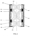
- FIG. 2 illustrates a second electron lens.
- This electron lens is a radially thin-walled cylindrical, magnetic field-type electron lens.
- the electron lens has, inside the radially thin-walled cylindrical ferromagnet 101 located as the outer circumference, a pair of the radially thin-walled cylindrical permanent magnets 112 and 122 installed so as to sandwich the position occupied by the radially thin-walled cylindrical permanent magnet 102 of the first electron lens polarized along the radial direction and a set of magnet coils (correction magnet coils) 114, 115, and 116 each having a general inner diameter equal to the inner diameter of the radially thin-walled cylindrical permanent magnets 112 and 122, and the set of the radially thin-walled cylindrical permanent magnets 112, 122 and the magnet coils 114, 115, 116 generate opposite magnetic fields.
- the electron beam drawing device or the electron beam inspection device for inspecting a substrate using an electron beam has the electron gun and the electron beam optical lens barrel in which a plurality of radially thin-walled cylindrical, magnetic field-type electron lenses are arranged in parallel to the Z axis.
- the permanent magnets 112 and 122 generate magnetic fields in opposite directions, as shown in the figure.
- Three correction magnet coils arranged in the upper, the middle, and the lower portions with respect to the permanent magnets 112 and 122; that is, the correction magnet coil 114 in the upper portion, the correction magnet coil 115 in the middle portion, and the correction magnet coil 116 in the lower portion correct the magnetic fields generated by the permanent magnets 112 and 122.
- the correction magnet coil 114 in the upper portion and the correction magnet coil 116 in the lower portion have almost the same strength and generate magnetic fields in the same direction, while the correction magnet coil 115 in the middle portion has twice the strength of the correction magnet coil 114 in the upper portion and the correction magnet coil 116 in the lower portion and generates a magnetic field in the direction opposite that generated by these coils.
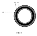
- FIG. 3 shows a cross section of the first electron lens taken along a line A-A' of FIG. 1 .
- the electron lens has the ferromagnet composed of the radially thin-walled cylindrical ferromagnet 101 located as the outer circumference and, inside the radially thin-walled cylindrical ferromagnet located as the outer circumference, the radially thin-walled cylindrical permanent magnet 102 having a length smaller than or equal to approximately a half that of the radially thin-walled cylindrical ferromagnet 101 and polarized along the radial direction.
- this electron lens is the radially thin-walled cylindrical, magnetic field-type electron lens having, inside the radially thin-walled cylindrical permanent magnet, the radially thin-walled cylindrical ferromagnet 103 which is located as the inner circumference and has a length greater than or equal to that of the thin-walled cylindrical permanent magnet 102 in the Z direction.
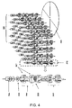
- FIG. 4 shows a multicolumn electron beam drawing device.
- the multicolumn electron beam drawing device has a array 302 in which 10 to more than 250 columns referred to as individual column elements 301 each having a thickness of, for example, approximately 15 mm to 40 mm are arranged two dimensionally. Therefore, it is possible to expose a Si (silicone) wafer 303 (of, for example, 300 mm ⁇ ) at high speed.
- This multicolumn configuration is applicable to the electron beam inspection device for inspecting semiconductor substrates.
- the individual column element 301 is composed of the parts described below.
- An electron beam emitted from an electron gun cathode part 304 is shaped into a rectangular shape at a first rectangular aperture 305 and forms an image on a second rectangular aperture or a CP (character projection) mask 308 using a lens optical system 306 in the first half.
- a position of the beam on the rectangular aperture or the CP mask is provided by reshaping the beam into a beam having a desired size or shape using a beam deflector.
- a rectangular beam having a desired size is formed by two rectangular apertures.
- CP character projection
- the electron beam which has passed through the character is shaped into a desired and intended beam shape according to an aperture formed in the character.
- a lens optical system 309 provided at the subsequent stage deflects the beam to an appropriate position on the wafer 303 to thereby form an image.
- the electron lens systems 306 and 309 are composed of electron lenses 307.
- FIG. 6 illustrates multiple columns and wafers.
- An area of 25 x 25 mm per column is subjected to electron beam drawing or electron beam inspection.
- column elements 501 are aligned at regular intervals at a 25 mm pitch in the horizontal direction (X direction) of the two dimensions and are also aligned at regular intervals at a 25 mm pitch in the vertical direction (Y direction).
- a line 303 indicates an outer circumferential circle of the Si wafer. If approximately half or more of a 25 mm rectangular area drawn by a column element is expected to be located within the outer circumference of the wafer, the column element 501 is installed. In other than these small rectangular areas, column elements are not installed.
- FIG. 6 by providing 120 column elements, the entire wafer can be drawn.
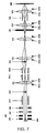
- FIG. 7 shows a vertical cross section of the electron beam drawing device.
- a suppressor electrode 601 and an extraction electrode 602 control an amount of current emission and an emission shape of an electron beam emitted from an electron gun cathode part 600.
- the electron beam subjected to appropriate electrostatic lens action at an electron gun lens electrode 603 is accelerated to 50kV at an anode (earth potential) 604. Further, the beam passes through a blanking deflection electrode 610 and is shaped into a rectangular shape at a first rectangular aperture 605, thereby forming an image on a second rectangular aperture or a CP (character projection) mask 606 through a lens optical system 621 in the first half.
- a blanking deflection electrode 610 is shaped into a rectangular shape at a first rectangular aperture 605, thereby forming an image on a second rectangular aperture or a CP (character projection) mask 606 through a lens optical system 621 in the first half.
- a position on the rectangular aperture or the CP mask is provided by reshaping the beam into a beam having a desired size or shape and deflecting the beam by beam deflectors 611a and 611b such that a crossover image in which beams intersect is not moved, in order to prevent a change in the electron beam density of a finally-formed image.
- a rectangular beam having a desired size is formed by two rectangular apertures.
- CP character projection
- components 621, 622, 623, 624, and 625 are magnetic-field-type lenses each composed of a permanent magnet mainly made of samarium cobalt or a samarium cobalt magnet
- the magnification is adjusted by placing a focus on a precise position using correction coils 631a, 631b, 632a, 632b, 633a, 633b, 634a, 634b, 635a, and 635b each employing an electromagnet, because there is a margin of error of about ⁇ 5% in the focal position and the magnification.
- the permanent magnet When the permanent magnet is used in the electron lens, it is preferable to use a samarium cobalt permanent magnet or a neodymium magnet having a small size and sufficient strength.
- a neodymium magnet is the strongest magnet at present and it is the only magnet that can be polarized along the radial direction when made into a cylindrical ring, it is generally desirable to utilize the neodymium magnet.
- a small and strong permanent magnet has an undesirable characteristic that a magnetic field strength changes depending on a temperature.
- a phenomenon that the neodymium magnet cannot be used at a stable strength unless temperature stabilization is not performed to create change (reduction) of the magnetic field strength by approximately 1100 ppm by changing (increasing) a temperature by one degree Celsius near the normal temperature of 0 degree Celsius.
- a magnetic field strength is changed (reduced) by approximately 300 ppm.
- Such instability of the temperature is caused by changes in the room temperature and heat generated by the correction coils when the permanent magnet does not have an appropriate value for generating a magnetic field.
- the change of the magnetic field strength by 1100 ppm in the neodymium magnet causes, in an electromagnetic lens having a focal depth of 30 mm, a focus change of 33 ⁇ m and a defocus of 165 nm with a convergence half angle of 5 mrad.
- a temperature of the neodymium magnet In order to stabilize the above-described instability to thereby enable the magnet to be used, it is necessary to control a temperature of the neodymium magnet at an accuracy smaller than or equal to 0.001 degree Celsius, at a system operation temperature of approximately 23 degrees Celsius to 24 degrees Celsius. If a temperature is controlled at this level of accuracy, the instability of the focus depth is smaller than or equal to 33 nm, while the defocus is within 0.165 nm and the lateral position shift is within 0.05 nm, and therefore, the magnet is sufficiently capable of being used. In addition, because, in samarium cobalt, under this temperature stabilization condition, the strength variation coefficient due to a temperature change becomes less than or equal to one-third and becomes 0.003 ppm per time, the problem is further alleviated.
- Actual cooling of the neodymium magnet is performed by bathing, in water or an insulating liquid such as Fluorinert, one stage of lens among multicolumn lenses containing a plurality of neodymium magnets. It is possible to control the temperature within a certain temperature range by circulating a liquid coolant, measuring a temperature, and repeating heating and cooling in an alternating manner.
- an insulating liquid such as Fluorinert
- temperature control is required for not only the neodymium magnet but also the entire retainer plate of the first rectangular aperture and the entire retainer plate of the second rectangular aperture, etc. It is important to control a temperature of the entire configuration at each stage along the vertical direction of the multiple columns, in order to ensure the overall positional stability of the beams.
- FIG. 8 shows a lateral cross section of the electron lenses in the multiple columns.
- Each lens is isolated from a vacuum portion 133 through which the electron beam passes by O-rings 109a, 109b, 109c, and 109d and a vacuum sealing cylinder 131.
- a liquid 132 for example, Flourinert
- a temperature of the liquid is stably maintained within a range of less than or equal to 0.001 degrees Celsius.
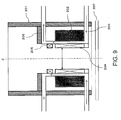
- FIG. 9 shows a configuration of the third electron lens.
- This electron lens has an outer cylinder 201 composed of a thin-walled cylindrical ferromagnet.
- This outer cylinder is made of, for example, pure iron and reduces a fringing field outside the electron lens.
- this ferromagnet outer cylinder 201 it is possible to avoid magnetic field interference caused between adjacent columns when the electron guns are provided in a multicolumn arrangement.
- a permanent magnet (cylindrical permanent magnet) 202 having a diameter smaller than that of the outer cylinder 201 is positioned inside the outer cylinder 201. Unlike the above-described electron lenses, this permanent magnet 202 is polarized along the axial direction (direction in parallel to the Z axis). Therefore, magnetic flux generated by the permanent magnet 202 is emitted from the upper and lower end portions of the permanent magnet 202 (both end portions along the Z axis direction) in the direction parallel to the Z axis, then curves to the center direction, and passes along the central axis (Z axis).
- the permanent magnet 202 is formed of, for example, samarium cobalt. With this permanent magnet 202, the electron beam can be focused.
- a flanged inner cylindrical member 203 which partitions a space inside the outer cylinder 201, contains the permanent magnet 202 in that space, and has flange portions projecting outside from the upper and the lower ends thereof. That is, a doughnut-shaped space is partitioned between by the outer circumferential surface of the flanged inner cylindrical member 203 and the bottom surface and the top surface of the upper and the lower flange portions, and the cylindrical permanent magnet 202 is located within this space.
- an inner circumferential surface of the permanent magnet 202 is in contact with the outer circumferential surface of the flanged inner cylindrical member 203 and the top surface of the lower side flange portion.
- This flanged inner cylindrical member 203 has a hollow center, and this hollow serves as a coolant passage.
- the portion extending in the Z direction has a dual structure as a whole and is in contact with the permanent magnet 202 from inside to cool the permanent magnet 202.
- the coolant is a liquid made of a nonmagnetic material, and various types of commercially available coolants (such as Flourinert) can be employed. Water can also be used.
- the flanged inner cylindrical member 203 is preferably made of a nonmagnetic material such as aluminum.
- the coolant is supplied from the periphery of the lower flange portion and flows laterally through the lower flange portion toward the center portion and then upwardly through the cylindrical portion. The coolant then flows through the upper flange portion toward the periphery and flows to the outside.
- the coolant is supplied from a coolant tank to the flanged inner cylindrical member 203 by means of a pump. After the coolant ejected from flanged inner cylindrical member 203 is cooled by a heat exchanger, etc., it returns to the coolant tank. As described later, the coolant may flow in the opposite direction.
- a cylindrical correction coil 204 is positioned on the inner side of the flanged inner cylindrical member 203. This coil corrects a magnetic field generated by the permanent magnet 202. By means of a current flowing in this coil, it is possible to adjust the magnetic field strength to a predetermined strength. In other words, the cylindrical correction coil 204 is used to compensate for overage and shortage of the magnetic field strength generated by the permanent magnet 202. In this example, a part of the flanged inner cylindrical member 203 is projected toward the inside to support the correction coil 204 from the lower side.
- the outer cylinder 201 is separated into different parts between the upper and the lower sides of the flange portions.
- the flange portion has the coolant passage therein, because it has a sufficient flow passage area and is connected to a conduit in the periphery, it doses not have to have a large cross section serving as a conduit area, and there is no problem even if it is separated into a plurality of portions.
- the passage in the radial direction does not have to have a large cross section, and a conduit may also be adopted.
- the passage may adopt a variety of shapes including, for example, a spiral shape and an S shape, and may also be divided into a plurality of passages.
- a stig coil 205 for shaping an electron beam is provided above the correction coil 204.
- the flanged inner cylindrical member 203 also absorbs heat generated by the stig coil 205.
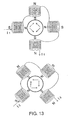
- the stig coil 205 is composed of two sets of coils each including four coils arranged in a cross shape, and the two sets of coils are arranged so that the arrangement directions of the four coils are shifted from those of the other set by 45 degrees along the traveling directions of two beams.
- the two coils facing in the vertical direction both have the S pole on the center side, while the two coils facing in the lateral direction have the N pole on the center side.
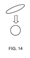
- the figure located on the lower side of FIG. 13 shows a configuration rotated by 45 degrees from the figure on the upper side. Therefore, with the two coils, it is possible to shape a beam passing through the center along a direction perpendicular to the paper and shape an elliptical beam at a random angle to a circular shape, as shown in FIG. 14 .
- a circular plate 206 which has a doughnut shape and is formed of the same magnetic material as the outer cylinder 201 is provided on the upper flange portion of the flanged inner cylindrical member 203, and it partitions the space occupied by the magnetic field of the permanent magnet 202 and the upward space.
- a sample 207 to which the electron beam is emitted is positioned under the above-described configuration, and the electron beam controlled by the electron lens is then emitted to the sample.
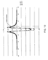
- FIG. 10 shows the magnetic field strength of the electron lens having such a configuration.
- the Z axis is indicated as the lateral axis, and the upper configuration is located on the left side, while the sample is located on the right side.
- the magnetic field strength has a large negative value inside the permanent magnet 202 in the Z axis direction and has certain positive peaks near the upper and the lower sides of the permanent magnet 202.
- the permanent magnet 202 is located at a position between -20 mm to 0 mm, and the sample 207 is located at a position of 10 mm.
- the line connecting between the diamond shaped points indicates a magnet thickness of 12 mm, while the line connecting between the square points (line 2) indicates a magnet thickness of 10 mm.
- the electron lens having such a configuration, it is possible to focus the electron beam narrowly and reduce occurrence of aberration of the electron lens depending on a temperature.
- a permanent magnet lens which can form a magnetic field using a large and thick lens, in a space of 20 mm to 30 mm immediately above the sample (wafer) to which the electron beam is applied.
- the present electron lens employs the permanent magnet 202 which is polarized along the cylindrical axis direction.
- the first peak is directed to the positive direction as shown in FIG. 10 .
- the beam-focusing strength acts proportionally to the amount obtained by integrating a square of a magnetic field B along the Z axis direction, and the magnetic field of the lens is long along the Z direction and strong near the sample. Therefore, the lens generating a magnetic field has a small spherical aberration.
- the sample surface is preferably located in the middle of the second positive peak of the magnetic field in FIG. 10 .
- the relatively long negative magnetic field can be used as an effective lens magnetic field, and as the sample surface is near this magnetic field, the working distance becomes short.
- cooling is performed by circulating the coolant in the above-described flanged inner cylindrical member 203, in order to ensure the thermal stability of the permanent magnet 202.
- the permanent magnet 202 is made of samarium cobalt, the magnetic field strength changes at a temperature coefficient of 300 ppm/degree Celsius (a change of magnetic field strength per one degree is 300/million).
- the temperature of the permanent magnet 202 is controlled so that a temperature change of 3 m degree K is obtained, it is possible to maintain a stability of 1 ppm/degree Celsius.
- the coolant for example, Flourinert which is a fluorine inactive liquid and has high thermal conductivity.
- the permanent magnet 202, etc. vibrates due to circulation of the coolant, focus of the electron beam is adversely affected. Therefore, it is necessary to make an arrangement to circulate the coolant smoothly so as not to transmit minute vibrations.
- the coolant thermally separates the components generating Joule heat, such as the correction coil 204 and the stig coil 205, from the permanent magnet 202. In doing so, the temperature stability of the permanent magnet 202 is also ensured.
- FIG. 11 shows a schematic view of a conduit for the coolant.
- a fluid entered from the upper flange portion of the electron lens passes through the cylindrical member and exits from the lower flange portion
- a fluid entered from the lower flange portion passes through the cylindrical member and exits from the lower flange portion
- solid lines indicate that the fluid reaches the flanged inner cylindrical member 203 of the adjacent column on the upper side
- the dotted lines indicate that the fluid reaches the flanged inner cylindrical member 203 of the adjacent column on the lower side.
- the coolant After passing through the upper flange portion, the coolant enters the upper flange portion of the next lens and then passes through a cylindrical member between the coil and the permanent magnet in the center portion toward the lower flange portion.
- the fluid flows in one direction while repeating passage through such flow passages in an alternating manner. In this example, after entering from the flow passage on the left end, the fluid is separated into four lines. The fluid then passes through the respective flow passages and exits from the flow passage on the right end.
- the correction coil 204 it is necessary to estimate the amount of Joule heat generated by the correction coil 204.
- a magnet coil generates a heat of 300 to 500 W per lens as Joule heat.
- the correction coil 204 has a margin of error of ⁇ 5% with respect to the polarized magnetic field of the permanent magnet 202. Therefore, the amount of heat generation is 0.25%, which is below 1.25 W. Even if there are one hundred lenses, the amount remains 125 W; that is, 30 Cal.
- thermometers to various parts of the lens and returning the fluid to a chiller as a storage tank of the coolant. That is, there is no need to use a special heat exchanger, etc.
- FIG. 12 shows a fourth electron lens in which the inside and outside relationship between the permanent magnet 202 and the correction coil 204 are changed from the third electron lens.
- the doughnut-shaped circular plate 206 made of a ferromagnetic material is omitted. This is because the circular plate 206 is used to match the magnetic potential within the same plane, and therefore, it is not essential in the electromagnetic lens.
- the permanent magnet 202 may be located inside or may be located outside, so long as the permanent magnet 202 and the correction coil 204 are thermally separated by the flowing coolant.
- the permanent magnet 202 is located inside, while the correction coil 204 is located outside, and the flanged inner cylindrical member 203 for circulating the coolant is provided between them.
- the permanent magnet 202 may be an integral cylindrical permanent magnet as in the third electron lens
- the permanent magnet 202 has a configuration divided into a plurality of pieces along the axis direction, in consideration of non-uniform magnetic field strength along the axis and degradation of the axial asymmetry. That is, the permanent magnet 202 is formed by stacking, along the axial direction, divided ring magnets 202a, 202c, 202e, 202g, and 202i which are integrally made of samarium cobalt and have a short length in the axial direction. Therefore, each of the divided ring magnets 202a, 202c, 202e, 202g, and 202i has a thickness of approximately one-fifth the overall thickness.
- ring plates 202b, 202d, 202f, and 202h having a thin-walled circular ring plate shape are positioned along the axial direction in the gaps among the divided ring magnets 202a, 202c, 202e, 202g, and 202i.
- These ring plates 202b, 202d, 202f, and 202h are made of a nonmagnetic material such as aluminum, or of different types of permanent magnets, such as pure iron serving as a ferromagnet and permanent magnet neodymium.
- the permanent magnet 202 is an integral cylinder and equivalent electromagnetic lenses are manufactured, there are cases where the magnetic field strength distribution is not uniform along the central Z axis, and the magnetic field vector is distorted from the Z axis. For example, variation of the magnetic field strength may be approximately plus or minus 5%.
- a target strength is determined in advance to be a relatively weak strength around an average value, and if the strength of the divided ring magnets 202a, 202c, 202e, 202g, and 202i is higher than the average value of the parts, the nonmagnetic ring plates 202b, 202d, 202f, and 202h are sandwiched between joint portions, whereas when the strength is weaker than the average value, the ferromagnet ring plates 202b, 202d, 202f, and 202h are sandwiched between the joint portions in a direction to strengthen the magnetic field.
- a magnetic field vector toward the Z axis is tilted, by assembling the individual divided ring magnets 202a, 202c, 202e, 202g, and 202i while rotating them, the magnetic field strength obtained by summing the five divided ring magnets 202a, 202c, 202e, 202g, and 202i becomes closer to the target value, and the configuration can be assembled such that the magnetic field vector along the central Z axis direction becomes closest to a straight line.
- the ring permanent magnet 202 In order to smooth the non-uniformity in the axial symmetry of the magnetic field along the Z axis direction, the ring permanent magnet 202; that is, the magnets 202a, 202c, 202e, 202g, and 202i, may be vertically sandwiched between thin ferromagnetic circular plates made of, for example, permalloy, pure iron, or permendur (also referred to as permendur).
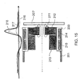
- FIG. 15 A first embodiment of the invention as claimed will now be described by reference to FIG. 15 .
- a thin-walled ferromagnetic ring 211 is located on the sample 207 side of a cylindrical permanent magnet 212 which forms the electron lens; that is, the end surface on the electron beam emission side.
- the inner diameter of the ferromagnetic ring 211 is almost the same as that of the cylindrical permanent magnet 212, its outer diameter is smaller than the outer diameter of the cylindrical permanent magnet 212, and the width of the ferromagnetic ring 211 in the radial direction is approximately one-third the width of the cylindrical permanent magnet 212 in the radial direction.
- the outer diameter of the ferromagnetic ring 211 is almost the same as the inner diameter of a cylindrical permanent magnet 213, which will be described later.
- the ferromagnetic ring 211 is a thin-walled ferromagnetic ring which is used to make a uniform magnetic field and protect the lens characteristics from the adverse effect caused by the axially asymmetric magnetic field generated around the Z axis by the cylindrical permanent magnet 212.
- the electron lens utilizing the permanent magnet it is necessary to reduce a spherical aberration coefficient of the lens by generating a strong magnetic field in the immediate vicinity of the surface of the sample 207 on which drawing is performed. This is because, in order to reduce the aberration caused by Coulomb repulsion, it is necessary to provide a large convergence half angle ⁇ of a beam, and, normally, if ⁇ is a value as large as approximately 10 mrad, the beam defocus remains a value as small as approximately 10 nm even if a large sample current value of 300 nA is adopted.
- a strong magnetic field of greater than 4000 Gauss has to be generated at a height of approximately 10 mm above the surface of the sample 207 to make the spherical aberration coefficient less than or equal to 10 mm.
- the cylindrical permanent magnet 212 has to be made of samarium cobalt polarized along the axis direction and has a hole diameter (inner diameter) smaller than or equal to 6 mm.
- cylindrical permanent magnet 213 serving as an electron lens having a large hole diameter (large inner diameter) is installed along the electron beam incoming direction (incoming side) so that the polarity is opposite that of the cylindrical permanent magnet 212.
- a magnetic field distribution curve 216 is obtained by the cylindrical permanent magnet 212 serving as a main permanent magnet. Meanwhile, a magnetic field generated by the cylindrical permanent magnet 213 serving as a sub electron lens resembles a magnetic field distribution curve 217. Therefore, a magnetic field obtained by an electron lens generated by adding the two curves; that is, by combining the two cylindrical permanent magnets 212 and 213, has a local maximum value in the magnetic field portion immediately above the surface of the sample 207, like a magnetic field distribution curve 218. As, in the Z direction, an integrated value of a square of the magnetic field along the Z direction is equal to the lens strength, it is possible to obtain a small spherical aberration due to the strong magnetic field immediately above the surface of the sample 207.
- the inner diameter of the main permanent magnet lens is greater than or equal to 8 mm, it is possible to achieve a lens which has a beam convergence half angle ⁇ of 10 mrad with a small change in the depth of beam focus due to the Coulomb effect, a spherical aberration coefficient of 10 nm, and a spherical aberration of approximately 10 nm. If the permanent magnet lenses (cylindrical permanent magnets 212 and 213) have a small inner diameter, a deflector cannot be installed. Therefore, the inner diameter is preferably as large as possible.
- the ferromagnetic ring 211 is provided on the end surface of the cylindrical permanent magnet 212 facing the sample 207, it is possible to make a uniform magnetic field immediately above the sample 207 in the circumferential direction, thereby obtaining an electron lens with high accuracy.
- correction coils 214 and 215 for correcting the magnetic field strength of the permanent magnets are installed immediately inside the cylindrical ferromagnet 201.
- the correction coils 214 and 215 are provided so as to correspond to the cylindrical permanent magnets 212 and 213, respectively, and the respective correction coils generate appropriate correction magnet fields, one or more than two correction coils may be provided.
- the flanged inner cylindrical member (coolant passage) 203 is also formed so as to prevent heat generated by the correction coils 214 and 215 from being transmitted to the cylindrical permanent magnets 212 and 213.
- the cylindrical permanent magnets 212 and 213 may have a configuration formed of a plurality of divided pieces or a configuration having the magnetic material inside.
- FIG. 16 shows a variant of the first embodiment of the claimed invention.
- cylindrical permanent magnet 219 polarized along the radial direction is provided in place of the above-described cylindrical permanent magnet 213.
- This cylindrical permanent magnet 219 is polarized along the radial direction so that the magnetic field generated on the cylindrical permanent magnet 212 side can be a magnetic field that strengthens the main-lens magnetic field of the cylindrical permanent magnet 212. With this configuration, it is also possible to strengthen the magnetic field in the vicinity of an electron beam emitting portion.
- the multicolumn electron beam drawing device is the most likely technology to expose an LSI pattern of a line width of 15 nm to 10 nm, which will be required in the years 2015 to 2020, at a processing capacity of approximately 10 sheets to more than approximately 20 sheets of 300 mm wafers per hour.
- Other proposed technologies such as, for example, an extremely short ultraviolet exposure device are likely to have a processing capacity of approximately only one sheet per hour.
- an LSI pattern having a line width of approximately 15 nm to approximately 10 nm can be exposed using only photoresist (photosensitive substance) having a sensitivity lower than 100 ⁇ C/cm 2
- a beam is defocused by a large current caused by inter-electron interaction, and therefore, only a current value of approximately several microamperes per column can be used.
- the 300 mm wafer has an area of approximately 600 square centimeters, an exposure time of more than 60,000 seconds is required. With more than several dozens of columns, it is possible to reduce this time to approximately 600 seconds or less.
- CP character projection
- the thickness of a column element is estimated.
- the diameter of the thickness of the column element has to be smaller than or equal to 25 mm.
- the column according to the present invention can be made 25 mm or smaller, which is a fraction of the size of the conventional column, and therefore, it is possible to arrange several dozens to one hundred multiple columns for providing lenses.
- the present technology is considered to be essential in the configuration of the multicolumn electron beam drawing device and greatly contribute to the electronic industry as a technology providing practical use of the multicolumn electron beam drawing device and playing a central role of the next generation fine lithography.
Landscapes
- Chemical & Material Sciences (AREA)
- Engineering & Computer Science (AREA)
- Analytical Chemistry (AREA)
- Nanotechnology (AREA)
- Physics & Mathematics (AREA)
- Crystallography & Structural Chemistry (AREA)
- Theoretical Computer Science (AREA)
- Mathematical Physics (AREA)
- Condensed Matter Physics & Semiconductors (AREA)
- General Physics & Mathematics (AREA)
- Manufacturing & Machinery (AREA)
- Plasma & Fusion (AREA)
- Electromagnetism (AREA)
- Electron Beam Exposure (AREA)
Claims (6)
- Elektronenlinse zur Benutzung in einem Elektronenstrahlgerät mit einer Elektronenkanone zum Emittieren eines Elektronenstrahls in eine Richtung einer Z-Achse, mit:einem äußeren Zylinder (201) mit einem zylindrischen Ferromagneten mit der Z-Achse als Mittelachse;einem zylindrischen Permanentmagneten (202), der innerhalb des äußeren Zylinders angeordnet und entlang der Richtung der Z-Achse polarisiert ist;einer Korrekturspule (204), die innerhalb oder außerhalb des zylindrischen Permanentmagneten mit einem Spalt zu dem zylindrischen Permanentmagneten angeordnet ist, zum Einstellen einer magnetischen Feldstärke, die durch den zylindrischen Permanentmagneten entlang der Richtung der Z-Achse erzeugt wird; undeinem Kühlmitteldurchlass (203), der in dem Spalt zwischen dem zylindrischen Permanentmagneten und der Korrekturspule angeordnet ist, um es einem Kühlmittel zu erlauben, durch diesen hlndurchzufüeßen und Temperaturwechsel in dem zylindrischen Permanent-magneten zu steuern oder zu regeln;
dadurch gekennzeichnet, dassein dünner ferromagnetischer Ring (211), der ein durch den zylindrischen Permanentmagneten erzeugtes magnetisches Feld homogenisiert, auf einer Endoberfläche einer Elektronenstrahlemissionsseite des zylindrischen Permanentmagneten entlang der Richtung der Z-Achse angeordnet ist. - Elektronenlinse nach Anspruch 1, dadurch gekennzeichnet, dass
der zylindrische Permanentmagnet einen auf einer Elektronenstrahleingangsseite angeordneten ersten zylindrischen Permanentmagneten (105) und einen auf der Elektronenstrahlemissionsseite angeordneten zweiten zylindrischen Permanentmagneten (106) aufweist, wobei beide zylindrischen Permanentmagneten entlang der Richtung der Z-Achse ausgerichtet sind;
der erste zylindrische Permanentmagnet und der zweite zylindrische Permanentmagnet so polarisiert sind, dass sie Magnetfelder in entgegengesetzten Richtungen erzeugen;
der erste zylindrische Permanentmagnet einen größeren Innendurchmesser als der zweite zylindrische Permanentmagnet hat; und
sich ein durch den zweiten zylindrischen Permanentmagneten erzeugtes zentrales Magnetfeld mit einem durch den ersten zylindrischen Permanentmagneten erzeugten zentralen Magnetfeld überdeckt. - Elektronenlinse nach Anspruch 2, weiterhin gekennzeichnet durch einen weiteren zylindrischen Permanentmagneten (112), der auf der Elektronenstrahleingangsseite des zylindrischen Permanentmagneten angeordnet ist, wobei
der weitere zylindrische Permanentmagnet entlang einer radialen Richtung so polarisiert ist, dass ein auf der Seite des zylindrischen Permanentmagneten erzeugtes Magnetfeld ein Magnetfeld ist, welches das durch den zylindrischen Permanentmagneten erzeugte Magnetfeld verstärkt. - Elektronenlinse nach einem der Ansprüche 1 bis 3, dadurch gekennzeichnet, dass der Kühlmitteldurchlass (203) einen in dem Spalt angeordneten zylindrischen Durchlass besitzt.
- Elektronenlinse nach Anspruch 1, dadurch gekennzeichnet, dass der Innendurchmesser des dünnen ferromagnetischen Rings (211) fast der Gleiche ist wie der des zylindrischen Permanentmagneten und sein Außendurchmesser kleiner ist als der Außendurchmesser des zylindrischen Permanentmagneten.
- Elektronenstrahlgerät (302) mit einer Mehrzahl von Elektronenlinsen (307) nach einem der Ansprüche 1 bis 5, die in einer im Wesentlichen senkrecht zu einer Z-Achse verlaufenden Ebene angeordnet sind, das eine Mehrzahl von Elektronenstrahlen auf eine Probe emittiert.
Applications Claiming Priority (2)
| Application Number | Priority Date | Filing Date | Title |
|---|---|---|---|
| JP2010240408 | 2010-10-27 | ||
| PCT/JP2011/074588 WO2012057166A1 (ja) | 2010-10-27 | 2011-10-25 | 電子レンズおよび電子ビーム装置 |
Publications (3)
| Publication Number | Publication Date |
|---|---|
| EP2587517A1 EP2587517A1 (de) | 2013-05-01 |
| EP2587517A4 EP2587517A4 (de) | 2014-05-07 |
| EP2587517B1 true EP2587517B1 (de) | 2015-09-09 |
Family
ID=45993872
Family Applications (1)
| Application Number | Title | Priority Date | Filing Date |
|---|---|---|---|
| EP11836299.5A Not-in-force EP2587517B1 (de) | 2010-10-27 | 2011-10-25 | Elektronenobjektiv und elektronenstrahlvorrichtung |
Country Status (7)
| Country | Link |
|---|---|
| US (2) | US20130134322A1 (de) |
| EP (1) | EP2587517B1 (de) |
| JP (1) | JP5148014B2 (de) |
| KR (1) | KR101861210B1 (de) |
| CN (1) | CN103038855B (de) |
| TW (1) | TWI539483B (de) |
| WO (1) | WO2012057166A1 (de) |
Families Citing this family (25)
| Publication number | Priority date | Publication date | Assignee | Title |
|---|---|---|---|---|
| JP5504277B2 (ja) * | 2009-11-26 | 2014-05-28 | 株式会社日立ハイテクノロジーズ | 走査電子顕微鏡 |
| JP6114981B2 (ja) * | 2012-10-17 | 2017-04-19 | 株式会社リガク | X線発生装置 |
| JP5667618B2 (ja) * | 2012-12-14 | 2015-02-12 | 株式会社アドバンテスト | 電磁レンズ及び電子ビーム露光装置 |
| JP6061686B2 (ja) * | 2013-01-11 | 2017-01-18 | 株式会社日立ハイテクノロジーズ | 荷電粒子線装置及びその収差補正方法 |
| JP6323943B2 (ja) * | 2013-02-27 | 2018-05-16 | 株式会社Param | 電子レンズおよび電子ビーム装置 |
| CN104217779B (zh) | 2014-09-15 | 2015-09-23 | 华中科技大学 | 一种电子束扩散截面修整装置及方法 |
| JP6470124B2 (ja) * | 2015-06-19 | 2019-02-13 | 株式会社東芝 | 粒子線ビームの制御電磁石及びこれを備えた照射治療装置 |
| JP2017135218A (ja) * | 2016-01-26 | 2017-08-03 | 株式会社アドバンテスト | 荷電粒子ビームレンズ装置、荷電粒子ビームカラム、および荷電粒子ビーム露光装置 |
| US10211021B2 (en) * | 2016-04-11 | 2019-02-19 | Kla-Tencor Corporation | Permanent-magnet particle beam apparatus and method incorporating a non-magnetic metal portion for tunability |
| WO2018042531A1 (ja) * | 2016-08-31 | 2018-03-08 | 株式会社日立ハイテクノロジーズ | 計測装置及び計測方法 |
| JP6872380B2 (ja) * | 2017-02-03 | 2021-05-19 | 日立造船株式会社 | ノズル式電子線照射装置 |
| WO2018189817A1 (ja) | 2017-04-11 | 2018-10-18 | 株式会社アドバンテスト | 露光装置 |
| KR102271664B1 (ko) | 2017-04-11 | 2021-07-01 | 주식회사 아도반테스토 | 노광 장치 |
| TWI744671B (zh) * | 2018-08-03 | 2021-11-01 | 日商紐富來科技股份有限公司 | 電子光學系統及多射束圖像取得裝置 |
| CN109065428B (zh) * | 2018-08-16 | 2020-10-09 | 电子科技大学 | 一种双栅控制式冷阴极电子枪及其制备方法 |
| CZ2018584A3 (cs) * | 2018-10-28 | 2020-02-05 | DELONG INSTRUMENTS a. s. | Korektor sférické vady v zařízení se svazkem nabitých částic a způsob korigování sférické vady další čočky, typicky objektivové čočky, tímto korektorem |
| EP3881347A1 (de) * | 2018-11-16 | 2021-09-22 | ASML Netherlands B.V. | Elektromagnetische zusammengesetzte linse und optisches system mit geladenen teilchen mit einer solchen linse |
| US20220065727A1 (en) * | 2020-08-28 | 2022-03-03 | Kla Corporation | Coolant Microleak Sensor for a Vacuum System |
| NL2027307B1 (en) * | 2021-01-13 | 2022-07-25 | Vdl Enabling Tech Group B V | A charged particle lens assembly and a charged particle beam apparatus provided with such charged particle lens assembly. |
| WO2022230717A1 (ja) * | 2021-04-28 | 2022-11-03 | 株式会社ニコン | 荷電粒子光学系および荷電粒子装置 |
| US12500060B2 (en) | 2021-07-14 | 2025-12-16 | Ims Nanofabrication Gmbh | Electromagnetic lens |
| CN114791332B (zh) * | 2022-04-06 | 2023-09-15 | 安徽蓝格利通新材应用股份有限公司 | 一种真空绝热板自动检测装置 |
| CN115498589B (zh) * | 2022-11-18 | 2023-03-31 | 国网天津市电力公司电力科学研究院 | 一种电缆终端无源加热保温装置及制备方法 |
| JP7811572B2 (ja) * | 2022-12-22 | 2026-02-05 | アイエムエス ナノファブリケーション ゲーエムベーハー | 荷電粒子レンズ、電磁レンズ及び荷電粒子光学装置 |
| TW202544855A (zh) * | 2023-12-21 | 2025-11-16 | 荷蘭商Asml荷蘭公司 | 帶電粒子束設備中之熱變形補償 |
Family Cites Families (20)
| Publication number | Priority date | Publication date | Assignee | Title |
|---|---|---|---|---|
| US2853657A (en) * | 1945-09-04 | 1958-09-23 | Henry B Hofacker | Magnets |
| US3164739A (en) * | 1960-07-20 | 1965-01-05 | Vakutronik Veb | Ion source of a duo-plasmatron |
| US3336526A (en) * | 1963-12-30 | 1967-08-15 | Varian Associates | Superconducting magnet |
| US4433270A (en) * | 1980-01-28 | 1984-02-21 | Drozdov Sergei S | Reversible periodic magnetic focusing system |
| JPS60245132A (ja) * | 1984-05-21 | 1985-12-04 | Toshiba Corp | 電子ビ−ム露光装置等の電子レンズ |
| GB2192092A (en) * | 1986-06-25 | 1987-12-31 | Philips Electronic Associated | Magnetic lens system |
| JPS63244546A (ja) * | 1987-03-30 | 1988-10-12 | Seiko Instr & Electronics Ltd | 永久磁石を用いた多重極レンズ |
| US4731598A (en) * | 1987-08-24 | 1988-03-15 | The United States Of America As Represented By The Secretary Of The Army | Periodic permanent magnet structure with increased useful field |
| US4975668A (en) * | 1988-04-26 | 1990-12-04 | Kanto Denshi Kogyo Co., Ltd. | Electromagnetic focusing |
| JP2551867Y2 (ja) | 1991-03-29 | 1997-10-27 | 日本電気ホームエレクトロニクス株式会社 | フォーカスマグネット |
| JPH05128986A (ja) * | 1991-11-06 | 1993-05-25 | Jeol Ltd | 磁場型レンズ |
| JP3325982B2 (ja) * | 1993-12-27 | 2002-09-17 | 株式会社東芝 | 磁界界浸型電子銃 |
| EP1120809B1 (de) * | 2000-01-27 | 2012-02-22 | ICT Integrated Circuit Testing Gesellschaft für Halbleiterprüftechnik mbH | Objektivlinse für eine Ladungsträgerstrahl-Vorrichtung |
| US6392231B1 (en) | 2000-02-25 | 2002-05-21 | Hermes-Microvision, Inc. | Swinging objective retarding immersion lens electron optics focusing, deflection and signal collection system and method |
| US6750455B2 (en) * | 2001-07-02 | 2004-06-15 | Applied Materials, Inc. | Method and apparatus for multiple charged particle beams |
| KR100813210B1 (ko) * | 2002-03-21 | 2008-03-13 | 헤르메스-마이크로비전 인코포레이티드 | 진동 지연 침지 대물 렌즈의 전자 광 포커싱, 검출 및신호 수집 시스템 및 방법 |
| GB2408143B (en) * | 2003-10-20 | 2006-11-15 | Ims Nanofabrication Gmbh | Charged-particle multi-beam exposure apparatus |
| JP4795847B2 (ja) | 2006-05-17 | 2011-10-19 | 株式会社日立ハイテクノロジーズ | 電子レンズ及びそれを用いた荷電粒子線装置 |
| EP1970935B1 (de) * | 2007-03-14 | 2011-01-12 | ICT, Integrated Circuit Testing Gesellschaft für Halbleiterprüftechnik mbH | Kühlung der Spule einer Magnetlinse |
| EP2302664B1 (de) * | 2008-06-24 | 2013-11-06 | Advantest Corporation | MEHRSÄULEN-ELEKTRONENSTRAHLBELICHTUNGSVORRICHTUNG UND Vorrichtung zur Erzeugung eines Magnetfeldes |
-
2011
- 2011-10-25 CN CN201180037664.XA patent/CN103038855B/zh not_active Expired - Fee Related
- 2011-10-25 JP JP2012511468A patent/JP5148014B2/ja not_active Expired - Fee Related
- 2011-10-25 US US13/814,190 patent/US20130134322A1/en not_active Abandoned
- 2011-10-25 EP EP11836299.5A patent/EP2587517B1/de not_active Not-in-force
- 2011-10-25 KR KR1020137000919A patent/KR101861210B1/ko not_active Expired - Fee Related
- 2011-10-25 WO PCT/JP2011/074588 patent/WO2012057166A1/ja not_active Ceased
- 2011-10-27 TW TW100139001A patent/TWI539483B/zh not_active IP Right Cessation
-
2014
- 2014-05-07 US US14/271,940 patent/US9418815B2/en not_active Expired - Fee Related
Also Published As
| Publication number | Publication date |
|---|---|
| WO2012057166A1 (ja) | 2012-05-03 |
| EP2587517A4 (de) | 2014-05-07 |
| TW201225144A (en) | 2012-06-16 |
| US20130134322A1 (en) | 2013-05-30 |
| TWI539483B (zh) | 2016-06-21 |
| KR101861210B1 (ko) | 2018-05-25 |
| KR20130138713A (ko) | 2013-12-19 |
| CN103038855A (zh) | 2013-04-10 |
| JPWO2012057166A1 (ja) | 2014-05-12 |
| US9418815B2 (en) | 2016-08-16 |
| JP5148014B2 (ja) | 2013-02-20 |
| US20140252245A1 (en) | 2014-09-11 |
| CN103038855B (zh) | 2016-02-03 |
| EP2587517A1 (de) | 2013-05-01 |
Similar Documents
| Publication | Publication Date | Title |
|---|---|---|
| EP2587517B1 (de) | Elektronenobjektiv und elektronenstrahlvorrichtung | |
| US8390201B2 (en) | Multi-column electron beam exposure apparatus and magnetic field generation device | |
| US20090032722A1 (en) | Corrector for charged-particle beam aberration and charged-particle beam apparatus | |
| US12500060B2 (en) | Electromagnetic lens | |
| JP5667618B2 (ja) | 電磁レンズ及び電子ビーム露光装置 | |
| TWI469177B (zh) | 用於帶電粒子束的鏡片系統、裝置及方法 | |
| US20230360878A1 (en) | Adjustable Permanent Magnetic Lens Having Shunting Device | |
| WO2012062854A1 (en) | Lithography system and method of refracting | |
| US20240021403A1 (en) | Adjustable Permanent Magnetic Lens Having Thermal Control Device | |
| JP6544567B2 (ja) | 電子レンズおよびマルチコラム電子ビーム装置 | |
| US12009175B2 (en) | Charged particle beam writing apparatus | |
| US20240212970A1 (en) | Adjustable Magnetic Lens Having Permanent-Magnetic and Electromagnetic Components | |
| KR101248126B1 (ko) | 이온원 | |
| KR102921229B1 (ko) | 하전 입자 빔 제어 디바이스, 및 그것을 구비하는 하전 입자 빔 장치 | |
| JP2007035386A (ja) | 電子線装置及び該装置を用いたデバイス製造方法 | |
| JP2005032574A (ja) | 板状コイル、トロイダル型コイル構造体および荷電粒子線露光装置 |
Legal Events
| Date | Code | Title | Description |
|---|---|---|---|
| PUAI | Public reference made under article 153(3) epc to a published international application that has entered the european phase |
Free format text: ORIGINAL CODE: 0009012 |
|
| 17P | Request for examination filed |
Effective date: 20130122 |
|
| AK | Designated contracting states |
Kind code of ref document: A1 Designated state(s): AL AT BE BG CH CY CZ DE DK EE ES FI FR GB GR HR HU IE IS IT LI LT LU LV MC MK MT NL NO PL PT RO RS SE SI SK SM TR |
|
| DAX | Request for extension of the european patent (deleted) | ||
| A4 | Supplementary search report drawn up and despatched |
Effective date: 20140408 |
|
| RIC1 | Information provided on ipc code assigned before grant |
Ipc: H01L 21/027 20060101ALI20140402BHEP Ipc: H01J 37/305 20060101ALI20140402BHEP Ipc: H01J 37/141 20060101ALI20140402BHEP Ipc: H01J 37/143 20060101AFI20140402BHEP Ipc: H01J 37/317 20060101ALI20140402BHEP |
|
| RIC1 | Information provided on ipc code assigned before grant |
Ipc: H01J 37/141 20060101ALI20150130BHEP Ipc: H01J 37/317 20060101ALI20150130BHEP Ipc: H01L 21/027 20060101ALI20150130BHEP Ipc: H01J 37/143 20060101AFI20150130BHEP Ipc: H01J 37/305 20060101ALI20150130BHEP |
|
| GRAP | Despatch of communication of intention to grant a patent |
Free format text: ORIGINAL CODE: EPIDOSNIGR1 |
|
| INTG | Intention to grant announced |
Effective date: 20150428 |
|
| RIN1 | Information on inventor provided before grant (corrected) |
Inventor name: YASUDA HIROSHI |
|
| GRAS | Grant fee paid |
Free format text: ORIGINAL CODE: EPIDOSNIGR3 |
|
| GRAA | (expected) grant |
Free format text: ORIGINAL CODE: 0009210 |
|
| AK | Designated contracting states |
Kind code of ref document: B1 Designated state(s): AL AT BE BG CH CY CZ DE DK EE ES FI FR GB GR HR HU IE IS IT LI LT LU LV MC MK MT NL NO PL PT RO RS SE SI SK SM TR |
|
| RAP1 | Party data changed (applicant data changed or rights of an application transferred) |
Owner name: PARAM CORPORATION |
|
| REG | Reference to a national code |
Ref country code: GB Ref legal event code: FG4D |
|
| REG | Reference to a national code |
Ref country code: AT Ref legal event code: REF Ref document number: 748720 Country of ref document: AT Kind code of ref document: T Effective date: 20150915 Ref country code: CH Ref legal event code: EP |
|
| REG | Reference to a national code |
Ref country code: IE Ref legal event code: FG4D |
|
| REG | Reference to a national code |
Ref country code: DE Ref legal event code: R096 Ref document number: 602011019713 Country of ref document: DE |
|
| REG | Reference to a national code |
Ref country code: NL Ref legal event code: MP Effective date: 20150909 |
|
| PG25 | Lapsed in a contracting state [announced via postgrant information from national office to epo] |
Ref country code: GR Free format text: LAPSE BECAUSE OF FAILURE TO SUBMIT A TRANSLATION OF THE DESCRIPTION OR TO PAY THE FEE WITHIN THE PRESCRIBED TIME-LIMIT Effective date: 20151210 Ref country code: LT Free format text: LAPSE BECAUSE OF FAILURE TO SUBMIT A TRANSLATION OF THE DESCRIPTION OR TO PAY THE FEE WITHIN THE PRESCRIBED TIME-LIMIT Effective date: 20150909 Ref country code: LV Free format text: LAPSE BECAUSE OF FAILURE TO SUBMIT A TRANSLATION OF THE DESCRIPTION OR TO PAY THE FEE WITHIN THE PRESCRIBED TIME-LIMIT Effective date: 20150909 Ref country code: FI Free format text: LAPSE BECAUSE OF FAILURE TO SUBMIT A TRANSLATION OF THE DESCRIPTION OR TO PAY THE FEE WITHIN THE PRESCRIBED TIME-LIMIT Effective date: 20150909 Ref country code: NO Free format text: LAPSE BECAUSE OF FAILURE TO SUBMIT A TRANSLATION OF THE DESCRIPTION OR TO PAY THE FEE WITHIN THE PRESCRIBED TIME-LIMIT Effective date: 20151209 |
|
| REG | Reference to a national code |
Ref country code: LT Ref legal event code: MG4D |
|
| REG | Reference to a national code |
Ref country code: AT Ref legal event code: MK05 Ref document number: 748720 Country of ref document: AT Kind code of ref document: T Effective date: 20150909 |
|
| PG25 | Lapsed in a contracting state [announced via postgrant information from national office to epo] |
Ref country code: RS Free format text: LAPSE BECAUSE OF FAILURE TO SUBMIT A TRANSLATION OF THE DESCRIPTION OR TO PAY THE FEE WITHIN THE PRESCRIBED TIME-LIMIT Effective date: 20150909 Ref country code: ES Free format text: LAPSE BECAUSE OF FAILURE TO SUBMIT A TRANSLATION OF THE DESCRIPTION OR TO PAY THE FEE WITHIN THE PRESCRIBED TIME-LIMIT Effective date: 20150909 Ref country code: HR Free format text: LAPSE BECAUSE OF FAILURE TO SUBMIT A TRANSLATION OF THE DESCRIPTION OR TO PAY THE FEE WITHIN THE PRESCRIBED TIME-LIMIT Effective date: 20150909 Ref country code: SE Free format text: LAPSE BECAUSE OF FAILURE TO SUBMIT A TRANSLATION OF THE DESCRIPTION OR TO PAY THE FEE WITHIN THE PRESCRIBED TIME-LIMIT Effective date: 20150909 |
|
| PG25 | Lapsed in a contracting state [announced via postgrant information from national office to epo] |
Ref country code: NL Free format text: LAPSE BECAUSE OF FAILURE TO SUBMIT A TRANSLATION OF THE DESCRIPTION OR TO PAY THE FEE WITHIN THE PRESCRIBED TIME-LIMIT Effective date: 20150909 |
|
| PG25 | Lapsed in a contracting state [announced via postgrant information from national office to epo] |
Ref country code: EE Free format text: LAPSE BECAUSE OF FAILURE TO SUBMIT A TRANSLATION OF THE DESCRIPTION OR TO PAY THE FEE WITHIN THE PRESCRIBED TIME-LIMIT Effective date: 20150909 Ref country code: CZ Free format text: LAPSE BECAUSE OF FAILURE TO SUBMIT A TRANSLATION OF THE DESCRIPTION OR TO PAY THE FEE WITHIN THE PRESCRIBED TIME-LIMIT Effective date: 20150909 Ref country code: IT Free format text: LAPSE BECAUSE OF FAILURE TO SUBMIT A TRANSLATION OF THE DESCRIPTION OR TO PAY THE FEE WITHIN THE PRESCRIBED TIME-LIMIT Effective date: 20150909 Ref country code: IS Free format text: LAPSE BECAUSE OF FAILURE TO SUBMIT A TRANSLATION OF THE DESCRIPTION OR TO PAY THE FEE WITHIN THE PRESCRIBED TIME-LIMIT Effective date: 20160109 Ref country code: SK Free format text: LAPSE BECAUSE OF FAILURE TO SUBMIT A TRANSLATION OF THE DESCRIPTION OR TO PAY THE FEE WITHIN THE PRESCRIBED TIME-LIMIT Effective date: 20150909 |
|
| PG25 | Lapsed in a contracting state [announced via postgrant information from national office to epo] |
Ref country code: RO Free format text: LAPSE BECAUSE OF FAILURE TO SUBMIT A TRANSLATION OF THE DESCRIPTION OR TO PAY THE FEE WITHIN THE PRESCRIBED TIME-LIMIT Effective date: 20150909 Ref country code: AT Free format text: LAPSE BECAUSE OF FAILURE TO SUBMIT A TRANSLATION OF THE DESCRIPTION OR TO PAY THE FEE WITHIN THE PRESCRIBED TIME-LIMIT Effective date: 20150909 Ref country code: PT Free format text: LAPSE BECAUSE OF FAILURE TO SUBMIT A TRANSLATION OF THE DESCRIPTION OR TO PAY THE FEE WITHIN THE PRESCRIBED TIME-LIMIT Effective date: 20160111 Ref country code: PL Free format text: LAPSE BECAUSE OF FAILURE TO SUBMIT A TRANSLATION OF THE DESCRIPTION OR TO PAY THE FEE WITHIN THE PRESCRIBED TIME-LIMIT Effective date: 20150909 |
|
| REG | Reference to a national code |
Ref country code: CH Ref legal event code: PL |
|
| REG | Reference to a national code |
Ref country code: DE Ref legal event code: R097 Ref document number: 602011019713 Country of ref document: DE |
|
| PG25 | Lapsed in a contracting state [announced via postgrant information from national office to epo] |
Ref country code: MC Free format text: LAPSE BECAUSE OF FAILURE TO SUBMIT A TRANSLATION OF THE DESCRIPTION OR TO PAY THE FEE WITHIN THE PRESCRIBED TIME-LIMIT Effective date: 20150909 |
|
| PLBE | No opposition filed within time limit |
Free format text: ORIGINAL CODE: 0009261 |
|
| STAA | Information on the status of an ep patent application or granted ep patent |
Free format text: STATUS: NO OPPOSITION FILED WITHIN TIME LIMIT |
|
| REG | Reference to a national code |
Ref country code: IE Ref legal event code: MM4A |
|
| PG25 | Lapsed in a contracting state [announced via postgrant information from national office to epo] |
Ref country code: CH Free format text: LAPSE BECAUSE OF NON-PAYMENT OF DUE FEES Effective date: 20151031 Ref country code: LI Free format text: LAPSE BECAUSE OF NON-PAYMENT OF DUE FEES Effective date: 20151031 |
|
| REG | Reference to a national code |
Ref country code: FR Ref legal event code: ST Effective date: 20160630 |
|
| 26N | No opposition filed |
Effective date: 20160610 |
|
| GBPC | Gb: european patent ceased through non-payment of renewal fee |
Effective date: 20151209 |
|
| PG25 | Lapsed in a contracting state [announced via postgrant information from national office to epo] |
Ref country code: FR Free format text: LAPSE BECAUSE OF NON-PAYMENT OF DUE FEES Effective date: 20151109 Ref country code: DK Free format text: LAPSE BECAUSE OF FAILURE TO SUBMIT A TRANSLATION OF THE DESCRIPTION OR TO PAY THE FEE WITHIN THE PRESCRIBED TIME-LIMIT Effective date: 20150909 Ref country code: SI Free format text: LAPSE BECAUSE OF FAILURE TO SUBMIT A TRANSLATION OF THE DESCRIPTION OR TO PAY THE FEE WITHIN THE PRESCRIBED TIME-LIMIT Effective date: 20150909 |
|
| PG25 | Lapsed in a contracting state [announced via postgrant information from national office to epo] |
Ref country code: GB Free format text: LAPSE BECAUSE OF NON-PAYMENT OF DUE FEES Effective date: 20151209 Ref country code: IE Free format text: LAPSE BECAUSE OF NON-PAYMENT OF DUE FEES Effective date: 20151025 |
|
| PG25 | Lapsed in a contracting state [announced via postgrant information from national office to epo] |
Ref country code: BE Free format text: LAPSE BECAUSE OF FAILURE TO SUBMIT A TRANSLATION OF THE DESCRIPTION OR TO PAY THE FEE WITHIN THE PRESCRIBED TIME-LIMIT Effective date: 20150909 |
|
| PG25 | Lapsed in a contracting state [announced via postgrant information from national office to epo] |
Ref country code: HU Free format text: LAPSE BECAUSE OF FAILURE TO SUBMIT A TRANSLATION OF THE DESCRIPTION OR TO PAY THE FEE WITHIN THE PRESCRIBED TIME-LIMIT; INVALID AB INITIO Effective date: 20111025 Ref country code: SM Free format text: LAPSE BECAUSE OF FAILURE TO SUBMIT A TRANSLATION OF THE DESCRIPTION OR TO PAY THE FEE WITHIN THE PRESCRIBED TIME-LIMIT Effective date: 20150909 Ref country code: BG Free format text: LAPSE BECAUSE OF FAILURE TO SUBMIT A TRANSLATION OF THE DESCRIPTION OR TO PAY THE FEE WITHIN THE PRESCRIBED TIME-LIMIT Effective date: 20150909 |
|
| PG25 | Lapsed in a contracting state [announced via postgrant information from national office to epo] |
Ref country code: CY Free format text: LAPSE BECAUSE OF FAILURE TO SUBMIT A TRANSLATION OF THE DESCRIPTION OR TO PAY THE FEE WITHIN THE PRESCRIBED TIME-LIMIT Effective date: 20150909 |
|
| PG25 | Lapsed in a contracting state [announced via postgrant information from national office to epo] |
Ref country code: MT Free format text: LAPSE BECAUSE OF FAILURE TO SUBMIT A TRANSLATION OF THE DESCRIPTION OR TO PAY THE FEE WITHIN THE PRESCRIBED TIME-LIMIT Effective date: 20150909 |
|
| PG25 | Lapsed in a contracting state [announced via postgrant information from national office to epo] |
Ref country code: LU Free format text: LAPSE BECAUSE OF NON-PAYMENT OF DUE FEES Effective date: 20151025 |
|
| PG25 | Lapsed in a contracting state [announced via postgrant information from national office to epo] |
Ref country code: TR Free format text: LAPSE BECAUSE OF FAILURE TO SUBMIT A TRANSLATION OF THE DESCRIPTION OR TO PAY THE FEE WITHIN THE PRESCRIBED TIME-LIMIT Effective date: 20150909 Ref country code: MK Free format text: LAPSE BECAUSE OF FAILURE TO SUBMIT A TRANSLATION OF THE DESCRIPTION OR TO PAY THE FEE WITHIN THE PRESCRIBED TIME-LIMIT Effective date: 20150909 |
|
| PG25 | Lapsed in a contracting state [announced via postgrant information from national office to epo] |
Ref country code: AL Free format text: LAPSE BECAUSE OF FAILURE TO SUBMIT A TRANSLATION OF THE DESCRIPTION OR TO PAY THE FEE WITHIN THE PRESCRIBED TIME-LIMIT Effective date: 20150909 |
|
| PGFP | Annual fee paid to national office [announced via postgrant information from national office to epo] |
Ref country code: DE Payment date: 20211020 Year of fee payment: 11 |
|
| REG | Reference to a national code |
Ref country code: DE Ref legal event code: R119 Ref document number: 602011019713 Country of ref document: DE |
|
| PG25 | Lapsed in a contracting state [announced via postgrant information from national office to epo] |
Ref country code: DE Free format text: LAPSE BECAUSE OF NON-PAYMENT OF DUE FEES Effective date: 20230503 |