EP2587377A2 - Speichersystem und Verfahren zur Aufzeichnung/Wiedergabe von Daten davon - Google Patents
Speichersystem und Verfahren zur Aufzeichnung/Wiedergabe von Daten davon Download PDFInfo
- Publication number
- EP2587377A2 EP2587377A2 EP12188823.4A EP12188823A EP2587377A2 EP 2587377 A2 EP2587377 A2 EP 2587377A2 EP 12188823 A EP12188823 A EP 12188823A EP 2587377 A2 EP2587377 A2 EP 2587377A2
- Authority
- EP
- European Patent Office
- Prior art keywords
- ecc
- data
- flash memory
- converted
- memory
- Prior art date
- Legal status (The legal status is an assumption and is not a legal conclusion. Google has not performed a legal analysis and makes no representation as to the accuracy of the status listed.)
- Withdrawn
Links
Images


Classifications
-
- G—PHYSICS
- G11—INFORMATION STORAGE
- G11C—STATIC STORES
- G11C16/00—Erasable programmable read-only memories
- G11C16/02—Erasable programmable read-only memories electrically programmable
- G11C16/06—Auxiliary circuits, e.g. for writing into memory
-
- G—PHYSICS
- G06—COMPUTING OR CALCULATING; COUNTING
- G06F—ELECTRIC DIGITAL DATA PROCESSING
- G06F11/00—Error detection; Error correction; Monitoring
- G06F11/07—Responding to the occurrence of a fault, e.g. fault tolerance
- G06F11/08—Error detection or correction by redundancy in data representation, e.g. by using checking codes
- G06F11/10—Adding special bits or symbols to the coded information, e.g. parity check, casting out 9's or 11's
- G06F11/1008—Adding special bits or symbols to the coded information, e.g. parity check, casting out 9's or 11's in individual solid state devices
- G06F11/1048—Adding special bits or symbols to the coded information, e.g. parity check, casting out 9's or 11's in individual solid state devices using arrangements adapted for a specific error detection or correction feature
-
- G—PHYSICS
- G11—INFORMATION STORAGE
- G11C—STATIC STORES
- G11C16/00—Erasable programmable read-only memories
- G11C16/02—Erasable programmable read-only memories electrically programmable
- G11C16/06—Auxiliary circuits, e.g. for writing into memory
- G11C16/08—Address circuits; Decoders; Word-line control circuits
Definitions
- Embodiments of the present disclosure relate to a memory system capable of detecting and correcting an error of data stored in a flash memory, and a method for recording/reproducing data thereof.
- a flash memory is a non-volatile memory provided with no need for an electrical power to maintain information at an inside a memory chip therein. Moreover, although not as fast as a DRAM that is used as a main memory in a PC, the flash memory is provided with faster reading speed and is stronger against impact when compared to a hard disc. Due to these features, the flash memory is being widely used as a storage apparatus in a device that is operated by a battery. Another feature of the flash memory apparatus is that the flash memory apparatus is not as nearly being destroyed by a physical means, as the flash memory apparatus is capable of tolerating a strong pressure and boiling water.
- the flash memory is referred to as a non-volatile computer memory apparatus capable of electrically erasing and rewriting date therein. Different from an Electrically Erasable and Programmable ROM (EEPROM), the flash memory apparatus is capable of erasing and writing data in block units.
- EEPROM Electrically Erasable and Programmable ROM
- the flash memory apparatus is provided with less cost when compared to the EEPROM, thereby is mainly used when a high-capacity storage, which is non-volatile and is in a solid state, is needed.
- USB drive is used in many occasions for a using storing general data and moving data in between computers, and the flash memory apparatus is being used at the time as such.
- the flash memory is divided into a data region in which (main) data is being stored and a spare region in which basic information, which is supplementary, is being stored.
- the spare region in general is provided with basic information, such as an Error Correction Code (hereinafter called ECC), information on bad blocks, and data related to a file system, stored therein.
- ECC Error Correction Code
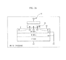
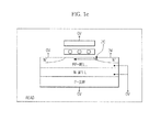
- FIGS. 1A to 1C are drawings to describe the operation of the flash memory.
- the flash memory is operated by three operations of ERASE, WRITE or PROGRAM or READ.
- the ERASE operation of the flash memory is performed in block units, and represents the changing of a cell from 0 to 1.
- a voltage of 20V is applied at a substrate (12), the electrons at a floating gate are moved toward a lower direction thereof by the F-N Tunneling effect (14).
- the WRITE that is, PROGRAM, operation of the flash memory represents the changing of the cell from 1 to 0 while performing such in byte or page units.
- FIG. 1B when a voltage of 19V is applied to the gate of each cell (16), the electrons are moved in a direction toward the floating gate (18). At this time, the state of the cell becomes the state of OFF Tr, and thus becomes the state of Vt (+).
- the WRITE operation is not being completed on a single occasion, but performs the PROGRAM of the desired data by increasing the voltage value in multiple stages.
- the READ operation of the flash memory is referred to as the operation (20) that is configured to check whether the state of the cell is ON Tr or OFF Tr, and outputs the data as 1 or 0.
- the cell at the flash memory is applied with a stress increasing in the order of ERASE, WRITE, and READ, and after a particular level of the stress is applied, the flash memory is reached to a level at which the flash memory is no longer usable, and as such is referred to as the state of WEAR-OUT of the flash memory.
- the flash memory due to the unique features thereof, may be provided with bit errors occurred therein, and the detecting and correcting the error are needed.
- an error correcting code ECC
- ECC error correcting code
- REWRITE may be possible to the flash memory without having to erase the 0xff data that is recorded, but if an ECC generated with respect to the 0xff data is not an 0xff ECC, a corresponding block is needed to be erased in order to perform the REWRITE to the flash memory.
- a frequent 'erase' operation with respect to the flash memory reduces the lifespan of the flash memory and the recording performance of the flash memory.
- a memory system including a flash memory and a memory controller configured to control an operation to record data on the flash memory or to reproduce the recorded data from the flash memory.
- the memory controller may include an encoder, a memory interface and a decoder.
- the encoder may be configured to generate an Error Correction Code (ECC) from data that is to be recorded in the flash memory and to convert the generated ECC by using a particular ECC.
- the memory interface may be configured to record the data and the converted ECC to the flash memory.
- the decoder may be configured to restore the converted ECC, which is read from the flash memory, by using the particular ECC and to detect and correct an error of the data, which t is read from the flash memory, by using the restored ECC.
- the particular ECC may be an ECC with respect to 0xff data.
- the encoder may include an ECC generating unit configured to generate an ECC from input data that is to be recorded in the flash memory, and an ECC converting unit configured to convert the generated ECC by using the particular ECC.
- the decoder may include an ECC restoring unit configured to restore the converted ECC, which is read from the flash memory, by using the particular ECC, and an error detecting/correcting unit configured to detect and correct an error of the data, which is read from the flash memory, by using the restored ECC.
- the decoder may further include an ECC generating unit configured to generate an ECC from the recorded data that is read from the flash memory, and a comparison unit configured to compare the ECC generated from the recorded data with the restored ECC.
- the error detecting/correcting unit may detect and correct an error of the data, which is read from the flash memory, by using the ECC generated from the recorded data and the restored ECC.
- the flash memory may be one of a NAND flash memory, a NOR flash memory, and a Magnetic Random Access Memory (MRAM).
- MRAM Magnetic Random Access Memory
- a memory system includes a flash memory and a memory controller that is configured to control an operation to record data on the flash memory or to reproduce the recorded data from the flash memory.
- the memory controller may include an encoder, a memory interface and a decoder.
- the encoder may be configured to generate an Error Correction Code (ECC) from data that is to be recorded in the flash memory and to convert the generated ECC by using a particular ECC.
- the memory interface may be configured to record the data and the converted ECC to the flash memory ECC.
- the decoder may be configured to restore converted ECC, which is read from the flash memory, by using the particular ECC and to detect and correct an error of the data, which is read from the flash memory, by using the restored ECC.
- the flash memory may include a data region and a spare region. The data may be stored in the data region and the converted ECC may be stored in the spare region.
- the particular ECC may be an ECC with respect to 0xff data.
- a method for recording/reproducing data of a memory system having a flash memory is as follows.
- Data may be recorded in the flash memory.
- An ECC may be generated from the recorded data.
- the generated ECC may be converted by using a particular ECC.
- the converted ECC may be converted to the flash memory.
- the recorded data may be read from the flash memory.
- An ECC may be generated from the recorded data that is read from the flash memory.
- the converted ECC may be read from the flash memory.
- the converted ECC may be restored by using the particular ECC.
- An error of the recorded data, which is read from the flash memory may be detected and corrected by using the restored ECC.
- the particular ECC may be an ECC with respect to 0xff data.
- the method may further include comparing the ECC generated from the recorded data with the restored ECC.
- the detecting and correcting of an error of the recorded data, which is read, may be performed when the ECC generated from the recorded data is not identical to the restored ECC as a result of a comparison.
- the flash memory may be one of a NAND flash memory, a NOR flash memory, and a Magnetic Random Access Memory (MRAM).
- MRAM Magnetic Random Access Memory
- the flash memory may include a data region and a spare region, and the data may be stored in the data region and the converted ECC may be stored in the spare region.
- a method for recording/reproducing data of a memory system having a flash memory the method is as follows.
- Data may be recorded in the flash memory.
- An ECC may be generated from the recorded data.
- the generated ECC may be converted by using a particular ECC.
- the converted ECC may be recorded to the flash memory.
- the particular ECC may be an ECC with respect to 0xff data.
- the flash memory may include a data region and a spare region, and the data may be stored in the data region and the converted ECC may be stored in the spare region.
- a method for recording/reproducing data of a memory system having a flash memory the method is as follows.
- a recorded data may be read from the flash memory.
- An ECC may be generated from the recorded data that is read from the flash memory.
- the converted ECC may be read from the flash memory.
- the converted ECC may be restored by using a particular ECC.
- An error of the recorded data, which is read from the flash memory, may be detected and corrected by using the restored ECC.
- the particular ECC may be an ECC with respect to 0xff data.
- the method may further include comparing the ECC generated from the recorded data with the restored ECC.
- the detecting and correcting of an error of the recorded data, which is read from the flash memory, may be performed when the ECC generated from the recorded data is not identical to the restored ECC as a result of a comparison.
- the lifespan of the flash memory may be extended while enhancing a recording performance of the flash memory.
- 0xff ECC with respect to 0xff data may be generated.
- FIG. 2 is a control block diagram of a memory system in accordance with an embodiment of the present disclosure.
- a memory system in accordance with an embodiment of the present disclosure includes a memory controller 200 and a flash memory 300.
- the flash memory 300 is configured to operate according to the control of the main controller 200, and to store M-bit data information per cell.
- the M-bit data information may include 2-bit data, 3-bit data, and 4-bit data, for example.
- the flash memory 300 may be embodied with a NAND flash memory, a NOR flash memory, a Phase Change Random Access Memory (PRAM), a Magnetic Random Access Memory (MRAM), or a non-volatile memory.
- PRAM Phase Change Random Access Memory
- MRAM Magnetic Random Access Memory
- the memory controller 200 by a request of a host 100, is configured to control the flash memory 300.
- the memory controller 200 includes a host interface 210, a memory interface 220, a controller 230, and an ECC controlling device 240.
- the host interface 210 is configured to provide an interface with the host 100
- the memory interface 220 is configured to provide an interface with the flash memory 300.
- the controller 230 may be implemented by a processor that is configured to control an overall operation of the memory controller 200.
- the host 100 and the memory controller 200 are configured in a way to communicate through various communication interfaces such as a Peripheral Component Interconnect (PCI) and a Universal Serial Bus (USB).
- PCI Peripheral Component Interconnect
- USB Universal Serial Bus
- the memory controller 200 and the flash memory 300 are configured in a way to communicate through a widely known method such as a NAND/NOR interface scheme.
- the memory system that includes the memory controller 200 and the flash memory 300 may be a memory card such as a flash memory card and a smart card.
- the ECC controlling device 240 by using an algorithm of a particular ECC, generates an Error Correction Code (ECC) with respect to data that is to be stored in the flash memory 300.
- ECC Error Correction Code
- the ECC is used for detecting and/or correcting an error.
- the ECC controlling device 240 performs the detection and correction of the error with respect to the data that is read from the flash memory 300.
- the ECC controlling device 240 at an inside of the memory system of an embodiment of the present disclosure generates an ECC from data that is to be recorded to the flash memory 300, and converts the generated ECC by using a particular ECC.
- the data, which is desired to be stored by a user, and the converted ECC, both of which are intended to be stored by a user, are stored in the flash memory 300.
- the ECC controlling device 240 by using the particular ECC, restores the converted ECC, which is read from the flash memory 300, by the particular ECC, and detects/corrects an error of the data, which is read from the flash memory 300, by using the restored ECC.
- the ECC controlling device 240 in accordance with an embodiment of the present disclosure includes an ECC encoder 250 configured to generate an ECC from the data, which is to be recorded, and to convert the generated ECC by using the particular ECC and a decoder 260 configured to restore the converted ECC, which is read from the flash memory 300, by using the particular ECC, and to detect and correct the error of the data that is read from the flash memory 300 by using the restored ECC.
- the particular ECC represents an ECC with respect to 0xff data.
- the ECC controlling device 240 generates an ECC from the data that is to be recorded to the flash memory 300, and converts the ECC, which is generated from the data that is to be recorded, through an exclusive OR (XOR) of the generated ECC and an ECC for 0xff data generated by using an ECC algorithm being used at the memory system.
- the ECC controlling device 240 is configured to restore the ECC, which is converted at the process of recording the data, through an exclusive OR (XOR) of the converted ECC, which is converted and stored at the process of recording the data, and an ECC, which is related to 0xff data generated by using the ECC algorithm being used at the memory system. Then, an error of the data read from the flash memory 300 is detected and corrected by using the restored ECC.
- the ECC controlling device 240 at an inside the memory system in accordance with an embodiment of the present disclosure converts the ECC, which generated from the data that is to be recorded, through the exclusive OR (XOR) of the generated ECC and the ECC which corresponds to 0xff data.
- the ECC controlling device 240 restores the converted ECC through the exclusive OR (XOR) of the converted ECC and the ECC with respect to 0xff data.
- FIG. 3 is a drawing showing the structure of an ECC controlling device illustrated on FIG. 2 .
- the ECC controlling device 240 includes the ECC encoder 250 and the ECC decoder 260.
- the ECC encoder 250 includes an ECC generating unit 252 to generate an ECC with respect to data that is to be stored at the flash memory 300, and an ECC converting unit 254 to convert the ECC, which is generated through the ECC generating unit 252, by using a particular ECC, that is, an ECC with respect to 0xff data.
- the ECC generating unit 252 generates an ECC with respect to data, which is to be recorded, by receiving program data (IN_DATA) and using a particular ECC algorithm.
- the ECC generating unit 252 is configured to generate a linear code as an ECC, and some of the examples of the linear code may include repetition codes, parity codes, cyclic codes, Hamming code, Golay code, RS code (Reed-Solomoncodes), BCH code (Bose, Ray-Chaudhuri, Hocquenghem), and RM codes (Reed-Muller codes).
- the ECC converting unit 254 is input with the generated ECC from the ECC generating unit 252, and uses Mathematical Formula 1 below, thereby converting the generated ECC.
- Converted ECC Generated ECC XOR ECC with respect to 0 ⁇ xff data
- the converted ECC which is output from the ECC converting unit 254, is added to the program data (IN_DATA) that is input from the host 100, and is stored at the flash memory 300 through the memory interface 220.
- the ECC decoder 260 includes an ECC generating unit 262, an ECC restoring unit 264, a comparison unit 266 and an error detecting/correcting unit 268.
- the ECC generating unit 262 generates an ECC from the recorded data that is read from the flash memory 300.
- the ECC restoring unit 264 restores the ECC, which is converted at a process of recording the data and stored, by using a particular ECC (ECC with respect to 0xff data).
- the comparison unit 266 compares the ECC generated through the ECC generating unit 262 with the ECC restored through the ECC restoring unit 264.
- the error detecting/correcting unit 268 detects/corrects the error of the data, which is read from the flash memory 300, by using the restored ECC and the ECC generated through the ECC generating unit 262 according to the result of a comparison of the comparison unit 266.
- the ECC generating unit 262 is input with data, that is, main data among read data (R-DATA) including the main data and the converted ECC, and generates an ECC, which is with respect to data that is to be reproduced, by using the same algorithm as the ECC algorithm that has been used in the recording process of the data.
- the ECC restoring unit 264 is input with the converted ECC from the read data (R_DATA), and restores the converted ECC by using Mathematical Formula 2 below.
- Restored ECC Converted ECC XOR ECC with respect to 0 ⁇ xff data
- the comparison unit 266 determines whether the ECC generated through the ECC generating unit 262 is identical to the restored ECC restored through the ECC restoring unit 264, and outputs the result of the determination to the error detecting/correcting unit 268.
- FIG. 4 is a drawing to describe the data format of the data recorded in the flash memory and the data read from the flash memory.
- FIG. 4 shows the format of a write data (W_DATA) and the read data (R_DATA) that are respectively stored in and read from the flash memory 300 illustrated on FIG. 3 .
- the flash memory 300 includes a memory cell array that including at least two storage region.
- the first storage region is referred to a data region 410 at which (main) data that is transmitted from a host 100 is stored
- the second storage region is referred to a spare region 420 at which basic information, which is supplementary, such as an ECC for stored in the data region 410, is stored.
- the (main) data that is transmitted from the host 100 is stored in the data region 410
- the ECC in detail, a converted ECC with respect to the (main) data is stored in the spare region 420.
- FIG. 5 is a flow chart illustrating a method for recording data of a memory system in accordance with an embodiment of the present disclosure.
- the memory interface 220 records the data to the data region 410 of the flash memory 300 (510).
- the ECC generating unit 252 at an inside the ECC encoder 250 generates the ECC that is related to the data, which is being recorded at the flash memory 300, by using a particular algorithm (520).
- the ECC converting unit 254 at an inside the ECC encoder 250 by using the particular ECC, that is, an ECC with respect to 0xff data, converts the ECC that is generated through the ECC generating unit 252 (530).
- the converted ECC is calculated by using Formula 1 below.
- Converted ECC Generated ECC XOR ECC with respect to 0 ⁇ xff data
- the memory interface 220 After the converted ECC is calculated through the ECC converting unit 254, the memory interface 220 records the converted ECC to the spare region 420 of the flash memory 300 (540).
- the recording process on the flash memory 300 is completed, and the flash memory 300 is provided with the write data (W_DATA) recorded thereto, and the write data (W_DATA) includes the program data and the converted ECC that is generated by the ECC converting unit 254.
- FIG. 6 is a flow chart illustrating a method for reproducing data of a memory system in accordance with an embodiment of the present disclosure.
- the ECC decoder 260 reads the recorded data from the flash memory 300 (610). At this time, the read data (R_DATA) includes the program data and the converted ECC, which is generated through the ECC converting unit 254 at the time at the writing process.
- the ECC generating unit 262 at an inside the ECC decoder 260 is input with the (main) data of the read data (R_DATA), and generates an ECC with respect to data, which is to be reproduced, by using the same algorithm as the ECC algorithm used in the recording process of the data (620).
- the ECC decoder 260 reads the ECC, which is converted and stored at the recording process, from the flash memory 300 (630).
- the ECC restoring unit 264 at an inside the ECC decoder 260 by using the particular ECC, that is, the ECC with respect to 0xff data, restores the ECC that is converted in the recording process (640).
- the restored ECC is calculated by using Formula 2 below.
- Restored ECC Converted ECC XOR ECC with respect to 0 ⁇ xff data
- the comparison unit 266 at an inside the ECC decoder 260 determines whether the ECC generated through the ECC generating unit 262 and the ECC restored through the ECC restoring unit 264 are the same (650). If the ECC generated through the ECC generating unit 262 and the ECC restored through the ECC restoring unit 264 are not the same, that is, if determined as 'NO' in operation 650, the error detecting/correcting unit 268, by using the ECC generated through the ECC generating unit 262 and the restored ECC, detects/corrects the error of the data that is read from the flash memory 300. The data having the error thereof corrected through the detecting/correcting unit 268 is transmitted to the host 100 through the host interface 210.
- the ECC decoder 260 transmits the data, which is read from the flash memory 300, to the host 100 through the host interface 210.
Landscapes
- Engineering & Computer Science (AREA)
- Theoretical Computer Science (AREA)
- Quality & Reliability (AREA)
- Physics & Mathematics (AREA)
- General Engineering & Computer Science (AREA)
- General Physics & Mathematics (AREA)
- Techniques For Improving Reliability Of Storages (AREA)
- Read Only Memory (AREA)
Applications Claiming Priority (1)
| Application Number | Priority Date | Filing Date | Title |
|---|---|---|---|
| KR1020110108886A KR20130044694A (ko) | 2011-10-24 | 2011-10-24 | 메모리 시스템 및 그 데이터 기록 재생 방법 |
Publications (2)
| Publication Number | Publication Date |
|---|---|
| EP2587377A2 true EP2587377A2 (de) | 2013-05-01 |
| EP2587377A3 EP2587377A3 (de) | 2015-02-25 |
Family
ID=47522237
Family Applications (1)
| Application Number | Title | Priority Date | Filing Date |
|---|---|---|---|
| EP12188823.4A Withdrawn EP2587377A3 (de) | 2011-10-24 | 2012-10-17 | Speichersystem und Verfahren zur Aufzeichnung/Wiedergabe von Daten davon |
Country Status (4)
| Country | Link |
|---|---|
| US (1) | US20130104003A1 (de) |
| EP (1) | EP2587377A3 (de) |
| KR (1) | KR20130044694A (de) |
| CN (1) | CN103065683A (de) |
Families Citing this family (5)
| Publication number | Priority date | Publication date | Assignee | Title |
|---|---|---|---|---|
| US9274882B2 (en) * | 2013-12-04 | 2016-03-01 | International Business Machines Corporation | Page retirement in a NAND flash memory system |
| KR102324769B1 (ko) | 2015-06-29 | 2021-11-10 | 삼성전자주식회사 | 반도체 메모리 장치의 에러 정정 회로, 반도체 메모리 장치 및 이를 포함하는 메모리 시스템 |
| KR102692669B1 (ko) * | 2016-02-16 | 2024-08-07 | 삼성전자주식회사 | 메모리의 특성을 이용한 키 생성 방법 및 장치 |
| CN108564983A (zh) * | 2018-04-10 | 2018-09-21 | 南京扬贺扬微电子科技有限公司 | 一种用于nand flash的ldpc测试平台 |
| WO2022120586A1 (zh) * | 2020-12-08 | 2022-06-16 | 华为技术有限公司 | 一种存储装置、存储控制装置及片上系统 |
Family Cites Families (11)
| Publication number | Priority date | Publication date | Assignee | Title |
|---|---|---|---|---|
| JP2002175090A (ja) * | 2000-12-07 | 2002-06-21 | Sony Corp | 再生装置および再生方法 |
| US20030135798A1 (en) * | 2001-12-13 | 2003-07-17 | Yukari Katayama | Optical disk device and data randomizing method for optical disk device |
| KR100643288B1 (ko) * | 2004-11-16 | 2006-11-10 | 삼성전자주식회사 | 플래시 메모리의 데이터 처리 장치 및 방법 |
| KR100842680B1 (ko) * | 2007-01-08 | 2008-07-01 | 삼성전자주식회사 | 플래시 메모리 장치의 오류 정정 컨트롤러 및 그것을포함하는 메모리 시스템 |
| TWI332611B (en) * | 2007-05-24 | 2010-11-01 | Realtek Semiconductor Corp | Method for writing data in flash memory and error correction coding/decoding method thereof |
| US8145977B2 (en) * | 2007-10-15 | 2012-03-27 | Joseph Schweiray Lee | Methods and apparatus for providing error correction to unwritten pages and for identifying unwritten pages in flash memory |
| US8555143B2 (en) * | 2008-12-22 | 2013-10-08 | Industrial Technology Research Institute | Flash memory controller and the method thereof |
| TWI465898B (zh) * | 2009-07-13 | 2014-12-21 | Silicon Motion Inc | 避免資料儲存裝置之資料發生移位錯誤的方法及控制器 |
| US20110040924A1 (en) * | 2009-08-11 | 2011-02-17 | Selinger Robert D | Controller and Method for Detecting a Transmission Error Over a NAND Interface Using Error Detection Code |
| TWI438777B (zh) * | 2010-06-10 | 2014-05-21 | Global Unichip Corp | 一種快閃記憶體控制器之資料傳輸保護裝置 |
| JP5269936B2 (ja) * | 2011-03-17 | 2013-08-21 | 株式会社東芝 | 符号化器及び記憶装置 |
-
2011
- 2011-10-24 KR KR1020110108886A patent/KR20130044694A/ko not_active Withdrawn
-
2012
- 2012-10-11 US US13/649,337 patent/US20130104003A1/en not_active Abandoned
- 2012-10-17 EP EP12188823.4A patent/EP2587377A3/de not_active Withdrawn
- 2012-10-24 CN CN2012104085724A patent/CN103065683A/zh active Pending
Non-Patent Citations (1)
| Title |
|---|
| None |
Also Published As
| Publication number | Publication date |
|---|---|
| KR20130044694A (ko) | 2013-05-03 |
| CN103065683A (zh) | 2013-04-24 |
| US20130104003A1 (en) | 2013-04-25 |
| EP2587377A3 (de) | 2015-02-25 |
Similar Documents
| Publication | Publication Date | Title |
|---|---|---|
| KR100842680B1 (ko) | 플래시 메모리 장치의 오류 정정 컨트롤러 및 그것을포함하는 메모리 시스템 | |
| CN101256842B (zh) | 纠错码控制器和包括该纠错码控制器的存储器系统 | |
| KR102677592B1 (ko) | 연장된 제품 수명을 갖는 메모리장치 및 그 동작방법 | |
| KR101616100B1 (ko) | 메모리 시스템 및 그것의 동작 방법 | |
| US8650463B2 (en) | Solid state drive and method of controlling an error thereof | |
| US20100269000A1 (en) | Methods and apparatuses for managing bad memory cell | |
| US8732553B2 (en) | Memory system and control method thereof | |
| US9411679B2 (en) | Code modulation encoder and decoder, memory controller including them, and flash memory system | |
| US8448043B2 (en) | Overwritable nonvolatile memory device and related data write method | |
| US20160350179A1 (en) | Decoding method, memory storage device and memory control circuit unit | |
| US9147483B2 (en) | Apparatus and method of operating memory device | |
| US20100100763A1 (en) | Flash memory controller having configuring unit for error correction code (ecc) capability and method thereof | |
| CN103680637A (zh) | 具有异常字线检测器的闪存系统及其异常字线检测方法 | |
| WO2014164134A2 (en) | Detecting effect of corrupting event on preloaded data in non-volatile memory | |
| MX2012010944A (es) | Detección de distribución de paridad no regulada vía etiqueta de metadatos. | |
| TW201346923A (zh) | 使用單一錯誤偵測奇偶校驗的抹除修正 | |
| US20140136925A1 (en) | Method of operating a data storage device | |
| US8347183B2 (en) | Flash memory device using ECC algorithm and method of operating the same | |
| KR20130027138A (ko) | 에러 정정 방법 및 이를 이용하는 메모리 장치 | |
| US7613982B2 (en) | Data processing apparatus and method for flash memory | |
| US12038805B1 (en) | Hard error tracker and HRR dynamic reordering | |
| US20100287448A1 (en) | Flash memory device with rectifiable redundancy bit and method of controlling the same | |
| EP2587377A2 (de) | Speichersystem und Verfahren zur Aufzeichnung/Wiedergabe von Daten davon | |
| KR102866396B1 (ko) | 비휘발성 메모리의 불량 행 관리를 수행하는 메모리 시스템 및 이의 동작 방법 | |
| CN112051963A (zh) | 数据写入方法、存储器控制电路单元以及存储器存储装置 |
Legal Events
| Date | Code | Title | Description |
|---|---|---|---|
| PUAI | Public reference made under article 153(3) epc to a published international application that has entered the european phase |
Free format text: ORIGINAL CODE: 0009012 |
|
| AK | Designated contracting states |
Kind code of ref document: A2 Designated state(s): AL AT BE BG CH CY CZ DE DK EE ES FI FR GB GR HR HU IE IS IT LI LT LU LV MC MK MT NL NO PL PT RO RS SE SI SK SM TR |
|
| AX | Request for extension of the european patent |
Extension state: BA ME |
|
| PUAL | Search report despatched |
Free format text: ORIGINAL CODE: 0009013 |
|
| AK | Designated contracting states |
Kind code of ref document: A3 Designated state(s): AL AT BE BG CH CY CZ DE DK EE ES FI FR GB GR HR HU IE IS IT LI LT LU LV MC MK MT NL NO PL PT RO RS SE SI SK SM TR |
|
| AX | Request for extension of the european patent |
Extension state: BA ME |
|
| RIC1 | Information provided on ipc code assigned before grant |
Ipc: G06F 11/10 20060101AFI20150120BHEP |
|
| STAA | Information on the status of an ep patent application or granted ep patent |
Free format text: STATUS: THE APPLICATION IS DEEMED TO BE WITHDRAWN |
|
| 18D | Application deemed to be withdrawn |
Effective date: 20150826 |