EP2579298A1 - Heat-treatment furnace - Google Patents
Heat-treatment furnace Download PDFInfo
- Publication number
- EP2579298A1 EP2579298A1 EP11789911.2A EP11789911A EP2579298A1 EP 2579298 A1 EP2579298 A1 EP 2579298A1 EP 11789911 A EP11789911 A EP 11789911A EP 2579298 A1 EP2579298 A1 EP 2579298A1
- Authority
- EP
- European Patent Office
- Prior art keywords
- heat
- core tube
- treatment
- furnace
- boat
- Prior art date
- Legal status (The legal status is an assumption and is not a legal conclusion. Google has not performed a legal analysis and makes no representation as to the accuracy of the status listed.)
- Granted
Links
Images


Classifications
-
- H—ELECTRICITY
- H10—SEMICONDUCTOR DEVICES; ELECTRIC SOLID-STATE DEVICES NOT OTHERWISE PROVIDED FOR
- H10P—GENERIC PROCESSES OR APPARATUS FOR THE MANUFACTURE OR TREATMENT OF DEVICES COVERED BY CLASS H10
- H10P95/00—Generic processes or apparatus for manufacture or treatments not covered by the other groups of this subclass
- H10P95/90—Thermal treatments, e.g. annealing or sintering
-
- H—ELECTRICITY
- H10—SEMICONDUCTOR DEVICES; ELECTRIC SOLID-STATE DEVICES NOT OTHERWISE PROVIDED FOR
- H10P—GENERIC PROCESSES OR APPARATUS FOR THE MANUFACTURE OR TREATMENT OF DEVICES COVERED BY CLASS H10
- H10P32/00—Diffusion of dopants within, into or out of wafers, substrates or parts of devices
-
- H—ELECTRICITY
- H10—SEMICONDUCTOR DEVICES; ELECTRIC SOLID-STATE DEVICES NOT OTHERWISE PROVIDED FOR
- H10P—GENERIC PROCESSES OR APPARATUS FOR THE MANUFACTURE OR TREATMENT OF DEVICES COVERED BY CLASS H10
- H10P72/00—Handling or holding of wafers, substrates or devices during manufacture or treatment thereof
- H10P72/04—Apparatus for manufacture or treatment
- H10P72/0431—Apparatus for thermal treatment
- H10P72/0434—Apparatus for thermal treatment mainly by convection
-
- H—ELECTRICITY
- H10—SEMICONDUCTOR DEVICES; ELECTRIC SOLID-STATE DEVICES NOT OTHERWISE PROVIDED FOR
- H10P—GENERIC PROCESSES OR APPARATUS FOR THE MANUFACTURE OR TREATMENT OF DEVICES COVERED BY CLASS H10
- H10P72/00—Handling or holding of wafers, substrates or devices during manufacture or treatment thereof
- H10P72/30—Handling or holding of wafers, substrates or devices during manufacture or treatment thereof for conveying, e.g. between different workstations
- H10P72/33—Handling or holding of wafers, substrates or devices during manufacture or treatment thereof for conveying, e.g. between different workstations into and out of processing chamber
- H10P72/3311—Horizontal transfer of a batch of workpieces
Definitions
- This invention relates to a heat-treatment furnace for use in the heat treatment of semiconductor substrates, typically silicon substrates.
- a semiconductor heat treating process is generally carried out in a furnace of the following design in order to prevent any contamination from the ambient air, heater or the like.
- a furnace core tube 21 of high-purity quartz or the like which is provided with an opening 22 at one end and a gas inlet conduit 23 at the other end is disposed inside a cylindrical heater 24 which is previously installed in the furnace.
- a boat 26 of high-purity quartz or the like having semiconductor substrates 25 rested thereon is moved into the furnace core tube 21 through the opening 22 and set in place.
- a lid 27 of high-purity quartz or the like is closed to establish a substantially tight seal.
- High-purity gas such as nitrogen or argon is fed from the gas inlet conduit 23 whereas the gas is discharged out of the furnace through small gaps between the core tube 21 and the lid 27. While the in-furnace atmosphere is kept clean in this way, heat treatment for dopant diffusion or oxidation is carried out.
- FIG. 7 illustrates one exemplary heat-treatment flow using a heat-treatment furnace including such a core tube
- FIG. 10 illustrates one exemplary time sequence of the heat treatment.
- the prior art heat treating process is described by referring to these figures.
- the semiconductor substrates must be cooled at the boat station until a handleable temperature is reached.
- the system remains unready for insertion of a next batch, introducing a standby time between consecutive heat treatment batches.
- the heat-treatment furnace is described therein as comprising a furnace core tube which is open at one end, a shutter for operatively closing the open end, and a partition disposed in the core tube and inside the open end so as to define a gap between the partition and the inner wall of the core tube, the shutter being provided with a vent.
- This design allegedly eliminates any adverse impact by entry of ambient air.
- the semiconductor substrates In the heat-treatment furnace comprising a core tube of the above-mentioned structure, however, semiconductor substrates must be moved into and out of the furnace via only one end of the core tube because of the structure. Furthermore, as indicated above, the semiconductor substrates after being taken out of the hot furnace must be cooled at the boat station until a handleable temperature is reached. For continuous implementation of the heat treatment, this introduces a standby time between consecutive heat treatment batches. Particularly when semiconductor devices which are subject to a relatively short duration of heat treatment, typically crystalline silicon solar cells, are heat treated, the standby time accounts for a relatively high proportion among the overall heat treatment time, which becomes the major cause of restricting the productivity of the heat treatment process.
- the furnace has low gas tightness due to the presence of the belt or beam, even in the structure provided with shutters at the inlet and outlet, and fails to prevent inflow of ambient air, giving rise to a problem that the carrier lifetime of semiconductor substrates can be significantly reduced by the heat treatment.
- Such continuous mode heat treatment furnaces of the belt conveyor or walking beam system also have problems including a small number of simultaneously processable workpieces per unit area, and low thermal efficiency.
- An object of the invention which has been made under the above-mentioned circumstances, is to provide a heat-treatment furnace which is adapted to reduce a standby time between batches during consecutive heat treatment of semiconductor substrates for thereby improving productivity and to reduce the frequency of breaking of gas inlet conduits for thereby saving the running cost of the heat-treatment process.
- a furnace core tube for use in heat treatment process is structured as a cylindrical shape tube which is provided at opposite ends with openings having a sufficient size to allow semiconductor substrates to be moved into and out of the core tube, a lid is detachably mounted to the core tube to block each opening to substantially seal the core tube, the core tube or lid is provided with a thin gas inlet conduit for introducing gas into the core tube, whereby the atmosphere within the furnace can be kept clean during heat treatment, and the semiconductor substrates may be moved into and out of the core tube and heat treated therein while the lids at opposite ends are opened and closed as necessary, whereby a standby time between batches during consecutive heat treatment can be reduced for thereby improving productivity.
- the core tube is structured as a simple cylindrical shape, the frequency of breaking of gas inlet conduits is reduced and the cost of the core tube itself is reduced. As a result, the running cost of the heat-treatment process can be saved.
- the invention is predicated on these findings.
- the invention provides a heat-treatment furnace as defined below.
- the invention reduces a standby time between batches during consecutive heat treatment of semiconductor substrates, thereby improving productivity.
- the core tube structured as a simple cylindrical shape reduces the frequency of breaking of gas inlet conduits, thereby saving the running cost of the heat-treatment process.
- FIG. 1 illustrates the structure of one exemplary core tube included in the heat-treatment furnace of the invention.
- a cylindrical core tube 1 has openings 2a, 2b at axially or longitudinally opposite ends and is concentrically enclosed by a cylindrical heater 4 which is installed in a heat-treatment furnace (not shown).
- a boat 6 on which semiconductor substrates 5 are rested may be moved into and out of the core tube through either one of the openings 2a, 2b.
- the openings 2a, 2b may be substantially blocked and sealed by lids 7a, 7b, respectively.
- the lids 7a, 7b are integrally provided with thin gas inlet conduits 8a, 8b which penetrate through the lids 7a, 7b in a gas-tight manner for introducing gas into the core tube.
- gas inlet conduits 8a, 8b With the lids 7a, 7b closed, gas can be fed from the selected one of gas inlet conduits 8a, 8b.
- the gas inlet conduits 8a, 8b need not necessarily be integrated with the lids 7a, 7b or protruded from the lids 7a, 7b.
- a separate structure is acceptable which consists of bores in the lids 7a, 7b and gas inlet conduits such that the conduit may be fixedly engaged in the bore by snug fit.
- FIG. 2 illustrates the structure of another exemplary core tube included in the heat-treatment furnace of the invention.
- a cylindrical core tube 1' has openings 2a, 2b at axially or longitudinally opposite ends and thin gas inlet conduits 9a, 9b disposed near the opposite ends and at the lower side.
- the core tube 1' is concentrically enclosed by a cylindrical heater 4 which is installed in a heat-treatment furnace (not shown).
- a boat 6 on which semiconductor substrates 5 are rested may be moved into and out of the core tube through either one of the openings 2a, 2b.
- the openings 2a, 2b may be substantially blocked and sealed by lids 7a, 7b, respectively.
- gas inlet conduits 9a, 9b With the lids 7a, 7b closed, gas can be fed from the selected one of gas inlet conduits 9a, 9b.
- the gas inlet conduits 9a, 9b need not necessarily be integrated with or protruded from the core tube 1'.
- a separate structure is acceptable which consists of bores and gas inlet conduits such that the conduit may be fixedly engaged in the bore by snug fit.
- FIG. 3 illustrates the structure of a further exemplary core tube included in the heat-treatment furnace of the invention.
- a cylindrical core tube 1" has openings 2a, 2b at axially or longitudinally opposite ends and a gas inlet conduit 8c disposed near the longitudinal center and at the upper side.
- the core tube 1" is concentrically enclosed by a cylindrical heater 4 which is installed in a heat-treatment furnace (not shown).
- a boat 6 on which semiconductor substrates 5 are rested may be moved into and out of the core tube through either one of the openings 2a, 2b.
- the openings 2a, 2b may be substantially blocked and sealed by lids 7a, 7b, respectively.
- the lids 7a, 7b are integrally provided with thin gas inlet conduits 8a, 8b which penetrate through the lids 7a, 7b in a gas-tight manner for introducing gas into the core tube. With the lids 7a, 7b closed, gas can be fed from the selected one of gas inlet conduits 8a, 8b, 8c. If gas is fed into the core tube from the gas inlet conduit 8c with the lids 7a, 7b kept open, then the gas may flow toward the openings 2a, 2b.
- the gas inlet conduits 8a, 8b, 8c need not necessarily be integrated with or protruded from the lids 7a, 7b or core tube 1".
- a separate structure is acceptable which consists of bores and gas inlet conduits such that the conduit may be fixedly engaged in the bore by snug fit.
- the core tube, lids, and gas inlet conduits used herein are typically made of high-purity quartz, high-purity silicon carbide (SiC) or similar material in order that the components are resistant to the high temperature of heat treatment and can keep the furnace interior clean.
- SiC silicon carbide
- the size of the core tube is not particularly limited.
- the inner diameter of the openings at opposite ends of the core tube may be sized so as to allow the semiconductor substrate-carrying boat to be moved into and out of the core tube, and is preferably at least 95% of the inner diameter of the core tube at the center, and typically equal to the inner diameter of the core tube at the center.
- the gas inlet conduits have an outer diameter of preferably 5 to 25 mm, more preferably 10 to 20 mm, an inner diameter of preferably 3 to 20 mm, more preferably 5 to 15 mm, and a protrusion length of preferably 50 to 200 mm, more preferably 100 to 150 mm.
- the gas inlet conduits are preferably spaced inward a distance of 10 to 200 mm, more preferably 20 to 150 mm from the openings.
- At least one boat station is preferably provided outside the core tube and in proximity to the opening where the boat 6 having substrates 5 rested thereon is on standby. More preferably at least one boat station is provided at a predetermined distance from each opening.
- the boat station may be made of the same material as the core tube, lids, and gas inlet conduits.
- the size of the boat station is not particularly limited as long as it allows the boat to stand by. For example, a boat station having a wall thickness of 4 mm, a length of 1,000 mm, and a width of 200 mm and defining an arcuate curved surface with a radius of 100 mm and an angle of 60° may be used.
- Semiconductor substrates are heat treated in the heat-treatment furnace comprising a core tube of the structure as shown in FIGS. 1 to 3 .
- a high-purity gas such as argon, nitrogen or oxygen is introduced from the gas inlet conduit while the high-purity gas may escape from the furnace through a small gap between the lid and the core tube.
- the gas flow prevents the ambient air from entering the furnace and keeps the atmosphere in the furnace clean during heat treatment. Then an array of semiconductor substrates on the boat positioned at the center of the core tube can be heat treated without a substantial loss of the carrier lifetime of the semiconductor substrates.
- FIG. 5 illustrates an exemplary heat-treatment flow using a heat-treatment furnace comprising a core tube according to the invention and FIG. 8 illustrates a time sequence of this heat treatment.
- the core tube in FIG. 5 is the same as in FIG. 1 .
- This embodiment including two boat stations has the advantage of reduced standby time in that when the boat is taken out of the core tube and cooled at one boat station 10b, a boat of a next batch may be moved from the other boat station 10a into the core tube. These boats may be moved into and out of the core tube at the same time.
- a rod of high-purity quartz (not shown) may be used in moving the boat into and out of the core tube.
- FIG. 6 illustrates another exemplary heat-treatment flow using a heat-treatment furnace comprising a core tube according to the invention and FIG. 9 illustrates a time sequence of this heat treatment.
- the core tube in FIG. 6 is the same as in FIG. 3 .
- the furnace interior may be kept clean by feeding a high-purity gas such as nitrogen, argon or oxygen from the gas inlet conduit 8c near the longitudinal center of the core tube 1" and discharging the gas through small gaps between the lids 7a, 7b and the openings 2a, 2b at opposite ends of the core tube.
- a high-purity gas such as nitrogen, argon or oxygen
- the standby time may be further reduced by moving the heat treated boat out of and moving a next boat into the core tube at the same time.
- the structure of the heat-treatment furnace accommodating the core tube defined herein is not particularly limited as long as it is a horizontal furnace having a cylindrical heater enclosing the cure tube.
- the heat-treatment furnace of the invention is useful in carrying out the heat treatment of semiconductor substrates and advantageous particularly when the semiconductor substrates are silicon substrates intended for the fabrication of solar cells, specifically for diffusion treatment of p- or n-type dopant into silicon substrates and oxidation treatment of silicon substrates. Besides the dopant diffusion treatment and substrate oxidation treatment, the furnace may be advantageously utilized in any heat treatments which are carried out in a horizontal furnace.
- Lapped boron-doped p-type silicon wafers having a diameter of 100 mm, a thickness of 200 ⁇ m and face orientation (100) prepared by the CZ method (resistivity 1-3 ⁇ -cm) were provided.
- Ten lapped wafers were manually arrayed on a boat of high-purity quartz having a length of 540 mm, a width of 100 mm, and a height of 30 mm, and having 100 channels at a pitch of 2.5 mm.
- the heat-treatment furnace of the invention included, as shown in FIG. 1 , a quartz core tube 1 of outer diameter 150 mm, inner diameter 142 mm, and length 3,000 mm, provided at opposite ends with openings of inner diameter 142 mm, and lids 7a, 7b each comprising a quartz disk of diameter 170 mm and thickness 4 mm, a cylindrical quartz box of outer diameter 141.5 mm and width 50 mm fusion bonded to the disk, and a gas inlet conduit 8a or 8b of inner diameter 5 mm penetrating through the disk and the box.
- boat stations of high-purity quartz each having a wall thickness of 4 mm, a length of 1,000 mm, and a width of 200 mm and defining an arcuate curved surface with a radius of 100 mm and an angle of 60° were provided.
- Each boat station was spaced 250 mm from the opening in the core tube.
- the distance from the boat standby position at the center of the boat station to the heat treatment position at the center of the core tube was 2,250 mm.
- the insertion preparatory time (standby time) taken for setting the boat on the boat station was about 1 minute per batch, and the cooling time after removal of the heat treated boat was 15 minutes per batch.
- a quartz rod having a length of 2,000 mm and an outer diameter of 15 mm and having a boss of 30 mm height protruding perpendicular to the longitudinal direction was provided for moving the boat into and out of the core tube.
- the rod was mounted in a full automatic boat loader whereby the boat was moved into and out of the core tube at a constant speed of 200 mm/min.
- the heat-treatment furnace was normally set at 830°C, and the boat was moved therein. Phosphorus was deposited for 40 minutes and then driven in at 830°C for 17 minutes to effect deeper phosphorus diffusion. Thereafter, the boat was taken out.
- the gas composition for heat treatment was a gas mixture of 20 L/min nitrogen, 0.3 L/min oxygen, and 0.45 L/min phosphorus oxychloride (POCl 3 ) during phosphorus deposition, and a gas mixture of 20 L/min nitrogen and 0.3 L/min oxygen during other steps including standby, lid opening/closing, insertion and removal of the boat, and drive-in. Under these conditions, diffusion heat treatment was carried out in accordance with the heat treatment flow of FIG. 5 and the time sequence of FIG. 8 .
- a quartz core tube of outer diameter 150 mm, inner diameter 142 mm, and length 3,000 mm, having openings of inner diameter 142 mm at opposite ends and a gas inlet conduit of inner diameter 5 mm at a position spaced a distance of 1,500 mm from the longitudinal opposite ends of the core tube as shown in FIG. 3 was provided.
- diffusion heat treatment was carried out in accordance with the heat treatment flow of FIG. 6 and the time sequence of FIG. 9 .
- a conventional quartz core tube of outer diameter 150 mm, inner diameter 142 mm, and length 3,000 mm, having an opening of inner diameter 142 mm at one end and a gas inlet conduit of inner diameter 5 mm at the other end, and a lid comprising a quartz disk of diameter 170 mm and thickness 4 mm and a cylindrical quartz box of outer diameter 141.5 mm and width 50 mm fusion bonded to the disk were provided.
- diffusion heat treatment was carried out in accordance with the heat treatment flow of FIG. 7 and the time sequence of FIG. 10 .
- the substrate was immersed in 25 wt% HF for 4 minutes to remove the glass coating, rinsed with deionized water, and dried.
- the sheet resistance was measured at the wafer center by the four-probe analysis.
- the substrate was immersed in 25 wt% KOH at 70°C for 10 minutes to remove the diffusion layer, rinsed with deionized water, immersed in 1 wt% HF for 1 minute to be water repellent, and subjected to chemical passivation by the iodine methanol method.
- the bulk lifetime was measured by the micro-PCD method.
- Example 1 Comparative Example 1 Average sheet resistance ( ⁇ / ⁇ ) 62.2 62.7 62.4 Average bulk lifetime ( ⁇ sec) 612 603 608 Time per batch of diffusion (min) 67 53 82
- Examples 1 and 2 display measurement results of sheet resistance and bulk lifetime which are comparable to those of Comparative Example 1 while achieving a substantial saving of the time taken per batch of diffusion.
Abstract
Description
- This invention relates to a heat-treatment furnace for use in the heat treatment of semiconductor substrates, typically silicon substrates.
- In the prior art, a semiconductor heat treating process is generally carried out in a furnace of the following design in order to prevent any contamination from the ambient air, heater or the like. As shown in
FIG. 4 , afurnace core tube 21 of high-purity quartz or the like which is provided with an opening 22 at one end and agas inlet conduit 23 at the other end is disposed inside acylindrical heater 24 which is previously installed in the furnace. Aboat 26 of high-purity quartz or the like havingsemiconductor substrates 25 rested thereon is moved into thefurnace core tube 21 through the opening 22 and set in place. Alid 27 of high-purity quartz or the like is closed to establish a substantially tight seal. High-purity gas such as nitrogen or argon is fed from thegas inlet conduit 23 whereas the gas is discharged out of the furnace through small gaps between thecore tube 21 and thelid 27. While the in-furnace atmosphere is kept clean in this way, heat treatment for dopant diffusion or oxidation is carried out. -
FIG. 7 illustrates one exemplary heat-treatment flow using a heat-treatment furnace including such a core tube andFIG. 10 illustrates one exemplary time sequence of the heat treatment. The prior art heat treating process is described by referring to these figures. - (1) A predetermined number of
semiconductor substrates 25 are rested on theboat 26, which is held on standby at aboat station 30. See FIG. 7(a) andFIG. 10 (i) . - (2) The
lid 27 of thecore tube 21 is opened. Theboat 26 havingsemiconductor substrates 25 rested thereon is forcedly moved from theboat station 30 to a predetermined position at the center of the furnace, using a rod of high-purity quartz or the like (not shown). See FIG. 7(a) andFIG. 10 (ii) and (iii) . - (3) The
lid 27 is closed. Thesemiconductor substrates 25 are heat treated according to the predetermined thermal profile. SeeFIG. 7(b) and FIG. 10 (iv). - (4) After the heat treatment, the
lid 27 is opened. Theboat 26 havingsemiconductor substrates 25 rested thereon is forcedly moved from the predetermined position in the furnace to theboat station 30, using a rod or the like, and cooled there. See FIG. 7(c) andFIG. 10 (v) to (vii) . - In this process, after the boat is taken out of the furnace, the semiconductor substrates must be cooled at the boat station until a handleable temperature is reached. When it is desired to continuously carry out a predetermined heat treatment, the system remains unready for insertion of a next batch, introducing a standby time between consecutive heat treatment batches.
- Besides the furnace core tube mentioned above, the structure of a heat treatment furnace for use in the semiconductor substrate heat treating process is proposed, for example, in
JP-A H05-102054 Patent Document 1, Sony Corp., diffusion furnace). The heat-treatment furnace is described therein as comprising a furnace core tube which is open at one end, a shutter for operatively closing the open end, and a partition disposed in the core tube and inside the open end so as to define a gap between the partition and the inner wall of the core tube, the shutter being provided with a vent. This design allegedly eliminates any adverse impact by entry of ambient air. -
- Patent Document 1:
JP-A H05-102054 - In the heat-treatment furnace comprising a core tube of the above-mentioned structure, however, semiconductor substrates must be moved into and out of the furnace via only one end of the core tube because of the structure. Furthermore, as indicated above, the semiconductor substrates after being taken out of the hot furnace must be cooled at the boat station until a handleable temperature is reached. For continuous implementation of the heat treatment, this introduces a standby time between consecutive heat treatment batches. Particularly when semiconductor devices which are subject to a relatively short duration of heat treatment, typically crystalline silicon solar cells, are heat treated, the standby time accounts for a relatively high proportion among the overall heat treatment time, which becomes the major cause of restricting the productivity of the heat treatment process. Also in the case of a furnace core tube of the above-mentioned structure, upon replacement of the furnace core tube for periodic cleaning and shelf storage thereof, a thin tubular gas inlet conduit can be broken. Since the core tube of high-purity quartz or the like is expensive, the expenses for repair and purchase of a new one are high. This is one of the factors that cause to increase the running cost of the heat treatment process.
- Furthermore, when a heat treatment furnace of the continuous mode having inlet and outlet as typified by the belt conveyor or walking beam system is employed, the furnace has low gas tightness due to the presence of the belt or beam, even in the structure provided with shutters at the inlet and outlet, and fails to prevent inflow of ambient air, giving rise to a problem that the carrier lifetime of semiconductor substrates can be significantly reduced by the heat treatment. Such continuous mode heat treatment furnaces of the belt conveyor or walking beam system also have problems including a small number of simultaneously processable workpieces per unit area, and low thermal efficiency.
- An object of the invention, which has been made under the above-mentioned circumstances, is to provide a heat-treatment furnace which is adapted to reduce a standby time between batches during consecutive heat treatment of semiconductor substrates for thereby improving productivity and to reduce the frequency of breaking of gas inlet conduits for thereby saving the running cost of the heat-treatment process.
- Making extensive investigations to attain the above object, the inventors have found that a furnace core tube for use in heat treatment process is structured as a cylindrical shape tube which is provided at opposite ends with openings having a sufficient size to allow semiconductor substrates to be moved into and out of the core tube, a lid is detachably mounted to the core tube to block each opening to substantially seal the core tube, the core tube or lid is provided with a thin gas inlet conduit for introducing gas into the core tube, whereby the atmosphere within the furnace can be kept clean during heat treatment, and the semiconductor substrates may be moved into and out of the core tube and heat treated therein while the lids at opposite ends are opened and closed as necessary, whereby a standby time between batches during consecutive heat treatment can be reduced for thereby improving productivity. Since the core tube is structured as a simple cylindrical shape, the frequency of breaking of gas inlet conduits is reduced and the cost of the core tube itself is reduced. As a result, the running cost of the heat-treatment process can be saved. The invention is predicated on these findings.
- Accordingly, the invention provides a heat-treatment furnace as defined below.
- (1) A heat-treatment furnace for use in the heat treatment of semiconductor substrates, comprising a cylindrical core tube which is provided at opposite ends with openings having a sufficient size to allow semiconductor substrates to be moved into and out of the core tube.
- (2) The heat-treatment furnace of (1), further comprising lids each of which is detachably mounted to the core tube to block the opening to substantially seal the core tube.
- (3) The heat-treatment furnace of (1) or (2), further comprising thin gas inlet conduits penetrating through the lids for introducing gas into the core tube.
- (4) The heat-treatment furnace of any one of (1) to (3), further comprising thin gas inlet conduits disposed near opposite ends of the core tube for introducing gas into the core tube.
- (5) The heat-treatment furnace of any one of (1) to (4), further comprising a thin gas inlet conduit disposed near the longitudinal center of the core tube for introducing gas into the core tube.
- (6) The heat-treatment furnace of any one of (1) to (5), wherein the opening in the core tube has an inner diameter which is at least 95% of the inner diameter of the core tube at the center.
- (7) The heat-treatment furnace of any one of (1) to (6), further comprising at least one boat station disposed outside the core tube and in proximity to the opening in the core tube, the boat station carrying a boat having semiconductor substrates rested thereon on standby.
- (8) The heat-treatment furnace of any one of (1) to (7), wherein the heat treatment is intended to diffuse a p- or n-type dopant into silicon substrates.
- (9) The heat-treatment furnace of any one of (1) to (7), wherein the heat treatment is intended to oxidize silicon substrates.
- The invention reduces a standby time between batches during consecutive heat treatment of semiconductor substrates, thereby improving productivity. The core tube structured as a simple cylindrical shape reduces the frequency of breaking of gas inlet conduits, thereby saving the running cost of the heat-treatment process.
-
-
FIG. 1 is a schematic cross-sectional view of one embodiment of the invention including a furnace core tube and lids having gas inlet conduits. -
FIG. 2 is a schematic cross-sectional view of another embodiment of the invention including a furnace core tube having gas inlet conduits disposed near opposite ends and at the lower side thereof, and lids. -
FIG. 3 is a schematic cross-sectional view of a further embodiment of the invention including a furnace core tube having a gas inlet conduit disposed near the center thereof, and lids. -
FIG. 4 is a schematic cross-sectional view of one exemplary structure of a conventional furnace core tube. -
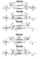
FIG. 5 is a schematic cross-sectional view of a heat-treatment flow using one exemplary heat-treatment furnace of the invention. -
FIG. 6 is a schematic cross-sectional view of a heat-treatment flow using another exemplary heat-treatment furnace of the invention. -
FIG. 7 is a schematic cross-sectional view of a heat-treatment flow using the conventional heat-treatment furnace. -
FIG. 8 illustrates a time sequence of heat treatment using one exemplary heat-treatment furnace of the invention. -
FIG. 9 illustrates a time sequence of heat treatment using another exemplary heat-treatment furnace of the invention. -
FIG. 10 illustrates a time sequence of heat treatment using the conventional heat-treatment furnace. - Embodiments of the invention are described below in detail with reference to the drawings, but the invention is not limited thereto. Throughout the drawings to illustrate the embodiments, parts having the same functions are designated by like numerals and their iterative description is omitted.
-
FIG. 1 illustrates the structure of one exemplary core tube included in the heat-treatment furnace of the invention. InFIG. 1 , acylindrical core tube 1 hasopenings cylindrical heater 4 which is installed in a heat-treatment furnace (not shown). Aboat 6 on whichsemiconductor substrates 5 are rested may be moved into and out of the core tube through either one of theopenings openings lids lids gas inlet conduits lids lids gas inlet conduits gas inlet conduits lids lids lids -
FIG. 2 illustrates the structure of another exemplary core tube included in the heat-treatment furnace of the invention. InFIG. 2 , a cylindrical core tube 1' hasopenings gas inlet conduits cylindrical heater 4 which is installed in a heat-treatment furnace (not shown). Aboat 6 on whichsemiconductor substrates 5 are rested may be moved into and out of the core tube through either one of theopenings openings lids lids gas inlet conduits gas inlet conduits -
FIG. 3 illustrates the structure of a further exemplary core tube included in the heat-treatment furnace of the invention. InFIG. 3 , acylindrical core tube 1" hasopenings gas inlet conduit 8c disposed near the longitudinal center and at the upper side. Thecore tube 1" is concentrically enclosed by acylindrical heater 4 which is installed in a heat-treatment furnace (not shown). Aboat 6 on whichsemiconductor substrates 5 are rested may be moved into and out of the core tube through either one of theopenings openings lids lids gas inlet conduits lids lids gas inlet conduits gas inlet conduit 8c with thelids openings gas inlet conduits lids core tube 1". A separate structure is acceptable which consists of bores and gas inlet conduits such that the conduit may be fixedly engaged in the bore by snug fit. - The core tube, lids, and gas inlet conduits used herein are typically made of high-purity quartz, high-purity silicon carbide (SiC) or similar material in order that the components are resistant to the high temperature of heat treatment and can keep the furnace interior clean.
- The size of the core tube is not particularly limited. The inner diameter of the openings at opposite ends of the core tube may be sized so as to allow the semiconductor substrate-carrying boat to be moved into and out of the core tube, and is preferably at least 95% of the inner diameter of the core tube at the center, and typically equal to the inner diameter of the core tube at the center.
- The gas inlet conduits have an outer diameter of preferably 5 to 25 mm, more preferably 10 to 20 mm, an inner diameter of preferably 3 to 20 mm, more preferably 5 to 15 mm, and a protrusion length of preferably 50 to 200 mm, more preferably 100 to 150 mm. When the gas inlet conduits are provided near opposite ends and at lower side of the core tube as shown in
FIG. 2 , the gas inlet conduits are preferably spaced inward a distance of 10 to 200 mm, more preferably 20 to 150 mm from the openings. - Though not shown in
FIGS. 1 to 3 , besides the core tube, at least one boat station is preferably provided outside the core tube and in proximity to the opening where theboat 6 havingsubstrates 5 rested thereon is on standby. More preferably at least one boat station is provided at a predetermined distance from each opening. The boat station may be made of the same material as the core tube, lids, and gas inlet conduits. The size of the boat station is not particularly limited as long as it allows the boat to stand by. For example, a boat station having a wall thickness of 4 mm, a length of 1,000 mm, and a width of 200 mm and defining an arcuate curved surface with a radius of 100 mm and an angle of 60° may be used. - The heat-treatment process using the heat-treatment furnace of the invention is described. Semiconductor substrates are heat treated in the heat-treatment furnace comprising a core tube of the structure as shown in
FIGS. 1 to 3 . Preferably a high-purity gas such as argon, nitrogen or oxygen is introduced from the gas inlet conduit while the high-purity gas may escape from the furnace through a small gap between the lid and the core tube. The gas flow prevents the ambient air from entering the furnace and keeps the atmosphere in the furnace clean during heat treatment. Then an array of semiconductor substrates on the boat positioned at the center of the core tube can be heat treated without a substantial loss of the carrier lifetime of the semiconductor substrates. - Next, specific heat-treatment processes are described.
FIG. 5 illustrates an exemplary heat-treatment flow using a heat-treatment furnace comprising a core tube according to the invention andFIG. 8 illustrates a time sequence of this heat treatment. The core tube inFIG. 5 is the same as inFIG. 1 . - (1) A predetermined number of
semiconductor substrates 5 are rested on theboat 6, which stands by at theboat station 10a (FIG. 5(a) andFIG. 8 (i) ). The substrates used herein may be p- or n-type silicon substrates or the like. - (2) With the
lid 7a of thecore tube 1 opened, theboat 6 havingsemiconductor substrates 5 rested thereon is forcedly moved from theboat station 10a to a predetermined position at the furnace center (FIG. 5(a) andFIG. 8 (ii) ). - (3) With the
lid 7a closed, thesemiconductor substrates 5 are heat treated according to a predetermined thermal profile (FIG. 5(b) andFIG. 8 (iii) ). In the case of dopant diffusion treatment, for example, the atmosphere may be an inert gas such as nitrogen or argon, or oxygen, phosphorus oxychloride, diborane or the like. The treatment temperature and time are not particularly limited as they vary with the necessary diffusion profile, oxide film thickness and other factors. The invention becomes more effective in the event of a brief heat treatment profile.
During boat insertion and heat treatment, a high-purity gas such as nitrogen, argon or oxygen may be fed from thegas inlet conduit 8b to keep the furnace interior clean. - (4) After the heat treatment, the
lid 7b is opened, and theboat 6 havingsemiconductor substrates 5 rested thereon is moved from the predetermined position in the furnace to theboat station 10b and cooled for 10 to 30 minutes (FIG. 5(c) andFIG. 8 (iv)-(v)).
During movement of the boat into and out of the core tube, a high-purity gas such as nitrogen, argon or oxygen may be fed from thegas inlet conduit 8a at a flow rate of 5 to 50 L/min to keep the furnace interior clean. - This embodiment including two boat stations has the advantage of reduced standby time in that when the boat is taken out of the core tube and cooled at one
boat station 10b, a boat of a next batch may be moved from theother boat station 10a into the core tube. These boats may be moved into and out of the core tube at the same time. Notably, a rod of high-purity quartz (not shown) may be used in moving the boat into and out of the core tube. -
FIG. 6 illustrates another exemplary heat-treatment flow using a heat-treatment furnace comprising a core tube according to the invention andFIG. 9 illustrates a time sequence of this heat treatment. The core tube inFIG. 6 is the same as inFIG. 3 . - (1) A predetermined number of
semiconductor substrates 5 are rested on theboat 6, which stands by at theboat station 10a (FIG. 6(a) andFIG. 9 (i) ). - (2) With the
lid 7a of thecore tube 1" opened, theboat 6 havingsemiconductor substrates 5 rested thereon is forcedly moved from theboat station 10a to a predetermined position at the furnace center (FIG. 6(a) andFIG. 9 (ii) ). - (3) With the
lid 7a closed, thesemiconductor substrates 5 are heat treated according to a predetermined thermal profile (FIG. 6(b) andFIG. 9 (iii) ). Treating conditions may be the same as above. - (4) After the heat treatment, the
lids boat 6 havingsemiconductor substrates 5 rested thereon is moved from the predetermined position in the furnace to theboat station 10b while another boat having fresh substrates rested thereon is moved from theboat station 10a to the predetermined position in the furnace. With thelids FIG. 6(a) andFIG. 9 (iv) and (i)-(iii). The above operation may be repeated to treat further substrates. - During movement of the boat into and out of the core tube, the furnace interior may be kept clean by feeding a high-purity gas such as nitrogen, argon or oxygen from the
gas inlet conduit 8c near the longitudinal center of thecore tube 1" and discharging the gas through small gaps between thelids openings - In the practice of the invention, the structure of the heat-treatment furnace accommodating the core tube defined herein is not particularly limited as long as it is a horizontal furnace having a cylindrical heater enclosing the cure tube.
- The heat-treatment furnace of the invention is useful in carrying out the heat treatment of semiconductor substrates and advantageous particularly when the semiconductor substrates are silicon substrates intended for the fabrication of solar cells, specifically for diffusion treatment of p- or n-type dopant into silicon substrates and oxidation treatment of silicon substrates. Besides the dopant diffusion treatment and substrate oxidation treatment, the furnace may be advantageously utilized in any heat treatments which are carried out in a horizontal furnace.
- Examples and Comparative Examples are given below for further illustrating the invention, but the invention is not limited thereto.
- Lapped boron-doped p-type silicon wafers having a diameter of 100 mm, a thickness of 200 µm and face orientation (100) prepared by the CZ method (resistivity 1-3 Ω-cm) were provided.
Ten lapped wafers were manually arrayed on a boat of high-purity quartz having a length of 540 mm, a width of 100 mm, and a height of 30 mm, and having 100 channels at a pitch of 2.5 mm. - The heat-treatment furnace of the invention included, as shown in
FIG. 1 , aquartz core tube 1 of outer diameter 150 mm, inner diameter 142 mm, and length 3,000 mm, provided at opposite ends with openings of inner diameter 142 mm, andlids thickness 4 mm, a cylindrical quartz box of outer diameter 141.5 mm and width 50 mm fusion bonded to the disk, and agas inlet conduit inner diameter 5 mm penetrating through the disk and the box.
As the boat standby position before and after heat treatment, boat stations of high-purity quartz each having a wall thickness of 4 mm, a length of 1,000 mm, and a width of 200 mm and defining an arcuate curved surface with a radius of 100 mm and an angle of 60° were provided. Each boat station was spaced 250 mm from the opening in the core tube. The distance from the boat standby position at the center of the boat station to the heat treatment position at the center of the core tube was 2,250 mm. - For each heat treatment batch, the insertion preparatory time (standby time) taken for setting the boat on the boat station was about 1 minute per batch, and the cooling time after removal of the heat treated boat was 15 minutes per batch.
A quartz rod having a length of 2,000 mm and an outer diameter of 15 mm and having a boss of 30 mm height protruding perpendicular to the longitudinal direction was provided for moving the boat into and out of the core tube. The rod was mounted in a full automatic boat loader whereby the boat was moved into and out of the core tube at a constant speed of 200 mm/min. - The heat-treatment furnace was normally set at 830°C, and the boat was moved therein. Phosphorus was deposited for 40 minutes and then driven in at 830°C for 17 minutes to effect deeper phosphorus diffusion. Thereafter, the boat was taken out.
The gas composition for heat treatment was a gas mixture of 20 L/min nitrogen, 0.3 L/min oxygen, and 0.45 L/min phosphorus oxychloride (POCl3) during phosphorus deposition, and a gas mixture of 20 L/min nitrogen and 0.3 L/min oxygen during other steps including standby, lid opening/closing, insertion and removal of the boat, and drive-in. Under these conditions, diffusion heat treatment was carried out in accordance with the heat treatment flow ofFIG. 5 and the time sequence ofFIG. 8 . - A quartz core tube of outer diameter 150 mm, inner diameter 142 mm, and length 3,000 mm, having openings of inner diameter 142 mm at opposite ends and a gas inlet conduit of
inner diameter 5 mm at a position spaced a distance of 1,500 mm from the longitudinal opposite ends of the core tube as shown inFIG. 3 was provided.
Using the same semiconductor substrates and heat-treatment furnace as in Example 1 aside from the core tube of the above structure, diffusion heat treatment was carried out in accordance with the heat treatment flow ofFIG. 6 and the time sequence ofFIG. 9 . - As shown in
FIG. 4 , a conventional quartz core tube of outer diameter 150 mm, inner diameter 142 mm, and length 3,000 mm, having an opening of inner diameter 142 mm at one end and a gas inlet conduit ofinner diameter 5 mm at the other end, and a lid comprising a quartz disk of diameter 170 mm andthickness 4 mm and a cylindrical quartz box of outer diameter 141.5 mm and width 50 mm fusion bonded to the disk were provided.
Using the same semiconductor substrates and heat-treatment furnace as in Example 1 aside from the core tube and lid of the above structure, diffusion heat treatment was carried out in accordance with the heat treatment flow ofFIG. 7 and the time sequence ofFIG. 10 . - The substrates obtained in Examples 1 and 2 and Comparative Example 1 were evaluated by the following tests.
- The substrate was immersed in 25 wt% HF for 4 minutes to remove the glass coating, rinsed with deionized water, and dried. The sheet resistance was measured at the wafer center by the four-probe analysis.
- The substrate was immersed in 25 wt% KOH at 70°C for 10 minutes to remove the diffusion layer, rinsed with deionized water, immersed in 1 wt% HF for 1 minute to be water repellent, and subjected to chemical passivation by the iodine methanol method. The bulk lifetime was measured by the micro-PCD method.
-
Table 1 Example 1 Example 2 Comparative Example 1 Average sheet resistance (Ω/□) 62.2 62.7 62.4 Average bulk lifetime (µsec) 612 603 608 Time per batch of diffusion (min) 67 53 82 - Examples 1 and 2 display measurement results of sheet resistance and bulk lifetime which are comparable to those of Comparative Example 1 while achieving a substantial saving of the time taken per batch of diffusion.
-
- 1, 1', 1", 21: core tube
- 2a, 2b, 22: opening
- 4, 24: heater
- 5, 25: semiconductor substrate
- 6, 26: boat
- 7a, 7b, 27: lid
- 8a, 8b, 8c, 9a, 9b, 23: gas inlet conduit
- 10a, 10b, 30: boat station
Claims (9)
- A heat-treatment furnace for use in the heat treatment of semiconductor substrates, comprising a cylindrical core tube which is provided at opposite ends with openings having a sufficient size to allow semiconductor substrates to be moved into and out of the core tube.
- The heat-treatment furnace of claim 1, further comprising lids each of which is detachably mounted to the core tube to block the opening to substantially seal the core tube.
- The heat-treatment furnace of claim 1 or 2, further comprising thin gas inlet conduits penetrating through the lids for introducing gas into the core tube.
- The heat-treatment furnace of any one of claims 1 to 3, further comprising thin gas inlet conduits disposed near opposite ends of the core tube for introducing gas into the core tube.
- The heat-treatment furnace of any one of claims 1 to 4, further comprising a thin gas inlet conduit disposed near the longitudinal center of the core tube for introducing gas into the core tube.
- The heat-treatment furnace of any one of claims 1 to 5, wherein the opening in the core tube has an inner diameter which is at least 95% of the inner diameter of the core tube at the center.
- The heat-treatment furnace of any one of claims 1 to 6, further comprising at least one boat station disposed outside the core tube and in proximity to the opening in the core tube, the boat station carrying a boat having semiconductor substrates rested thereon on standby.
- The heat-treatment furnace of any one of claims 1 to 7, wherein the heat treatment is intended to diffuse a p- or n-type dopant into silicon substrates.
- The heat-treatment furnace of any one of claims 1 to 7, wherein the heat treatment is intended to oxidize silicon substrates.
Applications Claiming Priority (2)
| Application Number | Priority Date | Filing Date | Title |
|---|---|---|---|
| JP2010128998 | 2010-06-04 | ||
| PCT/JP2011/062753 WO2011152510A1 (en) | 2010-06-04 | 2011-06-03 | Heat-treatment furnace |
Publications (3)
| Publication Number | Publication Date |
|---|---|
| EP2579298A1 true EP2579298A1 (en) | 2013-04-10 |
| EP2579298A4 EP2579298A4 (en) | 2017-03-15 |
| EP2579298B1 EP2579298B1 (en) | 2020-07-08 |
Family
ID=45066865
Family Applications (1)
| Application Number | Title | Priority Date | Filing Date |
|---|---|---|---|
| EP11789911.2A Active EP2579298B1 (en) | 2010-06-04 | 2011-06-03 | Heat-treatment furnace |
Country Status (11)
| Country | Link |
|---|---|
| US (2) | US20130161313A1 (en) |
| EP (1) | EP2579298B1 (en) |
| JP (1) | JP5532016B2 (en) |
| KR (1) | KR101424543B1 (en) |
| CN (1) | CN103038865B (en) |
| AU (1) | AU2011259931B2 (en) |
| MY (1) | MY164113A (en) |
| RU (1) | RU2573059C2 (en) |
| SG (1) | SG186159A1 (en) |
| TW (1) | TWI545298B (en) |
| WO (1) | WO2011152510A1 (en) |
Families Citing this family (7)
| Publication number | Priority date | Publication date | Assignee | Title |
|---|---|---|---|---|
| US20130344246A1 (en) * | 2012-06-21 | 2013-12-26 | Xuesong Li | Dual-Chamber Reactor for Chemical Vapor Deposition |
| CN103151248B (en) * | 2013-03-07 | 2016-04-20 | 武汉电信器件有限公司 | The disperser of zinc and method of diffusion thereof during a kind of photodetector makes |
| JP6504974B2 (en) * | 2015-09-11 | 2019-04-24 | 東京エレクトロン株式会社 | Magnetization processing apparatus and magnetization processing method |
| KR102466140B1 (en) | 2016-01-29 | 2022-11-11 | 삼성전자주식회사 | Heating apparatus and substrate processing apparatus having the same |
| CN109371472A (en) * | 2017-08-11 | 2019-02-22 | 中天科技精密材料有限公司 | Annealing device and annealing method |
| US11521876B2 (en) * | 2018-03-07 | 2022-12-06 | Tokyo Electron Limited | Horizontal substrate boat |
| CN115768917A (en) * | 2020-06-08 | 2023-03-07 | 学校法人冲绳科学技术大学院大学学园 | Rapid hybrid chemical vapor deposition for perovskite solar modules |
Family Cites Families (21)
| Publication number | Priority date | Publication date | Assignee | Title |
|---|---|---|---|---|
| JPS5496359A (en) * | 1977-12-28 | 1979-07-30 | Nec Home Electronics Ltd | Heat treatment method for semiconductor device |
| JPS54156470A (en) * | 1978-05-30 | 1979-12-10 | Mitsubishi Electric Corp | Gas phase diffusion method |
| JPS584811B2 (en) * | 1978-10-31 | 1983-01-27 | 富士通株式会社 | Manufacturing method of semiconductor device |
| JPS58154227A (en) * | 1982-03-09 | 1983-09-13 | Matsushita Electronics Corp | Method of subjecting semiconductor substrate to diffusion process |
| JPS60240121A (en) * | 1984-05-15 | 1985-11-29 | Fujitsu Ltd | Horizontal-type oven |
| JPS6159722A (en) * | 1984-08-30 | 1986-03-27 | Fujitsu Ltd | Horizontal-type heat-treating furnace |
| JPS6181619A (en) * | 1984-09-28 | 1986-04-25 | Nec Corp | Boat loader system for semiconductor wafer heat treating furnace |
| JPS61280614A (en) * | 1985-06-05 | 1986-12-11 | Nec Corp | Manufacture of semiconductor device |
| JPS63213925A (en) * | 1987-03-02 | 1988-09-06 | Nec Corp | Boat loader system for semiconductor wafer heat treatment furnace |
| JPS6430234A (en) * | 1987-07-27 | 1989-02-01 | Matsushita Electronics Corp | Apparatus for manufacturing semiconductor device |
| JPS6482971A (en) | 1987-09-26 | 1989-03-28 | Toshiba Corp | Emphatic pattern generating device |
| JPS6489514A (en) | 1987-09-30 | 1989-04-04 | Nec Corp | Diffusion furnace for manufacturing semiconductor integrated circuit |
| JPH01156470A (en) | 1987-12-14 | 1989-06-20 | Seiko Epson Corp | Manufacture of sputtering target |
| JPH02205318A (en) * | 1989-02-03 | 1990-08-15 | Fujitsu Ltd | Heat treatment equipment |
| JPH02306619A (en) | 1989-05-22 | 1990-12-20 | Sharp Corp | Impurity diffusing equipment |
| JPH04155821A (en) * | 1990-10-19 | 1992-05-28 | Hitachi Ltd | Heat treatment device |
| JPH04364028A (en) * | 1991-06-11 | 1992-12-16 | Fuji Electric Co Ltd | Heat treatment |
| JPH05102054A (en) | 1991-10-11 | 1993-04-23 | Sony Corp | Diffusion furnace |
| FR2824663B1 (en) * | 2001-05-14 | 2004-10-01 | Semco Sa | METHOD AND DEVICE FOR DOPING, DIFFUSING AND PYROLITHIC OXIDATION OF REDUCED PRESSURE SILICON WAFERS |
| CN200964448Y (en) * | 2006-06-13 | 2007-10-24 | 上海太阳能科技有限公司 | Crystalline silicon chip diffusion furnace |
| KR100877102B1 (en) * | 2007-05-28 | 2009-01-09 | 주식회사 하이닉스반도체 | Heat treatment apparatus and heat treatment method using the same |
-
2011
- 2011-06-03 SG SG2012089033A patent/SG186159A1/en unknown
- 2011-06-03 AU AU2011259931A patent/AU2011259931B2/en not_active Ceased
- 2011-06-03 MY MYPI2012005192A patent/MY164113A/en unknown
- 2011-06-03 CN CN201180035789.9A patent/CN103038865B/en active Active
- 2011-06-03 JP JP2011124713A patent/JP5532016B2/en active Active
- 2011-06-03 TW TW100119611A patent/TWI545298B/en active
- 2011-06-03 KR KR1020127034348A patent/KR101424543B1/en active Active
- 2011-06-03 WO PCT/JP2011/062753 patent/WO2011152510A1/en not_active Ceased
- 2011-06-03 EP EP11789911.2A patent/EP2579298B1/en active Active
- 2011-06-03 RU RU2012157235/28A patent/RU2573059C2/en active
- 2011-06-03 US US13/701,953 patent/US20130161313A1/en not_active Abandoned
-
2016
- 2016-03-29 US US15/084,276 patent/US9799535B2/en active Active
Also Published As
| Publication number | Publication date |
|---|---|
| US20130161313A1 (en) | 2013-06-27 |
| MY164113A (en) | 2017-11-30 |
| JP2012015501A (en) | 2012-01-19 |
| RU2573059C2 (en) | 2016-01-20 |
| TW201217734A (en) | 2012-05-01 |
| RU2012157235A (en) | 2014-07-20 |
| KR101424543B1 (en) | 2014-07-31 |
| EP2579298A4 (en) | 2017-03-15 |
| AU2011259931B2 (en) | 2014-09-11 |
| CN103038865B (en) | 2016-01-20 |
| SG186159A1 (en) | 2013-01-30 |
| EP2579298B1 (en) | 2020-07-08 |
| AU2011259931A1 (en) | 2013-01-10 |
| JP5532016B2 (en) | 2014-06-25 |
| KR20130036261A (en) | 2013-04-11 |
| WO2011152510A1 (en) | 2011-12-08 |
| US20160329216A1 (en) | 2016-11-10 |
| US9799535B2 (en) | 2017-10-24 |
| TWI545298B (en) | 2016-08-11 |
| CN103038865A (en) | 2013-04-10 |
Similar Documents
| Publication | Publication Date | Title |
|---|---|---|
| US9799535B2 (en) | Heat-treatment furnace | |
| EP1156518B1 (en) | Heat treating device and heat treating method | |
| US9224906B2 (en) | Method for manufacturing a solar cell | |
| JP6971622B2 (en) | Manufacturing method of semiconductor wafer and semiconductor wafer | |
| US7939441B2 (en) | P-type silicon wafer and method for heat-treating the same | |
| JPH08148552A (en) | Semiconductor thermal treatment jig and its surface treatment method | |
| JP2009032774A (en) | Heat treatment apparatus, heat treatment member, and method of manufacturing heat treatment member | |
| US11885036B2 (en) | Producing a ribbon or wafer with regions of low oxygen concentration | |
| CN118016520B (en) | Oxidation treatment method and solar cell | |
| EP1548817B1 (en) | Method of eliminating boron contamination of annealed wafer | |
| CN115948797B (en) | Epitaxial growth method and epitaxial wafer | |
| JP4609029B2 (en) | Annealed wafer manufacturing method | |
| CN111095487A (en) | Manufacturing method of epitaxial wafer | |
| JPH03159117A (en) | Semiconductor wafer heat treatment method and device | |
| CN103974904A (en) | Polycrystalline silicon ingot, manufacturing device for same, manufacturing method for same, and uses for same | |
| JPH08279472A (en) | Method for manufacturing treated semiconductor substrate |
Legal Events
| Date | Code | Title | Description |
|---|---|---|---|
| PUAI | Public reference made under article 153(3) epc to a published international application that has entered the european phase |
Free format text: ORIGINAL CODE: 0009012 |
|
| 17P | Request for examination filed |
Effective date: 20121220 |
|
| AK | Designated contracting states |
Kind code of ref document: A1 Designated state(s): AL AT BE BG CH CY CZ DE DK EE ES FI FR GB GR HR HU IE IS IT LI LT LU LV MC MK MT NL NO PL PT RO RS SE SI SK SM TR |
|
| DAX | Request for extension of the european patent (deleted) | ||
| REG | Reference to a national code |
Ref country code: DE Ref legal event code: R079 Ref document number: 602011067677 Country of ref document: DE Free format text: PREVIOUS MAIN CLASS: H01L0021220000 Ipc: H01L0021670000 |
|
| RA4 | Supplementary search report drawn up and despatched (corrected) |
Effective date: 20170210 |
|
| RIC1 | Information provided on ipc code assigned before grant |
Ipc: H01L 21/324 20060101ALI20170206BHEP Ipc: H01L 21/67 20060101AFI20170206BHEP Ipc: H01L 21/677 20060101ALI20170206BHEP |
|
| STAA | Information on the status of an ep patent application or granted ep patent |
Free format text: STATUS: EXAMINATION IS IN PROGRESS |
|
| 17Q | First examination report despatched |
Effective date: 20190308 |
|
| GRAP | Despatch of communication of intention to grant a patent |
Free format text: ORIGINAL CODE: EPIDOSNIGR1 |
|
| STAA | Information on the status of an ep patent application or granted ep patent |
Free format text: STATUS: GRANT OF PATENT IS INTENDED |
|
| INTG | Intention to grant announced |
Effective date: 20200227 |
|
| GRAS | Grant fee paid |
Free format text: ORIGINAL CODE: EPIDOSNIGR3 |
|
| GRAA | (expected) grant |
Free format text: ORIGINAL CODE: 0009210 |
|
| STAA | Information on the status of an ep patent application or granted ep patent |
Free format text: STATUS: THE PATENT HAS BEEN GRANTED |
|
| RBV | Designated contracting states (corrected) |
Designated state(s): DE FR NL |
|
| AK | Designated contracting states |
Kind code of ref document: B1 Designated state(s): DE FR NL |
|
| REG | Reference to a national code |
Ref country code: DE Ref legal event code: R096 Ref document number: 602011067677 Country of ref document: DE |
|
| REG | Reference to a national code |
Ref country code: NL Ref legal event code: FP |
|
| REG | Reference to a national code |
Ref country code: DE Ref legal event code: R097 Ref document number: 602011067677 Country of ref document: DE |
|
| PLBE | No opposition filed within time limit |
Free format text: ORIGINAL CODE: 0009261 |
|
| STAA | Information on the status of an ep patent application or granted ep patent |
Free format text: STATUS: NO OPPOSITION FILED WITHIN TIME LIMIT |
|
| 26N | No opposition filed |
Effective date: 20210409 |
|
| P01 | Opt-out of the competence of the unified patent court (upc) registered |
Effective date: 20230512 |
|
| PGFP | Annual fee paid to national office [announced via postgrant information from national office to epo] |
Ref country code: NL Payment date: 20250516 Year of fee payment: 15 |
|
| PGFP | Annual fee paid to national office [announced via postgrant information from national office to epo] |
Ref country code: DE Payment date: 20250429 Year of fee payment: 15 |
|
| PGFP | Annual fee paid to national office [announced via postgrant information from national office to epo] |
Ref country code: FR Payment date: 20250508 Year of fee payment: 15 |
|
| REG | Reference to a national code |
Ref country code: DE Ref legal event code: R079 Ref document number: 602011067677 Country of ref document: DE Free format text: PREVIOUS MAIN CLASS: H01L0021670000 Ipc: H10P0072000000 |