EP2575417A2 - Leiterplattenanordnung - Google Patents
Leiterplattenanordnung Download PDFInfo
- Publication number
- EP2575417A2 EP2575417A2 EP12185845A EP12185845A EP2575417A2 EP 2575417 A2 EP2575417 A2 EP 2575417A2 EP 12185845 A EP12185845 A EP 12185845A EP 12185845 A EP12185845 A EP 12185845A EP 2575417 A2 EP2575417 A2 EP 2575417A2
- Authority
- EP
- European Patent Office
- Prior art keywords
- printed circuit
- circuit board
- wafer
- board assembly
- electronic components
- Prior art date
- Legal status (The legal status is an assumption and is not a legal conclusion. Google has not performed a legal analysis and makes no representation as to the accuracy of the status listed.)
- Granted
Links
Images


Classifications
-
- H—ELECTRICITY
- H05—ELECTRIC TECHNIQUES NOT OTHERWISE PROVIDED FOR
- H05K—PRINTED CIRCUITS; CASINGS OR CONSTRUCTIONAL DETAILS OF ELECTRIC APPARATUS; MANUFACTURE OF ASSEMBLAGES OF ELECTRICAL COMPONENTS
- H05K1/00—Printed circuits
- H05K1/02—Details
- H05K1/14—Structural association of two or more printed circuits
- H05K1/147—Structural association of two or more printed circuits at least one of the printed circuits being bent or folded, e.g. by using a flexible printed circuit
-
- H—ELECTRICITY
- H05—ELECTRIC TECHNIQUES NOT OTHERWISE PROVIDED FOR
- H05K—PRINTED CIRCUITS; CASINGS OR CONSTRUCTIONAL DETAILS OF ELECTRIC APPARATUS; MANUFACTURE OF ASSEMBLAGES OF ELECTRICAL COMPONENTS
- H05K7/00—Constructional details common to different types of electric apparatus
- H05K7/02—Arrangements of circuit components or wiring on supporting structure
- H05K7/10—Plug-in assemblages of components, e.g. IC sockets
- H05K7/1015—Plug-in assemblages of components, e.g. IC sockets having exterior leads
-
- H—ELECTRICITY
- H05—ELECTRIC TECHNIQUES NOT OTHERWISE PROVIDED FOR
- H05K—PRINTED CIRCUITS; CASINGS OR CONSTRUCTIONAL DETAILS OF ELECTRIC APPARATUS; MANUFACTURE OF ASSEMBLAGES OF ELECTRICAL COMPONENTS
- H05K1/00—Printed circuits
- H05K1/02—Details
-
- H—ELECTRICITY
- H05—ELECTRIC TECHNIQUES NOT OTHERWISE PROVIDED FOR
- H05K—PRINTED CIRCUITS; CASINGS OR CONSTRUCTIONAL DETAILS OF ELECTRIC APPARATUS; MANUFACTURE OF ASSEMBLAGES OF ELECTRICAL COMPONENTS
- H05K1/00—Printed circuits
- H05K1/18—Printed circuits structurally associated with non-printed electric components
- H05K1/189—Printed circuits structurally associated with non-printed electric components characterised by the use of flexible or folded printed circuits
-
- H—ELECTRICITY
- H05—ELECTRIC TECHNIQUES NOT OTHERWISE PROVIDED FOR
- H05K—PRINTED CIRCUITS; CASINGS OR CONSTRUCTIONAL DETAILS OF ELECTRIC APPARATUS; MANUFACTURE OF ASSEMBLAGES OF ELECTRICAL COMPONENTS
- H05K3/00—Apparatus or processes for manufacturing printed circuits
- H05K3/22—Secondary treatment of printed circuits
- H05K3/28—Applying non-metallic protective coatings
- H05K3/284—Applying non-metallic protective coatings for encapsulating mounted components
-
- H—ELECTRICITY
- H05—ELECTRIC TECHNIQUES NOT OTHERWISE PROVIDED FOR
- H05K—PRINTED CIRCUITS; CASINGS OR CONSTRUCTIONAL DETAILS OF ELECTRIC APPARATUS; MANUFACTURE OF ASSEMBLAGES OF ELECTRICAL COMPONENTS
- H05K3/00—Apparatus or processes for manufacturing printed circuits
- H05K3/36—Assembling printed circuits with other printed circuits
- H05K3/361—Assembling flexible printed circuits with other printed circuits
-
- H—ELECTRICITY
- H05—ELECTRIC TECHNIQUES NOT OTHERWISE PROVIDED FOR
- H05K—PRINTED CIRCUITS; CASINGS OR CONSTRUCTIONAL DETAILS OF ELECTRIC APPARATUS; MANUFACTURE OF ASSEMBLAGES OF ELECTRICAL COMPONENTS
- H05K5/00—Casings, cabinets or drawers for electric apparatus
- H05K5/06—Hermetically-sealed casings
- H05K5/065—Hermetically-sealed casings sealed by encapsulation, e.g. waterproof resin forming an integral casing, injection moulding
-
- H—ELECTRICITY
- H05—ELECTRIC TECHNIQUES NOT OTHERWISE PROVIDED FOR
- H05K—PRINTED CIRCUITS; CASINGS OR CONSTRUCTIONAL DETAILS OF ELECTRIC APPARATUS; MANUFACTURE OF ASSEMBLAGES OF ELECTRICAL COMPONENTS
- H05K7/00—Constructional details common to different types of electric apparatus
- H05K7/02—Arrangements of circuit components or wiring on supporting structure
- H05K7/10—Plug-in assemblages of components, e.g. IC sockets
- H05K7/1053—Plug-in assemblages of components, e.g. IC sockets having interior leads
-
- H—ELECTRICITY
- H05—ELECTRIC TECHNIQUES NOT OTHERWISE PROVIDED FOR
- H05K—PRINTED CIRCUITS; CASINGS OR CONSTRUCTIONAL DETAILS OF ELECTRIC APPARATUS; MANUFACTURE OF ASSEMBLAGES OF ELECTRICAL COMPONENTS
- H05K1/00—Printed circuits
- H05K1/02—Details
- H05K1/14—Structural association of two or more printed circuits
- H05K1/148—Arrangements of two or more hingeably connected rigid printed circuit boards, i.e. connected by flexible means
-
- H—ELECTRICITY
- H05—ELECTRIC TECHNIQUES NOT OTHERWISE PROVIDED FOR
- H05K—PRINTED CIRCUITS; CASINGS OR CONSTRUCTIONAL DETAILS OF ELECTRIC APPARATUS; MANUFACTURE OF ASSEMBLAGES OF ELECTRICAL COMPONENTS
- H05K2201/00—Indexing scheme relating to printed circuits covered by H05K1/00
- H05K2201/05—Flexible printed circuits [FPCs]
- H05K2201/055—Folded back on itself
-
- H—ELECTRICITY
- H05—ELECTRIC TECHNIQUES NOT OTHERWISE PROVIDED FOR
- H05K—PRINTED CIRCUITS; CASINGS OR CONSTRUCTIONAL DETAILS OF ELECTRIC APPARATUS; MANUFACTURE OF ASSEMBLAGES OF ELECTRICAL COMPONENTS
- H05K2203/00—Indexing scheme relating to apparatus or processes for manufacturing printed circuits covered by H05K3/00
- H05K2203/13—Moulding and encapsulation; Deposition techniques; Protective layers
- H05K2203/1305—Moulding and encapsulation
- H05K2203/1316—Moulded encapsulation of mounted components
-
- H—ELECTRICITY
- H05—ELECTRIC TECHNIQUES NOT OTHERWISE PROVIDED FOR
- H05K—PRINTED CIRCUITS; CASINGS OR CONSTRUCTIONAL DETAILS OF ELECTRIC APPARATUS; MANUFACTURE OF ASSEMBLAGES OF ELECTRICAL COMPONENTS
- H05K3/00—Apparatus or processes for manufacturing printed circuits
- H05K3/30—Assembling printed circuits with electric components, e.g. with resistors
- H05K3/32—Assembling printed circuits with electric components, e.g. with resistors electrically connecting electric components or wires to printed circuits
- H05K3/321—Assembling printed circuits with electric components, e.g. with resistors electrically connecting electric components or wires to printed circuits by conductive adhesives
- H05K3/323—Assembling printed circuits with electric components, e.g. with resistors electrically connecting electric components or wires to printed circuits by conductive adhesives by applying an anisotropic conductive adhesive layer over an array of pads
-
- H—ELECTRICITY
- H10—SEMICONDUCTOR DEVICES; ELECTRIC SOLID-STATE DEVICES NOT OTHERWISE PROVIDED FOR
- H10W—GENERIC PACKAGES, INTERCONNECTIONS, CONNECTORS OR OTHER CONSTRUCTIONAL DETAILS OF DEVICES COVERED BY CLASS H10
- H10W74/00—Encapsulations, e.g. protective coatings
-
- H—ELECTRICITY
- H10—SEMICONDUCTOR DEVICES; ELECTRIC SOLID-STATE DEVICES NOT OTHERWISE PROVIDED FOR
- H10W—GENERIC PACKAGES, INTERCONNECTIONS, CONNECTORS OR OTHER CONSTRUCTIONAL DETAILS OF DEVICES COVERED BY CLASS H10
- H10W90/00—Package configurations
- H10W90/701—Package configurations characterised by the relative positions of pads or connectors relative to package parts
- H10W90/721—Package configurations characterised by the relative positions of pads or connectors relative to package parts of bump connectors
- H10W90/724—Package configurations characterised by the relative positions of pads or connectors relative to package parts of bump connectors between a chip and a stacked insulating package substrate, interposer or RDL
Definitions
- the invention relates to a printed circuit board assembly capable of having a reduced size and a thinner thickness.
- a technology capable of having a thinner thickness of a PCB (Printed Circuit Board) positioned at an inside of a product and a PCBA (Printed Circuit Board Assembly) having the PCB is required.
- a WLP Wafer Level Package
- WLP technology is capable of simultaneously processing many semiconductor chips in a wafer, thereby reducing manufacturing cost.
- the area of the semiconductor chips represents the area of a package, the package is further miniaturized.
- a printed circuit board assembly capable of having an electronic component mounted at a wafer level by using a wafer itself as a printed circuit board.
- a printed circuit board assembly capable of embodying a double-sided printed circuit board by using two printed circuit boards.
- a printed circuit board assembly including a plurality of electronic components, a printed circuit board, a protection body, and a connection unit.
- the printed circuit board has the plurality of electronic components mounted thereon.
- the protection body is configured to entirely cover the printed circuit board.
- the connection unit has one end that is exposed to an outside of the protection body for the printed circuit board to be electrically connected to a sub board outside the protection body.
- the printed circuit board includes a wafer printed circuit board formed with a wafer.
- the wafer printed circuit board may be formed with at least one of silicon, glass, ceramic, or an organic.
- the organic may include a low coefficient thermal expansion (CTE) organic.
- CTE coefficient thermal expansion
- the plurality of electronic components may include a semiconductor chip of a wafer level.
- the plurality of electronic components may be directly mounted on the wafer printed circuit board as the wafer level.
- connection unit may include a flexible printed circuit board.
- the flexible printed circuit board may be provided at an end thereof with a first electrode configured to electrically and physically connect the flexible printed circuit board to the wafer printed circuit board.
- the first electrode may be adhesively connected to the wafer printed circuit board by using a solder paste.
- the first electrode may be adhesively connected to the wafer printed circuit board by using an anisotropic conductive film.
- the plurality of electronic components may be mounted on both sides of the wafer printed circuit board.
- the wafer printed circuit board may include a first wafer printed circuit board and a second wafer printed circuit board disposed on a rear surface of the first wafer printed circuit board, and the plurality of electronic components is mounted on each outer surface of the first wafer printed circuit board and the second wafer printed circuit board.
- the first wafer printed circuit board may be connected to the second wafer printed circuit board by a flexible printed circuit board.
- a printed circuit board assembly having a printed circuit board on which a plurality of electronic components is mounted thereon, wherein the printed circuit board is formed with a wafer.
- the printed circuit board assembly may further include a protection body configured to entirely cover the printed circuit board in order to enhance a mechanical strength of the printed circuit board and to protect the plurality of electronic components mounted on the printed circuit board.
- the printed circuit board assembly may further include a flexible printed circuit board having one end connected to the printed circuit board at an inside of the protection body and the other end exposed to the outside of the protection body in order for the printed circuit board to be electrically connected to an outside sub board.
- the one end of the flexible printed circuit board may be directly attached to one surface of the printed circuit board.
- the plurality of the electronic components may be mounted on the printed circuit board while in a state of a semiconductor chip of a wafer level.
- a printed circuit board assembly includes a first printed circuit board, a second printed circuit board, a plurality of electronic components, a flexible printed circuit board, and a protection body.
- the first printed circuit board is formed by having a circuit embodied on a wafer.
- the second printed circuit board is formed by having a circuit embodied on a wafer and disposed on a rear surface of the first wafer printed circuit board while making contact with the back surface of the first wafer printed circuit board.
- the plurality of electronic components is mounted at least one of opposite surfaces of the first wafer printed circuit board and the second wafer printed circuit boards, the opposite surfaces oriented away from contact surfaces of the first wafer printed circuit board and the second wafer printed circuit boards.
- the flexible printed circuit board is configured to electrically connect the first printed circuit board to the second printed circuit board.
- the protection body is formed to entirely cover the first printed circuit board and the second printed circuit board that are coupled to each other while making contact with each other.
- the plurality of electronic components may be directly mounted on the first wafer printed circuit board and the second wafer printed circuit board as a semiconductor chip at a wafer level.
- the flexible printed circuit board may be directly attached to the first printed circuit board and the second printed circuit board.
- a printed circuit board assembly includes a wafer printed circuit board, a plurality of semiconductor chips and a protection body.
- the wafer printed circuit board is formed by having a circuit embodied on a wafer.
- the plurality of semiconductor chips is directly mounted on at least one surface of both surfaces of the wafer printed circuit board as a wafer level.
- the protection body is formed to entirely cover the wafer printed circuit board.
- the printed circuit board assembly may further include a flexible printed circuit board configured to electrically connect the wafer printed circuit board to a board outside of the protection body.
- the flexible printed circuit board may be directly attached to be connected to the wafer printed circuit board.
- a smaller and thinner printed circuit board assembly may be embodied by forming a printed circuit board as a wafer, mounting an electronic component on a printed circuit board at a wafer level, and directly adhesively connecting a flexible printed circuit board.
- a double-sided printed circuit board may be embodied with a simple structure having two printed circuit boards stacked on top of one another.
- a printed circuit board assembly including a protection body configured to entirely cover the printed circuit board; and a connection unit having one end that is exposed to an outside of the protection body for the printed circuit board to be electrically connected to a sub board outside the protection body, wherein the printed circuit board comprises a wafer printed circuit board formed with a wafer.
- the wafer printed circuit board may be re-wired in a fine pattern.
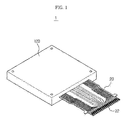
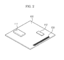
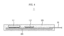
- a printed circuit board assembly 1 includes a printed circuit board 100, electronic components 111 and 112 mounted on the printed circuit board 100, and a flexible printed circuit board 20 connected to the printed circuit board 100.
- a conventional printed circuit board is formed by printing a blue lead resist on after forming a wiring with a copper foil on a thin board serving as a basis that is made of an insulator such as epoxy resin or Bakelite resin.
- the printed circuit board 100 is a wafer printed circuit board formed by performing a re-wiring on a wafer.
- a circuit is formed by a semiconductor re-wiring process, and thus, may embody a fine pattern capable of mounting a fine pitch component that could not be embodied on the conventional printed circuit board.
- Material of a wafer used for the wafer printed circuit board 100 may be silicon, glass, ceramic, or an organic.
- the organic matter may be a low coefficient thermal expansion (CTE) organic.
- Each of the electronic components 111 and 112 may be a component which comes in a package shape that is generally used, or a semiconductor chip at a wafer level. However, since an embodiment relates to the miniaturizing and the slimming of the printed circuit board assembly 1, each of the electronic component 111 and the electronic component 112 is desired to be the semiconductor chip at the wafer level. In a case that each of the electronic component 111 and the electronic component 112 is the semiconductor chip at the wafer level, the electronic components 111 and 112 may be directly mounted on the wafer printed circuit board 100 by using a solder ball. Since the wafer printed circuit board 100 is formed with the wafer itself, mounting the semiconductor chip is easy. In regard to a difficulty with a wiring, since the circuit may be formed by performing a semiconductor re-wiring on the wafer printed circuit board 100, the wiring of the circuit having a fine pattern may be embodied.
- An electrode for connection 130 configured for electrically connecting the wafer printed circuit board 100 to an outside sub board (not shown) is provided at one end edge of the wafer printed circuit board 100.
- a flexible PCB (FPCB) 20 is connected to the electrode for connection 130 while making contact with the electrode for connection 130.
- the flexible PCB 20 is referred to as a board using a flexible insulation board.
- the flexible PCB 20 may be formed by using a flexible material such as polyester (PET) or a heat resistance plastic film such as polyimide (PI).
- PET polyester
- PI polyimide
- An inner electrode 21 configured to be electrically and physically connected to the wafer printed circuit board 100 is formed at one end of the flexible PCB 20, and an outer electrode 22 configured to be electrically and physically connected to an outside sub board (not shown) is formed at the other end of the flexible PCB 20.
- the wafer printed circuit board 100 is directly attached to the flexible PCB 20 without the connector.
- the flexible PCB 20 is attached to the wafer printed circuit board 100 by using an adhesive agent. As the inner electrode 21 of the flexible PCB 20 is attached to the electrode for connection 130 of the wafer printed circuit board 100 while making contact with each other, the flexible PCB 20 and the wafer printed circuit board 100 are electrically and physically connected to each other.
- the adhesive agent a solder paste or an Anisotropic Conductive Film (ACF) is used.
- ACF Anisotropic Conductive Film
- any other adhesive agent which is configured to electrically and physically connect the flexible PCB 20 to the wafer printed circuit board 100 are included in an aspect of an embodiment.
- the miniaturizing and the slimming of the printed circuit board assembly 1 may be achieved.
- the wafer printed circuit board 100 having the electronic components 111 and 112 mounted thereon and having the flexible PCB 20 connected thereto is weak against an outside impact, the wafer printed circuit board 100 is covered with a protection body 120 that is formed by entirely molding the wafer printed circuit board 100 with a resin. Even if the protection body 120 covers the printed circuit board assembly 1, the outer electrode 22 of the flexible PCB 20 is needed to be connected to the outside sub board (not shown), thereby is exposed to the outside of the protection body 120.
- the protection body 120 ensures enough of mechanical strength of the printed circuit board assembly 1, and at the same time, may be able to protect the electronic components 111 and 112.
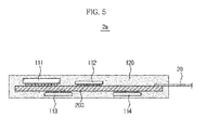
- FIG. 5 is a cross-sectional view of a printed circuit board assembly 2a according to an embodiment.
- the printed circuit board assembly 2a comprises wafer printed circuit board 200.
- a circuit wiring is formed on both sides of a wafer printed circuit board 200, and electronic components 111, 112, 113, and 114 are mounted on the both sides of the wafer printed circuit board 200.
- Each of the electronic components 111, 112, 113, and 114 is a semiconductor chip at a wafer level, and is directly mounted on the wafer printed circuit board 200 by using a solder ball.
- the electrode for connection 130 (refer to FIG. 2 ) configured for the electrical connection to the outside sub board (not shown) is provided at the one side edge of the wafer printed circuit board 200, and the flexible PCB 20 is connected to the electrode for connection 130 while making contact with the electrode for connection 130.
- One end of the flexible PCB 20 is electrically and physically connected to the wafer printed circuit board 200, and the other end of the flexible PCB 20 is electrically and physically connected to the outside sub board (not shown).
- the flexible PCB 20 is attached to the wafer printed circuit board 200 by using the adhesive agent, and no separate connector is needed.
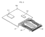
- FIG. 6A is a view illustrating an inner structure of a printed circuit board assembly prior to a molding according to an embodiment.
- FIG. 6B is a cross-sectional view of the printed circuit board assembly according to FIG. 6A .
- a first wafer printed circuit board 201 is electrically and physically connected to a second wafer printed circuit board 202 through a connection flexible printed circuit board 30.
- an electrode configured for being connected to the electrodes 30,31 of the connection flexible printed circuit board 30 is provided at each of the first wafer printed circuit board 201 and the second wafer printed circuit board 202.
- connection flexible printed circuit board 30 is attached to the first wafer printed circuit board 201 and the second wafer printed circuit board 202 by using the adhesive agent, and no separate connector is needed.
- the electronic components 111, 112, 113, and 114 formed with a semiconductor chip at a wafer level are mounted at each of one side of the first wafer printed circuit board 201 and the second wafer printed circuit board 202.
- the electronic components 111, 112, 113, and 114 are directly mounted on the wafer printed circuit board 200 as a wafer level by using the solder ball.
- the electrode for connection 120 (refer to FIG. 3 ) configured for the electrical connection to the outside sub board (not shown) is provided at the one side edge of the first wafer printed circuit board 201, and the flexible PCB 20 is connected to the electrode for connection 120 while making contact with the electrode for connection 120.
- One end of the flexible PCB 20 is electrically and physically connected to the wafer printed circuit board 200, and the other end of the flexible PCB 20 is electrically and physically connected to the outside sub board (not shown).
- the flexible PCB 20 is attached to the wafer printed circuit board 200 by using the adhesive agent, and no separate connector is needed, as previously explained.
- connection flexible printed circuit board 30 As illustrated on FIG. 6B , by folding the connection flexible printed circuit board 30 such that rear surfaces of the first wafer printed circuit board 201 and the second wafer printed circuit board 202 face each other, the rear surfaces not having the electronic components 111, 112, 113, and 114 mounted thereon, the same effect is attained as the electronic components 111, 112, 113, and 114 are mounted at both sides.
- each of the first wafer printed circuit board 201 and the second wafer printed circuit board 202 is not thick, the thickness of the first wafer printed circuit board 201 and the second wafer printed circuit board 202 stacked on top of one another does not become thicker.
- the double-sided printed circuit board In order to manufacture the double-sided printed circuit board according to an embodiment shown on FIG. 5 , a separate process is needed. However, according to an embodiment shown in FIG. 6A , the same degree of integration as the double sided printed circuit board is achieved by using a general one sided wafer printed circuit board.
- the printed circuit board assembly is composed as above, since there is no need to conduct a wiring process twice on each side of a single wafer printed circuit board, a cost reduction effect may be achieved.
- the protection body 120 is formed by entirely molding the first wafer printed circuit board 201 and the second wafer printed circuit board 202 stacked on top of one another by using the resin.
- the protection body 120 ensures enough of mechanical strength of the printed circuit board assembly 2b, thereby having stability, and at the same time, may be able to protect the electronic components 111, 112, 113, and 114.
- the flexible printed circuit board 20 is needed to be connected to the outside sub board (not shown), thereby is exposed to the outside of the protection body 120.
- FIG. 7 is a view showing a connection relation of a printed circuit board assembly according to an embodiment and a sub board.
- a printed circuit board assembly 3a includes the wafer printed circuit board 200, electronic components, and 112, mounted at the wafer printed circuit board 200, the flexible PCB 20 and a flexible PCB 40.
- the printed circuit board 200 according to an embodiment represents a wafer printed circuit board at which a circuit wiring is formed by conducting are-wiring on the wafer.
- Each of the electronic components 111 and 112 may be a component which comes in a package shape that is generally used, or a semiconductor chip at a wafer level. Particularly, in a case that the electronic component is provided as a wafer level such as a semiconductor chip, the electronic component is directly mounted at the wafer printed circuit board 200 without a separate interposer or the wiring.
- a first electrode for connection (not shown) is provided at one side edge of the wafer printed circuit board 200 for the electrical and physical connection to an outside sub board 300.
- the first flexible PCB 20 is connected to the first electrode for connection (not shown) while making contact with the first electrode.
- a second electrode for connection (not shown) is provided at the other side edge of the wafer printed circuit board 200 for the electrical and physical connection with another board (not shown).
- the second flexible PCB 40 is connected to the second electrode for connection (not shown) while making contact with the second electrode.
- the first flexible PCB 20 and the second first flexible PCB 40 include an inner electrode 21 and an inner electrode 41, respectively, for the connection with the wafer printed circuit board 200, and an outer electrode 22 and an outer electrode 42, respectively, for the connection with the outside board.
- the first flexible PCB 20 and the second flexible PCB 40 are attached to the wafer printed circuit board 200 by using the adhesive agent.
- the adhesive agent the solder paste or the Anisotropic Conductive Film (ACF) is used.
- the miniaturizing and the slimming of the printed circuit board assembly 3a may be achieved.
- the wafer printed circuit board 200 having the electronic components 111 and 112 mounted thereon and the first flexible PCB 20 and the second flexible PCB 40 connected thereto is entirely molded with a resin, thereby forming the protection body 120 that is configured to form an exterior of the printed circuit board assembly 3aand absorb impact.
- the protection body 120 covers the printed circuit board assembly 3a, the outer electrodes 22 and 42 of each of the first flexible PCB 20 and the second flexible PCB 40 are exposed to the outside of the protection body 120.
- the outside sub board 300 is connected to the outer electrode 22 of the first flexible PCB 20 which is exposed to the outside of the protection body 120.
- the outside sub board 300 is a wafer printed circuit board formed with a wafer.
- the outer electrode 22 of the first flexible printed circuit board 20 is directly connected to the outside sub board 300 without a structure such as a connector.
- Electronic components 311 and 312 may be directly mounted at the outside sub board 300 in the form of a semiconductor chip at a wafer level.
- FIG. 8 is a view showing a connection relation of a printed circuit board assembly an embodiment and a sub board.
- the protection body 120 configured to entirely cover a wafer printed circuit board (not shown) having an electronic component mounted thereon forms the exterior of the printed circuit board assembly 3b.
- One end of each of the first flexible PCB 20 which is configured for connection to an outside sub board 400 and the second flexible PCB is exposed to the outside of the protection body 120.
- the outer electrode 22 is formed at the one end of the first flexible PCB 20 for the connection to the outside sub board 400.
- the outside sub board 400 is a printed circuit board formed by using epoxy resin or Bakelite resin as a basis.
- the outer electrode 22 of the first flexible printed circuit board 20 may not be directly connected to the outside sub board 400 while making a contact with the outside sub board 400.
- a connector 414 configured for the electrical and physical connection to the first flexible printed circuit board 20 is mounted at the outside sub board 400. As the outer electrode 22 of the first flexible printed circuit board 20 is inserted into the connector 414, the first flexible printed circuit board 20 and the outside sub board 400 are connected to each other. Accordingly, the printed circuit board assembly 3b is electrically connected to the outside sub board 400.
- outside sub board 400 is a general printed circuit board
- electronic components 411, 412, and 413 may not be mounted as a wafer level, but are mounted in the form of a general package shape on the outside sub board 400.
- a plurality of lead wires 420 configured for the electrical connection with the outside sub board 400 is protruded from the electronic components 411, 412, and 413, to an outside.
- the lead wire 420 is soldered to the sub board 400, the electronic components 411, 412, and 413 are physically fixed to the sub board 400, and at the same time, are electrically connected to the sub board 400.
- the electronic apparatus may be reduced in size. Therefore, only by composing the main board with the printed circuit board assembly 3b according to an embodiment and by composing sub boards with the conventional printed circuit board, the miniaturizing and the slimming of the electronic apparatus may be achieved.
Landscapes
- Engineering & Computer Science (AREA)
- Microelectronics & Electronic Packaging (AREA)
- Manufacturing & Machinery (AREA)
- Combinations Of Printed Boards (AREA)
Applications Claiming Priority (1)
| Application Number | Priority Date | Filing Date | Title |
|---|---|---|---|
| KR1020110098254A KR101772490B1 (ko) | 2011-09-28 | 2011-09-28 | 인쇄회로기판 어셈블리 |
Publications (3)
| Publication Number | Publication Date |
|---|---|
| EP2575417A2 true EP2575417A2 (de) | 2013-04-03 |
| EP2575417A3 EP2575417A3 (de) | 2014-09-10 |
| EP2575417B1 EP2575417B1 (de) | 2018-10-31 |
Family
ID=46940379
Family Applications (1)
| Application Number | Title | Priority Date | Filing Date |
|---|---|---|---|
| EP12185845.0A Not-in-force EP2575417B1 (de) | 2011-09-28 | 2012-09-25 | Leiterplattenanordnung |
Country Status (6)
| Country | Link |
|---|---|
| US (1) | US8971047B2 (de) |
| EP (1) | EP2575417B1 (de) |
| KR (1) | KR101772490B1 (de) |
| CN (1) | CN103037619B (de) |
| BR (1) | BR102012023737A8 (de) |
| RU (1) | RU2012141224A (de) |
Families Citing this family (6)
| Publication number | Priority date | Publication date | Assignee | Title |
|---|---|---|---|---|
| US9991616B2 (en) * | 2016-03-18 | 2018-06-05 | Apple Inc. | SMT connection of rigid and flexible printed circuit boards |
| CN107403784B (zh) * | 2016-05-19 | 2020-04-24 | 胡川 | 线路板制作方法及结构 |
| US10276487B1 (en) | 2017-10-18 | 2019-04-30 | Micron Technology, Inc. | Semiconductor device with flexible circuit for enabling non-destructive attaching and detaching of device to system board |
| KR102537318B1 (ko) * | 2018-10-19 | 2023-05-26 | 삼성전자 주식회사 | 회로 기판 어셈블리 및 그것을 포함하는 전자 장치 |
| CN109561649B (zh) * | 2018-12-20 | 2024-04-26 | 苏州光韵达自动化设备有限公司 | 一种自动拼板机 |
| KR102444299B1 (ko) | 2020-10-23 | 2022-09-15 | 삼성전기주식회사 | 전자 소자 모듈 및 이의 제조 방법 |
Family Cites Families (21)
| Publication number | Priority date | Publication date | Assignee | Title |
|---|---|---|---|---|
| US3934074A (en) | 1974-04-22 | 1976-01-20 | Trw Inc. | Ceramic circuit board mounted in housing and method of fabrication thereof |
| US5108819A (en) | 1990-02-14 | 1992-04-28 | Eli Lilly And Company | Thin film electrical component |
| US5247423A (en) | 1992-05-26 | 1993-09-21 | Motorola, Inc. | Stacking three dimensional leadless multi-chip module and method for making the same |
| RU2190284C2 (ru) | 1998-07-07 | 2002-09-27 | Закрытое акционерное общество "Техно-ТМ" | Двусторонний электронный прибор |
| JP3673422B2 (ja) | 1999-03-12 | 2005-07-20 | 株式会社オートネットワーク技術研究所 | 分岐接続箱 |
| JP4022040B2 (ja) * | 2000-10-05 | 2007-12-12 | 松下電器産業株式会社 | 半導体デバイス |
| US6501525B2 (en) * | 2000-12-08 | 2002-12-31 | Industrial Technology Research Institute | Method for interconnecting a flat panel display having a non-transparent substrate and devices formed |
| KR100410946B1 (ko) * | 2001-05-16 | 2003-12-18 | 삼성전기주식회사 | 이미지 센서 모듈 및 그 제조 방법 |
| JP2003080694A (ja) | 2001-06-26 | 2003-03-19 | Seiko Epson Corp | 膜パターンの形成方法、膜パターン形成装置、導電膜配線、電気光学装置、電子機器、並びに非接触型カード媒体 |
| KR100476558B1 (ko) * | 2002-05-27 | 2005-03-17 | 삼성전기주식회사 | 이미지 센서 모듈 및 그 제작 공정 |
| US20040178514A1 (en) | 2003-03-12 | 2004-09-16 | Lee Sang-Hyeop | Method of encapsulating semiconductor devices on a printed circuit board, and a printed circuit board for use in the method |
| DE10336634B3 (de) * | 2003-08-08 | 2005-02-03 | Siemens Ag | Elektronisches Gerät |
| JP2006294902A (ja) | 2005-04-12 | 2006-10-26 | Matsushita Electric Ind Co Ltd | 差動増幅回路及び無線通信装置 |
| RU2312474C2 (ru) | 2005-07-13 | 2007-12-10 | Геннадий Андреевич Блинов | Прецизионный гибкий шлейф и способ высокоплотного монтажа электронных приборов с помощью таких шлейфов |
| KR100718324B1 (ko) | 2005-10-20 | 2007-05-17 | (주) 에프원미디어 | 블루투스 모듈 인쇄회로기판 |
| KR20070103141A (ko) | 2006-04-18 | 2007-10-23 | 삼성전자주식회사 | 반사판 일체형 회로 기판 및 이를 이용한 액정표시장치 |
| TWI329915B (en) | 2006-06-02 | 2010-09-01 | Chiplus Semiconductor Corp | Method and structure for fabricating circuit board via wafer |
| US7739791B2 (en) * | 2007-10-26 | 2010-06-22 | Delphi Technologies, Inc. | Method of producing an overmolded electronic module with a flexible circuit pigtail |
| KR20090057720A (ko) * | 2007-12-03 | 2009-06-08 | 엘지전자 주식회사 | 플라즈마 디스플레이 장치 |
| KR20100011584A (ko) | 2008-07-25 | 2010-02-03 | 삼성전기주식회사 | 경연성 인쇄회로기판 |
| JP2010223690A (ja) * | 2009-03-23 | 2010-10-07 | Seiko Epson Corp | フレキシブル基板、並びに電気光学装置及び電子機器 |
-
2011
- 2011-09-28 KR KR1020110098254A patent/KR101772490B1/ko not_active Expired - Fee Related
-
2012
- 2012-09-11 US US13/610,145 patent/US8971047B2/en not_active Expired - Fee Related
- 2012-09-20 BR BR102012023737A patent/BR102012023737A8/pt not_active Application Discontinuation
- 2012-09-25 EP EP12185845.0A patent/EP2575417B1/de not_active Not-in-force
- 2012-09-26 RU RU2012141224/07A patent/RU2012141224A/ru unknown
- 2012-09-28 CN CN201210367702.4A patent/CN103037619B/zh not_active Expired - Fee Related
Non-Patent Citations (1)
| Title |
|---|
| None |
Also Published As
| Publication number | Publication date |
|---|---|
| US8971047B2 (en) | 2015-03-03 |
| BR102012023737A2 (pt) | 2013-11-12 |
| CN103037619B (zh) | 2018-08-03 |
| BR102012023737A8 (pt) | 2018-05-15 |
| KR101772490B1 (ko) | 2017-08-30 |
| EP2575417B1 (de) | 2018-10-31 |
| US20130077265A1 (en) | 2013-03-28 |
| KR20130034310A (ko) | 2013-04-05 |
| CN103037619A (zh) | 2013-04-10 |
| EP2575417A3 (de) | 2014-09-10 |
| RU2012141224A (ru) | 2014-04-10 |
Similar Documents
| Publication | Publication Date | Title |
|---|---|---|
| JP6822940B2 (ja) | 回路基板 | |
| US20130161078A1 (en) | Rigid-flex circuit board and manufacturing method | |
| EP2575417B1 (de) | Leiterplattenanordnung | |
| US20070170582A1 (en) | Component-containing module and method for producing the same | |
| JP6745770B2 (ja) | 回路基板 | |
| CN1778153A (zh) | 印刷布线板的连接结构 | |
| JP6783724B2 (ja) | 回路基板 | |
| US7762819B2 (en) | Substrate connecting member and connecting structure | |
| US9585260B2 (en) | Electronic component module and manufacturing method thereof | |
| US8197284B2 (en) | Printed circuit board assembly and connecting method thereof | |
| US20110007482A1 (en) | Printed circuit board unit and electronic device | |
| US9673123B2 (en) | Electronic device module and method of manufacturing the same | |
| KR101167453B1 (ko) | 전자부품 내장형 인쇄회로기판 및 그 제조방법 | |
| JP2019040903A (ja) | 回路基板及び半導体モジュール | |
| CN205755064U (zh) | 元件载体 | |
| JP2001008068A (ja) | 投影面積を小さくし立体化したセンサモジュール | |
| KR20120004088A (ko) | 인쇄회로기판 제조 방법 | |
| WO2017077837A1 (ja) | 部品実装基板 | |
| US20140293560A1 (en) | Substrate embedding electronic component and method of manufacturing substrate embedding electronic component | |
| KR100661653B1 (ko) | 기판조립체 | |
| WO2017038791A1 (ja) | 樹脂回路基板、部品搭載樹脂回路基板 | |
| US20120162946A1 (en) | Electronic device | |
| KR20020005823A (ko) | 테이프 배선기판을 이용한 볼 그리드 어레이 패키지 | |
| KR20090093673A (ko) | 인쇄회로기판의 제조방법 | |
| JP2001007512A (ja) | 超小型化した複数枚の回路基板相互間の電気的接続方法 |
Legal Events
| Date | Code | Title | Description |
|---|---|---|---|
| PUAI | Public reference made under article 153(3) epc to a published international application that has entered the european phase |
Free format text: ORIGINAL CODE: 0009012 |
|
| AK | Designated contracting states |
Kind code of ref document: A2 Designated state(s): AL AT BE BG CH CY CZ DE DK EE ES FI FR GB GR HR HU IE IS IT LI LT LU LV MC MK MT NL NO PL PT RO RS SE SI SK SM TR |
|
| AX | Request for extension of the european patent |
Extension state: BA ME |
|
| PUAL | Search report despatched |
Free format text: ORIGINAL CODE: 0009013 |
|
| RIC1 | Information provided on ipc code assigned before grant |
Ipc: H05K 1/14 20060101ALI20140731BHEP Ipc: H05K 1/18 20060101AFI20140731BHEP |
|
| AK | Designated contracting states |
Kind code of ref document: A3 Designated state(s): AL AT BE BG CH CY CZ DE DK EE ES FI FR GB GR HR HU IE IS IT LI LT LU LV MC MK MT NL NO PL PT RO RS SE SI SK SM TR |
|
| AX | Request for extension of the european patent |
Extension state: BA ME |
|
| 17P | Request for examination filed |
Effective date: 20150310 |
|
| RBV | Designated contracting states (corrected) |
Designated state(s): AL AT BE BG CH CY CZ DE DK EE ES FI FR GB GR HR HU IE IS IT LI LT LU LV MC MK MT NL NO PL PT RO RS SE SI SK SM TR |
|
| REG | Reference to a national code |
Ref country code: DE Ref legal event code: R079 Ref document number: 602012052816 Country of ref document: DE Free format text: PREVIOUS MAIN CLASS: H05K0001180000 Ipc: H05K0001140000 |
|
| RIC1 | Information provided on ipc code assigned before grant |
Ipc: H05K 3/28 20060101ALN20180126BHEP Ipc: H05K 5/06 20060101ALN20180126BHEP Ipc: H05K 1/18 20060101ALI20180126BHEP Ipc: H05K 1/14 20060101AFI20180126BHEP Ipc: H05K 3/32 20060101ALN20180126BHEP Ipc: H05K 3/36 20060101ALN20180126BHEP |
|
| GRAP | Despatch of communication of intention to grant a patent |
Free format text: ORIGINAL CODE: EPIDOSNIGR1 |
|
| STAA | Information on the status of an ep patent application or granted ep patent |
Free format text: STATUS: GRANT OF PATENT IS INTENDED |
|
| INTG | Intention to grant announced |
Effective date: 20180405 |
|
| GRAS | Grant fee paid |
Free format text: ORIGINAL CODE: EPIDOSNIGR3 |
|
| RAP1 | Party data changed (applicant data changed or rights of an application transferred) |
Owner name: SAMSUNG ELECTRONICS CO., LTD. |
|
| GRAA | (expected) grant |
Free format text: ORIGINAL CODE: 0009210 |
|
| STAA | Information on the status of an ep patent application or granted ep patent |
Free format text: STATUS: THE PATENT HAS BEEN GRANTED |
|
| AK | Designated contracting states |
Kind code of ref document: B1 Designated state(s): AL AT BE BG CH CY CZ DE DK EE ES FI FR GB GR HR HU IE IS IT LI LT LU LV MC MK MT NL NO PL PT RO RS SE SI SK SM TR |
|
| REG | Reference to a national code |
Ref country code: CH Ref legal event code: EP Ref country code: GB Ref legal event code: FG4D |
|
| REG | Reference to a national code |
Ref country code: AT Ref legal event code: REF Ref document number: 1060965 Country of ref document: AT Kind code of ref document: T Effective date: 20181115 |
|
| REG | Reference to a national code |
Ref country code: DE Ref legal event code: R096 Ref document number: 602012052816 Country of ref document: DE |
|
| REG | Reference to a national code |
Ref country code: IE Ref legal event code: FG4D |
|
| REG | Reference to a national code |
Ref country code: NL Ref legal event code: FP |
|
| REG | Reference to a national code |
Ref country code: LT Ref legal event code: MG4D |
|
| REG | Reference to a national code |
Ref country code: AT Ref legal event code: MK05 Ref document number: 1060965 Country of ref document: AT Kind code of ref document: T Effective date: 20181031 |
|
| PG25 | Lapsed in a contracting state [announced via postgrant information from national office to epo] |
Ref country code: PL Free format text: LAPSE BECAUSE OF FAILURE TO SUBMIT A TRANSLATION OF THE DESCRIPTION OR TO PAY THE FEE WITHIN THE PRESCRIBED TIME-LIMIT Effective date: 20181031 Ref country code: HR Free format text: LAPSE BECAUSE OF FAILURE TO SUBMIT A TRANSLATION OF THE DESCRIPTION OR TO PAY THE FEE WITHIN THE PRESCRIBED TIME-LIMIT Effective date: 20181031 Ref country code: LT Free format text: LAPSE BECAUSE OF FAILURE TO SUBMIT A TRANSLATION OF THE DESCRIPTION OR TO PAY THE FEE WITHIN THE PRESCRIBED TIME-LIMIT Effective date: 20181031 Ref country code: AT Free format text: LAPSE BECAUSE OF FAILURE TO SUBMIT A TRANSLATION OF THE DESCRIPTION OR TO PAY THE FEE WITHIN THE PRESCRIBED TIME-LIMIT Effective date: 20181031 Ref country code: BG Free format text: LAPSE BECAUSE OF FAILURE TO SUBMIT A TRANSLATION OF THE DESCRIPTION OR TO PAY THE FEE WITHIN THE PRESCRIBED TIME-LIMIT Effective date: 20190131 Ref country code: IS Free format text: LAPSE BECAUSE OF FAILURE TO SUBMIT A TRANSLATION OF THE DESCRIPTION OR TO PAY THE FEE WITHIN THE PRESCRIBED TIME-LIMIT Effective date: 20190228 Ref country code: ES Free format text: LAPSE BECAUSE OF FAILURE TO SUBMIT A TRANSLATION OF THE DESCRIPTION OR TO PAY THE FEE WITHIN THE PRESCRIBED TIME-LIMIT Effective date: 20181031 Ref country code: NO Free format text: LAPSE BECAUSE OF FAILURE TO SUBMIT A TRANSLATION OF THE DESCRIPTION OR TO PAY THE FEE WITHIN THE PRESCRIBED TIME-LIMIT Effective date: 20190131 Ref country code: FI Free format text: LAPSE BECAUSE OF FAILURE TO SUBMIT A TRANSLATION OF THE DESCRIPTION OR TO PAY THE FEE WITHIN THE PRESCRIBED TIME-LIMIT Effective date: 20181031 Ref country code: LV Free format text: LAPSE BECAUSE OF FAILURE TO SUBMIT A TRANSLATION OF THE DESCRIPTION OR TO PAY THE FEE WITHIN THE PRESCRIBED TIME-LIMIT Effective date: 20181031 |
|
| PG25 | Lapsed in a contracting state [announced via postgrant information from national office to epo] |
Ref country code: RS Free format text: LAPSE BECAUSE OF FAILURE TO SUBMIT A TRANSLATION OF THE DESCRIPTION OR TO PAY THE FEE WITHIN THE PRESCRIBED TIME-LIMIT Effective date: 20181031 Ref country code: SE Free format text: LAPSE BECAUSE OF FAILURE TO SUBMIT A TRANSLATION OF THE DESCRIPTION OR TO PAY THE FEE WITHIN THE PRESCRIBED TIME-LIMIT Effective date: 20181031 Ref country code: AL Free format text: LAPSE BECAUSE OF FAILURE TO SUBMIT A TRANSLATION OF THE DESCRIPTION OR TO PAY THE FEE WITHIN THE PRESCRIBED TIME-LIMIT Effective date: 20181031 Ref country code: GR Free format text: LAPSE BECAUSE OF FAILURE TO SUBMIT A TRANSLATION OF THE DESCRIPTION OR TO PAY THE FEE WITHIN THE PRESCRIBED TIME-LIMIT Effective date: 20190201 Ref country code: PT Free format text: LAPSE BECAUSE OF FAILURE TO SUBMIT A TRANSLATION OF THE DESCRIPTION OR TO PAY THE FEE WITHIN THE PRESCRIBED TIME-LIMIT Effective date: 20190301 |
|
| PG25 | Lapsed in a contracting state [announced via postgrant information from national office to epo] |
Ref country code: DK Free format text: LAPSE BECAUSE OF FAILURE TO SUBMIT A TRANSLATION OF THE DESCRIPTION OR TO PAY THE FEE WITHIN THE PRESCRIBED TIME-LIMIT Effective date: 20181031 Ref country code: IT Free format text: LAPSE BECAUSE OF FAILURE TO SUBMIT A TRANSLATION OF THE DESCRIPTION OR TO PAY THE FEE WITHIN THE PRESCRIBED TIME-LIMIT Effective date: 20181031 Ref country code: CZ Free format text: LAPSE BECAUSE OF FAILURE TO SUBMIT A TRANSLATION OF THE DESCRIPTION OR TO PAY THE FEE WITHIN THE PRESCRIBED TIME-LIMIT Effective date: 20181031 |
|
| REG | Reference to a national code |
Ref country code: DE Ref legal event code: R097 Ref document number: 602012052816 Country of ref document: DE |
|
| PG25 | Lapsed in a contracting state [announced via postgrant information from national office to epo] |
Ref country code: RO Free format text: LAPSE BECAUSE OF FAILURE TO SUBMIT A TRANSLATION OF THE DESCRIPTION OR TO PAY THE FEE WITHIN THE PRESCRIBED TIME-LIMIT Effective date: 20181031 Ref country code: EE Free format text: LAPSE BECAUSE OF FAILURE TO SUBMIT A TRANSLATION OF THE DESCRIPTION OR TO PAY THE FEE WITHIN THE PRESCRIBED TIME-LIMIT Effective date: 20181031 Ref country code: SM Free format text: LAPSE BECAUSE OF FAILURE TO SUBMIT A TRANSLATION OF THE DESCRIPTION OR TO PAY THE FEE WITHIN THE PRESCRIBED TIME-LIMIT Effective date: 20181031 Ref country code: SK Free format text: LAPSE BECAUSE OF FAILURE TO SUBMIT A TRANSLATION OF THE DESCRIPTION OR TO PAY THE FEE WITHIN THE PRESCRIBED TIME-LIMIT Effective date: 20181031 |
|
| PLBE | No opposition filed within time limit |
Free format text: ORIGINAL CODE: 0009261 |
|
| STAA | Information on the status of an ep patent application or granted ep patent |
Free format text: STATUS: NO OPPOSITION FILED WITHIN TIME LIMIT |
|
| 26N | No opposition filed |
Effective date: 20190801 |
|
| PG25 | Lapsed in a contracting state [announced via postgrant information from national office to epo] |
Ref country code: SI Free format text: LAPSE BECAUSE OF FAILURE TO SUBMIT A TRANSLATION OF THE DESCRIPTION OR TO PAY THE FEE WITHIN THE PRESCRIBED TIME-LIMIT Effective date: 20181031 |
|
| PG25 | Lapsed in a contracting state [announced via postgrant information from national office to epo] |
Ref country code: TR Free format text: LAPSE BECAUSE OF FAILURE TO SUBMIT A TRANSLATION OF THE DESCRIPTION OR TO PAY THE FEE WITHIN THE PRESCRIBED TIME-LIMIT Effective date: 20181031 |
|
| PG25 | Lapsed in a contracting state [announced via postgrant information from national office to epo] |
Ref country code: MC Free format text: LAPSE BECAUSE OF FAILURE TO SUBMIT A TRANSLATION OF THE DESCRIPTION OR TO PAY THE FEE WITHIN THE PRESCRIBED TIME-LIMIT Effective date: 20181031 |
|
| REG | Reference to a national code |
Ref country code: CH Ref legal event code: PL |
|
| PG25 | Lapsed in a contracting state [announced via postgrant information from national office to epo] |
Ref country code: LI Free format text: LAPSE BECAUSE OF NON-PAYMENT OF DUE FEES Effective date: 20190930 Ref country code: LU Free format text: LAPSE BECAUSE OF NON-PAYMENT OF DUE FEES Effective date: 20190925 Ref country code: CH Free format text: LAPSE BECAUSE OF NON-PAYMENT OF DUE FEES Effective date: 20190930 Ref country code: IE Free format text: LAPSE BECAUSE OF NON-PAYMENT OF DUE FEES Effective date: 20190925 |
|
| REG | Reference to a national code |
Ref country code: BE Ref legal event code: MM Effective date: 20190930 |
|
| PG25 | Lapsed in a contracting state [announced via postgrant information from national office to epo] |
Ref country code: BE Free format text: LAPSE BECAUSE OF NON-PAYMENT OF DUE FEES Effective date: 20190930 |
|
| PGFP | Annual fee paid to national office [announced via postgrant information from national office to epo] |
Ref country code: NL Payment date: 20200821 Year of fee payment: 9 |
|
| PG25 | Lapsed in a contracting state [announced via postgrant information from national office to epo] |
Ref country code: FR Free format text: LAPSE BECAUSE OF NON-PAYMENT OF DUE FEES Effective date: 20190930 |
|
| PGFP | Annual fee paid to national office [announced via postgrant information from national office to epo] |
Ref country code: DE Payment date: 20200820 Year of fee payment: 9 Ref country code: GB Payment date: 20200824 Year of fee payment: 9 |
|
| PG25 | Lapsed in a contracting state [announced via postgrant information from national office to epo] |
Ref country code: CY Free format text: LAPSE BECAUSE OF FAILURE TO SUBMIT A TRANSLATION OF THE DESCRIPTION OR TO PAY THE FEE WITHIN THE PRESCRIBED TIME-LIMIT Effective date: 20181031 |
|
| PG25 | Lapsed in a contracting state [announced via postgrant information from national office to epo] |
Ref country code: MT Free format text: LAPSE BECAUSE OF FAILURE TO SUBMIT A TRANSLATION OF THE DESCRIPTION OR TO PAY THE FEE WITHIN THE PRESCRIBED TIME-LIMIT Effective date: 20181031 Ref country code: HU Free format text: LAPSE BECAUSE OF FAILURE TO SUBMIT A TRANSLATION OF THE DESCRIPTION OR TO PAY THE FEE WITHIN THE PRESCRIBED TIME-LIMIT; INVALID AB INITIO Effective date: 20120925 |
|
| REG | Reference to a national code |
Ref country code: DE Ref legal event code: R119 Ref document number: 602012052816 Country of ref document: DE |
|
| REG | Reference to a national code |
Ref country code: NL Ref legal event code: MM Effective date: 20211001 |
|
| GBPC | Gb: european patent ceased through non-payment of renewal fee |
Effective date: 20210925 |
|
| PG25 | Lapsed in a contracting state [announced via postgrant information from national office to epo] |
Ref country code: NL Free format text: LAPSE BECAUSE OF NON-PAYMENT OF DUE FEES Effective date: 20211001 Ref country code: MK Free format text: LAPSE BECAUSE OF FAILURE TO SUBMIT A TRANSLATION OF THE DESCRIPTION OR TO PAY THE FEE WITHIN THE PRESCRIBED TIME-LIMIT Effective date: 20181031 |
|
| PG25 | Lapsed in a contracting state [announced via postgrant information from national office to epo] |
Ref country code: GB Free format text: LAPSE BECAUSE OF NON-PAYMENT OF DUE FEES Effective date: 20210925 Ref country code: DE Free format text: LAPSE BECAUSE OF NON-PAYMENT OF DUE FEES Effective date: 20220401 |