EP2575176B1 - Zusammengeklappte Haftbandverpackung für elektronische Vorrichtungen - Google Patents
Zusammengeklappte Haftbandverpackung für elektronische Vorrichtungen Download PDFInfo
- Publication number
- EP2575176B1 EP2575176B1 EP12186417.7A EP12186417A EP2575176B1 EP 2575176 B1 EP2575176 B1 EP 2575176B1 EP 12186417 A EP12186417 A EP 12186417A EP 2575176 B1 EP2575176 B1 EP 2575176B1
- Authority
- EP
- European Patent Office
- Prior art keywords
- flexible tape
- tape substrate
- middle section
- substrate
- die stack
- Prior art date
- Legal status (The legal status is an assumption and is not a legal conclusion. Google has not performed a legal analysis and makes no representation as to the accuracy of the status listed.)
- Active
Links
Images


Classifications
-
- H—ELECTRICITY
- H10—SEMICONDUCTOR DEVICES; ELECTRIC SOLID-STATE DEVICES NOT OTHERWISE PROVIDED FOR
- H10F—INORGANIC SEMICONDUCTOR DEVICES SENSITIVE TO INFRARED RADIATION, LIGHT, ELECTROMAGNETIC RADIATION OF SHORTER WAVELENGTH OR CORPUSCULAR RADIATION
- H10F39/00—Integrated devices, or assemblies of multiple devices, comprising at least one element covered by group H10F30/00, e.g. radiation detectors comprising photodiode arrays
- H10F39/80—Constructional details of image sensors
- H10F39/804—Containers or encapsulations
-
- H—ELECTRICITY
- H10—SEMICONDUCTOR DEVICES; ELECTRIC SOLID-STATE DEVICES NOT OTHERWISE PROVIDED FOR
- H10W—GENERIC PACKAGES, INTERCONNECTIONS, CONNECTORS OR OTHER CONSTRUCTIONAL DETAILS OF DEVICES COVERED BY CLASS H10
- H10W72/00—Interconnections or connectors in packages
- H10W72/01—Manufacture or treatment
- H10W72/0198—Manufacture or treatment batch processes
-
- H—ELECTRICITY
- H10—SEMICONDUCTOR DEVICES; ELECTRIC SOLID-STATE DEVICES NOT OTHERWISE PROVIDED FOR
- H10W—GENERIC PACKAGES, INTERCONNECTIONS, CONNECTORS OR OTHER CONSTRUCTIONAL DETAILS OF DEVICES COVERED BY CLASS H10
- H10W70/00—Package substrates; Interposers; Redistribution layers [RDL]
- H10W70/60—Insulating or insulated package substrates; Interposers; Redistribution layers
- H10W70/67—Insulating or insulated package substrates; Interposers; Redistribution layers characterised by their insulating layers or insulating parts
- H10W70/688—Flexible insulating substrates
-
- H—ELECTRICITY
- H10—SEMICONDUCTOR DEVICES; ELECTRIC SOLID-STATE DEVICES NOT OTHERWISE PROVIDED FOR
- H10W—GENERIC PACKAGES, INTERCONNECTIONS, CONNECTORS OR OTHER CONSTRUCTIONAL DETAILS OF DEVICES COVERED BY CLASS H10
- H10W72/00—Interconnections or connectors in packages
- H10W72/50—Bond wires
- H10W72/541—Dispositions of bond wires
- H10W72/5445—Dispositions of bond wires being orthogonal to a side surface of the chip, e.g. parallel arrangements
-
- H—ELECTRICITY
- H10—SEMICONDUCTOR DEVICES; ELECTRIC SOLID-STATE DEVICES NOT OTHERWISE PROVIDED FOR
- H10W—GENERIC PACKAGES, INTERCONNECTIONS, CONNECTORS OR OTHER CONSTRUCTIONAL DETAILS OF DEVICES COVERED BY CLASS H10
- H10W72/00—Interconnections or connectors in packages
- H10W72/50—Bond wires
- H10W72/551—Materials of bond wires
- H10W72/552—Materials of bond wires comprising metals or metalloids, e.g. silver
- H10W72/5522—Materials of bond wires comprising metals or metalloids, e.g. silver comprising gold [Au]
-
- H—ELECTRICITY
- H10—SEMICONDUCTOR DEVICES; ELECTRIC SOLID-STATE DEVICES NOT OTHERWISE PROVIDED FOR
- H10W—GENERIC PACKAGES, INTERCONNECTIONS, CONNECTORS OR OTHER CONSTRUCTIONAL DETAILS OF DEVICES COVERED BY CLASS H10
- H10W72/00—Interconnections or connectors in packages
- H10W72/90—Bond pads, in general
- H10W72/931—Shapes of bond pads
- H10W72/932—Plan-view shape, i.e. in top view
-
- Y—GENERAL TAGGING OF NEW TECHNOLOGICAL DEVELOPMENTS; GENERAL TAGGING OF CROSS-SECTIONAL TECHNOLOGIES SPANNING OVER SEVERAL SECTIONS OF THE IPC; TECHNICAL SUBJECTS COVERED BY FORMER USPC CROSS-REFERENCE ART COLLECTIONS [XRACs] AND DIGESTS
- Y10—TECHNICAL SUBJECTS COVERED BY FORMER USPC
- Y10T—TECHNICAL SUBJECTS COVERED BY FORMER US CLASSIFICATION
- Y10T29/00—Metal working
- Y10T29/49—Method of mechanical manufacture
- Y10T29/49002—Electrical device making
- Y10T29/49117—Conductor or circuit manufacturing
- Y10T29/49124—On flat or curved insulated base, e.g., printed circuit, etc.
Definitions
- This application is related to packaging of electronic imaging devices.
- US 2011/0102667 A1 discloses a method of manufacturing a camera module that includes providing an image capture device, providing an electronic component, providing a flexible circuit substrate, mounting the image capture device on a first portion of the flexible circuit substrate, mounting the electronic component on the second portion of the flexible circuit substrate, and positioning the second portion above the first portion.
- the method further includes providing a chip carrier including a bottom surface defining a cavity and a top surface adapted to receive the image capture device and positioning the chip carrier between the image capture device and the flexible circuit substrate.
- the method further includes mounting a second electronic component within the cavity.
- EP 2 437 296 A1 discloses a radiation detecting unit which is provided with a PD array including a plurality of PD elements arrayed opposite to a scintillator and output electrode pads arrayed corresponding to the PD elements integrated circuits for processing signals from the PD elements, a flexible substrate for mounting of the PD array and integrated circuits, and a radiation shield plate provided opposite to the PD array with the flexible substrate in between and formed so that ends thereof are located inside the PD array; the output electrode pads have an array pitch made shorter than that of PD elements; the flexible substrate is folded along the ends at intermediate regions between mounting regions of the PD array and integrated circuits, whereby the integrated circuits are arranged on the opposite side to the PD elements with the radiation shield plate in between.
- WO 2004/023546 A1 discloses a microelectronic package which is fabricated by a process which included folding a substrate. The substrate is folded by engaging a first end of the substrate with a die so that the first end pivots with respect to a central portion of the substrate. Next, a second end of the substrate is folded similar to the first end.
- US 2010/0134985 A1 discloses an image-sensing module for reducing its overall thickness and preventing electromagnetic interference (EMI) which includes a flexible substrate, an image sensor, and a plurality of electronic elements.
- the flexible substrate has a first PCB (Printed Circuit Board), a flexible bending board bent upwards from one side of the first PCB, and a second PCB extending forwards from the flexible bending board and disposed above the first PCB.
- the second PCB has at least one first opening.
- the image sensor is electrically disposed on the first PCB, and the image sensor is exposed by the first opening of the second PCB.
- the electronic elements are selectively electrically disposed on the first PCB and/or on the second PCB so that the electronic elements are disposed between the first PCB and the second PCB.
- US 2002/0167081 A1 discloses a flexible circuit substrate which has mounting regions on which electronic components are mainly mounted, respectively, and other electronic components are also mounted.
- the flexible circuit substrate is structured in such a manner that the mounting regions are folded on top of the other over the base region in a predetermined order.
- An integrated spacer has thick regions and thin regions, and is superposed and affixed to the flexible circuit substrate as indicated by arrows with broken lines, and supports the electronic components stacked in layers. Fixing bosses and aperture sections to be coupled therewith are provided to facilitate positioning.
- a camera module comprises:
- a camera module comprises:
- the camera module may further comprise: two or more LGA pads mounted on the bottom surface of the flexible tape substrate and two or more mounting pads mounted on the top surface of the flexible tape substrate.
- the camera module may further comprise: a stiffener attached to the imager die stack in the mold.
- the mold covered imager die stack may further comprise: a silicon substrate; an imager die attached to the silicon substrate; and at least one of a processor or memory attached to the silicon substrate and the imager die.
- the invention also includes a method for manufacturing a camera module according to the first or second aspect, comprising:
- the method may further comprise:
- the method may further comprise: covering the mounted passive components with a mold; and attaching a stiffener to the imager die stack.
- the folded tape package uses a flexible tape substrate having two end sections for passive components and a middle section for connecting and stacking multiple dies.
- the stacked dies are encapsulated or covered with a mold. One side may be left exposed for device functionality and operation with additional components or devices.
- the passive components may also be covered with a mold.
- the end sections are folded such that the end sections are in a parallel configuration with the middle section.
- the flexible tape substrate may be a high density interconnect (HDI) flexible tape substrate.
- the HDI flexible tape substrate may have two layers.
- a silicon substrate may be used to interconnect a die stack to the flexible tape substrate.
- the folded tape package has a reduced device footprint, lower substrate warpage effects, and higher substrate yields.
- Figures 16 - 29 show a flexible tape substrate, a process view and a flowchart for manufacturing a folded tape package not forming part of the present invention but useful for understanding thereof.
- the folded tape package uses a flexible tape substrate having two end sections for passive components and a middle section for connecting and stacking multiple dies.
- the stacked dies are encapsulated or covered with a mold. One side is left exposed for device functionality and operation with additional components or devices.
- the passive components may also be covered with a mold.
- the end sections are folded toward the mold covered stacked die side such that the end sections are in a parallel configuration with the middle section.
- the flexible tape substrate may be a high density interconnect ((HDI) flexible tape substrate with two layers.
- the flexible tape substrate may be made of polyimide and other like materials.
- the folded tape package has a reduced device footprint, lower substrate warpage effects, and higher substrate yields. As described herein, the folded tape package eliminates the need of the through silicon vias (TSVs) for signal routing.
- TSVs through silicon vias
- Figures 1-14 show an embodiment and process flow for a folded tape package.
- Figure 1 shows an embodiment of a flexible tape substrate strip 100 that may have multiple flexible tape substrate units 105.
- Each flexible tape substrate unit 105 may have a top surface 110 and a bottom surface 115.
- Each flexible tape substrate unit 105 may further have a first end section 120, a first fold section, 125, a middle section 130, a second fold section 135 and a second end section 140.
- the first end section 120 and the second end section 140 on the top surface 110 may have multiple surface mount (SMT) pads 145 for passive components, by way of non-limiting example.
- the middle section 130 on the top surface 110 may have a window cavity 150 for an imager chip or device, by way of non-limiting example.
- the window cavity 150 may have associated wire bonding pads 155 and flip chip pads 160.
- the first end section 120 and the second end section 140 on the bottom surface 110 may have a land grid array (LGA) 165, by way of non-limiting example.
- the flexible tape substrate and flexible tape substrate strip 100 may be manufactured, implemented or constructed using techniques and processes known to those of skill in the art.
- the flexible tape substrate may be a high density interconnect (HDI) flexible tape substrate and the like.
- the flexible tape substrate may be a two (2) layer flexible tape substrate as opposed to an eight (8) layer flexible tape substrate due to the folding configuration which increases
- warpage and thickness may controlled to within +/- 15 pm as opposed to a 8 layer flexible tape substrate which may have a +/- 60 ⁇ m variance.
- reducing the thickness of the flexible tape substrate reduces the overall height of the electronic device, for example, a camera module.
- the thin flexible tape substrate also permits the use of a single stud bump as opposed to a double stud bump, which may be needed for ceramic substrates. Ceramic substrates suffer from warpage and evenness issues and invariably need double stud bumps.
- the use of a single stud bump reduces costs as stud bumps are nominally made from gold wire.
- stud bumping may not be needed due to the flatness of the substrates being used.
- plated bumps may be used, which may reduce costs.
- the flexible tape substrate may also permit the use of a gang press as substrate warpage is not an issue and may increase the units per hour. Moreover, die mounting for dummy tape units may not be needed to even out bonding force issues as the flexible tape substrate has minimal warpage issues and the level of bonding force may be reduced. In addition, the die may not have to be stud bumped, which in turn may reduce further costs.
- the use of the gang press may allow multiple tape substrate units to be bonded at the same time. Nominally, the bonding process may take 15 seconds per unit. In a gang press implementation for the flexible tape substrate, each unit may undergo a one (1) second pre-bond. This may be followed by a gang press bonding of 30 units, by way of non-limiting example, which may be for 16-17 seconds, by way of non-limiting example.
- FIG. 2 shows a flexible tape substrate strip 200, where each flexible tape substrate unit 205 may have surface mounted passive components 210.
- the placement of the surface mounted passive components 210 may be accomplished using techniques and processes known to those of skill in the art.
- the placement of the surface mounted passive components may be done at the strip level to increase efficiencies and decrease costs. For example, by way of non-limiting example only, the units per hour may improved 30% or more by processing strips as opposed to ceramic coupon size.
- Figure 3 shows a flexible tape substrate unit 300 including a die 305.
- the die 305 may be an imager chip or some other electronic component.
- the die 305 is attached to the flexible tape substrate unit 300 using flip-chip bonding techniques and processes known to those of skill in the art. These may include, by way of non-limiting example only, thermo-compression or thermo-sonic flip chip bonding techniques.
- the bonding force may reduce because bonding on the flexible tape surface may require less force than a ceramic substrate with single bump geometry.
- a thinner die may be used due to a better coefficient of thermal expansion match between the flexible tape substrate and the silicon die and reduced bonding force.
- the die attachment may be done at the strip level to increase efficiencies and decrease costs.
- Figure 4 shows a flexible tape substrate unit 400 having a second die 405 attached to the die 305 of Figure 3 to form a die stack 410.
- the second die 405 may be a memory or processor die, by way of non-limiting example.
- the second die 405 may be implemented and attached to the flexible tape substrate unit 400 and die 305 using flip-chip bonding and wire bonding techniques and processes known to those of skill in the art.
- the die attachment may be done at the strip level to increase efficiencies and decrease costs.
- Figure 5 shows a flexible tape substrate unit 500 having an attached die stack (not visible) that is covered with a mold 505.
- the mold 505 may be implemented using mold transfer techniques and processes known to those of skill in the art. The mold transfer may be done at the strip level to increase efficiencies and decrease costs. In addition to covering the die stack, a mold transfer process may be used to cover the SMTs which may provide much better reliability and handling. The temperature may be raised on the molded side for better temperature balance during bonding. Bonding time may then be reduced, which may increase or improve the units per hour (i.e., production).
- Figure 6 shows a flexible tape substrate unit 600 that has a stiffener 610 attached to the mold covered die stack 605.
- the stiffener 610 attachment may be done at the strip level to increase efficiencies and decrease costs.
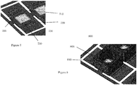
- Figure 7 shows a bottom or reverse view 700 of the flexible tape substrate unit 600.
- an image receiving face or side 710 of an imager chip 705 may be visible or exposed to an external light source.
- contact pads 715 and land grid array (LGA) pads 720 for attachment and connection to other components.
- LGA land grid array
- Figure 8 shows a flexible tape substrate unit 800 having a housing 805, by non-limiting example, attached to a bottom or image receiving side 810.
- the housing 805 may be used to hold lenses in the case of a camera module, by way of non-limiting example.
- the housing 805 may be attached to contact pads, (not visible but shown in Figure 7 as contact pads 715), using techniques and processes known to those of skill in the art.
- the housing attachment may be done at the strip level to increase efficiencies and decrease costs.
- Figure 9 shows a top or non-image receiving side 905 of a flexible tape substrate strip 900 and a flexible tape substrate unit 910 of the embodiment shown in Figure 8 .
- Figure 10 shows an exploded view 1000 taken along A-A of the flexible tape substrate strip 900 of Figure 9 .
- Punch singulation may be used to separate the flexible tape substrate unit 910 from the flexible tape substrate strip 900. Punching may be done with the flexible tape substrate as opposed to a snapping or dicing process. Punching is a simpler mechanism and may be used due to the thickness of the flexible tape substrate and strip construction.
- Figure 11 shows a folding process method 1100 for folding a flexible tape substrate unit 1105.
- the flexible tape substrate unit 1105 may have a first end section 1110, a first fold section 1115, a middle section 1120, a second fold section 1125 and a second end section 1130.
- the first end section 1110 and the second end section 1130 are folded toward a top or non-image receiving side 1140 of the flexible tape substrate unit 1105 at a 90° angle (1145).
- the first end section 1110 and the second end section 1130 may then be folded toward each other and cover a stiffener 1150 to form a folded tape package 1155.
- a bottom or image receiving side 1160 of the folded tape package 1155 is also shown.
- more dies may be integrated since the flexible tape substrate is thinner and additional SMTs may be placed internal to the folded tape package 1155 on the first end section 1110 and the second end section 1130.
- Figure 12 shows a top or non-image receiving view of a folded tape package 1200 and Figure 13 shows a bottom or image receiving side of a folded tape package 1300.
- Figure 14 shows a cross-sectional view of a folded tape package 1400 of the folded tape package 1300 along line B-B of Figure 13 .
- an image sensor or imaging chip 1410 is interconnected to a folded tape substrate 1405.
- a processor and/or memory 1420 is interconnected using gold wire 1422 to the image sensor or imaging chip 1410.
- a mold 1425 covers the image sensor or imaging chip 1410 and the processor and/or memory 1420 (i.e., the die stack).
- a stiffener 1430 is attached to the mold 1425.
- SMTs 1435 are interconnected to the folded tape substrate 1405.
- a housing 1440 is situated on the bottom or image receiving side of the folded tape substrate 1405.
- the folded tape package provides signal routing without the use of through silicon vias (TSV), which may reduce complexity, processing time and costs.
- TSV through silicon vias
- signal routing paths or connections between the processor and/or memory 1420 and image sensor or imaging chip 1410 (collectively a "die stack"), housing 1440, passive components 1435 and external devices or components may be implemented through the flip-chip connections 1423, wire bonding connections 1422, and contact pads (not visible but shown in Figure 7 as contact pads 715) and LGA pads (shown in Figure 7 as LGA pads 720).
- FIG 15 is an example flowchart 1500 for manufacturing a folded tape package.
- the folded tape package may be a camera module.
- a 2-layer flexible tape substrate is made using techniques and processes known to those of skill in the art (1505). Flexible tape substrate strips are made where a middle section has a cavity for placement of a die/die stack and two end sections that have SMT pads, flip-chip bond pads and wire bonding pads on one side of the flexible tape substrate strip and LGA pads on another side of the flexible tape substrate strip (1510). Passive components are mounted on the SMT pads (1515) and a die/die stack is bonded to the flexible tape substrate (1520). A transfer mold process in then applied to the die/die stack and may be applied to the mounted passive components (1525).
- a stiffener may be attached to the mold covered die/die stack (1530).
- a housing is attached to a non-mold covered die/die stack side (1535).
- the above may all be implemented in strip form.
- Each of the flexible tape substrate units are singulated from the flexible tape substrate strip (1540).
- the end sections of flexible tape substrate units are folded up toward a mold covered die/die stack side and then folded again toward each other such that the end sections are somewhat parallel to the middle section (1545), i.e., the end sections are somewhat parallel to and overlay a mold covered die/die stack.
- the fact that the end sections are described as being somewhat parallel is not to be construed in a limiting manner as they may be disposed as desired.
- Figures 16-29 show another embodiment and process flow for a folded tape package.
- Figure 16 shows an embodiment of a flexible tape substrate strip 1600 that may have multiple flexible tape substrate units 1605.
- Each flexible tape substrate unit 1605 may have a top surface 1610 and a bottom surface 1615.
- Each flexible tape substrate unit 1605 may further have a first end section 1620, a first fold section 1625, a middle section 1630, a second fold section 1635 and a second end section 1640.
- the first end section 1620 and the second end section 1640 on the bottom surface 1615 may have multiple surface mount (SMT) pads 1645 for passive components, by way of non-limiting example, and may have LGA pads 1665, by way of non-limiting example.
- the middle section 1630 on the top surface 1610 may have a window cavity 1650 for an imager chip or device, by way of non-limiting example.
- the window cavity 150 may have associated wire bonding pads 1655 and flip chip pads 1660.
- the flexible tape substrate and flexible tape substrate strip 1600 may be manufactured, implemented or constructed using techniques and processes known to those of skill in the art.
- the flexible tape substrate may be a high density interconnect (HDI) flexible tape substrate.
- the flexible tape substrate may be a two (2) layer flexible substrate as opposed to an eight (8) layer tape substrate.
- warpage and thickness may controlled to within +/- 15 pm as opposed to a 8 layer flexible tape substrate which may have a +/- 60 pm variance.
- reducing the thickness of the flexible tape substrate reduces the overall height of the electronic device, for example, a camera module.
- FIG. 17 shows a flexible tape substrate strip 1700, where each flexible tape substrate unit 1705 may have surface mounted passive components 1710.
- the placement of the surface mounted passive components 1710 may be accomplished using techniques and processes known to those of skill in the art.
- the placement of the surface mounted passive components may be done at the strip level to increase efficiencies and decrease costs. For example, by way of non-limiting example only, the units per hour may improve by 30% or more by processing strips as opposed to a ceramic coupon size.
- Figure 18 shows a flexible tape substrate unit 1800 including a die 1805.
- the die 1805 may be an imager chip or some other electronic component.
- the die 1805 is attached to the flexible tape substrate unit 1800 using flip-chip bonding techniques and processes known to those of skill in the art. These may include, by way of non-limiting example only, thermo-compression or thermo-sonic flip chip bonding techniques.
- the bonding force may reduce because bonding on the flexible tape surface may require less force than a ceramic substrate with single bump geometry.
- a thinner die may be used due to a better coefficient of thermal expansion match between the flexible tape substrate and the silicon die and reduced bonding force.
- the die attachment may be done at the strip level to increase efficiencies and decrease costs.
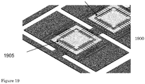
- Figure 19 shows a flexible tape substrate unit 1900 having a second die 1905 attached to the die 1805 of Figure 8 to form a die stack 1910.
- the second die 1905 may be a memory or processor die, by way of non-limiting example.
- the second die 1905 may be implemented and attached to the flexible tape substrate unit 1900 and die 1805 using flip-chip bonding and wire bonding techniques and processes known to those of skill in the art.
- the die attachment may be done at the strip level to increase efficiencies and decrease costs.
- Figure 20 shows a flexible tape substrate unit 2000 having an attached die stack (not visible) that is covered with a mold 2010.
- the mold 2010 may be implemented using mold transfer techniques and processes known to those of skill in the art. The mold transfer may be done at the strip level to increase efficiencies and decrease costs. In addition to covering the die stack, a mold transfer process may be used to cover the SMTs which may provide much better reliability and handling. The temperature may be raised on the molded side for better temperature balance during bonding. Bonding time may then be reduced, which may increase or improve the units per hour (i.e., production).
- Figure 21 shows a bottom or reverse view 2100 of the flexible tape substrate unit 2000.
- an image receiving face or side 2110 of an imager chip 2105 may be visible or exposed to an external light source.
- contact pads 2115 are also shown in Figure 21 for attachment of other components.
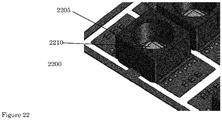
- Figure 22 shows a flexible tape substrate unit 2200 having a housing 2205, by non-limiting example, attached to a bottom or image receiving side 2210.
- the housing 2205 may be used to hold lenses in the case of a camera module, by way of non-limiting example.
- the housing 2205 may be attached to pads (not visible) using techniques and processes known to those of skill in the art. The housing attachment may be done at the strip level to increase efficiencies and decrease costs.
- Figure 23 shows a top or non-image receiving side 2300 of a flexible tape substrate strip 2305 and a flexible tape substrate unit 2310 of the embodiment shown in Figure 22 .
- Figure 24 shows an exploded view 2400 taken along C-C of the flexible tape substrate strip 2300 of Figure 23 .
- Punch singulation may be used to separate the flexible tape substrate unit 910 from the flexible tape substrate strip 900. Punching may be done with the flexible tape substrate as opposed to a snapping or dicing process. Punching is a simpler mechanism and may be used due to the thickness of the flexible tape substrate and strip construction.
- Figure 25 shows a folding process method 2500 for folding a flexible tape substrate unit 2505.
- the flexible tape substrate unit 2505 may have a first end section 2510, a first fold section 2515, a middle section 2520, a second fold section 2525 and a second end section 2530.
- the first end section 2510 and the second end section 2530 are folded toward a top or non-image receiving side 2540 of the flexible tape substrate unit 2505 at a 90° angle (2545).
- the first end section 2510 and the second end section 2530 may then be folded toward each other and cover a stiffener 2550 to form a folded tape package 2555.
- a bottom or image receiving side 2560 of the folded tape package 2555 is also shown.
- more dies may be integrated since the flexible tape substrate is thinner and additional SMTs may be placed internal to the folded tape package 2555 on the first end section 2510 and the second end section 2530.
- Figure 26 shows a top or non-image receiving view of a folded tape package 2600 and Figure 27 shows a bottom or image receiving side of a folded tape package 2700.
- Figure 27 shows a cross-sectional view of a folded tape package 2800 of the folded tape package 2700 along line D-D of Figure 27 .
- an image sensor or imaging chip 2810 is interconnected to a folded tape substrate 2805.
- a processor and/or memory 2820 is interconnected using gold wire 2822 to the image sensor or imaging chip 2810.
- a mold 2825 covers the image sensor or imaging chip 2810 and the processor and/or memory 2820 (i.e., the die stack).
- SMTs 2835 are interconnected to the folded tape substrate 2805.
- a housing 2840 is situated on the bottom or image receiving side of the folded tape substrate 2805.
- Figure 29 is an example flowchart 2900 for manufacturing a folded tape package.
- the folded tape package may be a camera module.
- a 2 layer flexible tape substrate is made using techniques and processes known to those of skill in the art (2905). Flexible tape substrate strips are made where a middle section has a cavity for placement of a die/die stack and two end sections that have, flip-chip bond pads and wire bonding pads on one side of the flexible tape substrate strip and SMT pads and LGA pads on other side of the flexible tape substrate strip (2910). Passive components are mounted on the SMT pads (2915) and a die or die stack is bonded to the flexible tape substrate (2920). A transfer mold process in then applied to the die or die stack and may be applied to the mounted passive components (2925).
- a housing is attached to a non-mold covered die or die stack side (2935).
- the above may all be implemented in strip form.
- Each of the flexible tape substrate units are singulated from the flexible tape substrate strip (2940).
- the end sections of flexible tape substrate units are folded up toward a mold covered die or die stack side and then folded again toward each other such that the end sections are somewhat parallel to the middle section (2945), i.e., the end sections are somewhat parallel to and overlay a mold covered die or die stack.
- the fact that the end sections are described as being somewhat parallel is not to be construed in a limiting manner as they may be disposed as desired.
- Figures 30-44 show another embodiment and process flow for a folded tape package.
- Figure 30 shows an overview of a front end process flow 3000 of the folded tape package.
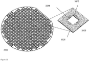
- a silicon substrate or wafer 3005 may have multiple substrate dies 3010, where the wafer 3005 may be processed using techniques and processes known to those of skill in the art.
- Each substrate die 3005 may have flip-chip bonding pads 3015, wire bonding pads 3020 and stud bumps 3025.
- the silicon substrate or wafer may not have warpage issues such as those present for ceramic substrates, have better yield characteristics, and may be back-thinned to any thickness including being less than a ceramic or laminate substrate.
- a functional die or chip such as an imager die or chip 3025, may be flip-chip bonded to each substrate die 3010.
- a processor and/or memory chip or die 3030 may be attached to the imager chip 3025 and wire bonded to the substrate die 3010 to create a die stack 3035.
- the die stack 3035 may be covered with a mold 3040 using a transfer molding process.
- the processing described herein may be done at the wafer level to increase efficiencies and decrease costs.
- the attaching, bonding and transfer molding may use techniques and processes known to those of skill in the art.
- Figure 31 shows an overview of a back end process flow 3100 of the folded tape package.
- Each mold covered die 3110 may be separated from a wafer 3105 using techniques and processes known to those of skill in the art. For example, the wafer may be mounted and sawn to separate the die.
- a flexible tape substrate unit 3115 may be prepared as described herein to include SMT pads 3020, a window cavity 3125, and flip chip pads 3130.
- Passive components 3135 may be attached to the SMT pads 320 to form flexible tape substrate unit 3140.
- the surface mounted passive components may be covered by a mold 3045 using a transfer mold process to form flexible tape substrate unit 3150.
- the mold covered die 3110 may then be flip chip bonded to the flexible tape substrate unit 3150 to form flexible tape substrate unit 3160.
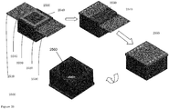
- FIG 32 shows an overview of a tape folding process flow 3200 of the folded tape package.
- a flexible tape substrate unit 3205 may be folded along the dotted lines E-E to form flexible tape substrate unit 3210 and along dotted lines F-F to form flexible tape substrate unit 3215, i.e., the folded tape package.
- the folding process results in flexible tape substrate unit 3215 having an exposed section such that the imager chip 3220 may be exposed to external light and having multiple contact points 3225 for attaching another device, such as a housing 3230, by way of non-limiting example, to form a camera module 3235, by way of non-limiting example.
- Figures 33-37 show an embodiment and process flow for processing a silicon wafer substrate for the folded tape package.
- Figure 33 shows a silicon wafer substrate 3300, where each substrate die 3305 may include flip chip bonds 3310 for placement of a functional die, such as an imager die, by way of non-limiting example, and wire bond pads 3315 for attaching other functional dies, such as a memory and/or processor, by way of non-limiting example.
- the substrate dies 3305 may also include stud bump pads 3320 for attachment to the folding tape substrate.
- Gold sputter plated stud bumps may be applied on each substrate die 3305 using anistropic conductive paste (ACP) bonding process.
- the stud bump may be a single stud bump as opposed to double stud bumps, which may save cost on materials.
- ACP anistropic conductive paste
- stud bumps may not be needed due to the flatness of the wafer and the flexible tape substrate and may reduce costs significantly.
- thermo-compression bonding force may be reduced because bonding on the silicon surface may require less force than the ceramic substrate and also due to the single bump geometry.
- More processing techniques may be used for flip chip bonding such as thermo-sonic bonding. This may occur additionally because of no coefficient of thermal expansion (CTE) mismatch between the dies and substrate. The lack of a mismatch may also increase reliability of the bonding processes.
- the silicon substrate may include embedded passive components. This may save additional area.
- Figure 34 shows attachment of a functional die 3405, such as an imager die, to a silicon wafer substrate 3400 using flip chip bonding processes such as thermo-compression or thermo-sonic flip chip bonding, by way of non-limiting example.
- Figure 35 shows attachment of a functional die 3505, such as a memory and/or processor die, to a first functional die 3510 and attachment of the functional die 3505 to a silicon wafer substrate 3500 using wire bonding 3515 to form a die stack.
- Figure 36 shows the die stack of Figure 35 (not visible) encapsulated with a mold 3605 to form an encapsulated die stack silicon wafer substrate 3600.
- the mold 3605 may be implemented using mold transfer techniques and processes known to those of skill in the art.
- FIG. 36 An exploded view of the studs 3610 as described herein is also shown in Figure 36 . All of the processes described herein above are implemented at a wafer level to increase efficiencies and decrease costs. For example, the units per hour may be significantly improved by processing an 8"wafer with more than 600 units at one time.
- Figure 37 shows a silicon wafer substrate 3700 as processed herein above being mounted and diced into substrate dies 3705 using techniques and processes known to those of skill in the art. Dicing and sawing the silicon may result in less debris than ceramic scoring and snapping. This may lead to better particulate control.
- the separated substrate dies 3705 are then attached to a substrate flexible tape as described herein below.
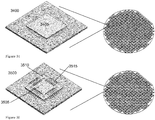
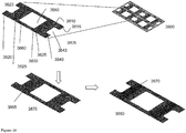
- FIG 38 shows an embodiment of a flexible tape substrate strip 3800 that may have multiple flexible tape substrate units 3805.
- Each flexible tape substrate unit 3805 may have a top surface 3810, (i.e., an image receiving side), and a bottom surface 3815, (i.e., a non-image receiving side).
- Each flexible tape substrate unit 3805 may further have a first end section 3820, a first fold section, 3825, a middle section 3830, a second fold section 3835 and a second end section 3840.
- the first end section 3820 and the second end section 3840 on the top surface 3810 may have multiple surface mount (SMT) pads 3845 for passive components, by way of non-limiting example.
- SMT surface mount
- the first end section 3820 and the second end section 3840 may further include a first notched section 3823 and a second notched section 3843.
- the middle section 3830 may have a window cavity 3850 for the dies, such as the separated substrate dies 3705 in Figure 37 , by way of non-limiting example.
- the window cavity 3850 may have associated flip chip pads 3860.
- the middle section 3850 may have on the bottom surface 3815 LGA pads (not shown).
- the first end section 3820 and the second end section 3840 on the bottom surface 3815 may have contact pads (not shown) for attachment of other devices, such as a housing, by way of non-limiting example.
- the flexible tape substrate and flexible tape substrate strip 3800 may be manufactured, implemented or constructed using techniques and processes known to those of skill in the art. As described herein, the flexible tape substrate may be a high density interconnect (HDI) flexible tape substrate.
- HDI high density interconnect
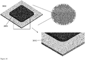
- Surface mounted passive components 3865 may be mounted on flexible tape substrate unit 3805 to form flexible tape substrate unit 3870.
- the placement of the surface mounted passive components 3865 may be accomplished using techniques and processes known to those of skill in the art.
- the surface mounted passive components 3865 may be encapsulated with a mold 3870 to form flexible tape substrate unit 3880. This may increase reliability and handling.
- the mold 3870 may be implemented using mold transfer techniques and processes known to those of skill in the art.
- the temperature may be raised on the molded side for better temperature balance during bonding. Bonding time may then be reduced, which may increase or improve the units per hour (i.e., production).
- the processing described herein for Figure 38 may be done at the strip level to increase efficiencies and decrease costs.
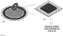
- Figure 39 shows attachment of a processed substrate die 3905 to each processed flexible tape substrate unit in a flexible tape substrate strip 3900 using flip chip bonding processes or techniques as described herein.
- the attachment may be done at the strip level to increase efficiencies and decrease costs.
- Punch singulation may be used to separate a flexible tape substrate unit 3910 from the flexible tape substrate strip 3900.
- Punching may be done with the flexible tape substrate as opposed to a snapping or dicing process. Punching is a simpler mechanism and may be used due to the thickness of the flexible tape substrate and strip construction.
- Figure 40 shows a tape folding process flow 4000 of the folded tape package.
- a singulated flexible tape substrate unit 4005 may be folded along the dotted lines G-G to form flexible tape substrate unit 4010 and along dotted lines H-H to form flexible tape substrate unit 4015, i.e., the folded tape package.
- the folding process results in flexible tape substrate unit 4015 having an exposed section such that the imager chip 4025 may be exposed to external light and having multiple contact points 4030 for attaching another device, such as a housing 4035, by way of non-limiting example, to form a camera module 4040, by way of non-limiting example.
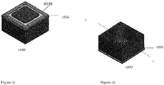
- Figure 41 shows a non-image receiving side 4105 of a folded tape package 4100.
- the LGA pads 4110 as described herein may be seen.
- Figure 42 shows an image receiving side 4205 of a folded tape package 4200.
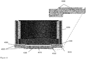
- Figure 43 shows a cross-sectional view of a folded tape package 4300 of the folded tape package 4200 along line I-I of Figure 42 .
- an image sensor or imaging chip 4315 is interconnected to a silicon substrate 4310, which is interconnected to a flexible tape substrate 4305 via gold stud bumps 4350.
- a processor and/or memory 4320 is interconnected to the image sensor 4315 and interconnect to the silicon substrate 4310 using gold wire 4322.
- a mold 4325 covers the image sensor or imaging chip 4315 together with the processor and/or memory 4320 (i.e., the die stack) and the passive components 4330.
- a housing 4335 is situated on the image receiving side of the flexible tape substrate 4305.
- Figure 44 is an example flowchart 4400 for manufacturing a folded tape package.
- the folded tape package may be a camera module.
- a silicon substrate wafer and/or die may be processed to include flip chip bonding pads, wire bonding pads, stud bumps (if needed) and a window cavity for placement of a functional die stack (4405).
- a functional die stack may be attached to the silicon substrate (4410).
- the functional die stack may be encapsulated (4415).
- the die are separated from the wafer using known techniques (4420).
- a flexible tape substrate is made using techniques and processes known to those of skill in the art (4425).
- Flexible tape substrate strips are made where a middle section has a cavity for placement of a die and two end sections that have notches, SMT pads, and flip-chip bond pads on one side of the flexible tape substrate strip and contacts and LGA pads on another side of the flexible tape substrate strip (4430).
- Passive components are mounted on the SMT pads (4435) and encapsulated (4440).
- Encapsulated die may be flip chip mounted to flexible tape substrate units of the flexible tape substrate strip (4445).
- Each of the flexible tape substrate units are singulated from the flexible tape substrate strip (4450).
- the end sections of flexible tape substrate units are folded such that the end sections are somewhat parallel to the middle section (4455), i.e., the end sections are somewhat parallel to and overlay a mold covered die or die stack.
- a housing is attached to an image receiving side (4460).
- the methods described herein are not limited to any particular element(s) that perform(s) any particular function(s) and some steps of the methods presented need not necessarily occur in the order shown. For example, in some cases two or more method steps may occur in a different order or simultaneously. In addition, some steps of the described methods may be optional (even if not explicitly stated to be optional) and, therefore, may be omitted. These and other variations of the methods disclosed herein will be readily apparent, especially in view of the description of the folded tape package described herein.
Landscapes
- Solid State Image Pick-Up Elements (AREA)
- Wire Bonding (AREA)
- Studio Devices (AREA)
Claims (8)
- Kameramodul, das Folgendes umfasst:ein biegsames Substratband (100), umfassend zwei Endabschnitte (120, 140) und einen Mittenabschnitt (130);wobei die zwei Endabschnitte (120, 140) oberflächenmontierte passive Komponenten (210) auf einer oberen Oberfläche (110) des biegsamen Substratbands umfassen;wobei der Mittenabschnitt (130) eine Fensteraussparung (150) für einen Bildgeber-Chipstapel (305, 405) umfasst;und der Mittenabschnitt (130) weiter den Bildgeber-Chipstapel auf der oberen Oberfläche (110) umfasst;wobei der Bildgeber-Chipstapel (305, 405) in einer Form (505) gekapselt ist, sodass eine Bildaufnahmeseite (710, 810) der Fensteraussparung (150) zugewandt freiliegend gelassen ist;wobei die zwei Endabschnitte (120, 140) von dem Mittelabschnitt (130) überlagert und in Richtung der oberen Oberfläche (110) des biegsamen Substratbands (100) umgeklappt sind;sodass sich die zwei Endabschnitte (120, 140) in einer parallelen Konfiguration mit dem Mittenabschnitt (130) befinden; undein Gehäuse (805), das an auf einer unteren Oberfläche (115) des biegsamen Substratbands (100) befindlichen Kontaktpads (715) angebracht ist; wobeidas Gehäuse (805) auf der Bildaufnahmeseite (710, 810) liegt;das Gehäuse (805) auf den Mittenabschnitt (130) und die Bildaufnahmeseite (710, 810) des Bildgeber-Chipstapels (605) ausgerichtet ist; undmindestens die oberflächenmontierten passiven Komponenten (210), der Bildgeber-Chipstapel (305, 405) und das Gehäuse (805) durch das biegsame Substratband (100) elektrisch verbunden sind.
- Kameramodul, das Folgendes umfasst:ein biegsames Substratband (3805), umfassend zwei Endabschnitte (3820, 3840) und einen Mittenabschnitt (3830);wobei die zwei Endabschnitte (3820, 3840) oberflächenmontierte passive Komponenten (3865) auf einer oberen Oberfläche (3810) des biegsamen Substratbands (3805) umfassen;wobei der Mittenabschnitt (3830) eine Fensteraussparung (3850) für einen Bildgeber-Chipstapel (4315, 4320) umfasst; undder Mittenabschnitt weiter den Bildgeber-Chipstapel auf der oberen Oberfläche umfasst;wobei der Bildgeber-Chipstapel in einer Form (3605, 4325) gekapselt ist, sodass eine Bildaufnahmeseite (4205) freiliegend gelassen ist;wobei die zwei Endabschnitte (3820, 3840) jeweils weiter einen eingekerbten Endabschnitt (3823, 3843) umfassen;wobei die zwei Endabschnitte (3820, 3840) in Richtung der oberen Oberfläche (3810) des biegsamen Substratbands umgeklappt sind, um den Mittenabschnitt (3830) zu überlagern und einen freiliegenden Abschnitt beizubehalten, sodass die Bildaufnahmeseite (4205) durch den freiliegenden Abschnitt gegenüber Licht von außen freiliegend gelassen wird;sodass sich die zwei Endabschnitte (3820, 3840) in einer parallelen Konfiguration mit dem Mittenabschnitt (3830) befinden; undein Gehäuse (4035), das an auf einer unteren Oberfläche (3815) des biegsamen Substratbands befindlichen Kontaktpads (4030) angebracht ist; wobeidas Gehäuse (4035) auf der Bildaufnahmeseite (4205) liegt;das Gehäuse (4035) auf den Mittenabschnitt (3830) und die Bildaufnahmeseite (4205) des Bildgeber-Chipstapels ausgerichtet ist; undmindestens die oberflächenmontierten passiven Komponenten (3865), der Bildgeber-Chipstapel und das Gehäuse (4035) durch das biegsame Substratband (3805) elektrisch verbunden sind.
- Kameramodul nach einem der vorangehenden Ansprüche, das weiter Folgendes umfasst:
zwei oder mehr LGA-Pads (720, 4110), die auf der unteren Oberfläche des biegsamen Substratbands montiert sind, und zwei oder mehr Montagepads (145, 3845), die auf der oberen Oberfläche des biegsamen Substratbands montiert sind. - Kameramodul nach einem der Ansprüche 1 bis 3, das weiter Folgendes umfasst:
eine Versteifung (610), die an dem Bildgeber-Chipstapel in der Form angebracht ist. - Kameramodul nach einem der vorangehenden Ansprüche, wobei der von einer Form abgedeckte Bildgeber-Chipstapel weiter Folgendes umfasst:ein Siliziumsubstrat (3005);einen Bildgeber-Chip (3025), der an dem Siliziumsubstrat angebracht ist; undeinen Prozessor und/oder einen Speicher (3030), der an dem Siliziumsubstrat und dem Bildgeber-Chip angebracht ist.
- Verfahren zum Herstellen eines Kameramoduls nach Anspruch 1 oder 2, das Folgendes umfasst:Herstellen eines biegsamen Substratbandstreifens (100, 2800), der biegsame Substratbandeinheiten (105, 3805) aufweist, wobei die obere Oberfläche (110, 3810) der Endabschnitte (120, 140; 3820, 3840) jeder biegsamen Substrateinheit Montagepads für die oberflächenmontierten passiven Komponenten (210, 3865) aufweist und die obere Oberfläche des Mittenabschnitts (130, 3830) jeder der biegsamen Substrateinheiten Pads (145) zum Anschließen des Bildgeber-Chipstapels (305, 405) aufweist;Anbringen der Bildgeber-Chipstapel (305, 405) an dem Mittenabschnitt (130, 3830) jeder biegsamen Substratbandeinheit;Umklappen der Endabschnitte (120, 140; 3820, 3840) in Richtung der oberen Oberfläche (110, 3810), sodass sich die Endabschnitte in einer parallelen Konfiguration mit dem Mittenabschnitt (130, 3830) befinden; undStanzvereinzeln des biegsamen Substratbandstreifens (100, 3800) in die biegsamen Substratbandeinheiten (105, 3805).
- Verfahren nach Anspruch 6, das weiter Folgendes umfasst:Anbringen des Gehäuses (805, 4035) an den auf der biegsamen Substratbandeinheit (105, 3805) befindlichen Kontaktpads,wobei mindestens zwei der Endabschnitt-Montagepads, der Mittenabschnittpads, der Kontaktpads und der auf der unteren Oberfläche des biegsamen Substratbands montierten LGA-Pads elektrisch verbunden sind,wobei das Gehäuse (805, 4035) auf den Mittenabschnitt (130, 3830) ausgerichtet ist.
- Verfahren nach Anspruch 6 oder Anspruch 7, das weiter Folgendes umfasst: Abdecken der montierten passiven Komponenten (210, 3865) mit einer Form; und Anbringen einer Versteifung (610) an dem Bildgeber-Chipstapel.
Applications Claiming Priority (1)
| Application Number | Priority Date | Filing Date | Title |
|---|---|---|---|
| US13/248,593 US8913180B2 (en) | 2011-09-29 | 2011-09-29 | Folded tape package for electronic devices |
Publications (3)
| Publication Number | Publication Date |
|---|---|
| EP2575176A2 EP2575176A2 (de) | 2013-04-03 |
| EP2575176A3 EP2575176A3 (de) | 2013-05-01 |
| EP2575176B1 true EP2575176B1 (de) | 2019-11-20 |
Family
ID=46968053
Family Applications (1)
| Application Number | Title | Priority Date | Filing Date |
|---|---|---|---|
| EP12186417.7A Active EP2575176B1 (de) | 2011-09-29 | 2012-09-27 | Zusammengeklappte Haftbandverpackung für elektronische Vorrichtungen |
Country Status (4)
| Country | Link |
|---|---|
| US (1) | US8913180B2 (de) |
| EP (1) | EP2575176B1 (de) |
| CN (1) | CN103035588B (de) |
| MX (1) | MX2012011218A (de) |
Families Citing this family (4)
| Publication number | Priority date | Publication date | Assignee | Title |
|---|---|---|---|---|
| CN105572840B (zh) * | 2014-11-11 | 2018-11-30 | 信泰光学(深圳)有限公司 | 薄型化光学镜头 |
| CN104409366A (zh) * | 2014-11-19 | 2015-03-11 | 三星半导体(中国)研究开发有限公司 | 芯片封装方法及封装基底 |
| CN109061879A (zh) * | 2018-08-22 | 2018-12-21 | Oppo广东移动通信有限公司 | 光投射器及其破裂的检测方法、深度相机和电子装置 |
| CN111722332B (zh) * | 2020-07-15 | 2023-07-07 | 深圳鹏昱光电科技有限公司 | 一种光模块集成生产系统及其生产方法 |
Citations (1)
| Publication number | Priority date | Publication date | Assignee | Title |
|---|---|---|---|---|
| US6384472B1 (en) * | 2000-03-24 | 2002-05-07 | Siliconware Precision Industries Co., Ltd | Leadless image sensor package structure and method for making the same |
Family Cites Families (12)
| Publication number | Priority date | Publication date | Assignee | Title |
|---|---|---|---|---|
| DE69408558T2 (de) * | 1993-05-28 | 1998-07-23 | Toshiba Ave Kk | Verwendung einer anisotropischen leitfähigen Schicht für die Verbindung von Anschlussleitern einer Leiterplatte mit den elektrischen Anschlusskontakten einer photoelektrischen Umwandlungsvorrichtung und Verfahren zur Montage dieser Vorrichtung |
| JP2001308260A (ja) | 2000-04-25 | 2001-11-02 | Seiko Epson Corp | 半導体装置 |
| JP2001358997A (ja) * | 2000-06-12 | 2001-12-26 | Mitsubishi Electric Corp | 半導体装置 |
| US7246431B2 (en) * | 2002-09-06 | 2007-07-24 | Tessera, Inc. | Methods of making microelectronic packages including folded substrates |
| DE102006046292B9 (de) * | 2006-09-29 | 2014-04-30 | Epcos Ag | Bauelement mit MEMS-Mikrofon und Verfahren zur Herstellung |
| US20080170141A1 (en) * | 2007-01-11 | 2008-07-17 | Samuel Waising Tam | Folded package camera module and method of manufacture |
| JP4900118B2 (ja) * | 2007-07-31 | 2012-03-21 | コニカミノルタオプト株式会社 | カメラモジュールおよび電子機器 |
| JP5313751B2 (ja) * | 2008-05-07 | 2013-10-09 | パナソニック株式会社 | 電子部品装着装置 |
| US8054639B2 (en) | 2008-12-01 | 2011-11-08 | Azurewave Technologies, Inc. | Image-sensing module for reducing overall thickness thereof and preventing EMI |
| US8355628B2 (en) | 2009-03-06 | 2013-01-15 | Visera Technologies Company Limited | Compact camera module |
| JP5281484B2 (ja) | 2009-05-28 | 2013-09-04 | 浜松ホトニクス株式会社 | 放射線検出ユニット |
| US8248523B2 (en) | 2009-11-05 | 2012-08-21 | Flextronics Ap, Llc | Camera module with fold over flexible circuit and cavity substrate |
-
2011
- 2011-09-29 US US13/248,593 patent/US8913180B2/en not_active Expired - Fee Related
-
2012
- 2012-09-27 EP EP12186417.7A patent/EP2575176B1/de active Active
- 2012-09-27 MX MX2012011218A patent/MX2012011218A/es active IP Right Grant
- 2012-09-29 CN CN201210375989.5A patent/CN103035588B/zh not_active Expired - Fee Related
Patent Citations (1)
| Publication number | Priority date | Publication date | Assignee | Title |
|---|---|---|---|---|
| US6384472B1 (en) * | 2000-03-24 | 2002-05-07 | Siliconware Precision Industries Co., Ltd | Leadless image sensor package structure and method for making the same |
Also Published As
| Publication number | Publication date |
|---|---|
| CN103035588B (zh) | 2017-07-28 |
| CN103035588A (zh) | 2013-04-10 |
| EP2575176A2 (de) | 2013-04-03 |
| MX2012011218A (es) | 2013-07-12 |
| US8913180B2 (en) | 2014-12-16 |
| US20130083239A1 (en) | 2013-04-04 |
| EP2575176A3 (de) | 2013-05-01 |
Similar Documents
| Publication | Publication Date | Title |
|---|---|---|
| US8791536B2 (en) | Stacked sensor packaging structure and method | |
| JP6102941B2 (ja) | 光学装置及びその製造方法 | |
| US7315078B2 (en) | Chip-stacked semiconductor package and method for fabricating the same | |
| US8378478B2 (en) | Enhanced stacked microelectronic assemblies with central contacts and vias connected to the central contacts | |
| US7867821B1 (en) | Integrated circuit package system with through semiconductor vias and method of manufacture thereof | |
| US8553420B2 (en) | Enhanced stacked microelectronic assemblies with central contacts and improved thermal characteristics | |
| US6917090B2 (en) | Chip scale image sensor package | |
| EP1686628A2 (de) | Bildaufnahmesensorverpackung und ihr Herstellungsverfahren | |
| US9635228B2 (en) | Image sensors with interconnects in cover layer | |
| US20080283971A1 (en) | Semiconductor Device and Its Fabrication Method | |
| JP7444850B2 (ja) | 半導体装置、撮像装置および半導体装置の製造方法 | |
| EP2575176B1 (de) | Zusammengeklappte Haftbandverpackung für elektronische Vorrichtungen | |
| JP2005294443A (ja) | 半導体装置及びその製造方法 | |
| US20130001757A1 (en) | Flip-chip qfn structure using etched lead frame | |
| JP4494240B2 (ja) | 樹脂封止型半導体装置 | |
| US10109660B2 (en) | Laminated semiconductor device | |
| KR20160031523A (ko) | 피막을 통과하여 연장되는 커넥터에 의하여 커플링되는 적층 단자를 가지는 마이크로전자 어셈블리 | |
| EP1093165A1 (de) | Zusammenbau hochintegrierter Schaltungen | |
| US20260052987A1 (en) | Semiconductor packages and semiconductor devices comprising heat transfer member |
Legal Events
| Date | Code | Title | Description |
|---|---|---|---|
| PUAL | Search report despatched |
Free format text: ORIGINAL CODE: 0009013 |
|
| PUAI | Public reference made under article 153(3) epc to a published international application that has entered the european phase |
Free format text: ORIGINAL CODE: 0009012 |
|
| AK | Designated contracting states |
Kind code of ref document: A2 Designated state(s): AL AT BE BG CH CY CZ DE DK EE ES FI FR GB GR HR HU IE IS IT LI LT LU LV MC MK MT NL NO PL PT RO RS SE SI SK SM TR |
|
| AX | Request for extension of the european patent |
Extension state: BA ME |
|
| AK | Designated contracting states |
Kind code of ref document: A3 Designated state(s): AL AT BE BG CH CY CZ DE DK EE ES FI FR GB GR HR HU IE IS IT LI LT LU LV MC MK MT NL NO PL PT RO RS SE SI SK SM TR |
|
| AX | Request for extension of the european patent |
Extension state: BA ME |
|
| RIC1 | Information provided on ipc code assigned before grant |
Ipc: H01L 27/146 20060101AFI20130325BHEP |
|
| 17P | Request for examination filed |
Effective date: 20131101 |
|
| RBV | Designated contracting states (corrected) |
Designated state(s): AL AT BE BG CH CY CZ DE DK EE ES FI FR GB GR HR HU IE IS IT LI LT LU LV MC MK MT NL NO PL PT RO RS SE SI SK SM TR |
|
| 17Q | First examination report despatched |
Effective date: 20131129 |
|
| GRAP | Despatch of communication of intention to grant a patent |
Free format text: ORIGINAL CODE: EPIDOSNIGR1 |
|
| STAA | Information on the status of an ep patent application or granted ep patent |
Free format text: STATUS: GRANT OF PATENT IS INTENDED |
|
| INTG | Intention to grant announced |
Effective date: 20190521 |
|
| GRAS | Grant fee paid |
Free format text: ORIGINAL CODE: EPIDOSNIGR3 |
|
| GRAJ | Information related to disapproval of communication of intention to grant by the applicant or resumption of examination proceedings by the epo deleted |
Free format text: ORIGINAL CODE: EPIDOSDIGR1 |
|
| GRAL | Information related to payment of fee for publishing/printing deleted |
Free format text: ORIGINAL CODE: EPIDOSDIGR3 |
|
| STAA | Information on the status of an ep patent application or granted ep patent |
Free format text: STATUS: EXAMINATION IS IN PROGRESS |
|
| GRAJ | Information related to disapproval of communication of intention to grant by the applicant or resumption of examination proceedings by the epo deleted |
Free format text: ORIGINAL CODE: EPIDOSDIGR1 |
|
| GRAP | Despatch of communication of intention to grant a patent |
Free format text: ORIGINAL CODE: EPIDOSNIGR1 |
|
| GRAR | Information related to intention to grant a patent recorded |
Free format text: ORIGINAL CODE: EPIDOSNIGR71 |
|
| STAA | Information on the status of an ep patent application or granted ep patent |
Free format text: STATUS: GRANT OF PATENT IS INTENDED |
|
| GRAA | (expected) grant |
Free format text: ORIGINAL CODE: 0009210 |
|
| STAA | Information on the status of an ep patent application or granted ep patent |
Free format text: STATUS: THE PATENT HAS BEEN GRANTED |
|
| INTC | Intention to grant announced (deleted) | ||
| RAP1 | Party data changed (applicant data changed or rights of an application transferred) |
Owner name: FLEXTRONICS AP, LLC |
|
| AK | Designated contracting states |
Kind code of ref document: B1 Designated state(s): AL AT BE BG CH CY CZ DE DK EE ES FI FR GB GR HR HU IE IS IT LI LT LU LV MC MK MT NL NO PL PT RO RS SE SI SK SM TR |
|
| INTG | Intention to grant announced |
Effective date: 20191011 |
|
| REG | Reference to a national code |
Ref country code: GB Ref legal event code: FG4D |
|
| REG | Reference to a national code |
Ref country code: CH Ref legal event code: EP |
|
| REG | Reference to a national code |
Ref country code: IE Ref legal event code: FG4D |
|
| REG | Reference to a national code |
Ref country code: DE Ref legal event code: R096 Ref document number: 602012065775 Country of ref document: DE |
|
| REG | Reference to a national code |
Ref country code: AT Ref legal event code: REF Ref document number: 1205166 Country of ref document: AT Kind code of ref document: T Effective date: 20191215 |
|
| REG | Reference to a national code |
Ref country code: NL Ref legal event code: MP Effective date: 20191120 |
|
| REG | Reference to a national code |
Ref country code: LT Ref legal event code: MG4D |
|
| PG25 | Lapsed in a contracting state [announced via postgrant information from national office to epo] |
Ref country code: NL Free format text: LAPSE BECAUSE OF FAILURE TO SUBMIT A TRANSLATION OF THE DESCRIPTION OR TO PAY THE FEE WITHIN THE PRESCRIBED TIME-LIMIT Effective date: 20191120 Ref country code: LV Free format text: LAPSE BECAUSE OF FAILURE TO SUBMIT A TRANSLATION OF THE DESCRIPTION OR TO PAY THE FEE WITHIN THE PRESCRIBED TIME-LIMIT Effective date: 20191120 Ref country code: SE Free format text: LAPSE BECAUSE OF FAILURE TO SUBMIT A TRANSLATION OF THE DESCRIPTION OR TO PAY THE FEE WITHIN THE PRESCRIBED TIME-LIMIT Effective date: 20191120 Ref country code: ES Free format text: LAPSE BECAUSE OF FAILURE TO SUBMIT A TRANSLATION OF THE DESCRIPTION OR TO PAY THE FEE WITHIN THE PRESCRIBED TIME-LIMIT Effective date: 20191120 Ref country code: NO Free format text: LAPSE BECAUSE OF FAILURE TO SUBMIT A TRANSLATION OF THE DESCRIPTION OR TO PAY THE FEE WITHIN THE PRESCRIBED TIME-LIMIT Effective date: 20200220 Ref country code: GR Free format text: LAPSE BECAUSE OF FAILURE TO SUBMIT A TRANSLATION OF THE DESCRIPTION OR TO PAY THE FEE WITHIN THE PRESCRIBED TIME-LIMIT Effective date: 20200221 Ref country code: LT Free format text: LAPSE BECAUSE OF FAILURE TO SUBMIT A TRANSLATION OF THE DESCRIPTION OR TO PAY THE FEE WITHIN THE PRESCRIBED TIME-LIMIT Effective date: 20191120 Ref country code: BG Free format text: LAPSE BECAUSE OF FAILURE TO SUBMIT A TRANSLATION OF THE DESCRIPTION OR TO PAY THE FEE WITHIN THE PRESCRIBED TIME-LIMIT Effective date: 20200220 Ref country code: FI Free format text: LAPSE BECAUSE OF FAILURE TO SUBMIT A TRANSLATION OF THE DESCRIPTION OR TO PAY THE FEE WITHIN THE PRESCRIBED TIME-LIMIT Effective date: 20191120 |
|
| PG25 | Lapsed in a contracting state [announced via postgrant information from national office to epo] |
Ref country code: RS Free format text: LAPSE BECAUSE OF FAILURE TO SUBMIT A TRANSLATION OF THE DESCRIPTION OR TO PAY THE FEE WITHIN THE PRESCRIBED TIME-LIMIT Effective date: 20191120 Ref country code: IS Free format text: LAPSE BECAUSE OF FAILURE TO SUBMIT A TRANSLATION OF THE DESCRIPTION OR TO PAY THE FEE WITHIN THE PRESCRIBED TIME-LIMIT Effective date: 20200320 Ref country code: HR Free format text: LAPSE BECAUSE OF FAILURE TO SUBMIT A TRANSLATION OF THE DESCRIPTION OR TO PAY THE FEE WITHIN THE PRESCRIBED TIME-LIMIT Effective date: 20191120 |
|
| PG25 | Lapsed in a contracting state [announced via postgrant information from national office to epo] |
Ref country code: AL Free format text: LAPSE BECAUSE OF FAILURE TO SUBMIT A TRANSLATION OF THE DESCRIPTION OR TO PAY THE FEE WITHIN THE PRESCRIBED TIME-LIMIT Effective date: 20191120 |
|
| PG25 | Lapsed in a contracting state [announced via postgrant information from national office to epo] |
Ref country code: DK Free format text: LAPSE BECAUSE OF FAILURE TO SUBMIT A TRANSLATION OF THE DESCRIPTION OR TO PAY THE FEE WITHIN THE PRESCRIBED TIME-LIMIT Effective date: 20191120 Ref country code: PT Free format text: LAPSE BECAUSE OF FAILURE TO SUBMIT A TRANSLATION OF THE DESCRIPTION OR TO PAY THE FEE WITHIN THE PRESCRIBED TIME-LIMIT Effective date: 20200412 Ref country code: EE Free format text: LAPSE BECAUSE OF FAILURE TO SUBMIT A TRANSLATION OF THE DESCRIPTION OR TO PAY THE FEE WITHIN THE PRESCRIBED TIME-LIMIT Effective date: 20191120 Ref country code: RO Free format text: LAPSE BECAUSE OF FAILURE TO SUBMIT A TRANSLATION OF THE DESCRIPTION OR TO PAY THE FEE WITHIN THE PRESCRIBED TIME-LIMIT Effective date: 20191120 Ref country code: CZ Free format text: LAPSE BECAUSE OF FAILURE TO SUBMIT A TRANSLATION OF THE DESCRIPTION OR TO PAY THE FEE WITHIN THE PRESCRIBED TIME-LIMIT Effective date: 20191120 |
|
| REG | Reference to a national code |
Ref country code: AT Ref legal event code: MK05 Ref document number: 1205166 Country of ref document: AT Kind code of ref document: T Effective date: 20191120 |
|
| REG | Reference to a national code |
Ref country code: DE Ref legal event code: R097 Ref document number: 602012065775 Country of ref document: DE |
|
| PG25 | Lapsed in a contracting state [announced via postgrant information from national office to epo] |
Ref country code: SK Free format text: LAPSE BECAUSE OF FAILURE TO SUBMIT A TRANSLATION OF THE DESCRIPTION OR TO PAY THE FEE WITHIN THE PRESCRIBED TIME-LIMIT Effective date: 20191120 Ref country code: SM Free format text: LAPSE BECAUSE OF FAILURE TO SUBMIT A TRANSLATION OF THE DESCRIPTION OR TO PAY THE FEE WITHIN THE PRESCRIBED TIME-LIMIT Effective date: 20191120 |
|
| PLBE | No opposition filed within time limit |
Free format text: ORIGINAL CODE: 0009261 |
|
| STAA | Information on the status of an ep patent application or granted ep patent |
Free format text: STATUS: NO OPPOSITION FILED WITHIN TIME LIMIT |
|
| 26N | No opposition filed |
Effective date: 20200821 |
|
| PG25 | Lapsed in a contracting state [announced via postgrant information from national office to epo] |
Ref country code: PL Free format text: LAPSE BECAUSE OF FAILURE TO SUBMIT A TRANSLATION OF THE DESCRIPTION OR TO PAY THE FEE WITHIN THE PRESCRIBED TIME-LIMIT Effective date: 20191120 Ref country code: SI Free format text: LAPSE BECAUSE OF FAILURE TO SUBMIT A TRANSLATION OF THE DESCRIPTION OR TO PAY THE FEE WITHIN THE PRESCRIBED TIME-LIMIT Effective date: 20191120 Ref country code: AT Free format text: LAPSE BECAUSE OF FAILURE TO SUBMIT A TRANSLATION OF THE DESCRIPTION OR TO PAY THE FEE WITHIN THE PRESCRIBED TIME-LIMIT Effective date: 20191120 |
|
| PG25 | Lapsed in a contracting state [announced via postgrant information from national office to epo] |
Ref country code: MC Free format text: LAPSE BECAUSE OF FAILURE TO SUBMIT A TRANSLATION OF THE DESCRIPTION OR TO PAY THE FEE WITHIN THE PRESCRIBED TIME-LIMIT Effective date: 20191120 |
|
| REG | Reference to a national code |
Ref country code: CH Ref legal event code: PL |
|
| REG | Reference to a national code |
Ref country code: BE Ref legal event code: MM Effective date: 20200930 |
|
| PG25 | Lapsed in a contracting state [announced via postgrant information from national office to epo] |
Ref country code: LU Free format text: LAPSE BECAUSE OF NON-PAYMENT OF DUE FEES Effective date: 20200927 |
|
| PG25 | Lapsed in a contracting state [announced via postgrant information from national office to epo] |
Ref country code: LI Free format text: LAPSE BECAUSE OF NON-PAYMENT OF DUE FEES Effective date: 20200930 Ref country code: IE Free format text: LAPSE BECAUSE OF NON-PAYMENT OF DUE FEES Effective date: 20200927 Ref country code: BE Free format text: LAPSE BECAUSE OF NON-PAYMENT OF DUE FEES Effective date: 20200930 Ref country code: CH Free format text: LAPSE BECAUSE OF NON-PAYMENT OF DUE FEES Effective date: 20200930 |
|
| PG25 | Lapsed in a contracting state [announced via postgrant information from national office to epo] |
Ref country code: TR Free format text: LAPSE BECAUSE OF FAILURE TO SUBMIT A TRANSLATION OF THE DESCRIPTION OR TO PAY THE FEE WITHIN THE PRESCRIBED TIME-LIMIT Effective date: 20191120 Ref country code: MT Free format text: LAPSE BECAUSE OF FAILURE TO SUBMIT A TRANSLATION OF THE DESCRIPTION OR TO PAY THE FEE WITHIN THE PRESCRIBED TIME-LIMIT Effective date: 20191120 Ref country code: CY Free format text: LAPSE BECAUSE OF FAILURE TO SUBMIT A TRANSLATION OF THE DESCRIPTION OR TO PAY THE FEE WITHIN THE PRESCRIBED TIME-LIMIT Effective date: 20191120 |
|
| PG25 | Lapsed in a contracting state [announced via postgrant information from national office to epo] |
Ref country code: MK Free format text: LAPSE BECAUSE OF FAILURE TO SUBMIT A TRANSLATION OF THE DESCRIPTION OR TO PAY THE FEE WITHIN THE PRESCRIBED TIME-LIMIT Effective date: 20191120 |
|
| PGFP | Annual fee paid to national office [announced via postgrant information from national office to epo] |
Ref country code: IT Payment date: 20230920 Year of fee payment: 12 Ref country code: GB Payment date: 20230926 Year of fee payment: 12 |
|
| PGFP | Annual fee paid to national office [announced via postgrant information from national office to epo] |
Ref country code: FR Payment date: 20230926 Year of fee payment: 12 Ref country code: DE Payment date: 20230928 Year of fee payment: 12 |
|
| REG | Reference to a national code |
Ref country code: DE Ref legal event code: R079 Ref document number: 602012065775 Country of ref document: DE Free format text: PREVIOUS MAIN CLASS: H01L0027146000 Ipc: H10F0039180000 |
|
| REG | Reference to a national code |
Ref country code: DE Ref legal event code: R119 Ref document number: 602012065775 Country of ref document: DE |
|
| GBPC | Gb: european patent ceased through non-payment of renewal fee |
Effective date: 20240927 |
|
| PG25 | Lapsed in a contracting state [announced via postgrant information from national office to epo] |
Ref country code: DE Free format text: LAPSE BECAUSE OF NON-PAYMENT OF DUE FEES Effective date: 20250401 |
|
| PG25 | Lapsed in a contracting state [announced via postgrant information from national office to epo] |
Ref country code: GB Free format text: LAPSE BECAUSE OF NON-PAYMENT OF DUE FEES Effective date: 20240927 |
|
| PG25 | Lapsed in a contracting state [announced via postgrant information from national office to epo] |
Ref country code: IT Free format text: LAPSE BECAUSE OF NON-PAYMENT OF DUE FEES Effective date: 20240927 |
|
| PG25 | Lapsed in a contracting state [announced via postgrant information from national office to epo] |
Ref country code: FR Free format text: LAPSE BECAUSE OF NON-PAYMENT OF DUE FEES Effective date: 20240930 |