EP2560286A2 - System und Verfahren zum Reduzieren oder Eliminieren der Temperaturunabhängigkeit eines kohärenten Empfängers in einer drahtlosen Kommunikationsvorrichtung - Google Patents
System und Verfahren zum Reduzieren oder Eliminieren der Temperaturunabhängigkeit eines kohärenten Empfängers in einer drahtlosen Kommunikationsvorrichtung Download PDFInfo
- Publication number
- EP2560286A2 EP2560286A2 EP12178040A EP12178040A EP2560286A2 EP 2560286 A2 EP2560286 A2 EP 2560286A2 EP 12178040 A EP12178040 A EP 12178040A EP 12178040 A EP12178040 A EP 12178040A EP 2560286 A2 EP2560286 A2 EP 2560286A2
- Authority
- EP
- European Patent Office
- Prior art keywords
- current
- temperature
- wireless communication
- receiver
- bias
- Prior art date
- Legal status (The legal status is an assumption and is not a legal conclusion. Google has not performed a legal analysis and makes no representation as to the accuracy of the status listed.)
- Granted
Links
Images


Classifications
-
- H—ELECTRICITY
- H04—ELECTRIC COMMUNICATION TECHNIQUE
- H04B—TRANSMISSION
- H04B1/00—Details of transmission systems, not covered by a single one of groups H04B3/00 - H04B13/00; Details of transmission systems not characterised by the medium used for transmission
- H04B1/02—Transmitters
- H04B1/04—Circuits
- H04B1/0475—Circuits with means for limiting noise, interference or distortion
Definitions
- the present disclosure relates generally to wireless communication and, more particularly, to reducing or eliminating temperature dependence of a coherent receiver in a wireless communication device.
- Wireless communications systems are used in a variety of telecommunications systems, television, radio and other media systems, data communication networks, and other systems to convey information between remote points using wireless transmitters and wireless receivers.
- a transmitter is an electronic device which, usually with the aid of an antenna, propagates an electromagnetic signal such as radio, television, or other telecommunications. Transmitters often include digital signal processing circuits which encode a data signal, upconverts it to a radio frequency signal, and passes it signal amplifiers which receive the radio-frequency, amplify the signal by a predetermined gain, and transmit the amplified signal through an antenna.
- a receiver is an electronic device which, also usually with the aid of an antenna, receives and processes a wireless electromagnetic signal. In certain instances, a transmitter and receiver may be combined into a single device called a transceiver.
- a wireless communication device may include, in addition to a transmitter and a receiver, a coherent receiver as part of a feedback control path for monitoring and control of the transmitter.
- a feedback control path may provide for monitoring of a phase shift in a transmit path, an output power intensity of a transmit path, and/or other parameters.
- the control path may control operational parameters in order to provide desired behavior within the transmit path.
- the gain characteristics of the feedback control path must remain substantially constant over temperature.
- a method may include generating a first current equal to a bandgap voltage divided by a resistance selected to approximately match a process resistance integral to a receiver.
- the method may further include generating a second current equal to temperature-dependent current multiplied by a predetermined scaling factor.
- the method may also include subtracting the second current from the first current to generate a bias current.
- the method may additionally include providing the bias current to the receiver.
- a bias circuit comprising; a bias reference current portion configured to generate a first current equal to a bandgap voltage divided by a resistance selected to approximately match a process resistance integral to a receiver; a temperature reference current portion configured to generate a second current equal to temperature-dependent current multiplied by a predetermined scaling factor; and a mirroring portion configured to generate a bias current equal to the first current minus the second current.
- FIGURE 1 illustrates a block diagram of an example wireless communication system 100, in accordance with certain embodiments of the present disclosure.
- a terminal 110 may also be referred to as a remote station, a mobile station, an access terminal, user equipment (UE), a wireless communication device, a cellular phone, or some other terminology.
- a base station 120 may be a fixed station and may also be referred to as an access point, a Node B, or some other terminology.
- a terminal 110 may or may not be capable of receiving signals from satellites 130.
- Satellites 130 may belong to a satellite positioning system such as the well-known Global Positioning System (GPS).
- GPS Global Positioning System
- Each GPS satellite may transmit a GPS signal encoded with information that allows GPS receivers on earth to measure the time of arrival of the GPS signal. Measurements for a sufficient number of GPS satellites may be used to accurately estimate a three-dimensional position of a GPS receiver.
- a terminal 110 may also be capable of receiving signals from other types of transmitting sources such as a Bluetooth transmitter, a Wireless Fidelity (Wi-Fi) transmitter, a wireless local area network (WLAN) transmitter, an IEEE 802.11 transmitter, and any other suitable transmitter.
- Wi-Fi Wireless Fidelity
- WLAN wireless local area network
- IEEE 802.11 transmitter any other suitable transmitter.
- each terminal 110 is shown as receiving signals from multiple transmitting sources simultaneously, where a transmitting source may be a base station 120 or a satellite 130. In certain embodiments, a terminal 110 may also be a transmitting source. In general, a terminal 110 may receive signals from zero, one, or multiple transmitting sources at any given moment.
- System 100 may be a Code Division Multiple Access (CDMA) system, a Time Division Multiple Access (TDMA) system, or some other wireless communication system.
- CDMA Code Division Multiple Access
- TDMA Time Division Multiple Access
- a CDMA system may implement one or more CDMA standards such as IS-95, IS-2000 (also commonly known as “1x”), IS-856 (also commonly known as “1xEV-DO"), Wideband-CDMA (W-CDMA), and so on.
- a TDMA system may implement one or more TDMA standards such as Global System for Mobile Communications (GSM).
- GSM Global System for Mobile Communications
- the W-CDMA standard is defined by a consortium known as 3GPP
- the IS-2000 and IS-856 standards are defined by a consortium known as 3GPP2.
- FIGURE 2 illustrates a block diagram of selected components of an example transmitting and/or receiving element 200 (e.g., a terminal 110, a base station 120, or a satellite 130), in accordance with certain embodiments of the present disclosure.
- Element 200 may include a transmit path 201, a receive path 221, and a feedback control path 241.
- element 200 may be considered a transmitter, a receiver, or a transceiver.
- element 200 may include digital circuitry 202.
- Digital circuitry 202 may include any system, device, or apparatus configured to process digital signals and information received via receive path 221 and/or feedback control path 241, and/or configured to process signals and information for transmission via transmit path 201.
- Such digital circuitry 202 may include one or more microprocessors, digital signal processors, and/or other suitable devices.
- digital circuitry 202 may communicate in-phase (I) channel and quadrature (Q) channel components of a digital signal to transmit path 201.
- Transmit path 201 may include a digital-to-analog converter (DAC) 204 for each of the I channel and Q channel signals communicated by digital circuitry 202.
- DAC digital-to-analog converter
- Each DAC 204 may be configured to receive its respective I or Q channel component of the digital signal from digital circuitry 202 and convert such digital signal into an analog signal. Such analog signal may then be passed to one or more other components of transmit path 201, including upconverter 208.
- Upconverter 208 may be configured to frequency upconvert an analog signal received from DAC 204 to a wireless communication signal at a radio frequency based on an oscillator signal provided by oscillator 210.
- Oscillator 210 may be any suitable device, system, or apparatus configured to produce an analog waveform of a particular frequency for modulation or upconversion of an analog signal to a wireless communication signal, or for demodulation or downconversion of a wireless communication signal to an analog signal.
- oscillator 210 may be a digitally-controlled crystal oscillator.
- Transmit path 201 may include a variable-gain amplifier (VGA) 214 to amplify an upconverted signal for transmission, and a power amplifier 220 to further amplify the analog upconverted signal for transmission via antenna 218.
- VGA variable-gain amplifier
- the output of power amplifier 220 may be communicated to duplexer 223.
- a duplexer 223 may be interfaced between antenna switch 216 and each transmit path 201 and receive path 221. Accordingly, duplexer 223 may allow bidirectional communication through antenna 218 (e.g., from transmit path 201 to antenna 218, and from antenna 218 to receive path 221).
- Antenna switch 216 may be coupled between duplexer 224 and antenna 218.
- Antenna switch 216 may configured to multiplex the output of two or more power amplifiers (e.g., similar to power amplifier 220), in which each power amplifier may correspond to a different band or band class.
- Antenna switch 216 may allow duplexing of signals received by antenna 218 to a plurality of receive paths of different bands or band classes.
- Antenna 218 may receive the amplified signal from antenna switch 216 (e.g., via RF coupler 242) and transmit such signal (e.g., to one or more of a terminal 110, a base station 120, and/or a satellite 130). As shown in FIGURE 2 , antenna 218 may be coupled to each of transmit path 201 and receive path 221.
- Receive path 221 may include a low-noise amplifier 234 configured to receive a wireless communication signal (e.g., from a terminal 110, a base station 120, and/or a satellite 130) via antenna 218, antenna tuner 217, and duplexer 223.
- LNA 234 may be further configured to amplify the received signal.
- Receive path 221 may also include a downconverter 228.
- Downconverter 228 may be configured to frequency downconvert a wireless communication signal received via antenna 218 and amplified by LNA 234 by an oscillator signal provided by oscillator 210 (e.g., downconvert to a baseband signal).
- Receive path 221 may further include a filter 238, which may be configured to filter a downconverted wireless communication signal in order to pass the signal components within a radio-frequency channel of interest and/or to remove noise and undesired signals that may be generated by the downconversion process.
- receive path 221 may include an analog-to-digital converter (ADC) 224 configured to receive an analog signal from filter 238 and convert such analog signal into a digital signal. Such digital signal may then be passed to digital circuitry 202 for processing.
- ADC analog-to-digital converter
- Feedback control path 241 may in general be configured to monitor one or more parameters of transmit path 201 (e.g, gain, phase shift, etc.), and transmit a digital signal indicative of such parameters to digital circuitry 202 for analysis and/or control of transmit path 201. For example, based on monitored parameters, digital circuitry may modify I channel and Q channel signals communicated to transmit path 202, modify gain parameters of components of transmit path 201, and/or may take other actions.
- parameters of transmit path 201 e.g, gain, phase shift, etc.
- digital circuitry may modify I channel and Q channel signals communicated to transmit path 202, modify gain parameters of components of transmit path 201, and/or may take other actions.
- feedback control path 241 may include a radio frequency (RF) coupler 242.
- RF coupler 242 may be any system, device or apparatus configured to couple at least a portion of the transmission power in the transmission line coupling antenna switch 216 to antenna 218 to one or more output ports.
- one of the output ports may be known as a coupled port (e.g., coupled port 246 as shown in FIGURE 2 ) while the other output port may be known as a terminated or isolated port (e.g., terminated port 247 as shown in FIGURE 2 ).
- each of coupled port 246 and terminated port 247 may be terminated with an internal or external resistance of a particular resistance value (e.g., 50 ohms).
- coupled port 246 may carry an analog signal (e.g., a voltage) indicative of incident power transmitted to antenna 218 while terminated port 247 may carry an analog signal (e.g., a voltage) indicative of power reflected from antenna 218.
- analog signal e.g., a voltage
- terminated port 247 may carry an analog signal (e.g., a voltage) indicative of power reflected from antenna 218.
- Feedback control path 241 may include a variable gain amplifier (VGA) 254 to amplify signals communicated from RF coupler 242, and communicate such amplified signals to downconverter/amplifier 248.
- VGA variable gain amplifier
- Downconverter/amplifier 248 may be configured to frequency downconvert the analog signal received from VGA 254 by an oscillator signal provided by oscillator 210 (e.g., downconvert to a baseband signal) and output an in-phase (I) channel and quadrature (Q) channel components of for the signal.
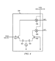
- An example embodiment of downconverter/amplifier 248 is shown in FIGURE 4 .
- control path 214 may include an analog-to-digital converter (ADC) 244 for each of the I channel and Q channel, each ADC 244 configured to receive the appropriate component of the baseband signal convert such components of the signal into a digital components of the signal.
- the digital components of the signal output by ADCs 244 may be communicated to digital circuitry 202 for processing. Together, VGA 254, downconverter 246, ADCs 244, and/or other components may make up a coherent receiver coherent to transmit path 201.
- FIGURE 3 illustrates a block diagram of certain components of feedback control path 241, along with a biasing circuit 302 for certain components of feedback control path 241.
- FIGURE 3 depicts a signal path within feedback control path 241 for only one channel of a signal , rather than both the in-phase and quadrature channel.
- analog-to-digital converter 244 may be implemented using a summer 302, a loop filter 304, and a feedback DAC 306.
- Summer 302 may be any system, device, or apparatus configured to sum an analog signal from the output of downconverter/amplifier 248 to an analog signal from the output of feedback DAC 306.
- Loop filter 304 may be any system, device, or apparatus configured to, in connection with summer 302 and feedback DAC 306, convert an analog signal received from downconverter/amplifier 248 into a digital signal indicative of the received analog signal.
- Loop filter 304 may be implemented as an integrator, delta-sigma modulator, and/or any other suitable circuit.
- Feedback DAC 306 may be configured to convert the digital output of loop filter 304 into an analog signal to be subtracted by summer 302 from the analog signal received from downconverter 302. As shown in FIGURE 3 , biasing circuit 302 may provide a bias current to feedback DAC 306, thus enabling functionality of feedback DAC 306. As described in greater detail below, biasing circuit 302 may be configured to generate a bias current to offset variations of other components of feedback control path 241 (e.g., downconverter/amplifier 248) due to temperature.
- feedback control path 241 e.g., downconverter/amplifier 248
- FIGURE 4 illustrates a block diagram of selected components of an example downconverter/amplifier 248, in accordance with certain embodiments of the present disclosure.
- downconverter/amplifier 248 may include transistors 402 and resistors 404 having resistance R arranged to form a resistively-generated amplifier.
- downconverter/amplifier 248 may include mixers 406 to downconvert an RF signal to baseband.
- downconverter/amplifier 248 may not include mixers 406.
- a signal gain Gm of downconverter/amplifier 248 may be proportional to the quantity Vbg / R - PTAT*k, where Vbg is a bandgap voltage supplied to provide a bias current to downconverter/amplifier 248, R is a process-dependent resistance present in downconverter/amplifier 248 (e.g., a resistor 404 shown in FIGURE 4 ), PTAT is a temperature-dependent current, and k is a scalar constant based on physical characteristics of downconverter/amplifier 248.
- bias circuit 302 may be configured to generate a temperature-dependent bias current.
- bias circuit 302 may include summers 310 and 312, switches 311, op amp 314, mirrored transistors 316 (e.g., transistors 316a and 316b), resistor 318, current proportional to ambient temperature circuits (PTATs) 322, and temperature-independent current circuits (ZTCs) 324.
- mirrored transistors 316 e.g., transistors 316a and 316b
- resistor 318 current proportional to ambient temperature circuits (PTATs) 322, and temperature-independent current circuits (ZTCs) 324.
- a PTAT 322 may comprise any system, device, or apparatus configured to generate an electrical current proportional to an ambient temperature present proximate to such PTAT 322, wherein such electrical current is also a function of a predetermined scaling factor n .
- the scaling factor n may be set by an adjustable trim (e.g., by adjusting a resistance of a variable resistor or potentiometer) based on characterization of feedback control path 241, as described in greater detail below.
- a ZTC 324 may comprise any system, device, or apparatus configured to generate an electrical current independent of an ambient temperature present proximate to such ZTC 324, wherein such electrical current is also a function of a predetermined scaling factor n .
- Each summer 310 may comprise any system, device, or apparatus configured to subtract a current generated by a ZTC 324 from a current generated by a PTAT 322, thus outputting an electrical current that is dependent upon temperature and the scaling factor n , wherein such electrical current will be approximately zero at a particular temperature.
- PTATs 322 and/or ZTCs 324 may be configured such that the particular temperature is a desired temperature (e.g., room temperature of approximately 27 degrees Celsius).
- Switches 311 and summer 312 may be configured such that the output of summer 312 either sources an electrical current output by a summer 310 or sinks an electrical current output by a summer 310, resulting in an electrical current that may be represented by the quantity PTAT* n .
- Operational amplifier 314 may comprise any system, device, or apparatus with a differential input and either a single-ended or differential output (a single-ended output is depicted in FIGURE 3 ), which is a multiple of the voltage difference between the input terminals.
- the negative input terminal of operational amplifier 314 may be supplied with a bandgap voltage Vbg, while the positive input terminal may be coupled to the output of summer 312, a resistor 318, and an active-region terminal (e.g., source, drain, emitter, collector) of a mirrored transistor 316a.
- the output terminal may be coupled to gates of each of mirrored transistors 316.
- Mirrored transistors 316 may include any suitable transistor.
- Transistors 316 are depicted in the specific embodiment of FIGURE 3 as n-type metal-oxide semiconductor field-effect transistors (MOSFETs). As shown in FIGURE 3 , transistors 316 may be coupled to each other and to a rail voltage (e.g., VDD) at one of their active-region terminals (e.g., source, drain, emitter, collector) and coupled to each other and the output of operational amplifier 314 at their non-active-region terminals (e.g., base, collector).
- VDD rail voltage
- mirrored transistors 316 form a current mirror, such that a current sourced by and flowing through the various terminals of transistor 316b is approximately equal to the current sourced by and flowing through the various terminals of transistor 316a.
- Resistor 318 may include any suitable resistive circuit element.
- resistor 318 may be selected to have a resistance R based on a process resistance present in downconverter/amplifier 248 and/or other components of feedback control path 241.
- resistor 318 may be coupled between the positive input terminal of operational amplifier 316 and a rail voltage (e.g., VSS).
- VSS rail voltage
- Those of skill in the art may appreciate that, as so configured, the voltage present at the positive input terminal of operational amplifier 314, and thus the voltage present at node A, will be approximately equal to Vbg. Accordingly, an electrical current flowing through resistor 318 will be approximately equal to Vbg / R.
- the current flowing through transistor 316a may be approximately equal to Vbg / R - PTAT* n .
- Transistor 316b may mirror the current of transistor 316a, and such current may be provided as a bias current to ADC 244 (e.g., as a bias current to feedback DAC 306).
- the bias current provided to feedback DAC 306 and/or other components of ADC 244 may be approximately centered about Vbg / R, and vary linearly with temperature as a function of the scaling factor n .
- the output current of feedback DAC 306 may be proportional to the bias current, and thus, is a function of temperature, as given in the PTAT* n term of the bias current.
- performance of other components of feedback control path 241 may vary with temperature.
- a gain Gm of downconverter/amplifier 248 may have temperature dependence and may be proportional to the quantity Vbg / R - PTAT* k , where k is a constant scaling factor based on physical properties of downconverter/amplifier 248.
- an output current generated by downconverter/amplifier 248 may also have temperature dependence and may be proportional to the quantity Vbg / R - PTAT* k .
- temperature variance of downconverter/amplifier 248 and/or other components of feedback control path 241 may be offset, reduced, or eliminated if a suitable value for scaling factor n is selected.
- a manufacturer or other individual may select an appropriate value of n , such that feedback control path 241 may operate with little or no temperature dependence.
- system 100 may be integrated or separated. Moreover, the operations of system 100 may be performed by more, fewer, or other components. As used in this document, "each" refers to each member of a set or each member of a subset of a set.
Landscapes
- Engineering & Computer Science (AREA)
- Computer Networks & Wireless Communication (AREA)
- Signal Processing (AREA)
- Amplifiers (AREA)
- Transceivers (AREA)
- Superheterodyne Receivers (AREA)
- Circuits Of Receivers In General (AREA)
Applications Claiming Priority (1)
| Application Number | Priority Date | Filing Date | Title |
|---|---|---|---|
| US13/208,190 US8489044B2 (en) | 2011-08-11 | 2011-08-11 | System and method for reducing or eliminating temperature dependence of a coherent receiver in a wireless communication device |
Publications (3)
| Publication Number | Publication Date |
|---|---|
| EP2560286A2 true EP2560286A2 (de) | 2013-02-20 |
| EP2560286A3 EP2560286A3 (de) | 2017-08-09 |
| EP2560286B1 EP2560286B1 (de) | 2018-11-07 |
Family
ID=46796259
Family Applications (1)
| Application Number | Title | Priority Date | Filing Date |
|---|---|---|---|
| EP12178040.7A Active EP2560286B1 (de) | 2011-08-11 | 2012-07-26 | System und Verfahren zum Reduzieren oder Eliminieren der Temperaturunabhängigkeit eines kohärenten Empfängers in einer drahtlosen Kommunikationsvorrichtung |
Country Status (4)
| Country | Link |
|---|---|
| US (1) | US8489044B2 (de) |
| EP (1) | EP2560286B1 (de) |
| JP (1) | JP5778096B2 (de) |
| CN (1) | CN102957647B (de) |
Families Citing this family (7)
| Publication number | Priority date | Publication date | Assignee | Title |
|---|---|---|---|---|
| WO2013016575A2 (en) | 2011-07-28 | 2013-01-31 | Skyworks Solutions, Inc. | Low variation current multiplier |
| FR2979160B1 (fr) * | 2011-08-16 | 2013-09-06 | Mobilead | Dispositif de preparation de code a lecture optique |
| US20150280946A1 (en) * | 2014-03-27 | 2015-10-01 | Qualcomm Incorporated | Feedback receive path with low-if mode |
| US9704591B2 (en) * | 2014-12-17 | 2017-07-11 | Sandisk Technologies Llc | Temperature independent reference current generation for calibration |
| US20160179113A1 (en) * | 2014-12-17 | 2016-06-23 | Sandisk Technologies Inc. | Temperature Independent Reference Current Generation For Calibration |
| TWI703813B (zh) * | 2019-04-23 | 2020-09-01 | 瑞昱半導體股份有限公司 | 訊號補償裝置 |
| US12072722B2 (en) * | 2022-06-24 | 2024-08-27 | Analog Devices, Inc. | Bias current with hybrid temperature profile |
Family Cites Families (28)
| Publication number | Priority date | Publication date | Assignee | Title |
|---|---|---|---|---|
| US4243948A (en) | 1979-05-08 | 1981-01-06 | Rca Corporation | Substantially temperature-independent trimming of current flows |
| US4590418A (en) * | 1984-11-05 | 1986-05-20 | General Motors Corporation | Circuit for generating a temperature stabilized reference voltage |
| US5125112A (en) | 1990-09-17 | 1992-06-23 | Motorola, Inc. | Temperature compensated current source |
| JPH0529841A (ja) * | 1991-07-23 | 1993-02-05 | Mitsubishi Electric Corp | 温度補償付き増幅回路 |
| US5920808A (en) * | 1996-12-12 | 1999-07-06 | Glenayre Electronics, Inc. | Method and apparatus for reducing key-up distortion by pre-heating transistors |
| US6265857B1 (en) | 1998-12-22 | 2001-07-24 | International Business Machines Corporation | Constant current source circuit with variable temperature compensation |
| CH697322B1 (fr) * | 2000-06-13 | 2008-08-15 | Em Microelectronic Marin Sa | Procédé de génération d'un courant sensiblement indépendent de la température et dispositif permettant de mettre en oeuvre ce procédé. |
| JP2002094394A (ja) * | 2000-09-19 | 2002-03-29 | Matsushita Electric Ind Co Ltd | 送信装置及び送信出力制御方法 |
| US6340882B1 (en) * | 2000-10-03 | 2002-01-22 | International Business Machines Corporation | Accurate current source with an adjustable temperature dependence circuit |
| US6614305B1 (en) | 2002-02-19 | 2003-09-02 | Texas Instruments Incorporated | Method and circuit for trimming offset and temperature drift for operational amplifiers and voltage references |
| US6664847B1 (en) * | 2002-10-10 | 2003-12-16 | Texas Instruments Incorporated | CTAT generator using parasitic PNP device in deep sub-micron CMOS process |
| US6819164B1 (en) | 2002-10-17 | 2004-11-16 | National Semiconductor Corporation | Apparatus and method for a precision bi-directional trim scheme |
| JP2005027130A (ja) * | 2003-07-04 | 2005-01-27 | Renesas Technology Corp | 高周波電力増幅回路のバイアス制御回路および高周波電力増幅用電子部品 |
| US6911861B2 (en) | 2003-08-07 | 2005-06-28 | Texas Instruments Incorporated | Current biasing circuit with temperature compensation and related methods of compensating output current |
| US7081796B2 (en) * | 2003-09-15 | 2006-07-25 | Silicon Laboratories, Inc. | Radio frequency low noise amplifier with automatic gain control |
| US6967526B1 (en) | 2004-02-20 | 2005-11-22 | Maxim Integrated Products, Inc. | Low temperature coefficient input offset voltage trim with digital control |
| CA2513956A1 (en) | 2004-07-27 | 2006-01-27 | Sachdev Manjo | Adjustable and programmable temperature coefficient - proportional to absolute temperature (aptc-ptat) circuit |
| US7439601B2 (en) * | 2004-09-14 | 2008-10-21 | Agere Systems Inc. | Linear integrated circuit temperature sensor apparatus with adjustable gain and offset |
| US7406269B2 (en) * | 2006-03-10 | 2008-07-29 | Discovery Semiconductors, Inc. | Feedback-controlled coherent optical receiver with electrical compensation/equalization |
| US7288983B1 (en) * | 2006-08-30 | 2007-10-30 | Broadlight Ltd. | Method and circuit for providing a temperature dependent current source |
| KR100862475B1 (ko) | 2007-01-25 | 2008-10-08 | 삼성전기주식회사 | 가변 온도계수를 갖는 바이어스 전류 생성 장치 |
| US7780346B2 (en) * | 2007-10-31 | 2010-08-24 | Texas Instruments Incorporated | Methods and apparatus for a fully isolated NPN based temperature detector |
| CN101453270B (zh) * | 2007-12-04 | 2013-04-24 | 无锡江南计算技术研究所 | 激光驱动器及其温度补偿电路 |
| JP5031535B2 (ja) * | 2007-12-04 | 2012-09-19 | 株式会社リコー | 温度検出回路 |
| TWI367412B (en) * | 2008-09-08 | 2012-07-01 | Faraday Tech Corp | Rrecision voltage and current reference circuit |
| JP5107272B2 (ja) * | 2009-01-15 | 2012-12-26 | 株式会社東芝 | 温度補償回路 |
| DE102009040543B4 (de) | 2009-09-08 | 2014-02-13 | Texas Instruments Deutschland Gmbh | Schaltung und Verfahren zum Trimmen einer Offsetdrift |
| CN102064773B (zh) * | 2009-11-16 | 2013-09-11 | 杭州士兰微电子股份有限公司 | 可调增益低噪声放大器 |
-
2011
- 2011-08-11 US US13/208,190 patent/US8489044B2/en active Active
-
2012
- 2012-07-26 EP EP12178040.7A patent/EP2560286B1/de active Active
- 2012-08-08 JP JP2012176087A patent/JP5778096B2/ja active Active
- 2012-08-13 CN CN201210291038.XA patent/CN102957647B/zh active Active
Non-Patent Citations (1)
| Title |
|---|
| None |
Also Published As
| Publication number | Publication date |
|---|---|
| CN102957647B (zh) | 2018-04-10 |
| CN102957647A (zh) | 2013-03-06 |
| JP5778096B2 (ja) | 2015-09-16 |
| EP2560286A3 (de) | 2017-08-09 |
| EP2560286B1 (de) | 2018-11-07 |
| JP2013042493A (ja) | 2013-02-28 |
| US20130039394A1 (en) | 2013-02-14 |
| US8489044B2 (en) | 2013-07-16 |
Similar Documents
| Publication | Publication Date | Title |
|---|---|---|
| EP2560286B1 (de) | System und Verfahren zum Reduzieren oder Eliminieren der Temperaturunabhängigkeit eines kohärenten Empfängers in einer drahtlosen Kommunikationsvorrichtung | |
| CN107749768B (zh) | 用于调谐无线通信设备中的天线的系统和方法 | |
| CN111527694B (zh) | 具有互补单元结构的差分放大器 | |
| US8922178B2 (en) | Temperature dependent voltage regulator | |
| US9608586B2 (en) | Voltage-to-current converter | |
| US8493127B1 (en) | System and method for linearization of a mixer | |
| US20200083847A1 (en) | System and method for biasing an amplifier | |
| US8868022B2 (en) | Broadband transconductance amplifier | |
| CN102857452A (zh) | 用于估算和校正无线通信设备中的相位偏移的系统和方法 | |
| US8526905B2 (en) | Merged filter-transconductor-upconverter | |
| US20120206209A1 (en) | System and Method for Reducing Temperature-and Process-Dependent Frequency Variation of a Crystal Oscillator Circuit | |
| US8364112B2 (en) | Linearization technique for mixer | |
| US12418269B2 (en) | Circuit and method for biasing an amplifier | |
| WO2023076197A1 (en) | Circuit and method for biasing an amplifier | |
| US8451046B2 (en) | System and method for switch leakage cancellation | |
| US20250096839A1 (en) | Oscillator Leakage Calibration | |
| US20240272661A1 (en) | Voltage-to-Current Conversion | |
| US12255586B2 (en) | Oscillator feedthrough calibration | |
| US20250392321A1 (en) | Bias circuit for an active phase shifter | |
| CN120604455A (zh) | 电压到电流转换 |
Legal Events
| Date | Code | Title | Description |
|---|---|---|---|
| PUAI | Public reference made under article 153(3) epc to a published international application that has entered the european phase |
Free format text: ORIGINAL CODE: 0009012 |
|
| AK | Designated contracting states |
Kind code of ref document: A2 Designated state(s): AL AT BE BG CH CY CZ DE DK EE ES FI FR GB GR HR HU IE IS IT LI LT LU LV MC MK MT NL NO PL PT RO RS SE SI SK SM TR |
|
| AX | Request for extension of the european patent |
Extension state: BA ME |
|
| RAP1 | Party data changed (applicant data changed or rights of an application transferred) |
Owner name: INTEL IP CORPORATION |
|
| PUAL | Search report despatched |
Free format text: ORIGINAL CODE: 0009013 |
|
| AK | Designated contracting states |
Kind code of ref document: A3 Designated state(s): AL AT BE BG CH CY CZ DE DK EE ES FI FR GB GR HR HU IE IS IT LI LT LU LV MC MK MT NL NO PL PT RO RS SE SI SK SM TR |
|
| AX | Request for extension of the european patent |
Extension state: BA ME |
|
| RIC1 | Information provided on ipc code assigned before grant |
Ipc: H04B 1/04 20060101AFI20170704BHEP |
|
| STAA | Information on the status of an ep patent application or granted ep patent |
Free format text: STATUS: REQUEST FOR EXAMINATION WAS MADE |
|
| 17P | Request for examination filed |
Effective date: 20180209 |
|
| RBV | Designated contracting states (corrected) |
Designated state(s): AL AT BE BG CH CY CZ DE DK EE ES FI FR GB GR HR HU IE IS IT LI LT LU LV MC MK MT NL NO PL PT RO RS SE SI SK SM TR |
|
| GRAP | Despatch of communication of intention to grant a patent |
Free format text: ORIGINAL CODE: EPIDOSNIGR1 |
|
| STAA | Information on the status of an ep patent application or granted ep patent |
Free format text: STATUS: GRANT OF PATENT IS INTENDED |
|
| INTG | Intention to grant announced |
Effective date: 20180612 |
|
| GRAS | Grant fee paid |
Free format text: ORIGINAL CODE: EPIDOSNIGR3 |
|
| GRAA | (expected) grant |
Free format text: ORIGINAL CODE: 0009210 |
|
| STAA | Information on the status of an ep patent application or granted ep patent |
Free format text: STATUS: THE PATENT HAS BEEN GRANTED |
|
| AK | Designated contracting states |
Kind code of ref document: B1 Designated state(s): AL AT BE BG CH CY CZ DE DK EE ES FI FR GB GR HR HU IE IS IT LI LT LU LV MC MK MT NL NO PL PT RO RS SE SI SK SM TR |
|
| REG | Reference to a national code |
Ref country code: GB Ref legal event code: FG4D |
|
| REG | Reference to a national code |
Ref country code: CH Ref legal event code: EP Ref country code: AT Ref legal event code: REF Ref document number: 1063306 Country of ref document: AT Kind code of ref document: T Effective date: 20181115 |
|
| REG | Reference to a national code |
Ref country code: IE Ref legal event code: FG4D |
|
| REG | Reference to a national code |
Ref country code: DE Ref legal event code: R096 Ref document number: 602012053094 Country of ref document: DE |
|
| REG | Reference to a national code |
Ref country code: NL Ref legal event code: MP Effective date: 20181107 |
|
| REG | Reference to a national code |
Ref country code: LT Ref legal event code: MG4D |
|
| REG | Reference to a national code |
Ref country code: AT Ref legal event code: MK05 Ref document number: 1063306 Country of ref document: AT Kind code of ref document: T Effective date: 20181107 |
|
| PG25 | Lapsed in a contracting state [announced via postgrant information from national office to epo] |
Ref country code: FI Free format text: LAPSE BECAUSE OF FAILURE TO SUBMIT A TRANSLATION OF THE DESCRIPTION OR TO PAY THE FEE WITHIN THE PRESCRIBED TIME-LIMIT Effective date: 20181107 Ref country code: AT Free format text: LAPSE BECAUSE OF FAILURE TO SUBMIT A TRANSLATION OF THE DESCRIPTION OR TO PAY THE FEE WITHIN THE PRESCRIBED TIME-LIMIT Effective date: 20181107 Ref country code: LT Free format text: LAPSE BECAUSE OF FAILURE TO SUBMIT A TRANSLATION OF THE DESCRIPTION OR TO PAY THE FEE WITHIN THE PRESCRIBED TIME-LIMIT Effective date: 20181107 Ref country code: HR Free format text: LAPSE BECAUSE OF FAILURE TO SUBMIT A TRANSLATION OF THE DESCRIPTION OR TO PAY THE FEE WITHIN THE PRESCRIBED TIME-LIMIT Effective date: 20181107 Ref country code: LV Free format text: LAPSE BECAUSE OF FAILURE TO SUBMIT A TRANSLATION OF THE DESCRIPTION OR TO PAY THE FEE WITHIN THE PRESCRIBED TIME-LIMIT Effective date: 20181107 Ref country code: NO Free format text: LAPSE BECAUSE OF FAILURE TO SUBMIT A TRANSLATION OF THE DESCRIPTION OR TO PAY THE FEE WITHIN THE PRESCRIBED TIME-LIMIT Effective date: 20190207 Ref country code: IS Free format text: LAPSE BECAUSE OF FAILURE TO SUBMIT A TRANSLATION OF THE DESCRIPTION OR TO PAY THE FEE WITHIN THE PRESCRIBED TIME-LIMIT Effective date: 20190307 Ref country code: ES Free format text: LAPSE BECAUSE OF FAILURE TO SUBMIT A TRANSLATION OF THE DESCRIPTION OR TO PAY THE FEE WITHIN THE PRESCRIBED TIME-LIMIT Effective date: 20181107 Ref country code: BG Free format text: LAPSE BECAUSE OF FAILURE TO SUBMIT A TRANSLATION OF THE DESCRIPTION OR TO PAY THE FEE WITHIN THE PRESCRIBED TIME-LIMIT Effective date: 20190207 |
|
| PG25 | Lapsed in a contracting state [announced via postgrant information from national office to epo] |
Ref country code: AL Free format text: LAPSE BECAUSE OF FAILURE TO SUBMIT A TRANSLATION OF THE DESCRIPTION OR TO PAY THE FEE WITHIN THE PRESCRIBED TIME-LIMIT Effective date: 20181107 Ref country code: NL Free format text: LAPSE BECAUSE OF FAILURE TO SUBMIT A TRANSLATION OF THE DESCRIPTION OR TO PAY THE FEE WITHIN THE PRESCRIBED TIME-LIMIT Effective date: 20181107 Ref country code: PT Free format text: LAPSE BECAUSE OF FAILURE TO SUBMIT A TRANSLATION OF THE DESCRIPTION OR TO PAY THE FEE WITHIN THE PRESCRIBED TIME-LIMIT Effective date: 20190307 Ref country code: SE Free format text: LAPSE BECAUSE OF FAILURE TO SUBMIT A TRANSLATION OF THE DESCRIPTION OR TO PAY THE FEE WITHIN THE PRESCRIBED TIME-LIMIT Effective date: 20181107 Ref country code: RS Free format text: LAPSE BECAUSE OF FAILURE TO SUBMIT A TRANSLATION OF THE DESCRIPTION OR TO PAY THE FEE WITHIN THE PRESCRIBED TIME-LIMIT Effective date: 20181107 Ref country code: GR Free format text: LAPSE BECAUSE OF FAILURE TO SUBMIT A TRANSLATION OF THE DESCRIPTION OR TO PAY THE FEE WITHIN THE PRESCRIBED TIME-LIMIT Effective date: 20190208 |
|
| PG25 | Lapsed in a contracting state [announced via postgrant information from national office to epo] |
Ref country code: CZ Free format text: LAPSE BECAUSE OF FAILURE TO SUBMIT A TRANSLATION OF THE DESCRIPTION OR TO PAY THE FEE WITHIN THE PRESCRIBED TIME-LIMIT Effective date: 20181107 Ref country code: PL Free format text: LAPSE BECAUSE OF FAILURE TO SUBMIT A TRANSLATION OF THE DESCRIPTION OR TO PAY THE FEE WITHIN THE PRESCRIBED TIME-LIMIT Effective date: 20181107 Ref country code: DK Free format text: LAPSE BECAUSE OF FAILURE TO SUBMIT A TRANSLATION OF THE DESCRIPTION OR TO PAY THE FEE WITHIN THE PRESCRIBED TIME-LIMIT Effective date: 20181107 Ref country code: IT Free format text: LAPSE BECAUSE OF FAILURE TO SUBMIT A TRANSLATION OF THE DESCRIPTION OR TO PAY THE FEE WITHIN THE PRESCRIBED TIME-LIMIT Effective date: 20181107 |
|
| REG | Reference to a national code |
Ref country code: DE Ref legal event code: R097 Ref document number: 602012053094 Country of ref document: DE |
|
| PG25 | Lapsed in a contracting state [announced via postgrant information from national office to epo] |
Ref country code: SK Free format text: LAPSE BECAUSE OF FAILURE TO SUBMIT A TRANSLATION OF THE DESCRIPTION OR TO PAY THE FEE WITHIN THE PRESCRIBED TIME-LIMIT Effective date: 20181107 Ref country code: RO Free format text: LAPSE BECAUSE OF FAILURE TO SUBMIT A TRANSLATION OF THE DESCRIPTION OR TO PAY THE FEE WITHIN THE PRESCRIBED TIME-LIMIT Effective date: 20181107 Ref country code: EE Free format text: LAPSE BECAUSE OF FAILURE TO SUBMIT A TRANSLATION OF THE DESCRIPTION OR TO PAY THE FEE WITHIN THE PRESCRIBED TIME-LIMIT Effective date: 20181107 Ref country code: SM Free format text: LAPSE BECAUSE OF FAILURE TO SUBMIT A TRANSLATION OF THE DESCRIPTION OR TO PAY THE FEE WITHIN THE PRESCRIBED TIME-LIMIT Effective date: 20181107 |
|
| PLBE | No opposition filed within time limit |
Free format text: ORIGINAL CODE: 0009261 |
|
| STAA | Information on the status of an ep patent application or granted ep patent |
Free format text: STATUS: NO OPPOSITION FILED WITHIN TIME LIMIT |
|
| REG | Reference to a national code |
Ref country code: NL Ref legal event code: NE Effective date: 20190930 |
|
| 26N | No opposition filed |
Effective date: 20190808 |
|
| PG25 | Lapsed in a contracting state [announced via postgrant information from national office to epo] |
Ref country code: SI Free format text: LAPSE BECAUSE OF FAILURE TO SUBMIT A TRANSLATION OF THE DESCRIPTION OR TO PAY THE FEE WITHIN THE PRESCRIBED TIME-LIMIT Effective date: 20181107 |
|
| PG25 | Lapsed in a contracting state [announced via postgrant information from national office to epo] |
Ref country code: MC Free format text: LAPSE BECAUSE OF FAILURE TO SUBMIT A TRANSLATION OF THE DESCRIPTION OR TO PAY THE FEE WITHIN THE PRESCRIBED TIME-LIMIT Effective date: 20181107 |
|
| REG | Reference to a national code |
Ref country code: CH Ref legal event code: PL |
|
| PG25 | Lapsed in a contracting state [announced via postgrant information from national office to epo] |
Ref country code: TR Free format text: LAPSE BECAUSE OF FAILURE TO SUBMIT A TRANSLATION OF THE DESCRIPTION OR TO PAY THE FEE WITHIN THE PRESCRIBED TIME-LIMIT Effective date: 20181107 |
|
| REG | Reference to a national code |
Ref country code: BE Ref legal event code: MM Effective date: 20190731 |
|
| PG25 | Lapsed in a contracting state [announced via postgrant information from national office to epo] |
Ref country code: LI Free format text: LAPSE BECAUSE OF NON-PAYMENT OF DUE FEES Effective date: 20190731 Ref country code: CH Free format text: LAPSE BECAUSE OF NON-PAYMENT OF DUE FEES Effective date: 20190731 Ref country code: LU Free format text: LAPSE BECAUSE OF NON-PAYMENT OF DUE FEES Effective date: 20190726 Ref country code: BE Free format text: LAPSE BECAUSE OF NON-PAYMENT OF DUE FEES Effective date: 20190731 |
|
| REG | Reference to a national code |
Ref country code: DE Ref legal event code: R082 Ref document number: 602012053094 Country of ref document: DE Representative=s name: WITHERS & ROGERS LLP, DE Ref country code: DE Ref legal event code: R081 Ref document number: 602012053094 Country of ref document: DE Owner name: APPLE INC., CUPERTINO, US Free format text: FORMER OWNER: INTEL IP CORPORATION, SANTA CLARA, CALIF., US Ref country code: DE Ref legal event code: R081 Ref document number: 602012053094 Country of ref document: DE Owner name: APPLE INC., CUPERTINO, US Free format text: FORMER OWNER: INTEL IP CORPORATION, SANTA CLARA, CA, US |
|
| PG25 | Lapsed in a contracting state [announced via postgrant information from national office to epo] |
Ref country code: IE Free format text: LAPSE BECAUSE OF NON-PAYMENT OF DUE FEES Effective date: 20190726 |
|
| REG | Reference to a national code |
Ref country code: GB Ref legal event code: 732E Free format text: REGISTERED BETWEEN 20201029 AND 20201104 |
|
| PG25 | Lapsed in a contracting state [announced via postgrant information from national office to epo] |
Ref country code: CY Free format text: LAPSE BECAUSE OF FAILURE TO SUBMIT A TRANSLATION OF THE DESCRIPTION OR TO PAY THE FEE WITHIN THE PRESCRIBED TIME-LIMIT Effective date: 20181107 |
|
| PG25 | Lapsed in a contracting state [announced via postgrant information from national office to epo] |
Ref country code: HU Free format text: LAPSE BECAUSE OF FAILURE TO SUBMIT A TRANSLATION OF THE DESCRIPTION OR TO PAY THE FEE WITHIN THE PRESCRIBED TIME-LIMIT; INVALID AB INITIO Effective date: 20120726 Ref country code: MT Free format text: LAPSE BECAUSE OF FAILURE TO SUBMIT A TRANSLATION OF THE DESCRIPTION OR TO PAY THE FEE WITHIN THE PRESCRIBED TIME-LIMIT Effective date: 20181107 |
|
| PG25 | Lapsed in a contracting state [announced via postgrant information from national office to epo] |
Ref country code: MK Free format text: LAPSE BECAUSE OF FAILURE TO SUBMIT A TRANSLATION OF THE DESCRIPTION OR TO PAY THE FEE WITHIN THE PRESCRIBED TIME-LIMIT Effective date: 20181107 |
|
| PGFP | Annual fee paid to national office [announced via postgrant information from national office to epo] |
Ref country code: GB Payment date: 20250605 Year of fee payment: 14 |
|
| PGFP | Annual fee paid to national office [announced via postgrant information from national office to epo] |
Ref country code: FR Payment date: 20250610 Year of fee payment: 14 |
|
| PGFP | Annual fee paid to national office [announced via postgrant information from national office to epo] |
Ref country code: DE Payment date: 20250604 Year of fee payment: 14 |