EP2553811B1 - Circuit de détection et procédé pour faire fonctionner un circuit de détection - Google Patents
Circuit de détection et procédé pour faire fonctionner un circuit de détection Download PDFInfo
- Publication number
- EP2553811B1 EP2553811B1 EP11707645.5A EP11707645A EP2553811B1 EP 2553811 B1 EP2553811 B1 EP 2553811B1 EP 11707645 A EP11707645 A EP 11707645A EP 2553811 B1 EP2553811 B1 EP 2553811B1
- Authority
- EP
- European Patent Office
- Prior art keywords
- signal
- detection
- circuit
- switch
- short
- Prior art date
- Legal status (The legal status is an assumption and is not a legal conclusion. Google has not performed a legal analysis and makes no representation as to the accuracy of the status listed.)
- Not-in-force
Links
- 238000001514 detection method Methods 0.000 title claims description 102
- 238000000034 method Methods 0.000 title claims description 5
- 238000001914 filtration Methods 0.000 claims description 4
- 239000004065 semiconductor Substances 0.000 claims description 4
- 230000000052 comparative effect Effects 0.000 claims 1
- 238000005259 measurement Methods 0.000 description 15
- 230000003071 parasitic effect Effects 0.000 description 4
- 239000003990 capacitor Substances 0.000 description 3
- 230000000694 effects Effects 0.000 description 3
- 230000007613 environmental effect Effects 0.000 description 3
- 230000002452 interceptive effect Effects 0.000 description 2
- 230000001960 triggered effect Effects 0.000 description 2
- 208000010201 Exanthema Diseases 0.000 description 1
- 230000000295 complement effect Effects 0.000 description 1
- 230000001419 dependent effect Effects 0.000 description 1
- 238000011161 development Methods 0.000 description 1
- 230000018109 developmental process Effects 0.000 description 1
- 201000005884 exanthem Diseases 0.000 description 1
- 229910044991 metal oxide Inorganic materials 0.000 description 1
- 150000004706 metal oxides Chemical class 0.000 description 1
- 238000012544 monitoring process Methods 0.000 description 1
- 206010037844 rash Diseases 0.000 description 1
Images
Classifications
-
- G—PHYSICS
- G01—MEASURING; TESTING
- G01R—MEASURING ELECTRIC VARIABLES; MEASURING MAGNETIC VARIABLES
- G01R1/00—Details of instruments or arrangements of the types included in groups G01R5/00 - G01R13/00 and G01R31/00
- G01R1/30—Structural combination of electric measuring instruments with basic electronic circuits, e.g. with amplifier
-
- H—ELECTRICITY
- H03—ELECTRONIC CIRCUITRY
- H03K—PULSE TECHNIQUE
- H03K17/00—Electronic switching or gating, i.e. not by contact-making and –breaking
- H03K17/08—Modifications for protecting switching circuit against overcurrent or overvoltage
- H03K17/082—Modifications for protecting switching circuit against overcurrent or overvoltage by feedback from the output to the control circuit
- H03K17/0822—Modifications for protecting switching circuit against overcurrent or overvoltage by feedback from the output to the control circuit in field-effect transistor switches
-
- H—ELECTRICITY
- H03—ELECTRONIC CIRCUITRY
- H03K—PULSE TECHNIQUE
- H03K2217/00—Indexing scheme related to electronic switching or gating, i.e. not by contact-making or -breaking covered by H03K17/00
- H03K2217/0027—Measuring means of, e.g. currents through or voltages across the switch
Definitions
- switches are used which switch an output terminal against a supply voltage or a reference potential.
- These low-side (NPN) or high-side switches (PNP) are power electronic integrated circuits with additional protection and monitoring functions.
- a high-side switch switches a positive supply voltage
- a low-side switch a negative supply voltage
- a sensor state is signaled.
- the switch is closed when a sensor detects something and open if the sensor does not detect.
- both low-side and high-side switches are able to drive some 100 mA and have an output resistance of less than 10 ⁇ .
- Another function of the switches includes protecting a sensor from short circuits. If, for example, a short-circuit is detected by a suitable short-circuit detection circuit, then a low-side or high-side switch causes a load to be switched off for a specific time interval (about 100 ms). After this switch-off time, a further detection of a short circuit and, if appropriate, a switch-off of the load takes place for a further time interval. Typically, these shutdown times are programmable and may represent, for example, 100 ms, 200 ms, or any other suitable value.
- a short circuit must be detected with high accuracy. This serves to protect the sensors.
- the short-circuit protection also serves to protect a complete system in which the sensor is installed.
- EMC Electromagnetic Compatibility
- CMOS Complementary Metal Oxide Semiconductor
- a short circuit is indicated by the detection circuit when the voltage at the node is too high and thus exceeds, for example, a predetermined comparison value.
- a corresponding switch such as a transistor, will then open or close the switch, thus disconnecting a load from a supply voltage, for example.
- typical switches such as transistors have a parasitic diode effect.
- EMC signals or voltages thus have a clearly asymmetric signal curve and have a negative or positive rash. Again, these signals may be sufficient to indicate a short circuit event, even if it is not present.
- the patent US 5,898,554 shows a driver circuit for a semiconductor power switch. This has a control terminal and a switchable current path and also includes means connected to the control terminal are to provide a voltage to the control terminal. Further, means are provided connected to the switchable current path for detecting a short circuit condition and means responsive to a detected short circuit condition for shutting down the voltage on the control terminal. In this case, the means responding to a detected short-circuit condition are designed for linearly shutting down the voltage on the control connection and for preventing a large voltage spike via the switchable current path.
- the object of the invention is therefore to provide a detection circuit which can detect a short circuit with improved accuracy.
- a detection circuit comprises a detection path and a control path.
- the detection path includes a signal limiter with a signal input connected to a detection node. Furthermore, the detection path has a filter which is coupled to a signal output of the signal limiter.
- a short-circuit detector has a first and a second detector input and a detector output. In this case, the first detector input is coupled to the filter.
- the control path includes a control circuit for controlling a switch.
- the control circuit By means of a control input, the control circuit is coupled to the detector output and the filter.
- a control output of the control circuit is connected to the switch.
- the switch in turn is coupled to the detection node and a supply node.
- a sensor can be connected to the detection node. If, for example, a short circuit occurs on this sensor that could destroy the sensor, a signal characteristic of this event is present at the detection node.
- This signal is first supplied to the signal limiter in the sequence.
- the signal limiter is adapted to limit the signal amplitude of the signal to a measurement interval which is adjustable by means of a threshold value, wherein the threshold value determines the middle of the measurement interval. In this way, the signal limiter generates an intermediate signal, which is fed to the filter.
- the filter in turn filters the intermediate signal to a filtered intermediate rule signal.
- the filtered pre-processed intermediate signal is then applied to the short-circuit detector or to the first detector input.
- Short-circuit detector is configured to detect a short-circuit event from the filtered intermediate signal and to correspondingly generate a control signal, which is fed via the detector output to the control circuit or the control input.
- control circuit switches the switch. If the short-circuit detector detects a short circuit, the control signal causes the switch to close or open and a connected load to be disconnected from a supply voltage.
- a signal at the detection node can be suitably limited by the signal limiter. If, for example, undesired signals, which are harmless to a sensor, are present at the detection node, this can be taken into account by the signal limiter. Larger and temporally limited deflections due to pulses and signal peaks do not lead to the detection of a short circuit in this way.
- the signal amplitude can be limited upwards or downwards.
- the downstream filter it is also possible to set characteristic parameters for the detection circuit. For example, it is ensured that a sufficient limitation can be realized for typically occurring signals at the detection node. By combining the signal limiter with the downstream filter, it is thus possible to realize an improved short-circuit detection.
- the detection circuit serves for short-circuit protection. In the case of a short circuit it is avoided that the switch is destroyed for example by thermal overload. About that In addition, the detection circuit provides protection for an entire system in which the sensor is installed together with the switch.
- a switch with an asymmetric switching behavior is directly or indirectly discussed, this is not to be understood as a limitation, but as a possible embodiment. If, for example, low-side or high-side switches are used, they will switch asymmetrically in the sense that only positive or negative operating voltages are switched. Both cases can be implemented without restriction of the invention.
- the switches (high side or low side) are typically part of the sensor. At suitable outputs is signaled whether the sensor has detected something or not. Depending on the detection result and specific embodiment of the detection circuit closes or opens the corresponding switch.
- the load of the switch may include an indicator light, a relay, an input of a PLC (Programmable Logic Controller) or other suitable electrical load.
- PLC Protein Logic Controller
- the signal limiter is set up to limit a signal applied to the detection node to an adjustable signal amplitude.
- the detection circuit can be adjusted to specific fields of application with the aid of the adjustable signal amplitude. For example, are characteristic signal amplitudes of disturbing environmental signals in their magnitude known or can be estimated, then the circuit can be adjusted then.
- the signal limiter is set up to limit a signal present at the detection node to an adjustable measuring interval.
- the detection accuracy of the detection circuit can be further improved with an adjustable measuring interval. If, for example, interference signals occur which have a significant deflection in the positive as well as in the negative direction, then this can be correspondingly limited in both directions with the aid of the measurement interval.
- the signal limiter is set up to symmetrically limit a signal present at the detection node.
- the signal limiter preferably comprises emitter followers or diodes connected in antiparallel.
- an improved accuracy of the short-circuit detection can again be achieved by the symmetrical limitation.
- the detection of a short circuit at the detection node is largely independent of the signal amplitude applied to the detection node.
- the filter can be optimally adjusted to this symmetrical measuring interval.
- a symmetric measurement interval can be set without restriction for both low-side and high-side switches.
- the filter is designed as a low-pass filter.
- the short-circuit detector is designed as a comparator and at the second detector input, an adjustable threshold value can be fed.
- the adjustable threshold is adjustable in particular at the detection circuit with respect to a specific application.
- the threshold value is preferably selected such that it corresponds to the center of the symmetrical measurement interval.
- the symmetrical measuring interval can preferably be set by a user or at the factory. However, it is also conceivable to adjust the measuring interval automatically during operation.
- the use of the comparator as a short-circuit detector allows easy implementation in an integrated circuit.
- the threshold value it is furthermore advantageously possible to set the detection circuit for its corresponding application.
- the threshold is chosen to be equal to the center of the symmetric measurement interval, this further improves the accuracy of the short circuit detection.
- the threshold value is thus set in particular both on the signal limiter, as the downstream filter.
- control circuit comprises a debouncer connected to the control input and to the filter.
- the debouncer is designed to control the switch at adjustable time intervals.
- the debouncer makes it possible to measure the detection of a short circuit at certain adjustable time intervals to repeat. If, for example, a signal at the detection node indicates a short circuit only for a short time, the switch can be operated again after the time interval. If a signal indicating a short circuit is present even after the expiration of this time interval, the switch is again switched. In this way, the short circuit detection can iteratively be repeated until the short circuit is canceled. Advantageously, so unnecessarily long shutdown times of the sensor can be avoided.
- the switch comprises a transistor whose load side connects the detection node and the supply node for a supply voltage and whose control side is connected to the control output.
- the detection circuit can be realized by using transistors in an integrated circuit. Both low side and high side switches can be used.
- the switch comprises bipolar or unipolar transistors.
- other switchable semiconductor elements such as SGBTs (Schottky gate bipolar transistors).
- a method for operating a detection circuit comprises detecting a signal at a detection node.
- a signal amplitude of the signal is limited to a measurement interval, which can be set by means of a threshold value which determines the middle of the measurement interval and filters an intermediate signal obtained by limiting the signal amplitude.
- Comparison signal is detected a short circuit, wherein the comparison signal is determined by the adjustable threshold.
- a reference potential is applied to the detection node.
- the filtering can be set so that for characteristic occurring signal amplitudes results in an intermediate signal, which is below the previously determined comparison signal.
- the signal amplitude of the measured variable is limited to an adjustable measuring interval.
- the adjustable measurement interval can be used to further improve the accuracy of the short circuit detection.
- the signal amplitude can be limited to a characteristic range. In this way, a typically occurring range of signal amplitudes can be estimated or adjusted.
- the signal amplitude is limited symmetrically.
- the symmetrical limitation of the signal amplitude further improves the accuracy of the short circuit detection. Detection thus becomes largely independent of the signal amplitude of interfering signals applied to the detection node.
- the detection of the short circuit is repeated at adjustable time intervals.
- the comparison signal is determined by the middle of the measurement interval.
- the measurement interval can be determined or vice versa. In this way, a fine adjustment of the method of occurring ambient signals is possible.
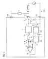
- FIG. 1 shows a detection circuit according to the proposed principle.
- the detection circuit comprises a measurement path which comprises a detection node OUT, a signal limiter 1, a filter 2 and a short-circuit detector 3.
- the detection node OUT is connected to a signal input 11 of the signal limiter 1.
- a signal output 12 of the signal limiter 1 is coupled to the filter 2.
- the filter 2 is designed as an RC element and comprises a resistor R1 and a capacitor C1.
- the resistor R1 is connected both to the signal output 12 and to a first detector input 31 of the short-circuit detector 3.
- the short-circuit detector 3 also has a second detector input 32, to which an adjustable threshold value Vshdet is applied.
- a detector output 33 is connected to a control path via a control input 41.
- the control path comprises a control circuit 4 for controlling a switch 5 which on the one hand has the control input 41 and on the other hand comprises a debouncer 401 and a switching device 402.
- the debouncer 401 is applied to the control input 41 and is coupled to the switching device 402.
- a control output 42 connects the switching device 402 to the switch 5.
- the switch 5 is in turn coupled to the detection node OUT and a supply node VSS.
- a load L is connected to the detection circuit via the detection node OUT and a voltage supply VHV.
- the connected load L represents, for example, a relay, a lamp or a switching input of a PLC control.
- an EMC generator EMC is coupled to the detection circuit via the detection node OUT and the supply voltage VSS.
- the detection circuit now detects signals present at the detection node and has means for distinguishing between signals as to whether they indicate a short circuit or not.
- the signals present at the detection node include sensor signals (or short-circuit signals) and EMC signals generated by the EMC generator EMC.
- the EMC generator in the normal use case, for example, a parallel laid cable or other electrical variables in the immediate vicinity of the circuit.
- the signal VEMC which is applied to the detection node OUT, the signal limiter 1 passed.
- the signal amplitude of the signal VEMC is symmetrically limited.
- the limitation takes place within a measuring interval, which is defined by a lower interval limit MIN and an upper interval limit MAX.
- An intermediate signal limited in this way is transferred from the signal limiter 1 to a filter 2.
- This is preferably a low-pass filter, consisting of the resistor R1 and the capacitor C1. In this way, a filtered intermediate signal is generated, which is present at the first detection input 31 in the sequence.
- the short-circuit detector 3 is for example as a Performed comparator, at the second input 32 of the adjustable threshold Vshdet is applied.
- the threshold value Vshdet is preferably selected such that it corresponds to the middle of the measurement interval MIN, MAX. In this way, it is ensured that the filtered intermediate signal Vdet generally remains below the threshold value Vshdet. Thus, no short-circuit detection event is triggered for different signal amplitudes of interference signals applied to the detection node OUT.
- the short-circuit detector indicates a short circuit, it generates a control signal, which is passed to the control path via the control input 41.
- the control circuit 4 controls the switch 5.
- time intervals t can be set on the optional debouncer 401.
- the control signal causes switch device 402 to switch switch 5 (eg, an NMOS transistor (NMOS) or other suitable transistors.)
- switch 5 is opened (eg, the NMOS transistor is turned off).
- the adjustable time interval t can be suitably programmed. In a sense, the debouncer 401 is thus an additional low-pass filter, but which is realized digitally.
- the measurement path allows increased accuracy of the short circuit detection.
- the short-circuit detection becomes independent of a signal amplitude of the voltage VEMC applied to the detection node OUT in a wide range. This is for example by a parasitic diode effect DPARA by the switch 5 strongly asymmetric.
- asymmetric signals at the detection node OUT can be considered with high accuracy. Furthermore, the accuracy of short-circuit detection by the low-pass filter 2 and comparison with the threshold value Vshdet is further improved.
- the optional debouncer 401 furthermore has the advantageous effect that, after the detection of a short circuit, the disconnection times of a connected load can be kept low.
- the switch 5 can, without limiting the invention as in FIG. 1 shown as a low-side, or alternatively designed as a high-side switch.
- the introduced principles of the detection circuit can be modified accordingly and applied to the respective switch type. Accordingly, depending on the type, the switch 5 can be operated by means of the power supply VHV or the supply voltage VSS.
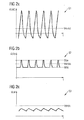
- FIGS. 2A, 2B and 2C show the waveforms to those in the FIG. 1 marked positions S1, S2 and S3.
- the occurring signal VEMC, Vclip, Vdet is plotted against the time t.
- the FIG. 1 is this point denoted by S1.
- the applied signal VEMC shows a strongly asymmetric signal waveform. However, this can also be triggered by the source of the interfering signal VEMC itself.
- the signal VEMC is on average above the threshold value Vshdet and would indicate a short circuit to the short-circuit detector 3 without further measures.
- FIG. 2B shows the waveform at the point S2 of FIG. 1 and indicates the limited intermediate signal Vclip after the signal amplitude of the signal VEMC has been limited by the signal limiter 1. Due to the symmetrical measuring interval MIN, MAX, this signal amplitude of the limited intermediate signal Vclip is correspondingly limited and is, on average, at the threshold value Vshdet or below.
- Figure 2C shows the filtered intermediate signal Vdet plotted against time T at location S3 of FIG. 1 .
- Filtering ensures that interference signals remain below the threshold value Vshdet as a result of EMC conditions, even with very different and also asymmetrical signal amplitudes. These can then be clearly distinguished from short circuit detection signals.
- Such a short-circuit signal would, for example, be above the threshold value Vshdet and also hardly fluctuate in time as long as the short-circuit exists.
Landscapes
- Physics & Mathematics (AREA)
- General Physics & Mathematics (AREA)
- Electronic Switches (AREA)
- Measurement Of Current Or Voltage (AREA)
- Emergency Protection Circuit Devices (AREA)
- Protection Of Static Devices (AREA)
- Networks Using Active Elements (AREA)
Claims (8)
- Circuit de détection comportant- une voie de détection, comprenant:- un limiteur de signal (1) destiné à limiter l'amplitude d'un signal à un intervalle de mesure (MIN, MAX), lequel est réglable moyennant une valeur seuil, la valeur seuil déterminant le milieu de l'intervalle de mesure (MIN, MAX) et le limiteur de signal (1) étant relié à un noeud de détection (OUT) moyennant une entrée de signal (11),- un filtre (2) qui est couplé à une sortie de signal (12) du limiteur de signal (1), et- un détecteur de court-circuit (3) pourvu d'une première et d'une deuxième entrée de détecteur (31, 32), ainsi que d'une sortie de détecteur (33), la première entrée de détecteur (31) étant couplée au filtre (2), et comportant- une voie de commande, comprenant:- un circuit de commutation de contrôle (4) destiné à commander un commutateur (5), et qui est couplé à la sortie de détecteur (33) moyennant une entrée de contrôle (41) et relié au commutateur (5) moyennant une sortie de contrôle (42), et- le commutateur (5), qui est couplé au noeud de détection (OUT) et à un noeud d'alimentation (VSS).
- Circuit de détection selon la revendication 1, dans lequel le filtre (2) est exécuté comme filtre passe-bas.
- Circuit de détection selon la revendication 1 ou 2, dans lequel le détecteur de court-circuit (3)- est exécuté comme comparateur, et- la valeur seuil réglable (Vshdet) peut être amenée au niveau de la deuxième entrée de détecteur (32).
- Circuit de détection selon l'une des revendications 1 à 3, dans lequel- le circuit de commutation de contrôle (4) comporte un dispositif anti-rebond (401) qui est relié à l'entrée de contrôle (41) et au filtre (2), et- le dispositif anti-rebond (401) est configuré pour commander le commutateur (5) à intervalles de temps réglables.
- Circuit de détection selon l'une des revendications 1 à 4, dans lequel le commutateur (5) comporte un transistor- dont le côté charge relie le noeud de détection (OUT) et le noeud d'alimentation (VSS) pour une tension d'alimentation, et- dont le côté commande est relié à la sortie de contrôle (42).
- Circuit de détection selon l'une des revendications 1 à 5, dans lequel le commutateur (5) comprend un transistor bipolaire ou unipolaire ou d'autres éléments semiconducteurs commutables.
- Procédé pour faire fonctionner un circuit de détection, comportant:- l'acquisition d'un signal (EMC) au niveau d'un noeud de détection (OUT),- la limitation de l'amplitude du signal (EMC) à un intervalle de mesure (MIN, MAX), lequel est réglable moyennant une valeur seuil qui détermine le milieu de l'intervalle de mesure (MIN, MAX),- le filtrage d'un signal intermédiaire (Vclip) reçu suite à la limitation de l'amplitude de signal,- la détection d'un court-circuit en fonction d'une comparaison du signal intermédiaire filtré (Vdet) avec un signal de comparaison (Vshdet) déterminé précédemment, lequel est déterminé par la valeur seuil réglable, et- l'application d'un potentiel de référence (VSS) au niveau du noeud de détection (OUT) en fonction de la détection du court-circuit.
- Procédé selon la revendication 7, dans lequel la détection du court-circuit se répète à intervalles de temps réglables.
Applications Claiming Priority (2)
| Application Number | Priority Date | Filing Date | Title |
|---|---|---|---|
| DE102010013322A DE102010013322B4 (de) | 2010-03-30 | 2010-03-30 | Detektionsschaltung und Verfahren zum Betreiben einer Detektionsschaltung |
| PCT/EP2011/053197 WO2011120756A1 (fr) | 2010-03-30 | 2011-03-03 | Circuit de détection et procédé pour faire fonctionner un circuit de détection |
Publications (2)
| Publication Number | Publication Date |
|---|---|
| EP2553811A1 EP2553811A1 (fr) | 2013-02-06 |
| EP2553811B1 true EP2553811B1 (fr) | 2014-01-22 |
Family
ID=44148776
Family Applications (1)
| Application Number | Title | Priority Date | Filing Date |
|---|---|---|---|
| EP11707645.5A Not-in-force EP2553811B1 (fr) | 2010-03-30 | 2011-03-03 | Circuit de détection et procédé pour faire fonctionner un circuit de détection |
Country Status (5)
| Country | Link |
|---|---|
| US (1) | US9519012B2 (fr) |
| EP (1) | EP2553811B1 (fr) |
| JP (1) | JP5537729B2 (fr) |
| DE (1) | DE102010013322B4 (fr) |
| WO (1) | WO2011120756A1 (fr) |
Families Citing this family (5)
| Publication number | Priority date | Publication date | Assignee | Title |
|---|---|---|---|---|
| US20130314836A1 (en) * | 2012-05-24 | 2013-11-28 | Allegro Microsystems, Inc. | Transistor Overcurrent Detection |
| CN104750089B (zh) * | 2013-12-25 | 2017-11-14 | 珠海格力电器股份有限公司 | 传感器信号的检测方法及装置 |
| DE102015222990A1 (de) | 2015-11-20 | 2017-05-24 | Zf Friedrichshafen Ag | Sichere Steuerung eines Verbrauchers |
| CN109116175A (zh) * | 2018-10-16 | 2019-01-01 | 浙江强泰能源科技有限公司 | 一种火灾监控装置电路 |
| JP2023154379A (ja) | 2022-04-06 | 2023-10-19 | 東洋インキScホールディングス株式会社 | 記録液セット、印刷物の製造方法、及び、印刷物 |
Family Cites Families (13)
| Publication number | Priority date | Publication date | Assignee | Title |
|---|---|---|---|---|
| CA2172890C (fr) | 1995-06-06 | 2005-02-22 | Harold R. Schnetzka | Circuit de commande d'interrupteur |
| DE19605023C2 (de) * | 1996-01-31 | 1999-08-05 | Siemens Ag | Verfahren zum Erfassen einer sprunghaften Änderung einer elektrischen Wechselgröße |
| IT1305598B1 (it) * | 1996-12-10 | 2001-05-09 | Abb Research Ltd | Metodo per il risconoscimento di condizioni di corto circuito edispositivo che utilizza tale metodo |
| US7542866B1 (en) * | 1999-01-21 | 2009-06-02 | Rosemount Inc. | Threshold setting for a radar level transmitter |
| JP3767445B2 (ja) * | 2001-09-28 | 2006-04-19 | アンデン株式会社 | 過電流保護機能を有する電源供給装置、負荷駆動装置および車両用電源供給装置 |
| US7592776B2 (en) * | 2001-11-07 | 2009-09-22 | Quallion Llc | Energy storage device configured to discharge energy in response to unsafe conditions |
| JP2005341663A (ja) * | 2004-05-25 | 2005-12-08 | Yazaki Corp | 過電流検出装置 |
| US9769090B2 (en) * | 2005-01-25 | 2017-09-19 | Linear Technology Corporation | Adjusting current limit thresholds based on power requirement of powered device in system for providing power over communication link |
| JP4701767B2 (ja) * | 2005-03-18 | 2011-06-15 | トヨタ自動車株式会社 | 電源装置 |
| US7489483B2 (en) * | 2006-09-19 | 2009-02-10 | Flextronics Automotive Inc. | System and method for look ahead detection of electrical problems at a motor of a vehicle |
| US7532010B2 (en) * | 2006-09-25 | 2009-05-12 | Delphi Technologies, Inc. | Sensing circuit and method for diagnosing open and short circuit conditions of a sensor |
| US20080212246A1 (en) * | 2006-12-31 | 2008-09-04 | Texas Instruments Incorporated | Systems and Methods for Detecting Shorts in Electrical Distribution Systems |
| US8005632B2 (en) * | 2007-11-07 | 2011-08-23 | GM Global Technology Operations LLC | Method and apparatus for detecting faults in a current sensing device |
-
2010
- 2010-03-30 DE DE102010013322A patent/DE102010013322B4/de not_active Expired - Fee Related
-
2011
- 2011-03-03 US US13/637,360 patent/US9519012B2/en active Active
- 2011-03-03 WO PCT/EP2011/053197 patent/WO2011120756A1/fr active Application Filing
- 2011-03-03 EP EP11707645.5A patent/EP2553811B1/fr not_active Not-in-force
- 2011-03-03 JP JP2013501710A patent/JP5537729B2/ja not_active Expired - Fee Related
Also Published As
| Publication number | Publication date |
|---|---|
| US20130076369A1 (en) | 2013-03-28 |
| US9519012B2 (en) | 2016-12-13 |
| JP2013528040A (ja) | 2013-07-04 |
| DE102010013322A1 (de) | 2011-10-06 |
| EP2553811A1 (fr) | 2013-02-06 |
| WO2011120756A1 (fr) | 2011-10-06 |
| JP5537729B2 (ja) | 2014-07-02 |
| DE102010013322B4 (de) | 2011-11-17 |
Similar Documents
| Publication | Publication Date | Title |
|---|---|---|
| DE102016100498B4 (de) | Leistungsschaltvorrichtung | |
| EP2519960B1 (fr) | Dispositif de contrôle de circuit électrique, dispositif de commutation pour l'alimentation d'un récepteur et procédé de fonctionnement d'un dispositif de commutation | |
| EP2068158B1 (fr) | Appareil de mesure de courant de charge | |
| EP2553811B1 (fr) | Circuit de détection et procédé pour faire fonctionner un circuit de détection | |
| DE102007056956A1 (de) | Schaltung zur Regelung der Stromversorgung eines Verbrauchers und Verfahren zum Betrieb einer Schaltung | |
| DE102014202460B3 (de) | Verfahren zum Erkennen eines Leitungskurzschlusses oder einer Leitungsunterbrechung bei einer geschalteten induktiven Last | |
| DE102014219882A1 (de) | Stromversorgungseinrichtung | |
| DE112015000270T5 (de) | Halbleitervorrichtung | |
| DE102008051074B4 (de) | Verfahren und Vorrichtung zum Überwachen einer durch einen Leistungshalbleiterschalter angesteuerten Last | |
| DE102015222990A1 (de) | Sichere Steuerung eines Verbrauchers | |
| DE102012111070B4 (de) | Sicherheitsbezogene Vorrichtung zum sicheren Schalten einer elektrischen Last | |
| DE19705339C2 (de) | Smart-Schalter sowie Verfahren zur Open-Load-Diagnose derselben | |
| DE102022106935B3 (de) | Intelligenter halbleiterschalter | |
| EP2876509B1 (fr) | Commande de sécurité | |
| DE102017108769B4 (de) | Steuereinrichtung für einen Leistungshalbleiterschalter | |
| DE102020124902A1 (de) | Ansteuerung einer Haltebremse | |
| WO2021213728A1 (fr) | Dispositif de commutation et procédé pour actionner un commutateur à semi-conducteur | |
| DE102008029680A1 (de) | Verfahren und elektronische Schaltung für eine elektronische Schaltungseinheit | |
| DE202015103339U1 (de) | Schaltungsanordnung für einen sicheren digitalen Schaltausgang | |
| DE102005046993B3 (de) | Vorrichtung und Verfahren zum Erzeugen eines Leistungssignals aus einem Laststrom | |
| EP2799946B1 (fr) | Procédé de réalisation d'une compatibilité entre d'un appareil de terrain et un dispositif de diagnostique et dispositif d'interface | |
| EP2827217A1 (fr) | Limiteur de tension electrique et emploie d' un limiteur electrique pour determiner des mesure d' un element de puissance electrique | |
| DE102013223141A1 (de) | Elektronische Schaltungsanordnung | |
| DE4120478C2 (de) | Steuerschaltung für einen Feldeffekttransistor | |
| DE102008029679B4 (de) | System, Verfahren und elektronische Schaltung für mindestens eine elektronische Schaltungseinheit |
Legal Events
| Date | Code | Title | Description |
|---|---|---|---|
| PUAI | Public reference made under article 153(3) epc to a published international application that has entered the european phase |
Free format text: ORIGINAL CODE: 0009012 |
|
| 17P | Request for examination filed |
Effective date: 20120906 |
|
| AK | Designated contracting states |
Kind code of ref document: A1 Designated state(s): AL AT BE BG CH CY CZ DE DK EE ES FI FR GB GR HR HU IE IS IT LI LT LU LV MC MK MT NL NO PL PT RO RS SE SI SK SM TR |
|
| DAX | Request for extension of the european patent (deleted) | ||
| GRAP | Despatch of communication of intention to grant a patent |
Free format text: ORIGINAL CODE: EPIDOSNIGR1 |
|
| INTG | Intention to grant announced |
Effective date: 20130904 |
|
| GRAS | Grant fee paid |
Free format text: ORIGINAL CODE: EPIDOSNIGR3 |
|
| GRAA | (expected) grant |
Free format text: ORIGINAL CODE: 0009210 |
|
| AK | Designated contracting states |
Kind code of ref document: B1 Designated state(s): AL AT BE BG CH CY CZ DE DK EE ES FI FR GB GR HR HU IE IS IT LI LT LU LV MC MK MT NL NO PL PT RO RS SE SI SK SM TR |
|
| REG | Reference to a national code |
Ref country code: GB Ref legal event code: FG4D Free format text: NOT ENGLISH |
|
| REG | Reference to a national code |
Ref country code: CH Ref legal event code: EP |
|
| REG | Reference to a national code |
Ref country code: AT Ref legal event code: REF Ref document number: 651182 Country of ref document: AT Kind code of ref document: T Effective date: 20140215 |
|
| REG | Reference to a national code |
Ref country code: IE Ref legal event code: FG4D Free format text: LANGUAGE OF EP DOCUMENT: GERMAN |
|
| REG | Reference to a national code |
Ref country code: DE Ref legal event code: R096 Ref document number: 502011002098 Country of ref document: DE Effective date: 20140306 |
|
| REG | Reference to a national code |
Ref country code: NL Ref legal event code: VDEP Effective date: 20140122 |
|
| REG | Reference to a national code |
Ref country code: LT Ref legal event code: MG4D |
|
| PG25 | Lapsed in a contracting state [announced via postgrant information from national office to epo] |
Ref country code: IS Free format text: LAPSE BECAUSE OF FAILURE TO SUBMIT A TRANSLATION OF THE DESCRIPTION OR TO PAY THE FEE WITHIN THE PRESCRIBED TIME-LIMIT Effective date: 20140522 Ref country code: LT Free format text: LAPSE BECAUSE OF FAILURE TO SUBMIT A TRANSLATION OF THE DESCRIPTION OR TO PAY THE FEE WITHIN THE PRESCRIBED TIME-LIMIT Effective date: 20140122 Ref country code: NO Free format text: LAPSE BECAUSE OF FAILURE TO SUBMIT A TRANSLATION OF THE DESCRIPTION OR TO PAY THE FEE WITHIN THE PRESCRIBED TIME-LIMIT Effective date: 20140422 |
|
| PG25 | Lapsed in a contracting state [announced via postgrant information from national office to epo] |
Ref country code: SE Free format text: LAPSE BECAUSE OF FAILURE TO SUBMIT A TRANSLATION OF THE DESCRIPTION OR TO PAY THE FEE WITHIN THE PRESCRIBED TIME-LIMIT Effective date: 20140122 Ref country code: NL Free format text: LAPSE BECAUSE OF FAILURE TO SUBMIT A TRANSLATION OF THE DESCRIPTION OR TO PAY THE FEE WITHIN THE PRESCRIBED TIME-LIMIT Effective date: 20140122 Ref country code: FI Free format text: LAPSE BECAUSE OF FAILURE TO SUBMIT A TRANSLATION OF THE DESCRIPTION OR TO PAY THE FEE WITHIN THE PRESCRIBED TIME-LIMIT Effective date: 20140122 Ref country code: ES Free format text: LAPSE BECAUSE OF FAILURE TO SUBMIT A TRANSLATION OF THE DESCRIPTION OR TO PAY THE FEE WITHIN THE PRESCRIBED TIME-LIMIT Effective date: 20140122 Ref country code: CY Free format text: LAPSE BECAUSE OF FAILURE TO SUBMIT A TRANSLATION OF THE DESCRIPTION OR TO PAY THE FEE WITHIN THE PRESCRIBED TIME-LIMIT Effective date: 20140122 Ref country code: PT Free format text: LAPSE BECAUSE OF FAILURE TO SUBMIT A TRANSLATION OF THE DESCRIPTION OR TO PAY THE FEE WITHIN THE PRESCRIBED TIME-LIMIT Effective date: 20140522 |
|
| PG25 | Lapsed in a contracting state [announced via postgrant information from national office to epo] |
Ref country code: HR Free format text: LAPSE BECAUSE OF FAILURE TO SUBMIT A TRANSLATION OF THE DESCRIPTION OR TO PAY THE FEE WITHIN THE PRESCRIBED TIME-LIMIT Effective date: 20140122 Ref country code: LV Free format text: LAPSE BECAUSE OF FAILURE TO SUBMIT A TRANSLATION OF THE DESCRIPTION OR TO PAY THE FEE WITHIN THE PRESCRIBED TIME-LIMIT Effective date: 20140122 Ref country code: RS Free format text: LAPSE BECAUSE OF FAILURE TO SUBMIT A TRANSLATION OF THE DESCRIPTION OR TO PAY THE FEE WITHIN THE PRESCRIBED TIME-LIMIT Effective date: 20140122 |
|
| REG | Reference to a national code |
Ref country code: DE Ref legal event code: R097 Ref document number: 502011002098 Country of ref document: DE |
|
| PG25 | Lapsed in a contracting state [announced via postgrant information from national office to epo] |
Ref country code: CZ Free format text: LAPSE BECAUSE OF FAILURE TO SUBMIT A TRANSLATION OF THE DESCRIPTION OR TO PAY THE FEE WITHIN THE PRESCRIBED TIME-LIMIT Effective date: 20140122 Ref country code: DK Free format text: LAPSE BECAUSE OF FAILURE TO SUBMIT A TRANSLATION OF THE DESCRIPTION OR TO PAY THE FEE WITHIN THE PRESCRIBED TIME-LIMIT Effective date: 20140122 Ref country code: RO Free format text: LAPSE BECAUSE OF FAILURE TO SUBMIT A TRANSLATION OF THE DESCRIPTION OR TO PAY THE FEE WITHIN THE PRESCRIBED TIME-LIMIT Effective date: 20140122 Ref country code: EE Free format text: LAPSE BECAUSE OF FAILURE TO SUBMIT A TRANSLATION OF THE DESCRIPTION OR TO PAY THE FEE WITHIN THE PRESCRIBED TIME-LIMIT Effective date: 20140122 Ref country code: LU Free format text: LAPSE BECAUSE OF FAILURE TO SUBMIT A TRANSLATION OF THE DESCRIPTION OR TO PAY THE FEE WITHIN THE PRESCRIBED TIME-LIMIT Effective date: 20140303 |
|
| REG | Reference to a national code |
Ref country code: CH Ref legal event code: PL |
|
| PG25 | Lapsed in a contracting state [announced via postgrant information from national office to epo] |
Ref country code: SK Free format text: LAPSE BECAUSE OF FAILURE TO SUBMIT A TRANSLATION OF THE DESCRIPTION OR TO PAY THE FEE WITHIN THE PRESCRIBED TIME-LIMIT Effective date: 20140122 Ref country code: PL Free format text: LAPSE BECAUSE OF FAILURE TO SUBMIT A TRANSLATION OF THE DESCRIPTION OR TO PAY THE FEE WITHIN THE PRESCRIBED TIME-LIMIT Effective date: 20140122 |
|
| PLBE | No opposition filed within time limit |
Free format text: ORIGINAL CODE: 0009261 |
|
| STAA | Information on the status of an ep patent application or granted ep patent |
Free format text: STATUS: NO OPPOSITION FILED WITHIN TIME LIMIT |
|
| REG | Reference to a national code |
Ref country code: FR Ref legal event code: ST Effective date: 20141128 |
|
| 26N | No opposition filed |
Effective date: 20141023 |
|
| REG | Reference to a national code |
Ref country code: IE Ref legal event code: MM4A |
|
| PG25 | Lapsed in a contracting state [announced via postgrant information from national office to epo] |
Ref country code: LI Free format text: LAPSE BECAUSE OF NON-PAYMENT OF DUE FEES Effective date: 20140331 Ref country code: CH Free format text: LAPSE BECAUSE OF NON-PAYMENT OF DUE FEES Effective date: 20140331 Ref country code: IE Free format text: LAPSE BECAUSE OF NON-PAYMENT OF DUE FEES Effective date: 20140303 Ref country code: FR Free format text: LAPSE BECAUSE OF NON-PAYMENT OF DUE FEES Effective date: 20140331 |
|
| REG | Reference to a national code |
Ref country code: DE Ref legal event code: R097 Ref document number: 502011002098 Country of ref document: DE Effective date: 20141023 |
|
| PG25 | Lapsed in a contracting state [announced via postgrant information from national office to epo] |
Ref country code: SI Free format text: LAPSE BECAUSE OF FAILURE TO SUBMIT A TRANSLATION OF THE DESCRIPTION OR TO PAY THE FEE WITHIN THE PRESCRIBED TIME-LIMIT Effective date: 20140122 |
|
| GBPC | Gb: european patent ceased through non-payment of renewal fee |
Effective date: 20150303 |
|
| PG25 | Lapsed in a contracting state [announced via postgrant information from national office to epo] |
Ref country code: GB Free format text: LAPSE BECAUSE OF NON-PAYMENT OF DUE FEES Effective date: 20150303 |
|
| PG25 | Lapsed in a contracting state [announced via postgrant information from national office to epo] |
Ref country code: MT Free format text: LAPSE BECAUSE OF FAILURE TO SUBMIT A TRANSLATION OF THE DESCRIPTION OR TO PAY THE FEE WITHIN THE PRESCRIBED TIME-LIMIT Effective date: 20140122 |
|
| PG25 | Lapsed in a contracting state [announced via postgrant information from national office to epo] |
Ref country code: SM Free format text: LAPSE BECAUSE OF FAILURE TO SUBMIT A TRANSLATION OF THE DESCRIPTION OR TO PAY THE FEE WITHIN THE PRESCRIBED TIME-LIMIT Effective date: 20140122 |
|
| PG25 | Lapsed in a contracting state [announced via postgrant information from national office to epo] |
Ref country code: MC Free format text: LAPSE BECAUSE OF FAILURE TO SUBMIT A TRANSLATION OF THE DESCRIPTION OR TO PAY THE FEE WITHIN THE PRESCRIBED TIME-LIMIT Effective date: 20140122 |
|
| PG25 | Lapsed in a contracting state [announced via postgrant information from national office to epo] |
Ref country code: GR Free format text: LAPSE BECAUSE OF FAILURE TO SUBMIT A TRANSLATION OF THE DESCRIPTION OR TO PAY THE FEE WITHIN THE PRESCRIBED TIME-LIMIT Effective date: 20140423 Ref country code: BG Free format text: LAPSE BECAUSE OF FAILURE TO SUBMIT A TRANSLATION OF THE DESCRIPTION OR TO PAY THE FEE WITHIN THE PRESCRIBED TIME-LIMIT Effective date: 20140122 Ref country code: IT Free format text: LAPSE BECAUSE OF FAILURE TO SUBMIT A TRANSLATION OF THE DESCRIPTION OR TO PAY THE FEE WITHIN THE PRESCRIBED TIME-LIMIT Effective date: 20140122 |
|
| PG25 | Lapsed in a contracting state [announced via postgrant information from national office to epo] |
Ref country code: TR Free format text: LAPSE BECAUSE OF FAILURE TO SUBMIT A TRANSLATION OF THE DESCRIPTION OR TO PAY THE FEE WITHIN THE PRESCRIBED TIME-LIMIT Effective date: 20140122 Ref country code: BE Free format text: LAPSE BECAUSE OF FAILURE TO SUBMIT A TRANSLATION OF THE DESCRIPTION OR TO PAY THE FEE WITHIN THE PRESCRIBED TIME-LIMIT Effective date: 20140331 Ref country code: HU Free format text: LAPSE BECAUSE OF FAILURE TO SUBMIT A TRANSLATION OF THE DESCRIPTION OR TO PAY THE FEE WITHIN THE PRESCRIBED TIME-LIMIT; INVALID AB INITIO Effective date: 20110303 |
|
| REG | Reference to a national code |
Ref country code: AT Ref legal event code: MM01 Ref document number: 651182 Country of ref document: AT Kind code of ref document: T Effective date: 20160303 |
|
| PG25 | Lapsed in a contracting state [announced via postgrant information from national office to epo] |
Ref country code: AT Free format text: LAPSE BECAUSE OF NON-PAYMENT OF DUE FEES Effective date: 20160303 |
|
| PG25 | Lapsed in a contracting state [announced via postgrant information from national office to epo] |
Ref country code: MK Free format text: LAPSE BECAUSE OF FAILURE TO SUBMIT A TRANSLATION OF THE DESCRIPTION OR TO PAY THE FEE WITHIN THE PRESCRIBED TIME-LIMIT Effective date: 20140122 |
|
| PG25 | Lapsed in a contracting state [announced via postgrant information from national office to epo] |
Ref country code: AL Free format text: LAPSE BECAUSE OF FAILURE TO SUBMIT A TRANSLATION OF THE DESCRIPTION OR TO PAY THE FEE WITHIN THE PRESCRIBED TIME-LIMIT Effective date: 20140122 |
|
| PGFP | Annual fee paid to national office [announced via postgrant information from national office to epo] |
Ref country code: DE Payment date: 20220322 Year of fee payment: 12 |
|
| P01 | Opt-out of the competence of the unified patent court (upc) registered |
Effective date: 20230822 |
|
| REG | Reference to a national code |
Ref country code: DE Ref legal event code: R119 Ref document number: 502011002098 Country of ref document: DE |
|
| PG25 | Lapsed in a contracting state [announced via postgrant information from national office to epo] |
Ref country code: DE Free format text: LAPSE BECAUSE OF NON-PAYMENT OF DUE FEES Effective date: 20231003 |