EP2549536A1 - Halbleiterstruktur zur Photonendetektion - Google Patents
Halbleiterstruktur zur Photonendetektion Download PDFInfo
- Publication number
- EP2549536A1 EP2549536A1 EP11006012A EP11006012A EP2549536A1 EP 2549536 A1 EP2549536 A1 EP 2549536A1 EP 11006012 A EP11006012 A EP 11006012A EP 11006012 A EP11006012 A EP 11006012A EP 2549536 A1 EP2549536 A1 EP 2549536A1
- Authority
- EP
- European Patent Office
- Prior art keywords
- substrate
- semiconductor structure
- contact region
- structure according
- doped
- Prior art date
- Legal status (The legal status is an assumption and is not a legal conclusion. Google has not performed a legal analysis and makes no representation as to the accuracy of the status listed.)
- Granted
Links
Images


Classifications
-
- H—ELECTRICITY
- H10—SEMICONDUCTOR DEVICES; ELECTRIC SOLID-STATE DEVICES NOT OTHERWISE PROVIDED FOR
- H10F—INORGANIC SEMICONDUCTOR DEVICES SENSITIVE TO INFRARED RADIATION, LIGHT, ELECTROMAGNETIC RADIATION OF SHORTER WAVELENGTH OR CORPUSCULAR RADIATION
- H10F99/00—Subject matter not provided for in other groups of this subclass
-
- H—ELECTRICITY
- H10—SEMICONDUCTOR DEVICES; ELECTRIC SOLID-STATE DEVICES NOT OTHERWISE PROVIDED FOR
- H10F—INORGANIC SEMICONDUCTOR DEVICES SENSITIVE TO INFRARED RADIATION, LIGHT, ELECTROMAGNETIC RADIATION OF SHORTER WAVELENGTH OR CORPUSCULAR RADIATION
- H10F39/00—Integrated devices, or assemblies of multiple devices, comprising at least one element covered by group H10F30/00, e.g. radiation detectors comprising photodiode arrays
- H10F39/80—Constructional details of image sensors
- H10F39/807—Pixel isolation structures
Definitions
- the invention relates to a semiconductor structure for photon detection according to the preamble of claim 1.
- the object of the invention is to provide a semiconductor structure for photon detection, which enables cost savings in production.
- a semiconductor structure for photon detection comprising: a substrate made of a semiconductor material with a first doping, a contact region, which is attached to the front side of the substrate, a bias layer of one Semiconductor material having a second doping, which is arranged on the back side of the substrate spaced from the contact region, wherein the contact region at least partially opposite to the bias layer, so that in the lateral direction an overlap region is present, a guard ring, which is arranged on the front side of the substrate and surrounds the contact region, wherein between the contact region and the guard ring, a reverse voltage can be applied, characterized in that the overlap region has a lateral extent which is at least a quarter of the distance between the contact region and the bias layer.
- the guard ring is a kind of protective structure, which can shield the contact area from its surroundings or from further semiconductor structures by the potential applied to it. Among other things, in particular also vagabond charge carriers can be intercepted; it is also possible to lower the parasitic resistances.
- the guard ring allows a depletion to take place laterally of the guard ring, i. a depletion zone can be formed so that the contact area is shielded from other areas such as possibly CMOS structures or sensor structures.
- the distance between the contact region and the bias layer may correspond to the thickness of the substrate.
- the bias layer is accordingly formed on the back side of the substrate.
- the overlap area in the sense of the invention is the area in which the contact area extends laterally over the bias layer.
- the semiconductor structure may preferably be used as a photodetector.
- it can be used as a photodetector for serve the infrared range.
- the bias layer on the back surface may serve to deplete a zone of depletion between areas on the front side with a first type dopant (substrate contact) and the bias layer. If an electron-hole pair is produced by the absorption of a photon in this depletion zone, these are separated due to the electric field in the depletion zone. In particular, the electrons can be detected in the substrate contact on the Verdeseite of the substrate.
- a cost saving can be achieved by the semiconductor structure according to the invention in that the bias layer on the back does not have to be specifically contacted.
- this layer on the back which may be formed in commercial semiconductor structures, in particular made of metal, a wire bonded or contacting by the silicon material (English: throughsilicon via, abbr .: TSV) produced.
- TSV throughsilicon via, abbr .: TSV
- this production can lead to high costs.
- such contacting can be avoided in the semiconductor structure according to the invention. Due to the measure that the minimum lateral extent through which the overlap region is formed is greater than a quarter of the substrate thickness or the distance between the contact region and the bias layer on the back, an influence of the bias layer can take place.
- a semiconductor material is regularly used for the corresponding substrate (for example germanium or silicon), while in different areas the doping in the manufacturing process can be different, such as a stronger or weaker doping and a doping of the same name or the same name.
- Another fundamental advantage of the semiconductor structure according to the invention is that in the Semiconductor manufacturing, such as in a process line machining the back can be reduced.
- a further advantage of the semiconductor structure for photon detection according to the invention is that it is possible to work with reduced voltages in order to be able to obtain a corresponding, sufficient depletion zone for detection.
- the contact region is designed such that the potential of the bias layer is influenced by the potential applied to it.
- the contact region itself is surrounded by and shielded by a guard ring, which is likewise arranged on the front side of the substrate.
- the reverse voltage itself is applied simultaneously between the contact area and the guard ring, that is, one pole of the corresponding voltage is applied to the contact area, the other on the guard ring.
- the polarity of the voltage depends on which doping the substrate or the remaining semiconductor material has. If the lateral extent was chosen to be less than one quarter of the thickness of the substrate, the potential in the region of the bulk material of the substrate between the contact region and the bias layer on the backside would be influenced essentially by the guard ring voltage.
- the potential becomes increasingly independent of the guard ring voltage as the lateral extent increases.
- the potential in the bulk material is affected by the potential applied to the contact region, but also the potential of the bias layer. The result is a potential channel, a conduit between the contact area and the opposing bias layer.
- the contact region may be formed by a metallic contact on the substrate surface. Furthermore, however, the contact region may also comprise a well formed in the substrate. This is accordingly unlike in comparison to the first doping, ie in comparison to the substrate doped. This also makes it possible for the contact region, which is designed as a trough, to extend deeper into the substrate and thus, for example, to influence the potential of the bias layer even more strongly.
- the substrate to dope weak in one embodiment of the invention, so it form high impedance.
- This material is particularly advantageous for photon detection, that is, for charge carrier separation in photon absorption.
- the doping of the second type is doped with different names compared to the doping of the first type.
- an influence on the bias layer is achieved by subtracting the majority charge carriers by the potential.
- the bias layer can be doped unlike in comparison to the substrate.
- the guard ring may have a doping of the same type in an embodiment of the invention as the substrate, i. H. the semiconductor material with doping of the first kind.
- the majority charge carriers of the guard ring are drawn off.
- the guard ring may be more heavily doped than the substrate. This stronger doping allows a special shielding function, which is intended to exercise the guard ring with respect to the contact area with respect to the other areas.
- the semiconductor structure is formed so that it can be illuminated from the back.
- this backlighting makes it possible for photons to penetrate into the region of the depletion zone in the most advantageous manner possible. It is also avoided to contact the back, or this with To equip other components, the light can penetrate into the substrate so unhindered, since no disturbing contacts, etc. on the way of the light in the way are. Among other things, the efficiency of the semiconductor structure in photon detection can thus be increased.
- At least one further region may be arranged which comprises at least one trough of a material doped with the same name as the contact region.
- at least one further region can be designed as a sensor component for the detection, in particular for the detection of photons. Since these regions are arranged laterally offset from the contact region, that is to say they are located on the front side of the semiconductor structure, they may not be in the way of backlighting, so that a higher photon yield can be achieved.
- an area can also be used as a depletion zone and thus for photon detection, which is laterally offset from the area below the contact area. Also, this part of the bulk material is thus used as an absorption area and becomes a depletion zone.
- the absorption region is in concern of the reverse voltage to the depletion zone.
- the substrate of the semiconductor structure is produced from silicon obtained in the zone-pulling process (English: float-zone silicon).
- This material is characterized by very low impurities and by particular homogeneity.
- the conductivity is several hundred ohms centimeters ( ⁇ cm) up to several k ⁇ cm.
- the semiconductor material with doping of the first type or the substrate in a development of the invention weakly n-doped.
- a correspondingly weak doping leads to a high resistance of the material and to a low density of majority charge carriers.
- a trench isolation (English: shallow-trench isolation, abbreviation: STI) is partially arranged between the contact region and the guard ring or the contact region and the at least one further region.
- a corresponding isolation leads to a further foreclosure with regard to the corresponding potential, if necessary.
- a particular advantage of the semiconductor structure according to the invention is to be able to achieve a particularly good quantum efficiency, in particular in the near infrared range.
- this is achieved by a so-called pin structure (abbreviation for: positive - intrinsic - negative).
- the extent of the depletion zone in the substrate is mainly influenced by the doping within the substrate. It should also be noted that the reverse voltage which can be applied to the front is limited and typically on the order of a few volts.
- Such photodetectors have the disadvantage that the absorption length can be substantially greater than the extent of the depletion zone. Accordingly, it may happen that a large number of generated charge carriers are formed during photon absorption outside the depletion zone in the bulk material. There, the minority carriers have only a short lifetime and are not exposed to any electric field, so that after splitting the charge carriers this can not be separated quickly enough and recombine again. Because of this Rekombins bulkes, which then arises when the corresponding electric field is not high enough to maintain a sufficient separation of the charge carriers or to allow a fast, the recombination counteracting withdrawal of charge carriers, a corresponding part of the split charge carriers will recombine and is lost for the detection.
- Another part of the generated charge carriers is subject to a lateral diffusion due to the missing electric field and is thus finally detected at a different location, namely not where corresponding photons that led to the separation of the charge carriers have actually been absorbed. blue).
- a corresponding diffusion process of the charge carriers generally proceeds comparatively slowly, so that the corresponding time correlation during detection can be lost because the corresponding charge carriers only diffuse away slowly and thus a corresponding time passes between the separation of the charge carriers and the actual detection.
- a corresponding electronics for detection can be applied on the front.
- These may be typical CMOS structures. It is particularly advantageous to shield these structures accordingly, in particular by means of a guard ring which surrounds the contact region. This guardring is also used to apply the blocking voltage.
- the corresponding shielding also provides a shielding of noise or additional effects by contacting the contact area with respect to any contacts of the other areas, such as the CMOS structures. A depletion zone can be created virtually throughout the bulk material become.
- a bias layer can be applied to the back side, which is doped differently with respect to the semiconductor material with doping of the first type, ie the semiconductor material of the substrate. If the semiconductor material with doping of the first type is, for example, weakly n-doped, then the bias layer is p-doped. This bias layer does not necessarily have to be contacted. However, in principle it is also conceivable to additionally provide, for example, a metal contact for this purpose, if appropriate also through the bulk material. However, this contacting can be avoided by the semiconductor structure according to the invention.
- conventional process lines for wafer production can be advantageously used, which allow a production of the front side (English: frontside processing), a thinning of the wafer (English: wafer thinning) and any processing of the back side (English: backside processing).
- the so-called "frontside processing" can be carried out in a commercially customary manner by producing dopants, for example by ion implantation, oxidation processes, metallization, STI, passivation, etc.
- resistors, transistors, etc. can be built up.
- active structures as well as so-called STI's different areas can be formed.
- the contact area in turn can be shielded from these areas with respect to its potential by a guard ring.
- the contact region may have a rectangular shape or be annular.
- the guard rings can be formed, for example, by deep-reaching implanted structures, for example by well structures.
- the substrate is formed of a lightly doped n-material, which was obtained, for example, in the zone pulling process.
- the guard rings are formed by n-doped wells.
- the area outside the area within the guard rings is at potential 0 (ground).
- a blocking voltage is applied, so that the guard ring is provided with a positive bias.
- the contact area is set to a negative potential. Due to the barrier, which is generated by the positive bias of the guard ring, there is virtually no leakage current between the two differently doped regions in the substrate.
- the substrate itself is only weakly doped, so that only a very small potential barrier with respect to the back pn junction survives. Accordingly, majority carriers of the bias layer, that is, holes, can flow to the negative terminal applied to the contact area. Accordingly, the negative bias of the contact region also affects the bias layer. It practically creates a "virtual" backside contact.
- this mode of action in the semiconductor material can also remain unchanged if charge carrier separation takes place by absorption of photons, that is, minority carriers are formed.
- the holes are more likely to flow towards the back as it is at a negative potential compared to the rest of the substrate. This, in turn, increases the potential at the backside of the semiconductor structure, from negative to zero, which in turn lowers the barrier with respect to the transition between the bias layer and the contact region. Finally, a dynamic equilibrium is established so that the backside remains at a substantially constant potential.
- a corresponding semiconductor structure according to the invention can also be used for applications in which time correlations are particularly important, that is, those applications in which the detection must be as close as possible to the photon absorption.
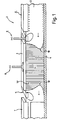
- FIG. 1 shows a schematic section through a semiconductor structure 1.
- This comprises a substrate 2, on which a contact region 3 is applied.
- a bias layer 4 On the back of the substrate there is a bias layer 4.
- a guard ring 5 is arranged around the contact 3.
- Lateral offset to the contact region 3 is a CCD sensor 6 and a further CMOS region 7.
- a reverse voltage is applied by the contact 3 is connected to the negative terminal 8, while the guard ring 5 is connected to the positive pole 9 ,
- the polarity with which the blocking voltage is ultimately applied depends inter alia on the doping of the semiconductor structures.
- the substrate 2 is weakly n-doped. It consists of silicon obtained by zone pulling.
- the guard ring in turn consists of an n-doped material which is doped more strongly than the substrate.
- the bias layer on the backside is p-doped.
- the potential applied to the contact region can influence the potential of the bias layer.
- the result is a kind of duct, the course is indicated by the contours 10.
- the holes which originate, for example, from the p-doped bias layer 4 or from the charge carrier elimination caused by photon absorption, move in the direction of the negative pole.
- the semiconductor structure is further designed such that the pn junction from the substrate to the bias layer has a relatively low barrier, so that the holes can also travel in the direction of the negative pole. Since the positive pole is applied to the n-doped guard ring, the majority charge carriers, the electrons are sucked from the positive pole.
- the guard ring in turn shields the contact region 3 from the CCD region 6 or the CMOS region 7. Now, when a photon in back irradiation in the photodetector 1, it can be absorbed in the depletion zone in the substrate 2 and split an electron-hole pair, the hole through the duct 10 'can be sucked and the electron for signal detection to Available.
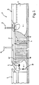
- FIG. 2 shows a similar representation similar to FIG. 1 with a kind of schematic equivalent circuit diagram, only for the understanding: The structure can be compared in a similar manner with a diode circuit 11 and with a transistor circuit 12.
- FIG. 3 shows a similar construction, in which the contact region 103, however, consists of a metallic contact 103a, which is applied to the substrate 102, as well as a highly doped p-well 103b and an underlying also heavily doped (p +) layer 103c.
- the substrate 102 is made of weakly n-doped, zoned pull-grown n-type material.
- the guard ring 105 in turn, a heavily n-doped layer 105a and an underlying further buried n-doped layer 105b include.
- the bias layer on the back side is heavily p-doped (reference numeral 104).
- a passivation 113 is applied, which serves to seal the surface. It is conceivable, for example, the use of a silicate glass for passivation.
- the negative pole 108 By applying the negative pole 108 at the contact region 103, the holes located there, the majority charge carriers of the p-well material, are drawn off. Analogous, namely the extraction of electrons is done by applying the positive pole 109 on the guard ring 105. Due to the wide lateral extent of the contact region 103 compared to the distance between the contact region 103 and the bias layer 104, a conduit 110 'is formed by the Lines 110 are indicated in each case. Furthermore, also located laterally offset from the contact region 103 is a CCD electronics 106 and further CMOS regions 107.
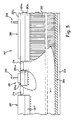
- FIGS. 4 to 6dar hire Another structure of a corresponding photodetector 201 is shown in FIGS FIGS. 4 to 6darched.
- This likewise includes a contact region 203 with a metallic contact 203a of a heavily doped p-well 203b underneath and a further p-doped layer 203c underneath.
- the actual substrate 202 in turn is weakly n-doped.
- the contact region 203 is surrounded by a guard ring 205.
- This comprises a metallic contact and a heavily n-doped well 205a and another n-doped layer 205b, which lies under the tub.
- a bias layer 204 which is heavily p-doped, is deposited on the backside, as well as a passivation layer 213.
- a corresponding CMOS structure 207 with an underlying, also shielding, p-doped layer 207 ' is also present.
- the guard ring is of a trench isolation 214 (English: shallow-trench isolation, STI).
- This STI structure serves to strengthen the demarcation of the individual areas.
- the contacting of the structure takes place in the usual way, that is, the negative pole 208 is applied to the contact region 203, while the positive pole 209 is applied to the guard ring 205.
- FIG. 6 only schematic replacement diagrams 215 and 216 are inserted for better explanation.
- the mutually connected diodes 215 illustrate accordingly the formation of a depletion zone.
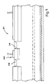
- FIGS. 7, 8 and 9 Examples are shown how contact regions 303, 403, 503 can be arranged and formed with respect to their shape.
- FIG. 7 shows a substrate 302 of a semiconductor structure in plan view with a front-mounted single and point-shaped contact area 303.
- FIG. 8 again shows a plurality of point-shaped contact areas 403 on a substrate 402.
- FIG. 9 shows an annular contact area 503 on a substrate 502.
- the semiconductor has a contact region on the front side of the substrate.
- a format of 50 microns x 200 microns comes into consideration.
- the contact region comprises a so-called p-source / drain implantation of one (p ++) - doped material (surface resistivity about 100 ⁇ or 100 ⁇ / sq., In the range of 0 nm to about 100 nm), in addition a p-well implantation with a (p +) - doped layer (specific sheet resistance: approx. 1000 ⁇ / sq., arranged in the range of approx. 0.1 ⁇ m to 1.0 ⁇ m depth).
- This p-well is designed so that a potential of -1 V to -5 V can be applied.
- a p-subimplantation is provided which consists of a (p +) -doped region (specific sheet resistance of approximately 1000 ⁇ / sq., Arranged at a depth of approximately 0.7 ⁇ m to 1.5 ⁇ m).
- the guard ring is also formed on the front side of the substrate and surrounds the contact area.
- the width of the guard ring is preferably about 10 microns, the distance to the contact area also about 10 microns.
- a trench isolation (STI) with a width of 10 ⁇ m is preferably provided inside and outside the guard ring.
- the guard ring accordingly comprises an n-source / drain implant of (n ++) doped material having a sheet resistivity of less than 100 ⁇ / sq. and a depth from the surface of 100 nm.
- the guard ring structure comprises an n-well implantation of (n +) - doped material (surface resistivity: about 800 ⁇ / sq., Depth about 0.7 microns to 1.5 ⁇ m, located in the range of 100 nm to 1000 nm depth).
- the n-well implantation is designed so that an isolation voltage of +5 V to +10 V can be applied.
- an n-buried layer implant (n-buried layer implant) formed as a buried n-layer is made of an (n +) -doped material (sheet resistivity: approx. 1300 ⁇ / sq., Provided, depth: approx. 0.5 ⁇ m to 1.0 ⁇ m), which is in the range of 500 nm to 700 nm depth).
- sheet resistivity approx. 1300 ⁇ / sq.
- depth approx. 0.5 ⁇ m to 1.0 ⁇ m
- a layer on the back side (English: backside layer) is provided, which is spaced from the contact area, but forms a lateral overlap with the contact area. It comprises a p-well implantation ((p +) - doped with a sheet resistivity of less than 1000 ⁇ / sq.), which reaches 200 nm deep from the back surface. On the surface, this layer (backside layer) is covered by an antireflective coating (ARC layer) of nitrides, ZbSiO or ZbSiNi).
- ARC layer antireflective coating
- the back layer is regularly formed homogeneously, ie without structuring and extends over the entire wafer range, if appropriate, apart from a narrow edge region, which is not thinned example and equipped on the back.
Landscapes
- Light Receiving Elements (AREA)
Abstract
Description
- Die Erfindung betrifft eine Halbleiterstruktur zur Photonendetektion nach dem Oberbegriff des Anspruchs 1.
- Aus dem Stand der Technik ist beispielsweise durch die
US 5, 786, 609 A ein Halbleiterdetektor bekannt, welcher eine Unipolarstruktur aufweist, sowie eine als Schicht an der Unterseite ausgebildete "Return-Elektrode", die zum Abzug der Leitungsträger aus der Verarmungszone ausgebildet ist. - Aufgabe der Erfindung ist es, eine Halbleiterstruktur zur Photonendetektion zur Verfügung zu stellen, welche eine Kostenersparnis bei der Produktion ermöglicht.
- Diese Aufgabe wird, ausgehend von einer Halbleiterstruktur der eingangs genannten Art, durch die kennzeichnenden Merkmale des Anspruchs 1 gelöst.
- Durch die in den abhängigen Ansprüchen genannten Maßnahmen sind vorteilhafte Weiterbildungen und Ausführungen der Erfindung möglich.
- Dementsprechend zeichnet sich eine erfindungsgemäße Halbleiterstruktur zur Photonendetektion, umfassend: ein Substrat aus einem Halbleitermaterial mit einer ersten Dotierung, einen Kontaktbereich, der an der Vorderseite des Substrates angebracht ist, eine Bias-Schicht aus einem Halbleitermaterial mit einer zweiten Dotierung, welche auf der Rückseite des Substrats beabstandet vom Kontaktbereich angeordnet ist, wobei der Kontaktbereich wenigstens teilweise der Bias-Schicht gegenüberliegt, so dass in lateraler Richtung ein Überlappbereich vorhanden ist, ein Guardring, der auf der Vorderseite des Substrats angeordnet ist und den Kontaktbereich umgibt, wobei zwischen dem Kontaktbereich und dem Guardring eine Sperrspannung anlegbar ist, dadurch aus, dass der Überlappbereich eine laterale Ausdehnung aufweist, die wenigstens ein Viertel der Distanz zwischen dem Kontaktbereich und der Bias-Schicht beträgt.
- Der Guardring ist eine Art Schutzstruktur, welche durch das an ihn angelegte Potential den Kontaktbereich von dessen Umgebung bzw. von weiteren Halbleiterstrukturen abschirmen kann. Unter anderem können insbesondere auch vagabundierende Ladungsträger abgefangen werden; es wird auch ermöglicht, die parasitären Widerstände zu senken.
- Bei der erfindungsgemäßen Halbleiterstrurktur ermöglicht der Guardring, dass seitlich des Guardrings eine Verarmung erfolgt, d.h. es kann eine Verarmungszone gebildet werden, sodass der Kontaktbereich von übrigen Bereichen wie gegebenenfalls CMOS-Strukturen bzw. Sensorstrukturen abgeschirmt ist.
- Wenn der Kontaktbereich beispielsweise lediglich dadurch gebildet wird, dass ein Metallkontakt auf das Substrat aufgebracht wird, kann die Distanz zwischen dem Kontaktbereich und der Bias-Schicht der Dicke des Substrates entsprechen.
- Die Bias-Schicht ist dementsprechend auf der Rückseite des Substrats ausgebildet. Der Überlappbereich im Sinne der Erfindung ist der Bereich, in dem der Kontaktbereich in lateraler Ausdehnung sich über der Bias-Schicht erstreckt.
- Die Halbleiterstruktur kann vorzugsweise als Photodetektor eingesetzt werden. Insbesondere kann sie als Photodetektor für den Infrarotbereich dienen. Die Bias-Schicht auf der Rückseite kann dazu dienen, zwischen Bereichen auf der Vorderseite mit einer Dotierung erster Art (Substratkontakt)und der Bias-Schicht eine Verarmungszone herzustellen (engl.: depletion zone). Wird durch die Absorption eines Photons in dieser Verarmungszone ein Elektron-Loch-Paar erzeugt, so werden diese aufgrund des elektrischen Feldes in der Verarmungszone getrennt. Insbesondere können die Elektronen im Substratkontakt auf der Verdeseite des Substrats nachgewiesen werden.
- Insbesondere kann durch die erfindungsgemäße Halbleiterstruktur eine Kostenersparnis dadurch erreicht werden, dass die Bias-Schicht auf der Rückseite nicht eigens kontaktiert werden muss. Üblicherweise wird für eine solche Kontaktierung dieser Schicht auf der Rückseite, die bei handelsüblichen Halbleiterstrukturen insbesondere aus Metall ausgebildet sein kann, ein Draht aufgebondet oder eine Kontaktierung durch das Siliziummaterial (engl.: throughsilicon via, Abk.: TSV) hergestellt. Diese Fertigung kann jedoch zu hohen Kosten führen. Eine derartige Kontaktierung kann jedoch bei der erfindungsgemäßen Halbleiterstruktur vermieden werden. Aufgrund der Maßnahme, dass die minimale Lateralausdehnung, durch welche der Überlappbereich gebildet wird, größer ist als ein Viertel der Substratdicke bzw. der Distanz zwischen dem Kontaktbereich und der Bias-Schicht auf der Rückseite beträgt, kann eine Beeinflussung der Bias-Schicht erfolgen.
- Grundsätzlich wird bei der Fertigung einer derartigen Halbleiterstruktur regelmäßig ein Halbleitermaterial für das entsprechende Substrat verwendet (z.B. Germanium oder Silizium), während in unterschiedlichen Bereichen die Dotierung beim Herstellungsprozess anders ausgebildet werden kann, etwa eine stärkere oder schwächere Dotierung sowie eine gleichnamige oder ungleichnamige Dotierung.
- Ein weiterer grundsätzlicher Vorteil der erfindungsgemäßen Halbleiterstruktur besteht darin, dass bei der Halbleiterfertigung, etwa in einer Prozessstraße die Bearbeitung der Rückseite reduziert werden kann. Ein weiterer Vorteil der erfindungsgemäßen Halbleiterstruktur zur Photonendetektion besteht darin, dass mit verringerten Spannungen gearbeitet werden kann, um eine entsprechende, ausreichende Verarmungszone zur Detektion erhalten zu können.
- Bei einer bevorzugten Weiterbildung der Erfindung ist der Kontaktbereich dazu ausgebildet, dass durch das an ihn angelegte Potential das Potential der Bias-Schicht beeinflusst wird. Der Kontaktbereich selbst wird durch einen Guardring, der ebenfalls auf der Vorderseite des Substrats angeordnet ist, umgeben und von diesem abgeschirmt. Die Sperrspannung selbst wird gleichzeitig zwischen dem Kontaktbereich und dem Guardring angelegt, das heißt, ein Pol der entsprechenden Spannung wird am Kontaktbereich angelegt, der andere am Guardring. Die Polung der Spannung hängt unter anderem davon ab, welche Dotierung das Substrat bzw. das übrige Halbleitermaterial aufweist. Würde die Lateralausdehnung kleiner als ein Viertel der Dicke des Substrats gewählt, so würde das Potential im Bereich des Bulkmaterials des Substrats zwischen dem Kontaktbereich und der Bias-Schicht auf der Rückseite im Wesentlichen durch die Guardring-Spannung beeinflusst. Dadurch allerdings, dass die Lateralausdehnung größer als ein Viertel der Dicke gewählt wird, also in die Größenordnung der Substratdicke gelangt, wird das Potential mit zunehmender Lateralausdehnung immer mehr unabhängig von der Guardring-Spannung. Schließlich wird nicht nur das Potential im Bulkmaterial durch das am Kontaktbereich angelegte Potential beeinflusst, sondern ebenfalls das Potential der Bias-Schicht. Es entsteht ein Potentialkanal, ein Leitungskanal zwischen dem Kontaktbereich und der gegenüberliegenden Bias-Schicht.
- Der Kontaktbereich kann durch eine metallische Kontaktierung auf der Substratoberfläche gebildet sein. Ferner kann der Kontaktbereich allerdings auch eine im Substrat ausgebildete Wanne umfassen. Diese wird dementsprechend ungleichnamig im Vergleich zur ersten Dotierung, also im Vergleich zum Substrat dotiert. Dadurch wird auch ermöglicht, dass der Kontaktbereich, der als Wanne ausgebildet ist, tiefer in das Substrat hineinreicht und somit zum Beispiel das Potential der Bias-Schicht noch stärker beeinflussen kann.
- Insbesondere ist es möglich, das Halbleitermaterial mit der Dotierung erster Art, d. h. insbesondere das Substrat, bei einer Ausführungsform der Erfindung schwach zu dotieren, es also hochohmig auszubilden. Dieses Material ist insbesondere vorteilhaft für die Photonendetektion, das heißt, für die Ladungsträgertrennung bei der Photonenabsorption.
- Ferner ist bei einer bevorzugten Weiterbildung der Erfindung die Dotierung zweiter Art im Vergleich zur Dotierung erster Art ungleichnamig dotiert. Durch Anlegen einer entsprechenden Sperrspannung wird eine Beeinflussung der Bias-Schicht dadurch erreicht, dass die Majoritätsladungsträger durch das Potential abgezogen werden. Somit erfolgt die Ausbildung einer Diode. Die Bias-Schicht kann dabei im Vergleich zum Substrat ungleichnamig dotiert sein.
- Der Guardring wiederum kann eine gleichnamige Dotierung bei einer Ausführungsform der Erfindung wie das Substrat, d. h. das Halbleitermaterial mit Dotierung erster Art, aufweisen. Durch die Kontaktierung mit der Sperrspannung werden wiederum die Majoritätsladungsträger des Guardrings abgezogen.
- Ferner kann bei einer Ausführungsform der Erfindung der Guardring stärker dotiert sein als das Substrat. Diese stärkere Dotierung ermöglicht eine besondere Abschirmungsfunktion, welche der Guardring hinsichtlich des Kontaktbereichs gegenüber den übrigen Bereichen ausüben soll.
- Bei einer bevorzugten Weiterbildung der Erfindung wird die Halbleiterstruktur so ausgebildet, dass sie von der Rückseite beleuchtet werden kann. Diese Rückseitenbeleuchtung ermöglicht zum einen, dass Photonen in möglichst vorteilhafter Weise in den Bereich der Verarmungszone eindringen können. Wird es zudem vermieden, die Rückseite zu kontaktieren, oder diese mit weiteren Bauteilen zu bestücken, kann das Licht umso ungehinderter in das Substrat eindringen, da keine störenden Kontakte usw. auf dem Weg des Lichtes im Wege sind. Damit kann unter anderem auch die Effizienz der Halbleiterstruktur bei der Photonendetektion gesteigert werden.
- Bei einer weiteren Ausführungsform der Erfindung kann lateral versetzt zum Kontaktbereich wenigstens ein weiterer Bereich angeordnet sein, der wenigstens eine Wanne aus einem gleichnamig dotierten Material wie der Kontaktbereich umfasst. Insbesondere kann wenigstens ein weiterer Bereich als Sensorbauteil zur Detektion, insbesondere zur Detektion von Photonen ausgebildet sein. Da diese Bereiche lateral versetzt zum Kontaktbereich angeordnet sind, das heißt, sich auf der Vorderseite der Halbleiterstruktur befinden, sind diese gegebenenfalls bei einer Rückseitenbeleuchtung dem Licht nicht im Wege, so dass eine höhere Photonenausbeute erreicht werden kann.
- Zudem kann aber auch ein Bereich als Verarmungszone und somit zur Photonendetektion genutzt werden, welcher lateral versetzt ist zum Bereich unterhalb des Kontaktbereiches. Auch dieser Teil des Bulkmaterials wird somit als Absorptionsbereich genutzt und wird zur Verarmungszone.
- Bei einer vorteilhaften Ausbildungsform der Erfindung wird der Absorptionsbereich bei Anliegen der Sperrspannung zur Verarmungszone.
- Bei einer bevorzugten Weiterbildung der Erfindung wird das Substrat der Halbleiterstruktur aus im Zonenziehverfahren gewonnenen Silizium gefertigt (engl.: float-zone silicon). Dieses Material zeichnet sich durch sehr geringe Störstellen und durch besondere Homogenität aus. Die Leitfähigkeit liegt bei mehreren hundert Ohm x Zentimeter (Ω cm) bis zu mehreren kΩ cm.
- Insbesondere ist das Halbleitermaterial mit Dotierung erster Art bzw. das Substrat bei einer Weiterbildung der Erfindung schwach n-dotiert. Eine dementsprechend schwache Dotierung führt zu einem hohen Widerstand des Materials und zu einer geringen Dichte an Majoritätsladungsträgern.
- Bei einer vorteilhaften Ausführungsform der Erfindung ist zwischen dem Kontaktbereich und dem Guardring bzw. dem Kontaktbereich und dem wenigstens einen weiteren Bereich teilweise eine Grabenisolation (engl.: shallow-trench isolation, Abkürzung: STI) angeordnet. Eine entsprechende Isolation führt zu einer weiteren Abschottung im Hinblick auf das entsprechende Potential, sofern dies notwendig ist.
- Ein besonderer Vorteil der erfindungsgemäßen Halbleiterstruktur ist es, eine besonders gute Quantenausbeute, insbesondere im nahen Infrarotbereich erzielen zu können. Dazu ist es regelmäßig notwendig, eine entsprechend ausgedehnte Verarmungszone in der Größenordnung einiger Mikrometer (µm) zur Verfügung zu stellen, da die Absorptionslänge im Siliziummaterial zwischen 4 µm bei einer Wellenlänge des Lichts von 750 nm bis zu 200 µm bei 1000 nm Wellenlänge beträgt. Bei handelsüblichen Photodioden wird dies durch eine so genannte pin-Struktur (engl. Abk. für: positive - intrinsic - negative) erreicht. Im Falle von Photodetektoren mit integrierter Detektionselektronik ist dieser Ansatz jedoch ungeeignet. Die Ausdehnung der Verarmungszone im Substrat wird hauptsächlich beeinflusst durch die Dotierung innerhalb des Substrats. Ferner ist zu beachten, dass die Sperrspannung, welche an der Vorderseite angelegt werden kann, begrenzt ist und typischerweise in der Größenordnung von wenigen Volt liegt.
- Derartige Photodetektoren besitzen den Nachteil, dass die Absorptionslänge wesentlich größer sein kann als die Ausdehnung der Verarmungszone. Dementsprechend kann es vorkommen, dass eine große Anzahl an erzeugten Ladungsträgern bei der Photonenabsorption außerhalb der Verarmungszone im Bulkmaterial entsteht. Dort haben die Minoritätsladungsträger nur eine kurze Lebenszeit und sind keinem elektrischen Feld ausgesetzt, so dass nach Aufspaltung der Ladungsträger diese nicht rasch genug voneinander getrennt werden können und wieder rekombinieren. Aufgrund dieses Rekombinationseffektes, der dann entsteht, wenn das entsprechende elektrische Feld nicht hoch genug ist, um eine ausreichende Trennung der Ladungsträger beizubehalten bzw. einen schnellen, der Rekombination entgegen wirkenden Abzug von Ladungsträgern zu ermöglichen, wird ein entsprechender Teil der aufgespaltenen Ladungsträger wieder rekombinieren und geht somit für die Detektion verloren. Ein anderer Teil der erzeugten Ladungsträger unterliegt einer lateralen Diffusion aufgrund des fehlenden elektrischen Feldes und wird somit schließlich an einer anderen Stelle detektiert, nämlich nicht dort, wo es entsprechende Photonen, das zur Auftrennung der Ladungsträger geführt hat, tatsächlich absorbiert worden ist (engl.: image blue). Im Übrigen läuft ein entsprechender Diffusionsprozess der Ladungsträger grundsätzlich vergleichsweise langsam ab, so dass die entsprechende Zeitkorrelation bei der Detektion verloren gehen kann, weil die entsprechenden Ladungsträger nur langsam wegdiffundieren und somit zwischen der Trennung der Ladungsträger und der eigentlichen Detektion eine entsprechende Zeit vergeht. Diese beschriebenen Nachteile können durch die erfindungsgemäße Halbleiterstruktur vermieden bzw. reduziert werden. Durch die Bereitstellung eines Substrates mit entsprechend schwacher Dotierung kann erreicht werden, dass die Verarmungszone eine entsprechende Ausdehnung besitzt.
- Wie bereits oben erwähnt wurde, kann auf der Vorderseite eine entsprechende Elektronik zur Detektion aufgebracht werden. Hierbei kann es sich um typische CMOS-Strukturen handeln. Es ist besonders vorteilhaft, diese Strukturen entsprechend abzuschirmen, insbesondere durch einen Guardring, welcher den Kontaktbereich umgibt. Dieser Guardring wird auch zum Anlegen der sperrspannung genutzt. Die entsprechende Abschirmung bewirkt auch eine Abschirmung von Rauschen oder von zusätzlichen Effekten durch die Kontaktierung des Kontaktbereiches in Bezug auf etwaige Kontaktierungen der weiteren Bereiche, beispielsweise der CMOS-Strukturen. Eine Verarmungszone kann praktisch im gesamten Bulkmaterial erzeugt werden.
- Um die Ausbildung einer Verarmungszone bzw. eines entsprechenden Leitungskanals unterhalb des Kontaktbereiches zu erleichtern, kann eine Bias-Schicht auf der Rückseite angebracht werden, die ungleichnamig dotiert ist in Bezug auf das Halbleitermaterial mit Dotierung erster Art, also das Halbleitermaterial des Substrats. Ist das Halbleitermaterial mit Dotierung erster Art beispielsweise schwach n-dotiert, so wird die Bias-Schicht p-dotiert. Diese Bias-Schicht muss nicht zwingend kontaktiert werden. Es ist jedoch grundsätzlich auch denkbar, zusätzlich beispielsweise einen Metallkontakt hierfür vorzusehen, gegebenenfalls auch durch das Bulkmaterial hindurch. Diese Kontaktierung kann durch die erfindungsgemäße Halbleiterstruktur jedoch vermieden werden.
- Insbesondere können vorteilhafterweise herkömmliche Prozessstraßen zur Waferproduktion verwendet werden, die eine Fertigung der Vorderseite ermöglichen (Engl.: frontside processing), ein Abdünnen des Wafers (Engl.: wafer thinning) sowie eine etwaige Bearbeitung der Rückseite (Engl.: backside processing). Das so genannte "frontside processing" kann dabei nach handelsüblicher Art und Weise durch Fertigung von Dotierungen, beispielsweise durch Ionenimplantation, Oxidationsprozesse, Metallisierungen, STI, , Passivierungen usw. erfolgen. Dadurch können Widerstände, Transistoren usw. aufgebaut werden. Durch die Fertigung aktiver Strukturen sowie so genannter STI's können verschiedene Bereiche ausgebildet werden. Der Kontaktbereich wiederum kann durch einen Guardring von diesen Bereichen im Hinblick auf sein Potential abgeschirmt werden. Der Kontaktbereich kann eine rechteckige Form besitzen oder ringförmig ausgebildet sein.
- Die Guardringe können beispielsweise durch tief reichende implantierte Strukturen ausgebildet sein, beispielsweise durch Wannenstrukturen.
- Im weiteren Fertigungsverfahren können auch Standard-CMOS-Fextigungsprozesse genutzt werden. Der "wafer thinning-Prozess" kann ebenfalls auf verschiedene Art gelöst werden.
- Den im Folgenden beschriebenen Ausführungsbeispiel ist das Substrat aus einem schwach dotierten n-Material ausgebildet, das beispielsweise im Zonenziehverfahren gewonnen wurde. Die Guardringe werden durch n-dotierte Wannen ausgebildet. Der Bereich außerhalb des Bereiches innerhalb der Guardringe liege auf dem Potential 0 (Erde / ground). Es wird eine Sperrspannung angelegt, so dass der Guardring mit einer positiven Vorspannung versehen ist. Dadurch wird eine Verarmungszone innerhalb des Substrates erzeugt. Der Kontaktbereich wiederum wird auf ein negatives Potential gelegt. Durch die Barriere, die durch die positive Vorspannung des Guardrings erzeugt wird, entsteht praktisch kein Leckstrom zwischen den beiden unterschiedlich dotierten Bereichen im Substrat. Andererseits ist das Substrat selbst nur schwach dotiert, so dass nur eine sehr kleine Potentialbarriere hinsichtlich des rückseitigen pn-Übergangs übersteht. Dementsprechend können Majoritätsladungsträger der Bias-Schicht, also Löcher, zum Minuspol, der an den Kontaktbereich angelegt ist, fließen. Dementsprechend beeinflusst also die negative Vorspannung des Kontaktbereichs ebenfalls die Bias-Schicht. Es entsteht praktisch ein "virtueller" Rückseitenkontakt.
- Grundsätzlich kann diese Wirkungsweise im Halbleitermaterial auch dann unveränderz bleiben, wenn durch Absorption von Photonen eine Ladungsträgertrennung erfolgt, das heißt, Minoritätsladungsträger entstehen. Außerhalb des entsprechenden Leitungskanals fließen die Löcher nämlich eher in Richtung Rückseite, da dieses auf einem negativen Potential liegt im Vergleich zum restlichen Substrat. Dadurch wiederum wird das Potential an der Rückseite der Halbleiterstruktur erhöht, nämlich von negativ gegen Null, was wiederum die Barriere in Bezug auf den Übergang zwischen der Bias-Schicht und dem Kontaktbereich erniedrigt. Schließlich wird ein dynamisches Gleichgewicht hergestellt, so dass die Rückseite auf einem im Wesentlichen konstanten Potential bleibt.
- Durch negatives Potential an der Rückseite, nämlich an der Bias-Schicht, werden insbesondere Löcher angezogen bzw. aus dem Substrat entfernt. Zudem wird das elektrische Feld im Bezug auf das Bulkmaterial erhöht, so dass die Flusszeit der Elektronen wesentlich verkleinert werden kann. Somit kann eine entsprechende erfindungsgemäße Halbleiterstruktur auch für Anwendungen benutzt werden, bei denen es besonders auf Zeitkorrelationen ankommt, das heißt auf solche Anwendungen, bei denen die Detektion möglichst nahe an der Photonenabsorption liegen muss.
- Ausführungsbeispiele der Erfindung sind in den Zeichnungen dargestellt und werden im Folgenden unter Angabe weiterer Vorteile und Einzelheiten näher erläutert. Im Einzelnen zeigen:
- Figur 1
- Eine schematische Darstellung eines Querschnitts durch eine Typographie eines Photodetektors gemäß der Erfindung,
- Figur 2
- eine schematische Darstellung eines Querschnitts durch eine Typographie eines Photodetektors gemäß der Erfindung (mit schematischem Ersatzschaltbild),
- Figur 3
- eine schematische Darstellung eines Querschnitts durch eine Typographie eines Photodetektors gemäß der Erfindung mit p-Wanne umfassenden Kontaktbereich,
- Figur 4
- eine schematische Darstellung eines Querschnitts durch eine weitere Typographie eines Photodetektors gemäß der Erfindung,
- Figur 5
- eine weitere schematische Darstellung eines Querschnitts durch eine Typographie eines Photodetektors gemäß der Erfindung (vgl.
Figur 3 ), - Figur 6
- eine schematische Darstellung eines Querschnitts durch eine Typographie eines Photodetektors gemäß der Erfindung (vgl.
Figur 3 ,4 ) mit schematischem Ersatzschaltbild - Figur 7
- eine schematische Darstellung der Anordnung eines Kontaktbereichs auf einem Substrat,
- Figur 8
- eine schematische Darstellung der Anordnung mehrerer Kontaktbereichs auf einem Substrat,
- Figur 9
- eine schematische Darstellung eines ringförmigen Kontaktbereichs auf einem Substrat.
-
Figur 1 zeigt einen schematischen Schnitt durch eine Halbleiterstruktur 1. Diese umfasst ein Substrat 2, auf das ein Kontaktbereich 3 aufgebracht ist. Auf der Rückseite des Substrats befindet sich eine Bias-Schicht 4. Um den Kontakt 3 wiederum ist ein Guardring 5 angeordnet. Lateral versetzt zum Kontaktbereich 3 befindet sich ein CCD-Sensor 6 sowie ein weiterer CMOS-Bereich 7. An die Halbleiterstruktur 1 ist eine Sperrspannung angelegt, indem der Kontakt 3 mit dem Minuspol 8 verbunden wird, während der Guardring 5 mit dem Pluspol 9 verbunden ist. Mit welcher Polung die Sperrspannung letztendlich angelegt wird, hängt unter anderem von der Dotierung der Halbleiterstrukturen ab. Das Substrat 2 ist schwach n-dotiert. Es besteht aus im Zonenziehverfahren gewonnenem Silizium. - Der Guardring wiederum besteht aus einem n-dotieren Material, welches stärker als das Substrat dotiert ist. Die Bias-Schicht wiederum auf der Rückseite ist p-dotiert. Bei Anlegen einer Sperrspannung in der oben genannten Art und Weise bildet sich eine Verarmungszone im Substrat aus.
- Dadurch, dass die Lateralausdehnung des Kontaktbereichs größer als ein Viertel der Substratdicke beträgt, kann das am Kontaktbereich anliegende Potential das Potential der Bias-Schicht beeinflussen. Es entsteht eine Art Leitungskanal, dessen Verlauf durch die Konturen 10 angedeutet ist. Durch das Anlegen des Minuspols am Kontaktbereich wandern die Löcher, welche zum Beispiel aus der p-dotierten Bias-Schicht 4 bzw. aus der durch Photonenabsorption hervorgerufenen Ladungsträgerabspaltung stammen, in Richtung Minuspol. Die Halbleiterstruktur ist ferner so ausgebildet, dass der pn-Übergang vom Substrat zur Bias-Schicht eine relativ niedrige Barriere besitzt, so dass auch hier die Löcher in Richtung Minuspol wandern können. Da an den n-dotierten Guardring der Pluspol angelegt ist, werden die Majoritätsladungsträger, die Elektronen vom Pluspol abgesaugt. Der Guardring wiederum schirmt den Kontaktbereich 3 vom CCD-Bereich 6 bzw. dem CMOS-Bereich 7 ab. Gelangt nun ein Photon bei rückseitiger Bestrahlung in den Photodetektor 1, so kann es im Bereich der Verarmungszone im Substrat 2 absorbiert werden und ein Elektron-Loch-Paar aufspalten, wobei das Loch durch den Leitungskanal 10' abgesogen werden kann und das Elektron zur Signaldetektion zur Verfügung steht.
-
Figur 2 zeigt eine entsprechende Darstellung ähnlich zuFigur 1 mit einer Art schematischem Ersatzschaltbild, lediglich zum Verständnis: Der Aufbau kann in ähnlicher Weise mit einer Diodenschaltung 11 bzw. mit einer Transistorschaltung 12 verglichen werden. -
Figur 3 zeigt einen ähnlichen Aufbau, bei dem der Kontaktbereich 103 jedoch aus einem metallischen Kontakt 103a besteht, der auf das Substrat 102 aufgebracht ist, sowie ferner aus einer hochdotierten p-wanne 103b und einer darunter befindlichen ebenfalls stark dotierten (p+)-Schicht 103c. Das Substrat 102 besteht aus schwach n-dotiertem, im Zonenziehverfahren gewonnenem n-Material. Der Guardring 105 wiederum umfasst eine stark n-dotierte Schicht 105a und eine darunter befindliche weitere vergrabene n-dotierte Schicht 105b. Die Bias-Schicht auf der Rückseite ist stark p-dotiert (Bezugszeichen 104). Auf ihr ist wiederum eine Passivierung 113 aufgebracht, welche der Versiegelung der Oberfläche dient. Denkbar ist beispielsweise die Verwendung eines Silikatglases zur Passivierung. - Durch Anlegen des Minuspols 108 am Kontaktbereich 103 werden die dort befindlichen Löcher, die Majoritätsladungsträger des p-Wannenmaterials, abgesogen. Analoges, nämlich die Absaugung von Elektronen geschieht durch Anlegen des Pluspols 109 am Guardring 105. Durch die breite laterale Ausdehnung des Kontaktbereichs 103 im Vergleich zur Distanz zwischen dem Kontaktbereich 103 und der Bias-Schicht 104 bildet sich ein Leitungskanal 110' aus, der durch die Linien 110 jeweils angedeutet wird. Ferner befinden sich ebenfalls, lateral versetzt vom Kontaktbereich 103 eine CCD-Elektronik 106 sowie weitere CMOS-Bereiche 107.
- Eine weitere Struktur eines entsprechenden Photodetektors 201 ist in den
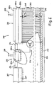
Figuren 4 bis 6dargestellt. Dieser umfasst ebenfalls einen Kontaktbereich 203 mit einem metallischen Kontakt 203a einer darunter befindlichen stark dotieren p-Wanne 203b und einer darunter befindlichen weiteren p-dotierten Schicht 203c. - Das eigentliche Substrat 202 wiederum ist schwach n-dotiert. Der Kontaktbereich 203 wird umgeben von einem Guardring 205. Dieser umfasst eine metallische Kontaktierung sowie eine stark n-dotierte Wanne 205a und eine weitere n-dotierte Schicht 205b, welche unter der Wanne liegt. Ferner ist eine Bias-Schicht 204, die stark p-dotiert ist, auf der Rückseite aufgebracht, sowie eine Passivierungsschicht 213. Eine entsprechende CMOS-Struktur 207 mit einer darunter befindlichen, ebenfalls abschirmenden, p-dotierten Schicht 207' ist ebenso vorhanden. Im Unterschied zu den vorherigen Strukturen ist insbesondere der Guardring von einer Grabenisolation 214 (engl.: shallow-trench isolation, STI) innen (also zum Kontaktbereich hin) und außen (das heißt zu den weiteren Bereichen wie zum Beispiel im CMOS-Bereich hin) umgeben. Diese STI-Struktur dient der stärkeren Abgrenzung der einzelnen Bereiche. Die Kontaktierung der Struktur erfolgt in gewohnter Weise, das heißt der Minuspol 208 wird an dem Kontaktbereich 203 angelegt, während der Pluspol 209 an den Guardring 205 angelegt wird.
- In
Figur 6 sind lediglich zur besseren Erläuterung schematische Ersatzschaltbilder 215 und 216 eingefügt. Die gegeneinander geschalteten Dioden 215 verdeutlichen entsprechend die Ausbildung einer Verarmungszone. - Weiterhin sind in den
Figuren 7, 8 und 9 Beispiele dargestellt, wie Kontaktbereiche 303, 403, 503 angeordnet und hinsichtlich ihrer Form ausgebildet sein können.Figur 7 zeigt ein Substrat 302 einer Halbleiterstruktur in Draufsicht mit einem an der Vorderseite angebrachten einzelnen und punktförmig ausgebildeten Kontaktbereich 303.Figur 8 wiederum zeigt mehrere punktförmige Kontatktbereiche 403 auf einem Substrat 402.Figur 9 zeigt einen ringförmigen Kontaktbereich 503 auf einem Substrat 502. - Zusammenfassend ist eine besonders bevorzugte Halbleiterstruktur zur Photonendetektion ist folgendermaßen aufgebaut:
- Sie besitzt ein hochohmiges Substrat, welches aus im Zonenziehverfahren gewonnenem Silizium (Engl.: float-zone silicon) gefertigt ist mit einem spezifischen Widerstand p > 2000 Ω cm. Dieses halbintrinsische Halbleitermaterial ist z.B. dementsprechend (n--)-dotiert. Dieses Substrat wird auf eine Dicke von ca. 50 µm abgedünnt.
- Zudem weist der Halbleiter einen Kontaktbereich an der Vorderseite des Substrats auf. Insbesondere kommt ein Format von 50 µm x 200 µm in Betracht. Wird, wie vorliegend, ein schwach n-dotiertes Substrat gewählt, umfasst der Kontaktbereich ein sog. p-Source/drain-Implantation aus einem (p++)-dotierten Material (spezifischer Flächenwiderstand ca. 100 Ω bzw. 100 Ω /sq., angeordnet im Bereich von 0 nm bis ca. 100 nm), zudem eine p-Wannen-Implantation mit einer (p+)-dotierten Schicht (spezifischer Flächenwiderstand: ca. 1000 Ω /sq., angeordnet im Bereich von ca. 0,1 µm bis 1,0 µm Tiefe). Diese p-Wanne ist so ausgelegt, dass ein Potential von -1 V bis -5 V angelegt werden kann. Außerdem ist eine p-Subimplantiation vorgesehen, welche aus einem (p+)-dotierten Bereich (spezifischer Flächenwiderstand von ca. 1000 Ω /sq., angeordnet in einer Tiefe von ca. 0,7 µm bis 1,5 µm).
- Der Guardring ist ebenfalls auf der Vorderseite des Substrats ausgebildet und umgibt desn Kontaktbereich. Die Breite des Guardrings beträgt vorzugsweise ca. 10 µm, die Distanz zum Kontaktbereich ebenfalls ca. 10 µm. Ferner ist vorzugsweise eine Grabenisolation (STI) mit einer Breite von 10µm innerhalb und außerhalb des Guardrings vorgesehen. Der Guardring umfasst entsprechend eine n-Source/Drain-Implantation aus (n++)-dotiertem Material mit einem spezifischen Flächenwiderstand von weniger als 100 Ω /sq. und einer Tiefe von der Oberfläche an von 100 nm. Zudem umfasst die Guardring-Struktur eine n-Wannen-Implantation aus (n+)-dotiertem Material (spezifischer Flächenwiderstand: ca. 800 Ω /sq., Tiefe ca. 0,7 µm bis 1,5 µm, angeorndet im Bereich von 100 nm bis 1000 nm Tiefe). Die n-Wannen-Implantation ist so ausgebildet, dass eine Isolierspannung von +5 V bis +10 V angelegt werden kann. Ferner ist eine als vergrabenen n-Schicht ausgebildete Implantation (engl.: n-buried layer implant) aus einem (n+)-dotierten Material (spezifischer Flächenwiderstand: ca. 1300 Ω /sq., vorgesehen, Tiefe: ca. 0,5 µm bis 1,0 µm), welche im Bereich von 500 nm bis 700 nm Tiefe liegt). Darunter ist keine weitere Schicht vorgesehen, insbesondere keine direkte Kontaktierung des n-Guardrings mit dem Substrat.
- Weiterhin ist eine Schicht auf der Rückseite (engl.: backside layer) vorgesehen, die vom Kontaktbereich beabstandet ist, jedoch einen lateralen Überlapp mit dem Kontaktbereich bildet. Sie umfasst eine p-Wannen-Implantation ((p+)-dotiert mit einem spezifischen Flächenwiderstand von weniger als 1000 Ω /sq.), welche von der rückseitigen Oberfläche 200 nm tief reicht. An der Oberfläche ist diese Schicht (backside layer) von einer Antireflexschicht (engl.: Anti-reflective coating, ARC layer) aus Nitriden, ZbSiO oder ZbSiNi) bedeckt. Die rückseitige Schicht ist regelmäßig homogen ausgebildet, d.h. ohne Strukturierung und reicht über den gesamten Waferbereich, gegebenenfalls abgesehen von einem schmalen Randbereich, der z.B. nicht abgedünnt und auf der Rückseite bestückt ist.
-
- 1
- Photodetektor
- 2
- Substrat
- 3
- Kontakt
- 4
- Bias-Schicht
- 5
- Guardring
- 6
- CCD-Bereich
- 7
- CMOS-Bereich
- 8
- Minuspol
- 9
- Pluspol
- 10
- Potentiallinien
- 10'
- Leitungskanal
- 11
- Dioden-Ersatzschaltbild
- 12
- Transistor-Ersatzschaltbild
- 101
- Photodetektor
- 102
- Substrat
- 103
- Kontaktbereich
- 103a
- Metallkontakt
- 103b
- p-Wanne
- 103c
- (p+)-Schicht
- 104
- Bias-Schicht
- 105
- Guardring
- 105a
- (n+)-Wanne
- 105b
- (n+)-Schicht
- 106
- CCD-Bereich
- 107
- CMOS-Bereich
- 108
- Minuspol
- 109
- Pluspol
- 110
- Potentiallinie
- 100'
- Leitungskanal
- 113
- Passivierung
- 201
- Photodetektor
- 202
- Substrat
- 203
- Kontaktbereich
- 203a
- Metallkontakt
- 203b
- p-Wanne
- 203c
- p-Schicht
- 204
- Bias-Schicht
- 205
- Guardring
- 205a
- (n+)-Wanne
- 205b
- (n+)-Schicht
- 207
- CMOS-Bereich
- 207'
- p-Schicht
- 208
- Minuspol
- 209
- Pluspol
- 213
- Passivierung
- 214
- Grabenisolation
- 215
- Dioden-Ersatzschaltbild
- 216
- Transistor-Ersatzschaltbild
- 302
- Substrat
- 303
- Kontaktbereich
- 402
- Substrat
- 403
- Kontaktbereich
- 502
- Substrat
- 503
- Kontaktbereich
Claims (16)
- Halbleiterstruktur (1, 101, 201) zur Photonendetektion, umfassend:- ein Substrat (2, 102, 202, 302, 402, 502) aus einem Halbleitermaterial mit einer Dotierung erster Art,- einen Kontaktbereich (3, 103, 203, 303, 403, 503), der an der Vorderseite des Substrates angebracht ist,- eine Bias-Schicht (4, 104, 204) aus einem Halbleitermaterial mit einer zweiten Dotierung, welche auf der Rückseite des Substrats beabstandet vom Kontaktbereich angeordnet ist, wobei der Kontaktbereich wenigstens teilweise der Bias-Schicht gegenüber liegt, so dass in lateraler Richtung ein Überlappbereich vorhanden ist,- ein Guardring (5, 105, 205), der an der Vorderseite des Substrats angeordnet ist und den Kontaktbereich umgibt,wobei zwischen dem Kontaktbereich und dem Guardring eine Sperrspannung anlegbar ist, dadurch gekennzeichnet, dass der Überlappbereich eine laterale Ausdehnung aufweist, die wenigstens ein Viertel der Distanz zwischen Kontaktbereich und Bias-Schicht beträgt.
- Halbleiterstruktur nach einem der vorgenannten Ansprüche, dadurch gekennzeichnet, dass der Kontaktbereich dazu ausgebildet ist, durch das an ihn angelegte Potential das Potential der Bias-Schicht zu beeinflussen.
- Halbleiterstruktur nach einem der vorgenannten Ansprüche, dadurch gekennzeichnet, dass die Distanz zwischen Kontaktbereich und Bias-Schicht der Dicke des Substrats entspricht.
- Halbleiterstruktur nach einem der vorgenannten Ansprüche, dadurch gekennzeichnet, dass der Kontaktbereich eine im Substrat ausgebildete Wanne (103b, 203b) umfasst, welche ungleichnamig zur Dotierung erster Art dotiert ist.
- Halbleiterstruktur nach einem der vorgenannten Ansprüche, dadurch gekennzeichnet, dass das Substrat hochohmig, insbesondere schwach dotiert ist.
- Halbleiterstruktur nach einem der vorgenannten Ansprüche, dadurch gekennzeichnet, dass der Kontaktbereich im Vergleich zum Substrat ungleichnamig dotiert ist.
- Halbleiterstruktur nach einem der vorgenannten Ansprüche, dadurch gekennzeichnet, dass die Bias-Schicht im Vergleich zum Substrat ungleichnamig dotiert ist.
- Halbleiterstruktur nach einem der vorgenannten Ansprüche, dadurch gekennzeichnet, dass der Guardring eine gleichnamige Dotierung aufweist wie das Substrat.
- Halbleiterstruktur nach einem der vorgenannten Ansprüche, dadurch gekennzeichnet, dass der Guardring stärker dotiert ist als das Substrat.
- Halbleiterstruktur nach einem der vorgenannten Ansprüche, dadurch gekennzeichnet, dass die Halbleiterstruktur dazu ausgebildet ist, von der Rückseite beleuchtet zu werden.
- Halbleiterstruktur nach einem der vorgenannten Ansprüche, dadurch gekennzeichnet, dass lateral versetzt zum Kontaktbereich wenigstens ein weiterer Bereich (6, 7; 106, 107; 207) angeordnet ist, der wenigstens eine Wanne aus einem gleichnamig dotierten Material wie der Kontaktbereich umfasst.
- Halbleiterstruktür nach einem der vorgenannten Ansprüche, dadurch gekennzeichnet, dass wenigstens einer der weiteren Bereiche (6, 106) als Sensorbauteil zur Detektion von Photonen ausgebildet ist.
- Halbleiterstruktur nach einem der vorgenannten Ansprüche, dadurch gekennzeichnet, dass die Halbleiterstruktur dazu ausgebildet ist, dass Photonen wenigstens teilweise in einen Absorptionsbereich des Substrates zur Absorption von Photonen eindringen können, der zum Überlappbereich lateral versetzt ist.
- Halbleiterstruktur nach einem der vorgenannten Ansprüche, dadurch gekennzeichnet, dass die Halbleiterstruktur so ausgebildet ist, dass der Absorptionsbereich bei Anlegen der Sperrspannung eine Verarmungszone bildet.
- Halbleiterstruktur nach einem der vorgenannten Ansprüche, dadurch gekennzeichnet, dass das Substrat aus im Zonenziehverfahren gewonnenem Silizium (engl.: float-zone silicon) gefertigt ist.
- Halbleiterstruktur nach einem der vorgenannten Ansprüche, dadurch gekennzeichnet, dass zwischen dem Kontaktbereich und dem Guardring und/oder zwischen dem Kontaktbereich und dem wenigstens einen weiteren Bereich teilweise eine Grabenisolation (214) (engl.: shallow-trench isolation, STI) angeordnet ist.
Priority Applications (6)
| Application Number | Priority Date | Filing Date | Title |
|---|---|---|---|
| EP11006012.6A EP2549536B1 (de) | 2011-07-22 | 2011-07-22 | Halbleiterstruktur zur Photonendetektion |
| IL220990A IL220990A (en) | 2011-07-22 | 2012-07-17 | Semiconductor structure for photon detection |
| US13/551,732 US8901690B2 (en) | 2011-07-22 | 2012-07-18 | Semiconductor structure for photon detection |
| SG2012053526A SG187357A1 (en) | 2011-07-22 | 2012-07-19 | Semiconductor structure for photon detection |
| CN201210319474.3A CN102891154B (zh) | 2011-07-22 | 2012-07-20 | 用于光子检测的半导体结构 |
| KR1020120079885A KR102114198B1 (ko) | 2011-07-22 | 2012-07-23 | 광자 검출을 위한 반도체 구조체 |
Applications Claiming Priority (1)
| Application Number | Priority Date | Filing Date | Title |
|---|---|---|---|
| EP11006012.6A EP2549536B1 (de) | 2011-07-22 | 2011-07-22 | Halbleiterstruktur zur Photonendetektion |
Related Child Applications (1)
| Application Number | Title | Priority Date | Filing Date |
|---|---|---|---|
| EP19213586.1 Division-Into | 2019-12-04 |
Publications (2)
| Publication Number | Publication Date |
|---|---|
| EP2549536A1 true EP2549536A1 (de) | 2013-01-23 |
| EP2549536B1 EP2549536B1 (de) | 2020-08-19 |
Family
ID=44581941
Family Applications (1)
| Application Number | Title | Priority Date | Filing Date |
|---|---|---|---|
| EP11006012.6A Active EP2549536B1 (de) | 2011-07-22 | 2011-07-22 | Halbleiterstruktur zur Photonendetektion |
Country Status (6)
| Country | Link |
|---|---|
| US (1) | US8901690B2 (de) |
| EP (1) | EP2549536B1 (de) |
| KR (1) | KR102114198B1 (de) |
| CN (1) | CN102891154B (de) |
| IL (1) | IL220990A (de) |
| SG (1) | SG187357A1 (de) |
Families Citing this family (7)
| Publication number | Priority date | Publication date | Assignee | Title |
|---|---|---|---|---|
| JP6045873B2 (ja) * | 2012-10-05 | 2016-12-14 | ルネサスエレクトロニクス株式会社 | 半導体装置の製造方法 |
| US11114480B2 (en) * | 2013-03-15 | 2021-09-07 | ActLight SA | Photodetector |
| DE102016111836B4 (de) * | 2016-06-28 | 2024-02-15 | Infineon Technologies Ag | Halbleiterbauelemente und Verfahren zum Bilden eines Halbleiterbauelements |
| IT201700122669A1 (it) * | 2017-10-27 | 2019-04-27 | Lfoundry Srl | Sensore integrato di radiazione ionizzante e di particelle ionizzanti |
| US11389125B1 (en) * | 2021-02-05 | 2022-07-19 | GE Precision Healthcare LLC | System and method for mitigating trace triggering of channels in x-ray detector |
| US20250015083A1 (en) * | 2021-11-01 | 2025-01-09 | Wesley Harold Morris | Shallow Buried Guard Ring (SBGR) Isolation Structures and Fabrication Models to Enable Latchup Immunity in CMOS Integrated Circuits Operating in Extreme Radiation Environments and Temperatures Ranges |
| US12474453B2 (en) | 2022-01-20 | 2025-11-18 | ActLight SA | Control techniques for photodetector systems |
Citations (6)
| Publication number | Priority date | Publication date | Assignee | Title |
|---|---|---|---|---|
| US5786609A (en) | 1993-09-15 | 1998-07-28 | Max-Planck-Gesellschaft Zur Foerderung Der Wissenschaflen E.V. | Integrated horizontal unipolar transistor having a doped layer forming an internal gate of the transistor and at least one integrated capacitor having a first electrode connected to a source of the transistor and a second electrode to the fixed potential |
| JP2005150521A (ja) * | 2003-11-18 | 2005-06-09 | Canon Inc | 撮像装置およびその製造方法 |
| US20080265295A1 (en) * | 2007-04-27 | 2008-10-30 | Brady Frederick T | Methods, structures and sytems for an image sensor device for improving quantum efficiency of red pixels |
| EP1995783A2 (de) * | 2007-05-24 | 2008-11-26 | Sony Corporation | Festkörperabbildungsvorrichtung und Kamera |
| US20100014675A1 (en) * | 2008-07-15 | 2010-01-21 | The Mitre Corporation | Appraising Systems With Zero Knowledge Proofs |
| WO2010053881A1 (en) * | 2008-11-04 | 2010-05-14 | Array Optronix, Inc. | Devices and methods for ultra thin photodiode arrays on bonded supports |
Family Cites Families (14)
| Publication number | Priority date | Publication date | Assignee | Title |
|---|---|---|---|---|
| US5146296A (en) * | 1987-12-03 | 1992-09-08 | Xsirius Photonics, Inc. | Devices for detecting and/or imaging single photoelectron |
| GB2367945B (en) * | 2000-08-16 | 2004-10-20 | Secr Defence | Photodetector circuit |
| GB0216069D0 (en) * | 2002-07-11 | 2002-08-21 | Qinetiq Ltd | Photodetector circuits |
| TWI228320B (en) * | 2003-09-09 | 2005-02-21 | Ind Tech Res Inst | An avalanche photo-detector(APD) with high saturation power, high gain-bandwidth product |
| US7170143B2 (en) * | 2003-10-20 | 2007-01-30 | Hamamatsu Photonics K.K. | Semiconductor photo-detection device and radiation apparatus |
| US8093633B2 (en) * | 2004-02-17 | 2012-01-10 | Nanyang Technological University | Method and device for wavelength-sensitive photo-sensing |
| JP4841834B2 (ja) * | 2004-12-24 | 2011-12-21 | 浜松ホトニクス株式会社 | ホトダイオードアレイ |
| US7576371B1 (en) * | 2006-03-03 | 2009-08-18 | Array Optronix, Inc. | Structures and methods to improve the crosstalk between adjacent pixels of back-illuminated photodiode arrays |
| KR100959435B1 (ko) * | 2007-12-26 | 2010-05-25 | 주식회사 동부하이텍 | 이미지 센서 및 그 제조방법 |
| ITTO20080046A1 (it) * | 2008-01-18 | 2009-07-19 | St Microelectronics Srl | Schiera di fotodiodi operanti in modalita' geiger reciprocamente isolati e relativo procedimento di fabbricazione |
| EP2455985A3 (de) * | 2008-07-10 | 2013-07-17 | STMicroelectronics (Research & Development) Limited | Verbesserungen von Einzelphoton-Avalanche-Dioden |
| IT1392366B1 (it) * | 2008-12-17 | 2012-02-28 | St Microelectronics Rousset | Fotodiodo operante in modalita' geiger con resistore di soppressione integrato e controllabile, schiera di fotodiodi e relativo procedimento di fabbricazione |
| US8614112B2 (en) * | 2010-10-01 | 2013-12-24 | Omnivision Technologies, Inc. | Method of damage-free impurity doping for CMOS image sensors |
| JP2012164765A (ja) * | 2011-02-04 | 2012-08-30 | Rohm Co Ltd | 半導体装置 |
-
2011
- 2011-07-22 EP EP11006012.6A patent/EP2549536B1/de active Active
-
2012
- 2012-07-17 IL IL220990A patent/IL220990A/en active IP Right Grant
- 2012-07-18 US US13/551,732 patent/US8901690B2/en active Active
- 2012-07-19 SG SG2012053526A patent/SG187357A1/en unknown
- 2012-07-20 CN CN201210319474.3A patent/CN102891154B/zh not_active Expired - Fee Related
- 2012-07-23 KR KR1020120079885A patent/KR102114198B1/ko not_active Expired - Fee Related
Patent Citations (6)
| Publication number | Priority date | Publication date | Assignee | Title |
|---|---|---|---|---|
| US5786609A (en) | 1993-09-15 | 1998-07-28 | Max-Planck-Gesellschaft Zur Foerderung Der Wissenschaflen E.V. | Integrated horizontal unipolar transistor having a doped layer forming an internal gate of the transistor and at least one integrated capacitor having a first electrode connected to a source of the transistor and a second electrode to the fixed potential |
| JP2005150521A (ja) * | 2003-11-18 | 2005-06-09 | Canon Inc | 撮像装置およびその製造方法 |
| US20080265295A1 (en) * | 2007-04-27 | 2008-10-30 | Brady Frederick T | Methods, structures and sytems for an image sensor device for improving quantum efficiency of red pixels |
| EP1995783A2 (de) * | 2007-05-24 | 2008-11-26 | Sony Corporation | Festkörperabbildungsvorrichtung und Kamera |
| US20100014675A1 (en) * | 2008-07-15 | 2010-01-21 | The Mitre Corporation | Appraising Systems With Zero Knowledge Proofs |
| WO2010053881A1 (en) * | 2008-11-04 | 2010-05-14 | Array Optronix, Inc. | Devices and methods for ultra thin photodiode arrays on bonded supports |
Non-Patent Citations (1)
| Title |
|---|
| GROOM D E ET AL: "Back-illuminated, fully-depleted CCD image sensors for use in optical and near-IR astronomy", NUCLEAR INSTRUMENTS & METHODS IN PHYSICS RESEARCH. SECTION A: ACCELERATORS, SPECTROMETERS, DETECTORS, AND ASSOCIATED EQUIPMENT, ELSEVIER BV * NORTH-HOLLAND, NETHERLANDS, vol. 442, no. 1-3, 1 March 2000 (2000-03-01), pages 216 - 222, XP004193493, ISSN: 0168-9002, DOI: 10.1016/S0168-9002(99)01224-3 * |
Also Published As
| Publication number | Publication date |
|---|---|
| KR20130011997A (ko) | 2013-01-30 |
| US8901690B2 (en) | 2014-12-02 |
| SG187357A1 (en) | 2013-02-28 |
| KR102114198B1 (ko) | 2020-05-26 |
| US20130037899A1 (en) | 2013-02-14 |
| CN102891154A (zh) | 2013-01-23 |
| IL220990A (en) | 2017-02-28 |
| CN102891154B (zh) | 2017-06-09 |
| EP2549536B1 (de) | 2020-08-19 |
Similar Documents
| Publication | Publication Date | Title |
|---|---|---|
| EP2549536B1 (de) | Halbleiterstruktur zur Photonendetektion | |
| EP3948951B1 (de) | Avalanche-photodioden-array | |
| EP1241710B1 (de) | Lichtsensitives Halbleiterbauelement | |
| DE102022005196B4 (de) | Verbesserter halbleiter-lichtsensor | |
| EP2629340B1 (de) | Halbleiterstruktur für einen auf dem Lawineneffekt beruhenden Strahlungsdetektor sowie Strahlungsdetektor | |
| DE102016117264A1 (de) | Leistungshalbleiterbauelement mit Steuerbarkeit von dU/dt | |
| DE102016123037A1 (de) | Optischer Sensor mit zwei Abgriffen für photonen-generierte Elektronen des sichtbaren Lichts und des IR Lichts | |
| DE102009017505B4 (de) | Strahlungsdetektor, Verwendung eines Strahlungsdetektors und Verfahren zur Herstellung eines Strahlungsdetektors | |
| WO2004025739A2 (de) | Verfahren zum herstellen einer integrierten pin-diode und zugehörige schaltungsanordnung | |
| WO2022161991A1 (de) | Lawinenfotodiode mit orthogonalem schichtaufbau | |
| EP0902982B1 (de) | Streifendetektor | |
| DE102016111836B4 (de) | Halbleiterbauelemente und Verfahren zum Bilden eines Halbleiterbauelements | |
| DE112021005507T5 (de) | Optischer Sensor | |
| DE102004053077B4 (de) | Vertikale PIN-Fotodiode und Verfahren zur Herstellung, kompatibel zu einem konventionellen CMOS-Prozess | |
| DE19933162B4 (de) | Bildzelle, Bildsensor und Herstellungsverfahren hierfür | |
| DE10308626B4 (de) | Verfahren zur Herstellung von Halbleiter-Strahlungsdetektoren und Halbleiter-Strahlungsdetektor | |
| DE102005007358B4 (de) | Lichtempfindliches Bauelement | |
| DE112021004929B4 (de) | Fotosensorzelle, fotosensor und verfahren | |
| DE112020007122T5 (de) | Fotodiode und verfahren zum betrieb einer fotodiode | |
| DE102013211836B4 (de) | Elektrische Vorrichtungen, Übergangsspannungs-Suppressordiode und Verfahren zur Herstellung einer elektrischen Vorrichtung | |
| EP4531117A1 (de) | Verfahren zur erzeugung tiefliegender p-n-übergänge in einem bcd-prozess, bcd-substrat und darauf basierende einzelphotonen-lawinendiode | |
| WO2025061844A1 (de) | Verfahren zur erzeugung tiefliegender p-n-übergänge in einem bcd-prozess, bcd-substrat und darauf basierende einzelphotonen-lawinendiode | |
| WO2010094374A1 (de) | Photosensor und photosensormatrix | |
| DE10230225A1 (de) | Photomischdetektor und Verfahren zu seinem Betrieb und zu seiner Herstellung | |
| EP1622206A1 (de) | Halbleiter-Strahlungsdetektoren und Verfahren zur Herstellung derselben |
Legal Events
| Date | Code | Title | Description |
|---|---|---|---|
| PUAI | Public reference made under article 153(3) epc to a published international application that has entered the european phase |
Free format text: ORIGINAL CODE: 0009012 |
|
| 17P | Request for examination filed |
Effective date: 20110811 |
|
| AK | Designated contracting states |
Kind code of ref document: A1 Designated state(s): AL AT BE BG CH CY CZ DE DK EE ES FI FR GB GR HR HU IE IS IT LI LT LU LV MC MK MT NL NO PL PT RO RS SE SI SK SM TR |
|
| AX | Request for extension of the european patent |
Extension state: BA ME |
|
| REG | Reference to a national code |
Ref country code: HK Ref legal event code: DE Ref document number: 1178319 Country of ref document: HK |
|
| APBK | Appeal reference recorded |
Free format text: ORIGINAL CODE: EPIDOSNREFNE |
|
| APBN | Date of receipt of notice of appeal recorded |
Free format text: ORIGINAL CODE: EPIDOSNNOA2E |
|
| APBR | Date of receipt of statement of grounds of appeal recorded |
Free format text: ORIGINAL CODE: EPIDOSNNOA3E |
|
| APAF | Appeal reference modified |
Free format text: ORIGINAL CODE: EPIDOSCREFNE |
|
| RIN1 | Information on inventor provided before grant (corrected) |
Inventor name: ANNESE, MARCO Inventor name: DE COI, BEAT Inventor name: POPP, MARTIN |
|
| APBT | Appeal procedure closed |
Free format text: ORIGINAL CODE: EPIDOSNNOA9E |
|
| GRAP | Despatch of communication of intention to grant a patent |
Free format text: ORIGINAL CODE: EPIDOSNIGR1 |
|
| STAA | Information on the status of an ep patent application or granted ep patent |
Free format text: STATUS: GRANT OF PATENT IS INTENDED |
|
| INTG | Intention to grant announced |
Effective date: 20200323 |
|
| GRAS | Grant fee paid |
Free format text: ORIGINAL CODE: EPIDOSNIGR3 |
|
| GRAA | (expected) grant |
Free format text: ORIGINAL CODE: 0009210 |
|
| STAA | Information on the status of an ep patent application or granted ep patent |
Free format text: STATUS: THE PATENT HAS BEEN GRANTED |
|
| AK | Designated contracting states |
Kind code of ref document: B1 Designated state(s): AL AT BE BG CH CY CZ DE DK EE ES FI FR GB GR HR HU IE IS IT LI LT LU LV MC MK MT NL NO PL PT RO RS SE SI SK SM TR |
|
| REG | Reference to a national code |
Ref country code: GB Ref legal event code: FG4D Free format text: NOT ENGLISH |
|
| REG | Reference to a national code |
Ref country code: CH Ref legal event code: EP |
|
| REG | Reference to a national code |
Ref country code: DE Ref legal event code: R096 Ref document number: 502011016866 Country of ref document: DE |
|
| REG | Reference to a national code |
Ref country code: AT Ref legal event code: REF Ref document number: 1304918 Country of ref document: AT Kind code of ref document: T Effective date: 20200915 |
|
| REG | Reference to a national code |
Ref country code: IE Ref legal event code: FG4D Free format text: LANGUAGE OF EP DOCUMENT: GERMAN |
|
| REG | Reference to a national code |
Ref country code: CH Ref legal event code: NV Representative=s name: DENNEMEYER AG, CH |
|
| REG | Reference to a national code |
Ref country code: LT Ref legal event code: MG4D |
|
| REG | Reference to a national code |
Ref country code: NL Ref legal event code: MP Effective date: 20200819 |
|
| PG25 | Lapsed in a contracting state [announced via postgrant information from national office to epo] |
Ref country code: FI Free format text: LAPSE BECAUSE OF FAILURE TO SUBMIT A TRANSLATION OF THE DESCRIPTION OR TO PAY THE FEE WITHIN THE PRESCRIBED TIME-LIMIT Effective date: 20200819 Ref country code: SE Free format text: LAPSE BECAUSE OF FAILURE TO SUBMIT A TRANSLATION OF THE DESCRIPTION OR TO PAY THE FEE WITHIN THE PRESCRIBED TIME-LIMIT Effective date: 20200819 Ref country code: HR Free format text: LAPSE BECAUSE OF FAILURE TO SUBMIT A TRANSLATION OF THE DESCRIPTION OR TO PAY THE FEE WITHIN THE PRESCRIBED TIME-LIMIT Effective date: 20200819 Ref country code: LT Free format text: LAPSE BECAUSE OF FAILURE TO SUBMIT A TRANSLATION OF THE DESCRIPTION OR TO PAY THE FEE WITHIN THE PRESCRIBED TIME-LIMIT Effective date: 20200819 Ref country code: PT Free format text: LAPSE BECAUSE OF FAILURE TO SUBMIT A TRANSLATION OF THE DESCRIPTION OR TO PAY THE FEE WITHIN THE PRESCRIBED TIME-LIMIT Effective date: 20201221 Ref country code: NO Free format text: LAPSE BECAUSE OF FAILURE TO SUBMIT A TRANSLATION OF THE DESCRIPTION OR TO PAY THE FEE WITHIN THE PRESCRIBED TIME-LIMIT Effective date: 20201119 Ref country code: GR Free format text: LAPSE BECAUSE OF FAILURE TO SUBMIT A TRANSLATION OF THE DESCRIPTION OR TO PAY THE FEE WITHIN THE PRESCRIBED TIME-LIMIT Effective date: 20201120 Ref country code: BG Free format text: LAPSE BECAUSE OF FAILURE TO SUBMIT A TRANSLATION OF THE DESCRIPTION OR TO PAY THE FEE WITHIN THE PRESCRIBED TIME-LIMIT Effective date: 20201119 |
|
| PG25 | Lapsed in a contracting state [announced via postgrant information from national office to epo] |
Ref country code: NL Free format text: LAPSE BECAUSE OF FAILURE TO SUBMIT A TRANSLATION OF THE DESCRIPTION OR TO PAY THE FEE WITHIN THE PRESCRIBED TIME-LIMIT Effective date: 20200819 Ref country code: RS Free format text: LAPSE BECAUSE OF FAILURE TO SUBMIT A TRANSLATION OF THE DESCRIPTION OR TO PAY THE FEE WITHIN THE PRESCRIBED TIME-LIMIT Effective date: 20200819 Ref country code: LV Free format text: LAPSE BECAUSE OF FAILURE TO SUBMIT A TRANSLATION OF THE DESCRIPTION OR TO PAY THE FEE WITHIN THE PRESCRIBED TIME-LIMIT Effective date: 20200819 Ref country code: PL Free format text: LAPSE BECAUSE OF FAILURE TO SUBMIT A TRANSLATION OF THE DESCRIPTION OR TO PAY THE FEE WITHIN THE PRESCRIBED TIME-LIMIT Effective date: 20200819 Ref country code: IS Free format text: LAPSE BECAUSE OF FAILURE TO SUBMIT A TRANSLATION OF THE DESCRIPTION OR TO PAY THE FEE WITHIN THE PRESCRIBED TIME-LIMIT Effective date: 20201219 |
|
| PG25 | Lapsed in a contracting state [announced via postgrant information from national office to epo] |
Ref country code: SM Free format text: LAPSE BECAUSE OF FAILURE TO SUBMIT A TRANSLATION OF THE DESCRIPTION OR TO PAY THE FEE WITHIN THE PRESCRIBED TIME-LIMIT Effective date: 20200819 Ref country code: RO Free format text: LAPSE BECAUSE OF FAILURE TO SUBMIT A TRANSLATION OF THE DESCRIPTION OR TO PAY THE FEE WITHIN THE PRESCRIBED TIME-LIMIT Effective date: 20200819 Ref country code: EE Free format text: LAPSE BECAUSE OF FAILURE TO SUBMIT A TRANSLATION OF THE DESCRIPTION OR TO PAY THE FEE WITHIN THE PRESCRIBED TIME-LIMIT Effective date: 20200819 Ref country code: CZ Free format text: LAPSE BECAUSE OF FAILURE TO SUBMIT A TRANSLATION OF THE DESCRIPTION OR TO PAY THE FEE WITHIN THE PRESCRIBED TIME-LIMIT Effective date: 20200819 Ref country code: DK Free format text: LAPSE BECAUSE OF FAILURE TO SUBMIT A TRANSLATION OF THE DESCRIPTION OR TO PAY THE FEE WITHIN THE PRESCRIBED TIME-LIMIT Effective date: 20200819 |
|
| REG | Reference to a national code |
Ref country code: DE Ref legal event code: R097 Ref document number: 502011016866 Country of ref document: DE |
|
| PG25 | Lapsed in a contracting state [announced via postgrant information from national office to epo] |
Ref country code: AL Free format text: LAPSE BECAUSE OF FAILURE TO SUBMIT A TRANSLATION OF THE DESCRIPTION OR TO PAY THE FEE WITHIN THE PRESCRIBED TIME-LIMIT Effective date: 20200819 Ref country code: ES Free format text: LAPSE BECAUSE OF FAILURE TO SUBMIT A TRANSLATION OF THE DESCRIPTION OR TO PAY THE FEE WITHIN THE PRESCRIBED TIME-LIMIT Effective date: 20200819 |
|
| PLBE | No opposition filed within time limit |
Free format text: ORIGINAL CODE: 0009261 |
|
| STAA | Information on the status of an ep patent application or granted ep patent |
Free format text: STATUS: NO OPPOSITION FILED WITHIN TIME LIMIT |
|
| PG25 | Lapsed in a contracting state [announced via postgrant information from national office to epo] |
Ref country code: SK Free format text: LAPSE BECAUSE OF FAILURE TO SUBMIT A TRANSLATION OF THE DESCRIPTION OR TO PAY THE FEE WITHIN THE PRESCRIBED TIME-LIMIT Effective date: 20200819 |
|
| 26N | No opposition filed |
Effective date: 20210520 |
|
| PG25 | Lapsed in a contracting state [announced via postgrant information from national office to epo] |
Ref country code: SI Free format text: LAPSE BECAUSE OF FAILURE TO SUBMIT A TRANSLATION OF THE DESCRIPTION OR TO PAY THE FEE WITHIN THE PRESCRIBED TIME-LIMIT Effective date: 20200819 |
|
| PG25 | Lapsed in a contracting state [announced via postgrant information from national office to epo] |
Ref country code: MC Free format text: LAPSE BECAUSE OF FAILURE TO SUBMIT A TRANSLATION OF THE DESCRIPTION OR TO PAY THE FEE WITHIN THE PRESCRIBED TIME-LIMIT Effective date: 20200819 |
|
| REG | Reference to a national code |
Ref country code: BE Ref legal event code: MM Effective date: 20210731 |
|
| PG25 | Lapsed in a contracting state [announced via postgrant information from national office to epo] |
Ref country code: LU Free format text: LAPSE BECAUSE OF NON-PAYMENT OF DUE FEES Effective date: 20210722 |
|
| PG25 | Lapsed in a contracting state [announced via postgrant information from national office to epo] |
Ref country code: IE Free format text: LAPSE BECAUSE OF NON-PAYMENT OF DUE FEES Effective date: 20210722 Ref country code: BE Free format text: LAPSE BECAUSE OF NON-PAYMENT OF DUE FEES Effective date: 20210731 |
|
| REG | Reference to a national code |
Ref country code: AT Ref legal event code: MM01 Ref document number: 1304918 Country of ref document: AT Kind code of ref document: T Effective date: 20210722 |
|
| PG25 | Lapsed in a contracting state [announced via postgrant information from national office to epo] |
Ref country code: AT Free format text: LAPSE BECAUSE OF NON-PAYMENT OF DUE FEES Effective date: 20210722 |
|
| PG25 | Lapsed in a contracting state [announced via postgrant information from national office to epo] |
Ref country code: HU Free format text: LAPSE BECAUSE OF FAILURE TO SUBMIT A TRANSLATION OF THE DESCRIPTION OR TO PAY THE FEE WITHIN THE PRESCRIBED TIME-LIMIT; INVALID AB INITIO Effective date: 20110722 Ref country code: CY Free format text: LAPSE BECAUSE OF FAILURE TO SUBMIT A TRANSLATION OF THE DESCRIPTION OR TO PAY THE FEE WITHIN THE PRESCRIBED TIME-LIMIT Effective date: 20200819 |
|
| P01 | Opt-out of the competence of the unified patent court (upc) registered |
Effective date: 20230523 |
|
| PGFP | Annual fee paid to national office [announced via postgrant information from national office to epo] |
Ref country code: IT Payment date: 20230731 Year of fee payment: 13 Ref country code: GB Payment date: 20230724 Year of fee payment: 13 |
|
| PGFP | Annual fee paid to national office [announced via postgrant information from national office to epo] |
Ref country code: FR Payment date: 20230724 Year of fee payment: 13 |
|
| PG25 | Lapsed in a contracting state [announced via postgrant information from national office to epo] |
Ref country code: MK Free format text: LAPSE BECAUSE OF FAILURE TO SUBMIT A TRANSLATION OF THE DESCRIPTION OR TO PAY THE FEE WITHIN THE PRESCRIBED TIME-LIMIT Effective date: 20200819 |
|
| PG25 | Lapsed in a contracting state [announced via postgrant information from national office to epo] |
Ref country code: MT Free format text: LAPSE BECAUSE OF FAILURE TO SUBMIT A TRANSLATION OF THE DESCRIPTION OR TO PAY THE FEE WITHIN THE PRESCRIBED TIME-LIMIT Effective date: 20200819 |
|
| REG | Reference to a national code |
Ref country code: DE Ref legal event code: R079 Ref document number: 502011016866 Country of ref document: DE Free format text: PREVIOUS MAIN CLASS: H01L0027146000 Ipc: H10F0039180000 |
|
| REG | Reference to a national code |
Ref country code: DE Ref legal event code: R082 Ref document number: 502011016866 Country of ref document: DE Representative=s name: RAVENSPAT PATENTANWAELTE PARTNERSCHAFT MBB, DE |
|
| GBPC | Gb: european patent ceased through non-payment of renewal fee |
Effective date: 20240722 |
|
| PG25 | Lapsed in a contracting state [announced via postgrant information from national office to epo] |
Ref country code: FR Free format text: LAPSE BECAUSE OF NON-PAYMENT OF DUE FEES Effective date: 20240731 |
|
| PG25 | Lapsed in a contracting state [announced via postgrant information from national office to epo] |
Ref country code: GB Free format text: LAPSE BECAUSE OF NON-PAYMENT OF DUE FEES Effective date: 20240722 |
|
| PG25 | Lapsed in a contracting state [announced via postgrant information from national office to epo] |
Ref country code: IT Free format text: LAPSE BECAUSE OF NON-PAYMENT OF DUE FEES Effective date: 20240722 |
|
| PGFP | Annual fee paid to national office [announced via postgrant information from national office to epo] |
Ref country code: DE Payment date: 20250722 Year of fee payment: 15 |
|
| PGFP | Annual fee paid to national office [announced via postgrant information from national office to epo] |
Ref country code: CH Payment date: 20250801 Year of fee payment: 15 |
|
| PG25 | Lapsed in a contracting state [announced via postgrant information from national office to epo] |
Ref country code: TR Free format text: LAPSE BECAUSE OF FAILURE TO SUBMIT A TRANSLATION OF THE DESCRIPTION OR TO PAY THE FEE WITHIN THE PRESCRIBED TIME-LIMIT Effective date: 20200819 |
|
| REG | Reference to a national code |
Ref country code: CH Ref legal event code: U11 Free format text: ST27 STATUS EVENT CODE: U-0-0-U10-U11 (AS PROVIDED BY THE NATIONAL OFFICE) Effective date: 20260801 |