EP2541602A1 - Lichtemittierende Struktur, Anzeigevorrichtung und Herstellungsverfahren - Google Patents
Lichtemittierende Struktur, Anzeigevorrichtung und Herstellungsverfahren Download PDFInfo
- Publication number
- EP2541602A1 EP2541602A1 EP20120156715 EP12156715A EP2541602A1 EP 2541602 A1 EP2541602 A1 EP 2541602A1 EP 20120156715 EP20120156715 EP 20120156715 EP 12156715 A EP12156715 A EP 12156715A EP 2541602 A1 EP2541602 A1 EP 2541602A1
- Authority
- EP
- European Patent Office
- Prior art keywords
- light emitting
- layer
- sub
- electrode
- pixel region
- Prior art date
- Legal status (The legal status is an assumption and is not a legal conclusion. Google has not performed a legal analysis and makes no representation as to the accuracy of the status listed.)
- Granted
Links
Images




Classifications
-
- H—ELECTRICITY
- H10—SEMICONDUCTOR DEVICES; ELECTRIC SOLID-STATE DEVICES NOT OTHERWISE PROVIDED FOR
- H10K—ORGANIC ELECTRIC SOLID-STATE DEVICES
- H10K59/00—Integrated devices, or assemblies of multiple devices, comprising at least one organic light-emitting element covered by group H10K50/00
- H10K59/30—Devices specially adapted for multicolour light emission
- H10K59/35—Devices specially adapted for multicolour light emission comprising red-green-blue [RGB] subpixels
-
- H—ELECTRICITY
- H10—SEMICONDUCTOR DEVICES; ELECTRIC SOLID-STATE DEVICES NOT OTHERWISE PROVIDED FOR
- H10K—ORGANIC ELECTRIC SOLID-STATE DEVICES
- H10K59/00—Integrated devices, or assemblies of multiple devices, comprising at least one organic light-emitting element covered by group H10K50/00
- H10K59/80—Constructional details
- H10K59/875—Arrangements for extracting light from the devices
- H10K59/876—Arrangements for extracting light from the devices comprising a resonant cavity structure, e.g. Bragg reflector pair
-
- H—ELECTRICITY
- H10—SEMICONDUCTOR DEVICES; ELECTRIC SOLID-STATE DEVICES NOT OTHERWISE PROVIDED FOR
- H10K—ORGANIC ELECTRIC SOLID-STATE DEVICES
- H10K50/00—Organic light-emitting devices
- H10K50/10—OLEDs or polymer light-emitting diodes [PLED]
- H10K50/11—OLEDs or polymer light-emitting diodes [PLED] characterised by the electroluminescent [EL] layers
- H10K50/12—OLEDs or polymer light-emitting diodes [PLED] characterised by the electroluminescent [EL] layers comprising dopants
-
- H—ELECTRICITY
- H10—SEMICONDUCTOR DEVICES; ELECTRIC SOLID-STATE DEVICES NOT OTHERWISE PROVIDED FOR
- H10K—ORGANIC ELECTRIC SOLID-STATE DEVICES
- H10K50/00—Organic light-emitting devices
- H10K50/10—OLEDs or polymer light-emitting diodes [PLED]
- H10K50/11—OLEDs or polymer light-emitting diodes [PLED] characterised by the electroluminescent [EL] layers
- H10K50/125—OLEDs or polymer light-emitting diodes [PLED] characterised by the electroluminescent [EL] layers specially adapted for multicolour light emission, e.g. for emitting white light
- H10K50/13—OLEDs or polymer light-emitting diodes [PLED] characterised by the electroluminescent [EL] layers specially adapted for multicolour light emission, e.g. for emitting white light comprising stacked EL layers within one EL unit
-
- H—ELECTRICITY
- H10—SEMICONDUCTOR DEVICES; ELECTRIC SOLID-STATE DEVICES NOT OTHERWISE PROVIDED FOR
- H10K—ORGANIC ELECTRIC SOLID-STATE DEVICES
- H10K50/00—Organic light-emitting devices
- H10K50/10—OLEDs or polymer light-emitting diodes [PLED]
- H10K50/18—Carrier blocking layers
-
- H—ELECTRICITY
- H10—SEMICONDUCTOR DEVICES; ELECTRIC SOLID-STATE DEVICES NOT OTHERWISE PROVIDED FOR
- H10K—ORGANIC ELECTRIC SOLID-STATE DEVICES
- H10K50/00—Organic light-emitting devices
- H10K50/10—OLEDs or polymer light-emitting diodes [PLED]
- H10K50/19—Tandem OLEDs
-
- H—ELECTRICITY
- H10—SEMICONDUCTOR DEVICES; ELECTRIC SOLID-STATE DEVICES NOT OTHERWISE PROVIDED FOR
- H10K—ORGANIC ELECTRIC SOLID-STATE DEVICES
- H10K50/00—Organic light-emitting devices
- H10K50/80—Constructional details
- H10K50/85—Arrangements for extracting light from the devices
- H10K50/852—Arrangements for extracting light from the devices comprising a resonant cavity structure, e.g. Bragg reflector pair
-
- H—ELECTRICITY
- H10—SEMICONDUCTOR DEVICES; ELECTRIC SOLID-STATE DEVICES NOT OTHERWISE PROVIDED FOR
- H10K—ORGANIC ELECTRIC SOLID-STATE DEVICES
- H10K59/00—Integrated devices, or assemblies of multiple devices, comprising at least one organic light-emitting element covered by group H10K50/00
- H10K59/10—OLED displays
- H10K59/12—Active-matrix OLED [AMOLED] displays
- H10K59/126—Shielding, e.g. light-blocking means over the TFTs
-
- H—ELECTRICITY
- H10—SEMICONDUCTOR DEVICES; ELECTRIC SOLID-STATE DEVICES NOT OTHERWISE PROVIDED FOR
- H10K—ORGANIC ELECTRIC SOLID-STATE DEVICES
- H10K71/00—Manufacture or treatment specially adapted for the organic devices covered by this subclass
- H10K71/10—Deposition of organic active material
- H10K71/18—Deposition of organic active material using non-liquid printing techniques, e.g. thermal transfer printing from a donor sheet
-
- H—ELECTRICITY
- H10—SEMICONDUCTOR DEVICES; ELECTRIC SOLID-STATE DEVICES NOT OTHERWISE PROVIDED FOR
- H10K—ORGANIC ELECTRIC SOLID-STATE DEVICES
- H10K50/00—Organic light-emitting devices
- H10K50/10—OLEDs or polymer light-emitting diodes [PLED]
- H10K50/18—Carrier blocking layers
- H10K50/181—Electron blocking layers
-
- H—ELECTRICITY
- H10—SEMICONDUCTOR DEVICES; ELECTRIC SOLID-STATE DEVICES NOT OTHERWISE PROVIDED FOR
- H10K—ORGANIC ELECTRIC SOLID-STATE DEVICES
- H10K59/00—Integrated devices, or assemblies of multiple devices, comprising at least one organic light-emitting element covered by group H10K50/00
- H10K59/10—OLED displays
- H10K59/12—Active-matrix OLED [AMOLED] displays
- H10K59/1201—Manufacture or treatment
-
- H—ELECTRICITY
- H10—SEMICONDUCTOR DEVICES; ELECTRIC SOLID-STATE DEVICES NOT OTHERWISE PROVIDED FOR
- H10K—ORGANIC ELECTRIC SOLID-STATE DEVICES
- H10K71/00—Manufacture or treatment specially adapted for the organic devices covered by this subclass
Definitions
- the present invention relates to a light emitting structure, a display device including a light emitting structure, and a method of manufacturing a display device including a light emitting structure.
- An organic light emitting display (OLED) device displays information such as images and characters using light generated from an organic layer therein. Light may be generated by combination of holes from an anode and electrons from a cathode occurring at the organic layer between the anode and the cathode.
- OLED organic light emitting display
- the organic light emitting display device has features such as wide viewing angle, fast response time, thin thickness and low power consumption, so that the organic light emitting display device is widely employed in various electronic apparatuses.
- a conventional organic light emitting display device electrons and holes provided from electrodes may be recombined at an organic layer to generate excitons, so that light having a specific wavelength may be generated by the energy of the excitons to display images.
- the organic light emitting display device may have a single layer structure, a multi-layer structure, or a colour conversion structure, the multi-layer structure is widely applied in the organic light emitting display device.
- the multi-layer structure may include organic layers that emit red light, green light, and blue light, respectively, and thus red, green, and blue lights may be combined to generate white light.
- the conventional organic light emitting display may have some disadvantages such as relatively low functional stability of the organic layers and low purity of colours of light.
- Example embodiments of the present invention are directed toward a light emitting structure having improved colour purity, enhanced colour reproducibility, and increased brightness, and a display device and method capable of displaying a high resolution image with improved colour purity and enhanced brightness.
- a light emitting structure that includes a first hole injection layer, a first organic light emitting layer, a charge generation layer, a second hole injection layer, a second organic light emitting layer, an electron transfer layer, and a blocking member.
- the light emitting structure may be divided into a first sub-pixel region, a second sub-pixel region, and a third sub-pixel region.
- the first organic light emitting layer may be on the first hole injection layer.
- the charge generation layer may be on the first organic light emitting layer.
- the second hole injection layer may be on the charge generation layer.
- the second organic light emitting layer may be on the second hole injection layer.
- the electron transfer layer may be on the second organic light emitting layer.
- the blocking member may be at at least one of the first sub-pixel region, the second sub-pixel region, or the third sub-pixel region.
- a first optical resonance distance in the first sub-pixel region, a second optical resonance distance in the second sub-pixel region, and a third optical resonance distance in the third sub-pixel region may be different from each other.
- the light emitting structure may include an optical distance controlling insulation layer at at least one of the first sub-pixel region, the second sub-pixel region, or the third sub-pixel region.
- the optical distance controlling insulation layer may be under the first hole injection layer.
- the optical distance controlling insulation layer may have different thicknesses in adjacent sub-pixel regions.
- the optical distance controlling insulation layer may include a material that is the same as that of the first hole injection layer.
- the first optical resonance distance may be adjusted to generate an optical resonance for a red light emitted from the first organic light emitting layer or the second organic light emitting layer
- the second optical resonance distance may be adjusted to generate an optical resonance for a green light emitted from the first organic light emitting layer or the second organic light emitting layer
- the third optical resonance distance may be adjusted to generate an optical resonance for a blue light emitted from the first organic light emitting layer or the second organic light emitting layer.
- the first organic light emitting layer may include a blue-light emitting film
- the second organic light emitting layer may include a green-light emitting film and a red-light emitting film, or a single light emitting film adapted to emit green light and red light.
- the blocking member may be between the second hole injection layer and the first organic light emitting layer at the first sub-pixel region, and the blocking member may be adapted to block a movement of electrons from the second hole injection layer to the first organic light emitting layer at the first sub-pixel region.
- the blocking member may be between the charge generation layer and the first organic light emitting layer at the first sub-pixel region, and the blocking member may be adapted to block a movement of excitons generated at the first organic light emitting layer at the first sub-pixel region.
- the first organic light emitting layer may include a green-light emitting film and a red-light emitting film, or a single light emitting film adapted to emit green light and red light, and the second organic light emitting layer may include a blue-light emitting film.
- the blocking member may be between the second hole injection layer and the second organic light emitting layer at the first sub-pixel region, and the blocking member may be adapted to block a movement of electrons to the second organic light emitting layer at the first sub-pixel region.
- the blocking member may be between the electron transfer layer and the second organic light emitting layer at the first sub-pixel region, and the blocking member may be adapted to block a movement of excitons generated from the second organic light emitting layer at the first sub-pixel region.
- the blocking member may include an electron blocking layer or an exciton quenching layer.
- the blocking member may include materials according to claim 11.
- a display device that includes a substrate, a first electrode, a light emitting structure, and a second electrode.
- the substrate may include a first sub-pixel region, a second sub-pixel region, and a third sub-pixel region.
- the first electrode may be on the substrate.
- the light emitting structure may be on the first electrode.
- the light emitting structure may include a blocking member at at least one of the first sub-pixel region, the second sub-pixel region, or the third sub-pixel region.
- the second electrode may be on the light emitting structure.
- a first optical resonance distance between the first electrode and the second electrode at the first sub-pixel region, a second optical resonance distance between the first electrode and the second electrode at the second sub-pixel region, and a third optical resonance distance between the first electrode and the second electrode at the third sub-pixel region may be different from each other.
- the light emitting structure may include a first hole injection layer, a first organic light emitting layer, a charge generation layer, a second hole injection layer, a second organic light emitting layer, and an electron transfer layer.
- the first hole injection layer may be on the first electrode.
- the first organic light emitting layer may be on the first hole injection layer.
- the charge generation layer may be on the first organic light emitting layer.
- the second hole injection layer may be on the charge generation layer.
- the second organic light emitting layer may be on the second hole injection layer.
- the electron transfer layer may be on the second organic light emitting layer.
- a first electrode may be formed on a substrate.
- the substrate may have a first sub-pixel region, a second sub-pixel region, and a third sub-pixel region.
- a light emitting structure may be formed on the first electrode.
- the light emitting structure may include an optical distance controlling layer and a blocking member.
- a second electrode may be formed on the light emitting structure.
- Forming the light emitting structure may further include forming a first organic light emitting layer on the optical distance controlling insulation layer, forming a charge generation layer on the first organic light emitting layer, and forming a second organic light emitting layer on the charge generation layer.
- the blocking member may be between the optical distance controlling layer and the first organic light emitting layer at at least one of the first, the second, and the third sub-pixel regions.
- the blocking member may be formed by a laser induced thermal imaging process. Forming the blocking member may further include laminating a donor substrate on the substrate, irradiating a laser beam to at least one region of the donor substrate, the at least one region of the donor substrate corresponding to at least one of the first, the second, and the third sub-pixel regions, and removing the donor substrate from the substrate.
- the blocking member may be between the first organic light emitting layer and the charge generation layer at at least one of the first, the second, and the third sub-pixel regions.
- the blocking member may be between the second organic light emitting layer and the second electrode at at least one of the first, the second, and the third sub-pixel regions.
- Each of sub pixel regions may have optical resonance distances which may be substantially different from each other, so that lights having different wavelengths may be emitted from each of the sub-pixel regions. Therefore, colour purity, brightness, and colour gamut of a display device may be improved, and a driving voltage of the display device may be reduced thereby to extend a lifetime of the display device. Further, a blue light emitting layer may be separated from a red light emitting layer and/or a green light emitting layer, so that colour stability may be improved, and a lifetime of the blue light emitting layer may be extended.
- the display device may display high resolution images having high colour purity and high brightness without a colour filter.
- additional layers such as the colour filter may not need to be formed, and thus a cost of the manufacturing process may be reduced, and the manufacturing process may be simplified. Further, the colour filter may not be disposed on the light emitting layers, so that a reduction of the brightness by the colour filter may be prevented.
- the display device includes a substrate 100, a switching structure, a first electrode 300, a light emitting structure 400, a second electrode 500, etc.
- the display device includes a display region where the light emitting structure 400 may be positioned and a non-display region adjacent to the display region.
- the display region of the display device may include a first sub-pixel region (I), a second sub-pixel region (II), and a third sub-pixel region (III).
- the light emitting structure 400 may also have the first sub-pixel region (I), the second sub-pixel region (II), and the third sub-pixel region (III).
- the switching structure may be disposed between the substrate 100 and the first electrode 300, and the light emitting structure 400 may be located between the first electrode 300 and the second electrode 500. In this case, the switching structure may be on the substrate 100.
- a buffer layer 110 may be disposed on the substrate 100.
- the buffer layer 110 may prevent impurities from being diffused from the substrate 100.
- the buffer layer 110 may improve a flatness of the substrate 100. Further, the buffer layer 110 may reduce a stress generated in a process for forming the switching structure on the substrate 100.
- the buffer layer 110 may include an oxide, a nitride, an oxynitride, etc.
- the buffer layer 110 may have a single layer structure or a multi-layer structure including silicon oxide (SiOx), silicon nitride (SiNx) and/or silicon oxynitride (SiOxNy).
- the switching structure may be disposed between the substrate 100 and the first electrode 300.
- the switching structure may include a switching device and one or more insulation layers.
- the switching device may include a thin film transistor having a semiconductor layer containing, for example, silicon.
- the switching device may include an oxide semiconductor device having an active layer containing a semiconductor oxide.
- the switching device may include a semiconductor layer 210, a gate insulation layer 220, a gate electrode 231, a source electrode 233, a drain electrode 235, etc.
- the semiconductor layer 210 may be disposed on the buffer layer 110.
- the gate insulation layer 220 may be positioned on the buffer layer 110 to cover the semiconductor layer 210.
- the semiconductor layer 210 may include a first impurity region 211, a channel region 213, and a second impurity region 215.
- the first impurity region 211 and the second impurity region 215 may serve as a drain region and a source region of the thin film transistor, respectively.
- the semiconductor layer 210 may include a polysilicon, a polysilicon doped with impurities, an amorphous silicon, an amorphous silicon doped with impurities, etc. These may be used alone or in a combination thereof.
- the gate insulation layer 220 may include an oxide, an organic insulation material, etc.
- the gate insulation layer 220 may include silicon oxide, hafnium oxide (HfOx), aluminum oxide (AlOx), zirconium oxide (ZrOx), titanium oxide (TiOx), tantalum oxide (TaOx), a benzocyclobutene (BCB) based resin, an acryl-based resin, etc.
- the gate insulation layer 220 may have a single layer structure or a multi-layer structure including an oxide film and/or an organic insulation material film.
- the gate electrode 231 may be located on the gate insulation layer 220 adjacent to the semiconductor layer 210.
- the gate electrode 231 may be disposed on the gate insulation layer 220 under which the channel region 213 of the semiconductor layer 210 may be positioned.
- the gate electrode 231 may include a metal, a metal nitride, a conductive metal oxide, a transparent conductive material, etc.
- the gate electrode 231 may include aluminum (Al), an alloy containing aluminum, aluminum nitride (AINx), silver (Ag), an alloy containing silver, tungsten (W), tungsten nitride (WNx), copper (Cu), an alloy containing copper, nickel (Ni), chromium (Cr), molybdenum (Mo), an alloy containing molybdenum, titanium (Ti), titanium nitride (TiNx), platinum (Pt), tantalum (Ta), neodymium (Nd), scandium (Sc), tantalum nitride (TaNx), strontium ruthenium oxide (SrRuxOy), zinc oxide (ZnOx), indium tin oxide (ITO), tin oxide (SnOx), indium oxide (InOx), gallium oxide(GaOx), indium zinc oxide (IZO), etc.
- the gate electrode 231 may have a single layer structure or a multi-layer structure including a metal
- a gate line (not illustrated) connected to the gate electrode 231 may be disposed on the gate insulation layer 220.
- a gate signal may be applied to the gate electrode 231 through the gate line.
- the gate line may include a material substantially that is the same as or substantially similar to that of the gate electrode 231.
- the gate line may have a single layer structure or a multi-layer structure including a metal film, a metal nitride film, a conductive metal oxide film, and/or a transparent conductive material film.
- An insulating interlayer 240 may be disposed on the gate insulation layer 220 to cover the gate electrode 231.
- the insulating interlayer 240 may include an oxide, a nitride, an oxynitride, an organic insulation material, etc.
- the insulating interlayer 240 may include silicon oxide, silicon nitride, silicon oxynitride, an acryl-based resin, a polyimide-based resin, a siloxane-based resin, etc. These may be used alone or in a combination thereof.
- the insulating interlayer 240 may have a uniform thickness along a profile of the gate electrode 231. In some example embodiments, the insulating interlayer 240 may cover the gate electrode 231, and may also have a substantially level upper surface.
- the source electrode 233 and the drain electrode 235 may pass through the insulating interlayer 240 and the gate insulation layer 220.
- the source electrode 233 and the drain electrode 235 may make contact with the second impurity region 215 and the first impurity region 211, respectively.
- Each of the source electrode 233 and the drain electrode 235 may include a metal, a metal nitride, a conductive metal oxide, a transparent conductive material, etc.
- the source and the drain electrodes 233 and 235 may include aluminum, an alloy containing aluminum, aluminum nitride, silver, an alloy containing silver, tungsten, tungsten nitride, copper, an alloy containing copper, nickel, chromium, molybdenum, an alloy containing molybdenum, titanium, titanium nitride, platinum, tantalum, neodymium, scandium, tantalum nitride, strontium ruthenium oxide, zinc oxide, indium tin oxide, tin oxide, indium oxide, gallium oxide, indium zinc oxide, etc. These may be used alone or in a combination thereof.
- Each of the source electrode 233 and the drain electrode 235 may have a single layer structure or a multi-layer structure including a metal film, a metal nitride film, a conductive metal oxide film, and/or a transparent conductive material film.
- a data line (not illustrated) connected to the source electrode 233 may be disposed on the insulating interlayer 240, and a data signal may be applied to the source electrode 233 through the data line.
- the data line may include a material that is substantially the same as or substantially similar to that of the source electrode 233. Further, the data line may have a single layer structure or a multi-layer structure including a metal film, a metal nitride film, a conductive metal oxide film, and/or a transparent conductive material film.
- the gate line and the data line may be substantially perpendicular to each other, so that the display region of the display device may be defined by the gate line and the data line.
- An insulation layer 250 of the switching structure may be located on the insulating interlayer 240 to cover the source electrode 233 and the drain electrode 235. A hole may be formed through the insulation layer 250 to partially expose the drain electrode 235.
- the insulation layer 250 may include a transparent insulation material such as a transparent plastic, a transparent resin, etc.
- the insulation layer 250 may include a benzocyclobutene-based resin, an olefin-based resin, a polyimide-based resin, an acryl-based resin, a polyvinyl-based resin, a siloxane-based resin, etc. These may be used alone or in a combination thereof.
- the insulation layer 250 may have a substantially flat upper surface obtained by a planarization process.
- an upper portion of the insulation layer 250 may be planarized by a chemical mechanical polishing (CMP) process, an etch-back process, etc.
- the insulation layer 250 may include a material having a self planarizing property without requiring a planarization process.
- the switching device including the thin film transistor may have a top gate structure in which the gate electrode 231 may be disposed on the semiconductor layer 210, but the configuration of the switching device may not be limited thereto.
- the switching device may have a bottom gate structure in which the gate electrode 231 may be disposed under the semiconductor layer 210, or may include the oxide semiconductor device having the active layer containing a semiconductor oxide.
- the first electrode 300 may be disposed on the insulation layer 250.
- the first electrode 300 may partially or fully fill the hole formed through the insulation layer 250, and thus the first electrode 300 may make electrical contact with the switching device.
- the first electrode 300 may make contact with the drain electrode 235 exposed by the hole.
- a contact (not illustrated), a plug (not illustrated), or a pad (not illustrated) may be additionally disposed on the drain electrode 235 to fill the hole of the insulation layer 250.
- the first electrode 300 may be electrically connected to the drain electrode 235 through the pad, the plug, or the contact.
- the first electrode 300 may serve as a reflective electrode having a suitable reflectivity.
- the second electrode 500 may serve as a transparent electrode having a suitable transmittance or a transflective electrode that is semi-transparent. Materials in the first and the second electrodes 300 and 500 may vary in accordance with an emission type of the display device. For example, the first electrode 300 may serve as a transparent electrode or a transflective electrode, whereas the second electrode 500 may serve as a reflective electrode in case that the display device is a bottom emission type.
- the term “reflective” may indicate an object having a reflectivity of about 70% to about 100% relative to an incident light
- the term “transflective” may indicate an object having a reflectivity of about 30% to about 70% with respect to an incident light
- the term “transparent” may indicate an object having a reflectivity of about 0% to about 30% with respect to an incident light.
- the first electrode 300 when the first electrode 300 serves as the reflective electrode, the first electrode 300 may include a metal and/or an alloy having a relatively high reflectivity.
- the first electrode 300 may include silver (Ag), aluminum (Al), platinum (Pt), gold (Au), chrome (Cr), tungsten (W), molybdenum (Mo), titanium (Ti), palladium (Pa), an alloy thereof, etc. These may be used alone or in a combination thereof.
- the alloy in the first electrode 300 may include an ACA (Ag-Cu-Au) alloy, an APC (Ag-Pd-Cu) alloy, etc.
- the first electrode 300 may have a single layer structure or a multi-layer structure including a metal film and/or an alloy film.
- the second electrode 500 may include a single metal film.
- the second electrode 500 may have a set or predetermined reflectivity and a set or predetermined transmittance.
- the display device may have relatively low luminance efficiency, so that the second electrode 500 should have a relatively thin thickness.
- the second electrode 500 may have a thickness below about 30nm.
- the second electrode 500 may include a metal and/or an alloy such as silver (Ag), aluminum (Al), platinum (Pt), gold (Au), chromium (Cr), tungsten (W), molybdenum (Mo), titanium (Ti), palladium (Pa), alloys of these metals, etc. These may be used alone or in a combination.
- the second electrode 500 may include a transparent conductive material, and thus the second electrode may serve as the transparent electrode.
- the second electrode 500 may include an indium zinc oxide, an indium tin oxide, a gallium-tin oxide, a zinc oxide, a gallium oxide, a tin oxide, an indium oxide, etc. These may be used alone or in a combination thereof.
- the second electrode 500 may have a multi-layer structure including a plurality of the transparent films or a plurality of the transflective films having different reflective indices.
- the first electrode 300 may serve as an anode for providing holes into a first hole injection layer 410 of the light emitting structure 400.
- the second electrode 500 may serve as a cathode for supplying electrons into an electron transfer layer 490.
- functions of the first and the second electrodes 300 and 500 may not be limited thereto, and roles of the first electrode 300 and the second electrode 500 may be modified in accordance with the emission type of the display device.
- a stacked construction (or configuration) having a hole transfer layer, an organic light emitting layer, and an electron transfer layer in the light emitting structure 400 may vary in accordance with the functions of the first electrode 300 and the second electrode 500.
- the display region of the display device may have the first sub-pixel region (I), the second sub-pixel region (II), and the third sub-pixel region (III) as illustrated in FIG. 1 .
- An optical distance controlling insulation layer 350 may be disposed on the first electrode 300 in the display region, and a protection layer 280 may be located on the insulation layer 250 in the non-display region adjacent to the display region.
- the protection layer 280 may extend to partially cover the first electrode 300 that is electrically connected to the drain electrode 235.
- the protection layer 280 may include an oxide, a nitride, an oxynitride, an organic insulation material, etc.
- the protection layer may include silicon oxide, silicon nitride, silicon oxy nitride, a benzocyclobutene-based resin, an olefin-based resin, a polyimide-based resin, an acryl-based resin, a polyvinyl-based resin, a siloxane-based resin, etc. These may be used alone or in a combination thereof.
- the display device may not include the protection layer 280, and thus the display device may have a simpler construction.
- the optical distance controlling insulation layer 350 may be positioned on the first electrode 300 in the first sub-pixel region (I) and the second sub-pixel region (II). In some example embodiments, the optical distance controlling insulation layer 350 may be located on the first electrode 300 in the first sub-pixel region (I), the second sub-pixel region (II), and the third sub-pixel region (III). In other example embodiments, the optical distance controlling insulation layer 350 may be disposed on the first electrode 300 located in at least one of the first sub-pixel region (I), the second sub-pixel region (II), or the third sub-pixel region (III).
- the optical distance controlling insulation layer 350 may adjust or may ensure an optical resonance distance for generating optical resonances of light emitted from the light emitting structure 400.
- the optical distance controlling insulation layer 350 may have various thicknesses substantially different in the first, the second, and the third sub-pixel regions (I, II, and III).
- a first portion of the optical distance controlling insulation layer 350 in the first sub-pixel region (I) may have a thickness that is substantially larger than that of a second portion of the optical distance controlling insulation layer 350 in the second sub-pixel region (II).
- Distances between the first electrode 300 and the second electrode 500 in the first, the second, and the third sub-pixel regions (I, II, and III) may vary depending on the thickness difference of the optical distance controlling insulation layer 350 in the first, the second, and the third sub-pixel regions (I, II, and III).
- the optical distance controlling insulation layer 350 may be substantially transparent.
- the optical distance controlling insulation layer 350 may have a transmittance of about 70% to about 100% relative to an incident light.
- the optical distance controlling insulation layer 350 may include a material that is substantially the same as or substantially similar to that of the first hole injection layer 410.
- the optical distance controlling insulation layer 350 may include a transparent insulation material.
- the optical distance controlling insulation layer 350 may include a benzocyclobutene-based resin, an olefin-based resin, a polyimide-based resin, an acryl-based resin, a polyvinyl-based resin, a siloxane-based resin, etc. These may be used alone or in a combination thereof.
- the term “optical resonance” or “microcavity effect” indicates the increase of luminance and/or intensity of light having a set or predetermined wavelength when an optical distance between two reflective or transflective faces satisfies the conditions of constructive interference of the light having the set or predetermined wavelength.
- the term “reflective” may indicate a reflectivity of about 70% to about 100% relative to an incident light
- the term “transflective” may indicate a reflectivity of about 30% to about 70% with respect to an incident light.
- the optical distance may be substantially equal to a value obtained by multiplying the refraction index (n) of a layer and/or an electrode with the thickness (d) of the layer or the electrode when a light passes through a layer or an electrode.
- the whole optical distance of the plurality of layers or electrodes may be substantially equal to the sum ( ⁇ n•d) of respective optical distance (n•d) of each layer or electrode.
- nj denotes an index of refraction of a jth layer or electrode among the plurality of layers or electrodes interposed between two reflective or transflective faces when a light having a set or predetermined wavelength ( ⁇ ) passes through the jth layer or electrode.
- dj indicates a thickness of the jth layer or electrode and m represents an arbitrary integer.
- ⁇ j represents a phase change of the light when the light passes the jth layer or electrode or the light is reflected from the reflective or transflective face.
- L represents an optical distance for generating the optical resonance of the light having the set or predetermined wavelength ( ⁇ ).
- the optical distance suitable for the optical resonance of the light having the set or predetermined wavelength may be referred to as “an optical resonance distance (L).”
- ⁇ indicates the sum of phase changes of the light generated within the optical resonance distance (L).
- the sum of phase changes ⁇ may be in a range of - ⁇ radian to ⁇ radian.
- peak wavelength refers to a wavelength of light that generates an optical resonance within a specific optical resonance distance (L).
- the optical resonance distance (L) for producing the optical resonance of the light having the set or predetermined wavelength ( ⁇ ) may vary in accordance with the integer (m).
- different integers (m) i.e., the values of the above equation (2) respectively corresponding to different peak wavelengths may be obtained within one optical resonance distance (L).
- the optical resonance distance may be limited by the size of the display device.
- the first sub-pixel region (I) of the display device may be a region for mainly emitting red light
- the second sub-pixel region (II) of the display device may be a region for mainly emitting green light
- the third sub-pixel region (III) of the display device may be a region for mainly emitting blue light. Therefore, a first optical resonance distance in the first sub-pixel region (I) may be adjusted to generate the optical resonance for red light, a second optical resonance distance in the second sub-pixel region (II) may be adjusted to generate the optical resonance for green light, and a third optical resonance distance in the third sub-pixel region (III) may be adjusted to generate the optical resonance for blue light.
- the first, the second, and the third optical resonance distances may be adjusted by controlling the thicknesses of the optical distance controlling insulation layer 350 and/or a refraction index of the optical distance controlling insulation layer 350.
- a thickness of the light emitting structure 400 in the first, the second, and the third sub-pixel regions (I, II, and III) is constant
- the first, the second, and the third optical resonance distances may be adjusted by controlling the thickness and/or the refraction index of the optical distance controlling insulation layer 350.
- the optical resonance distance when m is constant, the optical resonance distance may increase in proportion to the peak wavelength. Therefore, the first optical resonance distance in the first sub-pixel region (I) for emitting red light may be substantially larger than the second optical resonance distance in the second sub-pixel region (II) for emitting green light. Further, the second optical resonance distance in the second sub-pixel region (II) may be substantially larger than the third optical resonance distance in the third sub-pixel region (III) for emitting blue light. Therefore, the optical distance controlling insulation layer 350 in the first sub-pixel region (I) may have a thickness substantially larger than that in the second sub-pixel region (II) or the third sub-pixel region (III).
- the first to the third sub-pixel regions (I, II, and III) may have substantially different optical resonance distances, so that different colours of light having different wavelengths may be emitted from the first to the third sub-pixel regions (I, II, and III), respectively. Therefore, the display device may have improved purity of colours of light, enhanced brightness, and increased colour gamut of light, and the display device may have reduced driving voltage to extend a lifetime of the display device.
- the light emitting structure 400 including the optical distance controlling insulation layer 350 may be disposed on the first electrode 300.
- the light emitting structure 400 may include the first hole injection layer 410, a hole transfer layer 420, a first organic light emitting layer 430, a blocking member 440, a charge generation layer 450, a second hole injection layer 460, a second organic light emitting layer 480, the electron transfer layer 490, etc.
- the first hole injection layer 410 may be disposed on the first electrode 300 to cover the optical distance controlling insulation layer 350.
- the first hole injection layer 410 may promote a hole injection from the first electrode 300 into the first organic light emitting layer 430.
- the first hole injection layer 410 may include CuPc (cupper phthalocyanine), PEDOT (poly(3,4)-ethylenedioxythiophene), PANI (polyaniline), NPD (N,N-dinaphthyl-N,N'-diphenyl benzidine), etc.
- a material in the first hole injection layer 410 may not be limited thereto.
- the hole transfer layer 420 may be located on the first hole injection layer 410.
- the hole transfer layer 420 may improve a movement of holes from the first hole injection layer 410.
- HOMO highest occupied molecular energy
- an efficiency of the movement of holes may be optimized or improved.
- the hole transfer layer 420 may include NPD (N,N-dinaphthyl-N,N'-diphenylbenzidine), TPD (N,N'-bis-(3-methylphenyl)-N,N'-bis-(phenyl)-benzidine), s-TAD, MTDATA (4,4',4"-Tris(N-3-methylphenyl-N-phenyl-amino)-triphenylamine), etc.
- a material in the hole transfer layer 420 may not be limited thereto.
- the first organic light emitting layer 430 may be disposed on the hole transfer layer 420.
- the first organic light emitting layer 430 may include a blue fluorescent dopant or a blue phosphorescent dopant dispersed in a host.
- the first organic light emitting layer 430 may substantially emit blue light, and thus colour stability thereof may be improved, and a life time of the first organic light emitting layer 430 may be extended.
- the charge generation layer 450 may be disposed on the first organic light emitting layer 430.
- the charge generation layer 450 may serve as an anode for the first organic light emitting layer 430 and also may serve as a cathode for the second organic light emitting layer 480.
- the charge generation layer 450 may have a single layer structure or a multi-layer structure.
- the charge generation layer 450 may have the single layer structure including a metal oxide film containing a vanadium oxide (VOx), a tungsten oxide (WOx), etc.
- the charge generation layer 450 may have a double layer structure including a metal oxide film and a metal film.
- the metal oxide film may include a vanadium oxide (VOx), a tungsten oxide (WOx), etc.
- the metal film may include aluminum, silver, etc.
- charges e.g., electrons or holes
- the generated charges may be supplied from the charge generation layer 450 to the adjacent first organic light emitting layer 430 and/or the adjacent second organic light emitting layer 480. Therefore, distribution of the charges may be substantially uniform in the first, the second, and the third sub-pixel regions (I, II and III), so that the red, the green, and the blue lights may be substantially uniformly emitted.
- the display device including a plurality of organic light emitting layers may have enhanced luminance efficiency that is larger than that of a display device including a single organic light emitting layer.
- an additional electron transfer layer (not illustrated) and/or an electron injection layer (not illustrated) may be disposed between the first organic light emitting layer 430 and the charge generation layer 450.
- the second hole injection layer 460 may be positioned on the charge generation layer 450.
- the second hole injection layer 460 may be substantially the same as or substantially similar to the first hole injection layer 410 in the aspects of the role and the material.
- the second organic light emitting layer 480 may be disposed on the second hole injection layer 460.
- the second organic light emitting layer 480 may have a single layer structure or a multi-layer structure.
- the second organic light emitting layer 480 may have a double layer structure including a green light-emitting film and a red light-emitting film.
- the green light-emitting film may include a green dopant dispersed in a host
- the red light-emitting film may include a red dopant dispersed in a host.
- the second organic light emitting layer 480 may have the single layer structure including a green dopant and a red dopant dispersed in a host.
- the electron transfer layer 490 may be disposed on the second organic light emitting layer 480.
- the electron transfer layer 490 may enhance a movement of electrons to the second organic light emitting layer 480.
- the electron transfer layer 490 may include (tris(8-hydroxyquinolino)aluminum), PBD, TAZ, spiro-PBD, BAlq, SAlq, etc.
- a material in the electron transfer layer 490 may not be limited thereto.
- an additional hole transfer layer (not illustrated) may be located between the second hole injection layer 460 and the second organic light emitting layer 480. Further, an additional electron injection layer (not illustrated) may be disposed between the electron transfer layer 490 and the second electrode 500.
- the blocking member 440 may be disposed on the first organic light emitting layer 430 in the first sub-pixel region (I).
- the blocking member 440 may prevent or reduce a movement of electrons.
- the blocking member 440 may include fullerene, a polymer including substituted triarylamine, a carbazole based polymer, 1,1-Bis(4-(N,N-di-p-tolylamino)phenyl)cyclohexane (TAPC), 1,1-Bis(4-(N,N-di-p-tolylamino)phenyl)cyclopentane, 4,4'-(9H-fluoren-9-ylidene)bis[N,N-bis(4-methylphenyl)-benzenamine, 1,1-Bis(4-(N,N-di-p-tolylamino)phenyl)-4-phenylcyclohexane, 1,1-Bis(4-(4-(4-(4-(N,N
- the blocking member 440 may have a thickness of about 30nm or more to effectively prevent or reduce the movement of electrons.
- the blocking member 440 may have a thickness between about 30nm and about 150nm.
- the blocking member 440 may include a material having a relatively large highest occupied molecular energy (HOMO) and may be transparent.
- HOMO highest occupied molecular energy
- the blocking member 440 may prevent or reduce the movement of electrons from the charge generation layer 450 to the first organic light emitting layer 430 in the first sub-pixel region (I). Therefore, the electrons may not be supplied to the first organic light emitting layer 430 in the first sub-pixel region (I) because of the blocking member 440, so that the first organic light emitting layer 430 in the first sub-pixel region (I) may not substantially emit light.
- the optical distance controlling insulation layer 350 may have substantially different thicknesses in the first sub-pixel region (I) and the second sub-pixel region (II).
- the optical distance controlling insulation layer 350 may not be limited thereto.
- the optical distance controlling insulation layer 350 may have a substantially uniform thickness in the first sub-pixel region (I) and the second sub-pixel region (II).
- the first and the second optical resonance distances of the first and the second sub-pixel regions (I and II) may be adjusted by controlling a thickness of the blocking member 440.
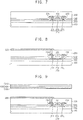
- FIG. 2 is a graph showing peak wavelengths of optical resonances of red light and blue light depending on a thickness of an electron blocking layer.
- a display device (V) including an electron blocking layer having a thickness of about 30nm, a display device (VI) including an electron blocking layer having a thickness of about 50nm, and a display device (VII) including an electron blocking layer having a thickness of about 100nm an optical resonance for red light is generated without causing an optical resonance for blue light. Therefore, purity of colours of light in the display device may be improved by applying the blocking member such as the electron blocking layer.
- the blocking member 440 when the blocking member 440 is disposed between the first organic light emitting layer 430 and the charge generation layer 450 in the first sub-pixel region (I), the blocking member 440 may block the movement of electrons from the charge generation layer 450 to the first organic light emitting layer 430. That is, excitons may not be generated in the first organic light emitting layer 430 in the first sub-pixel region (I) because of the blocking member 440, so that emission of blue light may be prevented or reduced by the blocking member 440.
- substantially only red light may be emitted by the optical resonance in the first sub-pixel region (I), light having a high colour purity may be emitted in the first, the second, and the third sub-pixel regions (I, II, and III), and the display device may ensure high purity of light colours and high brightness without a colour filter.
- a constitution of the display device may be simplified, manufacturing costs thereof may be reduced, and manufacturing processes may be simplified.
- a colour filter is not used over the organic light emitting layers, so that a reduction in the brightness caused by the colour filter may be prevented.
- the display device illustrated in FIG. 3 may have a construction substantially the same as or substantially similar to that of the display device described with reference to FIG. 1 , except for a light emitting structure.
- the display device may include a substrate 100, a switching structure, a first electrode 300, a light emitting structure 402, a second electrode 500, etc.
- a display region of the display device may be divided into first, second, and third sub-pixel regions (I, II, and III), and thus the light emitting structure 402 may be divided into the first, the second, and the third sub-pixel regions (I, II, and III).
- the switching structure including a switching device and at least one or more insulation layers may be disposed on the substrate 100 having a buffer layer 110.
- the switching structure may include a semiconductor layer 210, a gate insulation layer 220, a gate electrode 231, an insulating interlayer 240, a source electrode 233, a drain electrode 235, an insulation layer 250, etc.
- the semiconductor layer 210 may include a first impurity region 211, a channel region 213, and a second impurity region 215.
- a construction of the switching structure may be substantially the same as or substantially similar to that of the switching structure described with reference to FIG. 1 .
- the first electrode 300 may be disposed on the insulation layer 250 in the display region, and a protection layer 280 may be disposed on the insulation layer 250 in a non-display region adjacent to the display region.
- the second electrode 500 may be located above the first electrode 300, and the first and second electrodes 300 and 500 are on opposite sides of the light emitting structure 402.
- An optical distance controlling insulation layer 350 and the light emitting structure 402 may be disposed between the first electrode 300 and the second electrode 500.
- the optical distance controlling insulation layer 350 may be disposed on the first electrode 300 in the display region. In example embodiments, the optical distance controlling insulation layer 350 may be disposed only in the first sub-pixel region (I) and the second sub-pixel region (II). In some example embodiments, the optical distance controlling insulation layer 350 may be positioned in the first sub-pixel region (I), the second sub-pixel region (II), and the third sub-pixel region (III).
- the optical distance controlling insulation layer 350 may have substantially different thicknesses in the first, the second, and the third sub-pixel regions (I, II, and III), and thus gaps (or distances) between the first electrode 300 and the second electrode 500 may be substantially different in the first, the second, and the third sub-pixel regions (I, II, and III), thereby generating optical resonances for different wavelengths of lights with different colours.
- a first hole injection layer 410 of the light emitting structure 402 may be disposed on the first electrode 300 to cover the optical distance controlling insulation layer 350.
- the first hole injection layer 410 may improve a hole injection from the first electrode 300 to a first organic light emitting layer 430.
- the first organic light emitting layer 430 may be disposed on the first hole injection layer 410.
- the first organic light emitting layer 430 may have a single layer structure or a double layer structure.
- the second organic light emitting layer 480 may have the double layer structure including a green light emitting film and a red light emitting film.
- the green light emitting film may include a green dopant dispersed in a host
- the red light emitting layer may include a red dopant dispersed in a host.
- the second organic light emitting layer 480 may have the single layer structure including a green dopant and a red dopant dispersed in a host.
- a charge generation layer 450 may be disposed on the first organic light emitting layer 430.
- the charge generation layer 450 may serve as an anode for the first organic light emitting layer 430, and may serve as a cathode for a second organic light emitting layer 480.
- the charge generation layer 450 may have a single layer structure or a multi-layer structure.
- a second hole injection layer 460 and a hole transfer layer 470 may be located on the charge generation layer 450 to enhance a movement of holes from the charge generation layer 450 to the second organic light emitting layer 480.
- the second organic light emitting layer 480 may be disposed on the hole transfer layer 470.
- the second organic light emitting layer 480 may include a blue light emitting film including a blue dopant dispersed in a host.
- An electron transfer layer 490 may be disposed on the second organic light emitting layer 480 to improve a movement of electrons.
- a blocking member 440 may include an electron blocking layer.
- the electron blocking layer may be disposed between the second organic light emitting layer 480 and the electron transfer layer 490 in the first sub-pixel region (I).
- the blocking member 440 including the electron blocking layer may prevent or reduce the movement of electrons from the electron transfer layer 490 to the second organic light emitting layer 480. Therefore, electrons may not be supplied to the second organic light emitting layer 480 in the first sub-pixel region (I) because of the blocking member 440, so that the second organic light emitting layer 480 in the first sub-pixel region (I) may not emit light.
- the display device with reference to FIG. 3 may include the light emitting structure 402 where the blue light emitting film may change positions with the red and the green light emitting films, and positions of the blocking member 440 and the hole transfer layer 470 may also change. Even though there may be a position change, each optical resonances may be generated in the first, the second, and the third sub-pixel regions (I, II, and III), and emission of blue light may be prevented or reduced by the blocking member 440 in the first sub-pixel region (I), so that the display device may ensure high purity of colours of light, improved colour gamut of light, and high brightness without a colour filter.
- the display device illustrated in FIG. 4 may have a construction substantially the same as or substantially similar to that of the display device described with reference to FIG. 1 , except for a light emitting structure.
- the display device may include a substrate 100, a switching structure, a first electrode 300, a light emitting structure 404, a second electrode 500, etc.
- the display device may include a non-display region and a display region divided into first, second, and third sub-pixel regions (I, II, and III), and thus the light emitting structure 404 in the display region may be divided into the first, the second, and the third sub-pixel regions (I, II, and III).
- a buffer layer 110 may be disposed on the substrate 100, and the switching structure may be disposed on the buffer layer 110.
- the switching structure may include a semiconductor layer 210 (including a first impurity region 211, a channel region 213, and a second impurity region 215), a gate insulation layer 220, a gate electrode 231, an insulating interlayer 240, a source electrode 233, a drain electrode 235, an insulation layer 250, etc.
- a construction of the switching structure has been described in detail with reference to FIG. 1 , so that any further descriptions will be omitted.
- an optical distance controlling insulation layer 350 may be disposed on the first electrode 300. In example embodiments, the optical distance controlling insulation layer 350 may be positioned only in the first sub-pixel region (I) and the second sub-pixel region (II). In some example embodiments, the optical distance controlling insulation layer 350 may be disposed in the first sub-pixel region (I), the second sub-pixel region (II), and the third sub-pixel region (III).
- the optical distance controlling insulation layer 350 may have substantially different thicknesses in the first, the second, and the third sub-pixel regions (I, II, and III), and thus gaps between the first electrode 300 and the second electrode 500 may be substantially different in the first, the second, and the third sub-pixel regions (I, II, and III), thereby generating the optical resonances for different wavelengths of colour lights.
- the light emitting structure 404 in the display region may include a first hole injection layer 410, a hole transfer layer 420, a first organic light emitting layer 430, an additional electron transfer layer 435, a blocking member 440, a charge generation layer 450, a second hole injection layer 460, a second organic light emitting layer 480, an electron transfer layer 490, etc.
- the light emitting structure 404 may have a constitution substantially the same as or substantially similar to that of the light emitting structure 400 described with reference to FIG. 1 .
- the additional electron transfer layer 435 may be disposed between the first organic light emitting layer 430 and the charge generation layer 450.
- the additional electron transfer layer 435 may enhance a movement of electrons from the charge generation layer 450 to the first organic light emitting layer 430, and thus luminance efficiency of the light emitting structure 404 may be improved.
- the blocking member 440 may include an electron blocking layer.
- the electron blocking layer may be disposed on the additional electron transfer layer 435 in the first sub-pixel region (I).
- the blocking member 440 may block the movement of electrons from the charge generation layer 450 to the first organic light emitting layer 430 in the first sub-pixel region (I).
- the electrons may not be supplied to the first organic light emitting layer 430 in the first sub-pixel region (I) because of the blocking member 440, so that the first organic light emitting layer 430 in the first sub-pixel region (I) may not emit light.
- a hole blocking layer (not illustrated) instead of the additional electron transfer layer 435 may be disposed between the first organic light emitting layer 430 and the charge generation layer 450. The hole blocking layer may block a movement of holes from the first organic light emitting layer 430 to the charge generation layer 450, thereby improving the luminance efficiency of the light emitting structure 404.
- the display device with reference to FIG. 4 includes the light emitting structure 404 where the blocking member 440 may be separated from the first organic light emitting layer 430 including the blue light-emitting film. Even though there may be a position change, a movement of electrons to the blue light-emitting film may be blocked or reduced by the blocking member 440, so that substantially only red light may be emitted in the first sub-pixel region (I). Therefore, the display device may ensure high purity of colours of light, improved colour gamut of light, and high brightness without a colour filter.
- the display device illustrated in FIG. 5 may have a construction substantially the same as or substantially similar to that of the display device described with reference to FIG. 1 , except for a light emitting structure.
- the display device may include a substrate 100, a switching structure, a first electrode 300, a light emitting structure 406, a second electrode 500, etc.
- the display device and the light emitting structure 406 may include first, second, and third sub-pixel regions (I, II, and III).
- the switching structure may include one or more insulation layers and a switching device.
- the switching structure may include a semiconductor layer 210 (having a channel region 213, a first impurity region 211, and a second impurity region 215), a gate insulation layer 220, a gate electrode 231, a source electrode 233, a drain electrode 235, etc.
- the one or more insulation layers may include an insulating interlayer 240, an insulation layer 250, etc.
- an optical distance controlling insulation layer 350 may be disposed on the first electrode 300 in a display region of the display device.
- the optical distance controlling insulation layer 350 may be disposed in the first sub-pixel region (I), the second sub-pixel region (II), and/or the third sub-pixel region (III).
- the optical distance controlling insulation layer 350 may have substantially different thicknesses in the first, the second, and the third sub-pixel regions (I, II, and III). Therefore, first, second, and third optical resonance distances may be provided between the first electrode 300 and the second electrode 500 in the first, the second, and the third sub-pixel regions (I, II, and III), respectively.
- the light emitting structure 406 may include a first hole injection layer 410, a hole transfer layer 420, a blocking member 425, a first organic light emitting layer 430, a charge generation layer 450, a second hole injection layer 460, a second organic light emitting layer 480, an electron transfer layer 490, etc.
- the blocking member 425 including an exciton quenching layer (EQL) may be disposed between the first organic light emitting layer 430 and the hole transfer layer 420 in the first sub-pixel region of the light emitting structure 406.
- the exciton quenching layer of the blocking member 425 may include fullerene, a polymer including substituted triarylamine, a carbazole based polymer, 1,1-Bis(4-(N,N-di-p-tolylamino)phenyl)cyclohexane (TAPC), I,I-Bis(4-(N,N-di-p-tolylamino)phenyl)cyclopentane, 4,4'-(9H-fluoren-9-ylidene)bis[N,N-bis(4-methylphenyl)-benzenamine, 1,1-Bis(4-(N,N-di-p-tolylamino)phenyl)-4-phenylcyclohexane, 1,1-Bis(4-(N,N-di-p-tolylamino)phenyl)-4-methylcyclohexane, 1,1-Bis(4-(N,N-di-p-tolylamin
- electrons and holes may collide with each other between the first organic light emitting layer 430 and the hole transfer layer 420 to generate excitons.
- the blocking member 425 including the exciton quenching layer may transform high energy electrons or excitons near the exciton quenching layer to low energy electrons or excitons. Therefore, the electrons or the excitons which may participate in the light emitting process may not exist, so that the first organic light emitting layer 430 may not emit light.
- the display device with reference to FIG. 5 may include the blocking member 425 having the exciton quenching layer instead of an electron blocking layer in the first sub-pixel region. Even though there may be a position change, substantially only red light may be emitted in the first sub-pixel region (I), and emission of blue light may be prevented or reduced.
- the display device illustrated in FIG. 6 may have a construction substantially the same as or substantially similar to that of the display device described with reference to FIG. 1 except for a first electrode 300, a second electrode 500, and an emission type.
- the display device may include a substrate 100, a switching structure, the first electrode 300, a light emitting structure 408, the second electrode 500, etc.
- the switching structure may be disposed on the substrate 100 having a buffer layer 110.
- the switching structure may include a switching device and one or more insulation layers.
- the switching device may include a semiconductor layer 210, a gate insulation layer 220, a gate electrode 231, a source electrode 233, a drain electrode 235, etc.
- the one or more insulation layers may include an insulating interlayer 240, an insulation layer 250, etc.
- the first electrode 300 may serve as a transflective electrode having a reflectivity of about 30% to about 70% with respect to an incident light
- the second electrode 500 may serve as a reflective electrode having a reflectivity of about 70% to about 100% relative to an incident light.
- the first electrode 300 may include a metal, an alloy, a conductive metal oxide, a transparent inorganic material doped with impurities, etc.
- the first electrode 300 may have a multi-layer structure including a plurality of the transparent films or a plurality of the transflective films having different reflective indices.
- the first electrode 300 may have a triple layer structure including a first electrode film, a second electrode film, and a third electrode film.
- the first electrode film and the third electrode film may include a metal oxide containing an indium tin oxide, an indium zinc oxide, a zinc oxide, etc.
- the second electrode film may include a magnesium-silver alloy, silver, a silver-palladium-copper alloy, etc. Even though the second electrode film may include a metal having a relatively high reflectivity, the second electrode film may have a relatively thin thickness, thereby serving as a transflective electrode.
- the second electrode 500 may include aluminum, platinum, silver, gold, chromium, tungsten, molybdenum, titanium, palladium, and alloys of these metals (e.g., Ag-Cu-Au (ACA) alloy or Ag-Pd-Cu (APC) alloy), etc. These materials may be used alone or in a combination thereof.
- ACA Ag-Cu-Au
- APC Ag-Pd-Cu
- a light generated in the light emitting structure 408 may pass through the first electrode 300 and the substrate 100, such that the display device is a bottom emission type.
- an optical distance controlling insulation layer 350 may be disposed on the first electrode 300 in the first sub-pixel region (I), the second sub-pixel region (II), and/or the third sub-pixel region (III).
- the optical distance controlling insulation layer 350 may have substantially different thicknesses in the first, the second, and the third sub-pixel regions (I, II, and III). Therefore, first, second, and third optical resonance distances may be formed between the first electrode 300 and the second electrode 500 in the first, the second, and the third sub-pixel regions (I, II, and III), respectively.
- the light emitting structure 408 of the display device may include a first hole injection layer 410, a hole transfer layer 420, a first organic light emitting layer 430, a blocking member 440, a charge generation layer 450, a second hole injection layer 460, a second organic light emitting layer 480, an electron transfer layer 490, etc.
- the light emitting structure 408 may have a constitution substantially the same as or substantially similar to that of the light emitting structure 400 described with reference to FIG. 1 .
- the blocking member 440 may include an electron blocking layer.
- the electron blocking layer may be disposed between the charge generation layer 450 and the first organic light emitting layer 430 in the first sub-pixel region (I).
- the blocking member 440 may block a movement of electrons from the charge generation layer 450 to the first organic light emitting layer 430 in the first sub-pixel region (I).
- the electrons may not be supplied to the first organic light emitting layer 430 in the first sub-pixel region (I) because of the blocking member 440, so that the first organic light emitting layer 430 in the first sub-pixel region (I) may not emit light.
- the display device with reference to FIG. 6 may be changed into a bottom emission type depending on a material change of the first electrode 300 and the second electrode 500. Even though there may be a position change of the first electrode 300 and the second electrode 500, first, second, and third optical resonances may be generated in the first, the second, and the third sub-pixel regions (I, II, and III), and emission of blue light may be prevented or reduced by the blocking member 440 in the first sub-pixel region so that the display device may ensure high purity of colours of light, improved colour gamut of light, and high brightness without a colour filter.
- FIGS. 7 to 14 are cross-sectional views illustrating a method of manufacturing a display device having a light emitting structure in accordance with example embodiments.
- the display device obtained by the method illustrated in FIGS. 7 to 14 may have a construction substantially the same as or substantially similar to that of the display device described with reference to FIG. 1 .
- the method according to example embodiments may be properly and easily modified to manufacture one of the liquid crystal display devices described with reference to FIGS. 3 to 6 .
- a buffer layer 110 may be formed on a substrate 100.
- the substrate 100 may be formed using a transparent insulation material.
- the buffer layer 110 may be formed using an oxide, a nitride, an oxynitride, an organic insulation material, etc. These may be used alone or in a combination thereof.
- the buffer layer 110 may be formed on the substrate 100 by a chemical vapor deposition (CVD) process, a plasma enhanced chemical vapor deposition (PECVD) process, a high density plasma-chemical vapor deposition (HDP-CVD) process, a spin coating process, a thermal oxidation process, a printing process, etc.
- CVD chemical vapor deposition
- PECVD plasma enhanced chemical vapor deposition
- HDP-CVD high density plasma-chemical vapor deposition
- a switching structure may be formed on the buffer layer 110.
- a gate insulation layer 220 may be formed on the buffer layer 110 to cover the semiconductor layer 210.
- the semiconductor layer 210 may be formed using silicon by a chemical vapor deposition process, a plasma enhanced chemical vapor deposition process, a high density plasma chemical vapor deposition process, a spin coating process, a thermal oxidation process, a printing process, etc.
- the gate insulation layer 220 may be formed using an oxide, an organic insulation material, etc. In this case, the gate insulation layer 220 may be conformally formed along a profile of the semiconductor layer 210.
- the gate insulation layer 220 may be formed by a sputtering process, a chemical vapor deposition process, an atomic layer deposition process, a high density plasma-chemical vapor deposition process, a spin coating process, a printing process, etc.
- a gate electrode 231 may be formed on the gate insulation layer 220 under which the semiconductor layer 210 may be located.
- the gate electrode 231 may be formed using a metal, a metal nitride, a conductive metal oxide, a transparent conductive material, etc. Further, the gate electrode 231 may be formed by a sputtering process, a chemical vapor deposition process, an atomic layer deposition (ALD) process, a spin coating process, a vacuum evaporation process, a pulsed laser deposition (PLD) process, a printing process, etc.
- ALD atomic layer deposition
- PLD pulsed laser deposition
- Impurities may be doped into the semiconductor layer 210 using the gate electrode 220 as an implantation mask, so that a first impurity region 211 and a second impurity region 215 may be formed at lateral portions of the semiconductor layer 210, respectively. Therefore, a central portion of the semiconductor layer 210 may be defined as a channel region 213.
- the first and the second impurity regions 211 and 215 may be formed by an ion implantation process.
- a gate line (not illustrated) may be formed on the gate insulation layer 220. The gate line may extend on the gate insulation layer 220 to contact the gate electrode 231.
- An insulating interlayer 240 may be formed on the gate insulation layer 220 to cover the gate electrode 231.
- the insulating interlayer 240 may be formed using an oxide, a nitride, an oxynitride, an organic insulation material, etc.
- the insulating interlayer 240 may be formed by a sputtering process, a chemical vapor deposition process, a plasma enhanced chemical vapor deposition process, an atomic layer deposition process, a spin coating process, a vapor deposition process, a pulsed laser deposition process, a printing process, etc.
- a source electrode 233 and a drain electrode 235 may be connected to the first impurity region 211 and the second impurity region 215, respectively.
- a data line (not illustrated) may be formed on the insulating interlayer 240.
- the data line may be formed together with the source electrode 233 and the drain electrode 235.
- the data line may extend on the insulating interlayer 240 to contact the source electrode 233.
- the switching device may have a top gate structure in which the gate electrode 231 is disposed over the semiconductor layer 210, however, the scope of example embodiments of the present invention is not limited to such a structure.
- the switching device may have a bottom gate structure including a gate electrode located below a semiconductor layer or an oxide semiconductor device including a semiconductor oxide layer serving as an active layer.
- an insulation layer 250 may be formed on the substrate 100 to cover the switching device, so that the switching structure including the switching device and the insulation layer 250 may be formed on the substrate 100.
- the insulation layer 250 may be formed using a transparent insulation material such as a transparent plastic, a transparent resin, etc. Further, the insulation layer 250 may be formed by a spin coating process, a printing process, a vacuum evaporation process, etc. In example embodiments, an upper portion of the insulation layer 250 may be partially removed by a planarization process such as a chemical mechanical polishing process and/or an etch-back process. In some example embodiments, the insulation layer 250 may be formed using a material having a self planarizing property, and thus the insulation layer 250 may have a substantially flat upper face or surface.
- the insulation layer 250 may be partially removed to form a hole (not illustrated) that may partially expose the drain electrode 235.
- the hole through the insulation layer 250 may be obtained by a photolithography process.
- the first conductive layer may be patterned to form the first electrode 300. Therefore, the first electrode 300 may be directly connected to the drain electrode 235 exposed by the hole.
- the first conductive layer may be formed on the insulation layer 250 by a sputtering process, a printing process, a spray process, a chemical vapor deposition process, an atomic layer deposition process, a vacuum evaporation process, a pulsed laser deposition process, etc.
- the first electrode 300 may be formed using a metal, an alloy, a transparent conductive material, etc.
- the first electrode 300 may serve as a reflective electrode, a transparent electrode, a transflective electrode depending on the materials.
- the first electrode 300 may be formed on the insulation layer 250 and on the contact, the pad, or the plug. In this case, the first electrode 300 may be electrically connected to the drain electrode 235 through the contact, the pad, or the plug.
- an optical distance controlling insulation layer 350 may be formed on the first electrode 300 by a laser induced thermal imaging process.
- the optical distance controlling insulation layer 350 (see FIG. 13 ) may be formed in the second sub-pixel region (II).
- a donor substrate 600 may be disposed above the substrate 100 having the first electrode 300. In this case, after the substrate 100 having the first electrode 300 is fixed using a supporting member (not illustrated), the donor substrate 600 may be aligned with respect to the substrate 100.
- the donor substrate 600 may include a plurality of layers disposed on a base substrate 610.
- the donor substrate 600 may include a light-to-heat conversion (LTHC) layer 620 disposed on the base substrate 610 and a transfer layer 630 located on the light-to-heat conversion layer 620.
- the transfer layer 630 of the donor substrate 600 may be used to form the optical distance controlling insulation layer 350.
- the transfer layer 630 may be formed using a benzocyclobutene-based resin, an olefin-based resin, a polyimide-based resin, an acryl-based resin, a polyvinyl-based resin, a siloxane-based resin, etc. These may be used alone or in a combination thereof.
- the transfer layer 630 may be laminated on the first electrode 300 and the insulation layer 250 by contacting the donor substrate 600 with the substrate 100 and pressurizing the donor substrate 600 using a pressurizing member 640.
- the pressurizing member 640 may include a roller, a crown press, etc.
- the donor substrate 600 may be pressurized using gases without an additional pressurizing member, so that the transfer layer 630 may be laminated on the first electrode 300 and the insulation layer 250.
- a laser irradiation apparatus irradiates a laser beam (indicated using arrows) to the donor substrate 600 in the second sub-pixel region (II).
- the light-to-heat conversion layer 620 converts energy of the laser beam to thermal energy. Therefore, in the second sub-pixel region (II), adhesive strength between the transfer layer 630 and the first electrode 300 may be substantially larger than that between the transfer layer 630 and the light-to-heat conversion layer 620 because of the thermal energy.
- a high resolution pattern may be obtained with a relatively low cost compared to a conventional thin film formation process using a mask.
- the donor substrate 600 is removed from the substrate 100 to form the optical distance controlling insulation layer 350 in the second sub-pixel region (II).
- the donor substrate 600 may be removed by arranging an air blowing apparatus (not illustrated) adjacent to the donor substrate 600, and blowing gases to an edge portion of the donor substrate 600.
- the optical distance controlling insulation layer 350 may be formed on the first electrode 300 in the first sub-pixel region (I) (see FIG. 13 ) by a laser induced thermal imaging process that is substantially the same as or substantially similar to the laser induced thermal imaging process described with reference to FIGS. 10 to 12 .
- a thickness of the optical distance controlling insulation layer 350 may vary depending on a thickness of the transfer layer 630 of the donor substrate 600. Therefore, the optical distance controlling insulation layer 350 may have substantially different thicknesses in the first sub-pixel region (I) and the second sub-pixel region (II).
- the optical distance controlling insulation layer 350 may be formed on the first electrode in the third sub-pixel region (III) (see FIG. 13 ) by a laser induced thermal imaging process that is substantially the same as or substantially similar to the laser induced thermal imaging process described with reference to FIGS. 10 to 12 .
- a protection layer 280 may be formed on the insulation layer 250 in the non-display region of the display device.
- the protection layer 280 may extend on a portion of the first electrode 300 in the display region of the display device.
- the protection layer 280 may be formed using an oxide, a nitride, an oxynitride, an organic insulation material, etc.
- the protection layer 280 may be formed by a chemical vapor deposition process, a spin coating process, a plasma enhanced chemical vapor deposition process, a vacuum evaporation process, a printing process, etc.
- a light emitting structure 400 may be formed on the substrate 100 having the optical distance controlling insulation layer 350 and the protection layer 280.
- the light emitting structure 400 may be formed by sequentially forming a first hole injection layer 410, a hole transfer layer 420, a first organic light emitting layer 430, a blocking member 440, a charge generation layer 450, a second hole injection layer 460, a second organic light emitting layer 480, and an electrode transfer layer 490 on the optical distance controlling insulation layer 350, the first electrode 300, and the protection layer 280.
- the first organic light emitting layer 430 and the second organic light emitting layer 480 may be formed only in the display region, and the blocking member 440 may be formed on the first organic light emitting layer 430 in the first sub-pixel region (I).
- the first hole injection layer 410, the hole transfer layer 420, the first organic light emitting layer 430, the second hole injection layer 460, the second organic light emitting layer 480, and the electron transfer layer 490 including an organic material may be formed by a vacuum evaporation process, a printing process, a spin coating process, a laser induced thermal imaging process, etc.
- the charge generation layer 450 including a metal and/or a metal oxide may be formed by a sputtering process, a printing process, a spray process, a chemical vapor deposition process, etc.
- the blocking member 440 including an electron blocking layer or an exciton quenching layer may be formed on the first organic light emitting layer 430 by a laser induced thermal imaging process that is substantially the same as or substantially similar to the laser induced thermal imaging process described with reference to FIGS. 10 to 12 .
- a second electrode 500 may be formed on the electron transfer layer 490.
- the second electrode 500 may be formed using a metal, an alloy, and/or a transparent conductive material by a sputtering process, a printing process, a spray process, a chemical vapor deposition process, a vacuum evaporation process, an atomic layer deposition process, etc.
- a display device having a light emitting structure may ensure an improved purity of colours of light without a colour filter, a manufacturing cost of the display device may be reduced, and manufacturing processes of the display device may be simplified.
- the display device having various emission types such as a bottom emission type, a top emission type, or a dual emission type may be employed in various electronic and electric apparatuses such as televisions, mobile communication apparatuses, monitors, MP3 players, portable display apparatuses, etc.
Landscapes
- Physics & Mathematics (AREA)
- Optics & Photonics (AREA)
- Engineering & Computer Science (AREA)
- Manufacturing & Machinery (AREA)
- Microelectronics & Electronic Packaging (AREA)
- Electroluminescent Light Sources (AREA)
- Devices For Indicating Variable Information By Combining Individual Elements (AREA)
Applications Claiming Priority (1)
| Application Number | Priority Date | Filing Date | Title |
|---|---|---|---|
| KR1020110063644A KR101884199B1 (ko) | 2011-06-29 | 2011-06-29 | 발광 구조물, 발광 구조물을 포함하는 표시 장치 및 표시 장치의 제조 방법 |
Publications (2)
| Publication Number | Publication Date |
|---|---|
| EP2541602A1 true EP2541602A1 (de) | 2013-01-02 |
| EP2541602B1 EP2541602B1 (de) | 2018-01-24 |
Family
ID=45656542
Family Applications (1)
| Application Number | Title | Priority Date | Filing Date |
|---|---|---|---|
| EP12156715.0A Active EP2541602B1 (de) | 2011-06-29 | 2012-02-23 | Lichtemittierende Struktur, Anzeigevorrichtung und Herstellungsverfahren |
Country Status (6)
| Country | Link |
|---|---|
| US (3) | US9172058B2 (de) |
| EP (1) | EP2541602B1 (de) |
| JP (1) | JP6073056B2 (de) |
| KR (1) | KR101884199B1 (de) |
| CN (1) | CN102856507B (de) |
| TW (1) | TWI605624B (de) |
Cited By (2)
| Publication number | Priority date | Publication date | Assignee | Title |
|---|---|---|---|---|
| US10504966B2 (en) | 2014-05-15 | 2019-12-10 | Semiconductor Energy Laboratory Co., Ltd. | Light-emitting device comprising transparent conductive films having different thicknesses |
| US20220236462A1 (en) * | 2021-01-26 | 2022-07-28 | Ron Varghese | Planarized patterned optical thin film coatings |
Families Citing this family (29)
| Publication number | Priority date | Publication date | Assignee | Title |
|---|---|---|---|---|
| KR102109166B1 (ko) | 2013-01-15 | 2020-05-12 | 삼성디스플레이 주식회사 | 박막 트랜지스터 및 이를 구비하는 표시 기판 |
| KR102081209B1 (ko) * | 2013-03-26 | 2020-02-26 | 삼성디스플레이 주식회사 | 유기 발광 표시 장치 및 그 제조 방법, 및 그 유기 발광 표시 장치의 제조에 사용되는 도너 기판 및 도너 기판 세트 |
| JP6286941B2 (ja) * | 2013-08-27 | 2018-03-07 | セイコーエプソン株式会社 | 発光装置、発光装置の製造方法、電子機器 |
| CN103824875B (zh) | 2013-12-10 | 2015-07-08 | 京东方科技集团股份有限公司 | Oled显示面板及其制作方法、显示装置 |
| CN103779387B (zh) * | 2014-01-06 | 2018-11-02 | 京东方科技集团股份有限公司 | Oled显示面板及显示装置 |
| CN104851980B (zh) * | 2014-02-13 | 2017-02-08 | 上海和辉光电有限公司 | 全彩有机发光二极管结构 |
| US20160093272A1 (en) * | 2014-09-29 | 2016-03-31 | Brother Kogyo Kabushiki Kaisha | Information processing device and non-transitory storage medium storing instructions executable by the information processing device |
| KR102299838B1 (ko) | 2014-10-31 | 2021-09-07 | 엘지디스플레이 주식회사 | 유기 발광 소자 및 그의 제조 방법 |
| WO2016149673A1 (en) * | 2015-03-18 | 2016-09-22 | University Of Pittsburgh - Of The Commonwealth System Of Higher Education | Bioactive components conjugated to substrates of microneedle arrays |
| CN104733506B (zh) * | 2015-04-01 | 2017-10-24 | 京东方科技集团股份有限公司 | 一种电致发光显示器件及显示装置 |
| KR20170001827A (ko) * | 2015-06-25 | 2017-01-05 | 삼성디스플레이 주식회사 | 유기 발광 표시 장치 |
| JP2017062884A (ja) * | 2015-09-24 | 2017-03-30 | ソニー株式会社 | 表示装置及び発光装置 |
| KR102406606B1 (ko) * | 2015-10-08 | 2022-06-09 | 삼성디스플레이 주식회사 | 유기 발광 소자, 이를 포함하는 유기 발광 표시 장치, 및 이의 제조 방법 |
| WO2017187571A1 (ja) * | 2016-04-27 | 2017-11-02 | ギガフォトン株式会社 | 極端紫外光センサユニット及び極端紫外光生成装置 |
| CN105895819B (zh) * | 2016-04-28 | 2018-07-06 | 京东方科技集团股份有限公司 | 一种oled器件及其制备方法、oled显示面板 |
| KR102521254B1 (ko) * | 2016-06-01 | 2023-04-17 | 삼성디스플레이 주식회사 | 표시 패널 및 이의 제조 방법 |
| JP7126823B2 (ja) * | 2016-12-23 | 2022-08-29 | 株式会社半導体エネルギー研究所 | 半導体装置の作製方法 |
| KR102354977B1 (ko) | 2017-07-03 | 2022-01-25 | 삼성디스플레이 주식회사 | 디스플레이 장치 |
| CN109841643B (zh) * | 2017-11-24 | 2021-12-03 | 比亚迪半导体股份有限公司 | 一种白光led芯片结构及制作方法 |
| JP2019192448A (ja) * | 2018-04-24 | 2019-10-31 | 株式会社ジャパンディスプレイ | 表示装置 |
| KR102679757B1 (ko) * | 2018-12-13 | 2024-06-28 | 엘지디스플레이 주식회사 | 전계 발광 표시 장치 |
| KR102735978B1 (ko) * | 2018-12-21 | 2024-11-28 | 엘지디스플레이 주식회사 | 표시장치 |
| KR102690482B1 (ko) * | 2018-12-28 | 2024-07-31 | 엘지디스플레이 주식회사 | 발광 표시 장치 및 이의 제조 방법 |
| KR102661468B1 (ko) * | 2019-02-15 | 2024-04-30 | 삼성디스플레이 주식회사 | 유기 발광 소자 및 이를 포함한 전자 장치 |
| KR102565182B1 (ko) * | 2019-09-30 | 2023-08-08 | 엘지디스플레이 주식회사 | 전계 발광 표시 장치 |
| KR102687966B1 (ko) * | 2019-12-30 | 2024-07-23 | 엘지디스플레이 주식회사 | 표시장치 |
| US11646300B2 (en) * | 2020-09-01 | 2023-05-09 | Jade Bird Display (shanghai) Limited | Double color micro LED display panel |
| CN112786764B (zh) * | 2021-02-26 | 2022-02-22 | 维沃移动通信有限公司 | 发光器件、显示组件和发光器件的制造方法 |
| TWI867912B (zh) * | 2023-12-25 | 2024-12-21 | 瀚宇彩晶股份有限公司 | 畫素陣列基板及顯示裝置 |
Citations (4)
| Publication number | Priority date | Publication date | Assignee | Title |
|---|---|---|---|---|
| WO2004061878A2 (en) * | 2002-12-31 | 2004-07-22 | Eastman Kodak Company | Using hole- or electron-blocking layers in color oleds |
| US20060232202A1 (en) * | 2005-04-15 | 2006-10-19 | Eisuke Matsuda | Display device and a method of manufacturing the display device |
| US20090051275A1 (en) * | 2007-08-21 | 2009-02-26 | Seiko Epson Corporation | Light emitting device |
| US20110073885A1 (en) * | 2009-09-25 | 2011-03-31 | Chang-Oh Kim | Organic electroluminescent device |
Family Cites Families (17)
| Publication number | Priority date | Publication date | Assignee | Title |
|---|---|---|---|---|
| JP3758694B2 (ja) * | 1994-10-13 | 2006-03-22 | 三星エスディアイ株式会社 | 有機薄膜el素子 |
| TW495809B (en) * | 2000-02-28 | 2002-07-21 | Semiconductor Energy Lab | Thin film forming device, thin film forming method, and self-light emitting device |
| JP2002208483A (ja) * | 2001-01-11 | 2002-07-26 | Sharp Corp | 有機エレクトロルミネッセンス素子およびその製造方法 |
| JP4644938B2 (ja) * | 2001-01-15 | 2011-03-09 | ソニー株式会社 | 有機電界発光素子 |
| US7158161B2 (en) * | 2002-09-20 | 2007-01-02 | Matsushita Electric Industrial Co., Ltd. | Organic electroluminescence element and an exposure unit and image-forming apparatus both using the element |
| KR100721554B1 (ko) * | 2004-07-22 | 2007-05-23 | 삼성에스디아이 주식회사 | 유기 전계 발광 소자 및 그의 제조 방법 |
| JP4797438B2 (ja) * | 2005-05-17 | 2011-10-19 | ソニー株式会社 | 有機電界発光素子および表示装置 |
| US7888860B2 (en) | 2006-08-25 | 2011-02-15 | Samsung Electronics Co., Ltd. | Organic light emitting device |
| KR20080018557A (ko) | 2006-08-25 | 2008-02-28 | 삼성전자주식회사 | 유기 발광 장치 |
| KR100829761B1 (ko) * | 2007-05-16 | 2008-05-15 | 삼성에스디아이 주식회사 | 유기 발광 소자 |
| KR101407580B1 (ko) | 2007-09-17 | 2014-06-13 | 삼성디스플레이 주식회사 | 백색 유기발광소자 및 그를 포함하는 표시장치와 조명장치 |
| JP2010056016A (ja) | 2008-08-29 | 2010-03-11 | Fujifilm Corp | カラー表示装置及びその製造方法 |
| JP4775865B2 (ja) * | 2009-01-14 | 2011-09-21 | 東芝モバイルディスプレイ株式会社 | 有機el表示装置及びその製造方法 |
| JP5502092B2 (ja) * | 2009-09-15 | 2014-05-28 | シャープ株式会社 | 蒸着方法および蒸着装置 |
| KR101058109B1 (ko) * | 2009-09-15 | 2011-08-24 | 삼성모바일디스플레이주식회사 | 유기 발광 디스플레이 장치 |
| US8466455B2 (en) * | 2009-09-17 | 2013-06-18 | Universal Display Corporation | Device structure |
| CN101710608B (zh) * | 2009-12-01 | 2012-08-08 | 中山大学 | 一种顶发射有机白光器件 |
-
2011
- 2011-06-29 KR KR1020110063644A patent/KR101884199B1/ko active Active
- 2011-11-15 JP JP2011249766A patent/JP6073056B2/ja active Active
- 2011-11-17 US US13/299,311 patent/US9172058B2/en active Active
- 2011-12-05 TW TW100144597A patent/TWI605624B/zh active
-
2012
- 2012-02-23 EP EP12156715.0A patent/EP2541602B1/de active Active
- 2012-03-09 CN CN201210061071.3A patent/CN102856507B/zh active Active
-
2015
- 2015-09-18 US US14/859,156 patent/US9947903B2/en active Active
-
2018
- 2018-04-13 US US15/953,342 patent/US10312477B2/en active Active
Patent Citations (4)
| Publication number | Priority date | Publication date | Assignee | Title |
|---|---|---|---|---|
| WO2004061878A2 (en) * | 2002-12-31 | 2004-07-22 | Eastman Kodak Company | Using hole- or electron-blocking layers in color oleds |
| US20060232202A1 (en) * | 2005-04-15 | 2006-10-19 | Eisuke Matsuda | Display device and a method of manufacturing the display device |
| US20090051275A1 (en) * | 2007-08-21 | 2009-02-26 | Seiko Epson Corporation | Light emitting device |
| US20110073885A1 (en) * | 2009-09-25 | 2011-03-31 | Chang-Oh Kim | Organic electroluminescent device |
Cited By (3)
| Publication number | Priority date | Publication date | Assignee | Title |
|---|---|---|---|---|
| US10504966B2 (en) | 2014-05-15 | 2019-12-10 | Semiconductor Energy Laboratory Co., Ltd. | Light-emitting device comprising transparent conductive films having different thicknesses |
| US20220236462A1 (en) * | 2021-01-26 | 2022-07-28 | Ron Varghese | Planarized patterned optical thin film coatings |
| US12276818B2 (en) * | 2021-01-26 | 2025-04-15 | Ron Varghese | Planarized patterned optical thin film coatings |
Also Published As
| Publication number | Publication date |
|---|---|
| US9172058B2 (en) | 2015-10-27 |
| JP2013012456A (ja) | 2013-01-17 |
| CN102856507A (zh) | 2013-01-02 |
| KR20130007692A (ko) | 2013-01-21 |
| KR101884199B1 (ko) | 2018-08-02 |
| CN102856507B (zh) | 2016-12-14 |
| US10312477B2 (en) | 2019-06-04 |
| EP2541602B1 (de) | 2018-01-24 |
| TWI605624B (zh) | 2017-11-11 |
| TW201301599A (zh) | 2013-01-01 |
| US20130001612A1 (en) | 2013-01-03 |
| US9947903B2 (en) | 2018-04-17 |
| US20180241010A1 (en) | 2018-08-23 |
| US20160013454A1 (en) | 2016-01-14 |
| JP6073056B2 (ja) | 2017-02-01 |
Similar Documents
| Publication | Publication Date | Title |
|---|---|---|
| US10312477B2 (en) | Light emitting structure, display device including a light emitting structure and method of manufacturing a display device including a light emitting structure | |
| US11380734B2 (en) | Organic light emitting diode display including capping layer having optical thickness for improving optics | |
| CN112071996B (zh) | 有机发光装置及使用该有机发光装置的有机发光显示装置 | |
| US9425422B2 (en) | Organic light emitting display device | |
| JP5094477B2 (ja) | 有機発光表示装置及びその製造方法 | |
| EP3188272A1 (de) | Blaue organische lichtemittierende vorrichtung und anzeigevorrichtung damit | |
| US10381600B2 (en) | Organic electroluminescence device, illumination device, and display device | |
| US10020348B2 (en) | Organic light emitting display device with multiple emission layers | |
| CN103915577A (zh) | 有机发光显示器件及其制造方法 | |
| US10826021B2 (en) | Organic electroluminescence device including a plurality of unit regions each including a light emitting area and a transmissive area | |
| JP2016164855A (ja) | 発光装置並びにこれを備えた表示装置、照明装置および電子機器 | |
| US10032830B2 (en) | Organic light emitting display device | |
| US20120098412A1 (en) | Display devices and methods of manufacturing display devices | |
| KR102113609B1 (ko) | 유기 발광 표시 장치 및 그의 제조 방법 | |
| KR20220163324A (ko) | 백색 유기 발광 소자 | |
| US10249849B2 (en) | Organic light emitting display device | |
| KR102410031B1 (ko) | 유기 발광 소자, 그의 제조방법, 및 유기 발광 소자를 구비한 유기 발광 표시장치 | |
| KR102108174B1 (ko) | 유기 발광 구조물의 제조 방법 및 유기 발광 표시 장치의 제조 방법 |
Legal Events
| Date | Code | Title | Description |
|---|---|---|---|
| PUAI | Public reference made under article 153(3) epc to a published international application that has entered the european phase |
Free format text: ORIGINAL CODE: 0009012 |
|
| AK | Designated contracting states |
Kind code of ref document: A1 Designated state(s): AL AT BE BG CH CY CZ DE DK EE ES FI FR GB GR HR HU IE IS IT LI LT LU LV MC MK MT NL NO PL PT RO RS SE SI SK SM TR |
|
| AX | Request for extension of the european patent |
Extension state: BA ME |
|
| 17P | Request for examination filed |
Effective date: 20130614 |
|
| RBV | Designated contracting states (corrected) |
Designated state(s): AL AT BE BG CH CY CZ DE DK EE ES FI FR GB GR HR HU IE IS IT LI LT LU LV MC MK MT NL NO PL PT RO RS SE SI SK SM TR |
|
| RAP1 | Party data changed (applicant data changed or rights of an application transferred) |
Owner name: SAMSUNG DISPLAY CO., LTD. |
|
| STAA | Information on the status of an ep patent application or granted ep patent |
Free format text: STATUS: EXAMINATION IS IN PROGRESS |
|
| 17Q | First examination report despatched |
Effective date: 20170113 |
|
| GRAP | Despatch of communication of intention to grant a patent |
Free format text: ORIGINAL CODE: EPIDOSNIGR1 |
|
| STAA | Information on the status of an ep patent application or granted ep patent |
Free format text: STATUS: GRANT OF PATENT IS INTENDED |
|
| RIC1 | Information provided on ipc code assigned before grant |
Ipc: H01L 27/32 20060101AFI20170705BHEP Ipc: H01L 51/50 20060101ALI20170705BHEP Ipc: H01L 51/52 20060101ALI20170705BHEP |
|
| INTG | Intention to grant announced |
Effective date: 20170721 |
|
| GRAS | Grant fee paid |
Free format text: ORIGINAL CODE: EPIDOSNIGR3 |
|
| GRAA | (expected) grant |
Free format text: ORIGINAL CODE: 0009210 |
|
| STAA | Information on the status of an ep patent application or granted ep patent |
Free format text: STATUS: THE PATENT HAS BEEN GRANTED |
|
| AK | Designated contracting states |
Kind code of ref document: B1 Designated state(s): AL AT BE BG CH CY CZ DE DK EE ES FI FR GB GR HR HU IE IS IT LI LT LU LV MC MK MT NL NO PL PT RO RS SE SI SK SM TR |
|
| REG | Reference to a national code |
Ref country code: GB Ref legal event code: FG4D |
|
| REG | Reference to a national code |
Ref country code: CH Ref legal event code: EP |
|
| REG | Reference to a national code |
Ref country code: AT Ref legal event code: REF Ref document number: 966231 Country of ref document: AT Kind code of ref document: T Effective date: 20180215 |
|
| REG | Reference to a national code |
Ref country code: IE Ref legal event code: FG4D |
|
| REG | Reference to a national code |
Ref country code: FR Ref legal event code: PLFP Year of fee payment: 7 |
|
| REG | Reference to a national code |
Ref country code: DE Ref legal event code: R096 Ref document number: 602012042251 Country of ref document: DE |
|
| REG | Reference to a national code |
Ref country code: NL Ref legal event code: FP |
|
| REG | Reference to a national code |
Ref country code: LT Ref legal event code: MG4D |
|
| REG | Reference to a national code |
Ref country code: AT Ref legal event code: MK05 Ref document number: 966231 Country of ref document: AT Kind code of ref document: T Effective date: 20180124 |
|
| PG25 | Lapsed in a contracting state [announced via postgrant information from national office to epo] |
Ref country code: HR Free format text: LAPSE BECAUSE OF FAILURE TO SUBMIT A TRANSLATION OF THE DESCRIPTION OR TO PAY THE FEE WITHIN THE PRESCRIBED TIME-LIMIT Effective date: 20180124 Ref country code: ES Free format text: LAPSE BECAUSE OF FAILURE TO SUBMIT A TRANSLATION OF THE DESCRIPTION OR TO PAY THE FEE WITHIN THE PRESCRIBED TIME-LIMIT Effective date: 20180124 Ref country code: LT Free format text: LAPSE BECAUSE OF FAILURE TO SUBMIT A TRANSLATION OF THE DESCRIPTION OR TO PAY THE FEE WITHIN THE PRESCRIBED TIME-LIMIT Effective date: 20180124 Ref country code: FI Free format text: LAPSE BECAUSE OF FAILURE TO SUBMIT A TRANSLATION OF THE DESCRIPTION OR TO PAY THE FEE WITHIN THE PRESCRIBED TIME-LIMIT Effective date: 20180124 Ref country code: NO Free format text: LAPSE BECAUSE OF FAILURE TO SUBMIT A TRANSLATION OF THE DESCRIPTION OR TO PAY THE FEE WITHIN THE PRESCRIBED TIME-LIMIT Effective date: 20180424 Ref country code: CY Free format text: LAPSE BECAUSE OF FAILURE TO SUBMIT A TRANSLATION OF THE DESCRIPTION OR TO PAY THE FEE WITHIN THE PRESCRIBED TIME-LIMIT Effective date: 20180124 |
|
| PG25 | Lapsed in a contracting state [announced via postgrant information from national office to epo] |
Ref country code: PL Free format text: LAPSE BECAUSE OF FAILURE TO SUBMIT A TRANSLATION OF THE DESCRIPTION OR TO PAY THE FEE WITHIN THE PRESCRIBED TIME-LIMIT Effective date: 20180124 Ref country code: GR Free format text: LAPSE BECAUSE OF FAILURE TO SUBMIT A TRANSLATION OF THE DESCRIPTION OR TO PAY THE FEE WITHIN THE PRESCRIBED TIME-LIMIT Effective date: 20180425 Ref country code: AT Free format text: LAPSE BECAUSE OF FAILURE TO SUBMIT A TRANSLATION OF THE DESCRIPTION OR TO PAY THE FEE WITHIN THE PRESCRIBED TIME-LIMIT Effective date: 20180124 Ref country code: IS Free format text: LAPSE BECAUSE OF FAILURE TO SUBMIT A TRANSLATION OF THE DESCRIPTION OR TO PAY THE FEE WITHIN THE PRESCRIBED TIME-LIMIT Effective date: 20180524 Ref country code: SE Free format text: LAPSE BECAUSE OF FAILURE TO SUBMIT A TRANSLATION OF THE DESCRIPTION OR TO PAY THE FEE WITHIN THE PRESCRIBED TIME-LIMIT Effective date: 20180124 Ref country code: LV Free format text: LAPSE BECAUSE OF FAILURE TO SUBMIT A TRANSLATION OF THE DESCRIPTION OR TO PAY THE FEE WITHIN THE PRESCRIBED TIME-LIMIT Effective date: 20180124 Ref country code: BG Free format text: LAPSE BECAUSE OF FAILURE TO SUBMIT A TRANSLATION OF THE DESCRIPTION OR TO PAY THE FEE WITHIN THE PRESCRIBED TIME-LIMIT Effective date: 20180424 Ref country code: RS Free format text: LAPSE BECAUSE OF FAILURE TO SUBMIT A TRANSLATION OF THE DESCRIPTION OR TO PAY THE FEE WITHIN THE PRESCRIBED TIME-LIMIT Effective date: 20180124 |
|
| REG | Reference to a national code |
Ref country code: CH Ref legal event code: PL |
|
| REG | Reference to a national code |
Ref country code: DE Ref legal event code: R097 Ref document number: 602012042251 Country of ref document: DE |
|
| PG25 | Lapsed in a contracting state [announced via postgrant information from national office to epo] |
Ref country code: RO Free format text: LAPSE BECAUSE OF FAILURE TO SUBMIT A TRANSLATION OF THE DESCRIPTION OR TO PAY THE FEE WITHIN THE PRESCRIBED TIME-LIMIT Effective date: 20180124 Ref country code: IT Free format text: LAPSE BECAUSE OF FAILURE TO SUBMIT A TRANSLATION OF THE DESCRIPTION OR TO PAY THE FEE WITHIN THE PRESCRIBED TIME-LIMIT Effective date: 20180124 Ref country code: AL Free format text: LAPSE BECAUSE OF FAILURE TO SUBMIT A TRANSLATION OF THE DESCRIPTION OR TO PAY THE FEE WITHIN THE PRESCRIBED TIME-LIMIT Effective date: 20180124 Ref country code: MC Free format text: LAPSE BECAUSE OF FAILURE TO SUBMIT A TRANSLATION OF THE DESCRIPTION OR TO PAY THE FEE WITHIN THE PRESCRIBED TIME-LIMIT Effective date: 20180124 Ref country code: EE Free format text: LAPSE BECAUSE OF FAILURE TO SUBMIT A TRANSLATION OF THE DESCRIPTION OR TO PAY THE FEE WITHIN THE PRESCRIBED TIME-LIMIT Effective date: 20180124 |
|
| REG | Reference to a national code |
Ref country code: BE Ref legal event code: MM Effective date: 20180228 |
|
| PG25 | Lapsed in a contracting state [announced via postgrant information from national office to epo] |
Ref country code: SM Free format text: LAPSE BECAUSE OF FAILURE TO SUBMIT A TRANSLATION OF THE DESCRIPTION OR TO PAY THE FEE WITHIN THE PRESCRIBED TIME-LIMIT Effective date: 20180124 Ref country code: DK Free format text: LAPSE BECAUSE OF FAILURE TO SUBMIT A TRANSLATION OF THE DESCRIPTION OR TO PAY THE FEE WITHIN THE PRESCRIBED TIME-LIMIT Effective date: 20180124 Ref country code: CZ Free format text: LAPSE BECAUSE OF FAILURE TO SUBMIT A TRANSLATION OF THE DESCRIPTION OR TO PAY THE FEE WITHIN THE PRESCRIBED TIME-LIMIT Effective date: 20180124 Ref country code: LU Free format text: LAPSE BECAUSE OF NON-PAYMENT OF DUE FEES Effective date: 20180223 Ref country code: CH Free format text: LAPSE BECAUSE OF NON-PAYMENT OF DUE FEES Effective date: 20180228 Ref country code: LI Free format text: LAPSE BECAUSE OF NON-PAYMENT OF DUE FEES Effective date: 20180228 Ref country code: SK Free format text: LAPSE BECAUSE OF FAILURE TO SUBMIT A TRANSLATION OF THE DESCRIPTION OR TO PAY THE FEE WITHIN THE PRESCRIBED TIME-LIMIT Effective date: 20180124 |
|
| PLBE | No opposition filed within time limit |
Free format text: ORIGINAL CODE: 0009261 |
|
| STAA | Information on the status of an ep patent application or granted ep patent |
Free format text: STATUS: NO OPPOSITION FILED WITHIN TIME LIMIT |
|
| REG | Reference to a national code |
Ref country code: IE Ref legal event code: MM4A |
|
| 26N | No opposition filed |
Effective date: 20181025 |
|
| PG25 | Lapsed in a contracting state [announced via postgrant information from national office to epo] |
Ref country code: IE Free format text: LAPSE BECAUSE OF NON-PAYMENT OF DUE FEES Effective date: 20180223 |
|
| PG25 | Lapsed in a contracting state [announced via postgrant information from national office to epo] |
Ref country code: BE Free format text: LAPSE BECAUSE OF NON-PAYMENT OF DUE FEES Effective date: 20180228 Ref country code: SI Free format text: LAPSE BECAUSE OF FAILURE TO SUBMIT A TRANSLATION OF THE DESCRIPTION OR TO PAY THE FEE WITHIN THE PRESCRIBED TIME-LIMIT Effective date: 20180124 |
|
| PG25 | Lapsed in a contracting state [announced via postgrant information from national office to epo] |
Ref country code: MT Free format text: LAPSE BECAUSE OF NON-PAYMENT OF DUE FEES Effective date: 20180223 |
|
| PG25 | Lapsed in a contracting state [announced via postgrant information from national office to epo] |
Ref country code: TR Free format text: LAPSE BECAUSE OF FAILURE TO SUBMIT A TRANSLATION OF THE DESCRIPTION OR TO PAY THE FEE WITHIN THE PRESCRIBED TIME-LIMIT Effective date: 20180124 |
|
| PG25 | Lapsed in a contracting state [announced via postgrant information from national office to epo] |
Ref country code: HU Free format text: LAPSE BECAUSE OF FAILURE TO SUBMIT A TRANSLATION OF THE DESCRIPTION OR TO PAY THE FEE WITHIN THE PRESCRIBED TIME-LIMIT; INVALID AB INITIO Effective date: 20120223 Ref country code: PT Free format text: LAPSE BECAUSE OF FAILURE TO SUBMIT A TRANSLATION OF THE DESCRIPTION OR TO PAY THE FEE WITHIN THE PRESCRIBED TIME-LIMIT Effective date: 20180124 |
|
| PG25 | Lapsed in a contracting state [announced via postgrant information from national office to epo] |
Ref country code: MK Free format text: LAPSE BECAUSE OF NON-PAYMENT OF DUE FEES Effective date: 20180124 |
|
| REG | Reference to a national code |
Ref country code: DE Ref legal event code: R079 Ref document number: 602012042251 Country of ref document: DE Free format text: PREVIOUS MAIN CLASS: H01L0027320000 Ipc: H10K0059000000 |
|
| P01 | Opt-out of the competence of the unified patent court (upc) registered |
Effective date: 20230515 |
|
| PGFP | Annual fee paid to national office [announced via postgrant information from national office to epo] |
Ref country code: NL Payment date: 20260121 Year of fee payment: 15 |
|
| PGFP | Annual fee paid to national office [announced via postgrant information from national office to epo] |
Ref country code: GB Payment date: 20260122 Year of fee payment: 15 |
|
| PGFP | Annual fee paid to national office [announced via postgrant information from national office to epo] |
Ref country code: DE Payment date: 20260120 Year of fee payment: 15 |
|
| PGFP | Annual fee paid to national office [announced via postgrant information from national office to epo] |
Ref country code: FR Payment date: 20260121 Year of fee payment: 15 |