EP2530726A2 - Empilement de type n multicouche pour dispositifs photovoltaïques à couche mince à base de tellurure de cadmium et procédés de fabrication - Google Patents
Empilement de type n multicouche pour dispositifs photovoltaïques à couche mince à base de tellurure de cadmium et procédés de fabrication Download PDFInfo
- Publication number
- EP2530726A2 EP2530726A2 EP12169573A EP12169573A EP2530726A2 EP 2530726 A2 EP2530726 A2 EP 2530726A2 EP 12169573 A EP12169573 A EP 12169573A EP 12169573 A EP12169573 A EP 12169573A EP 2530726 A2 EP2530726 A2 EP 2530726A2
- Authority
- EP
- European Patent Office
- Prior art keywords
- layer
- cadmium
- target
- sputtering
- type stack
- Prior art date
- Legal status (The legal status is an assumption and is not a legal conclusion. Google has not performed a legal analysis and makes no representation as to the accuracy of the status listed.)
- Withdrawn
Links
- MARUHZGHZWCEQU-UHFFFAOYSA-N 5-phenyl-2h-tetrazole Chemical compound C1=CC=CC=C1C1=NNN=N1 MARUHZGHZWCEQU-UHFFFAOYSA-N 0.000 title claims abstract description 70
- 238000000034 method Methods 0.000 title claims abstract description 22
- 239000010409 thin film Substances 0.000 title claims abstract description 17
- WUPHOULIZUERAE-UHFFFAOYSA-N 3-(oxolan-2-yl)propanoic acid Chemical compound OC(=O)CCC1CCCO1 WUPHOULIZUERAE-UHFFFAOYSA-N 0.000 claims abstract description 54
- 229910052980 cadmium sulfide Inorganic materials 0.000 claims abstract description 53
- 239000011521 glass Substances 0.000 claims abstract description 23
- 239000006096 absorbing agent Substances 0.000 claims abstract description 7
- 238000004544 sputter deposition Methods 0.000 claims description 41
- CXKCTMHTOKXKQT-UHFFFAOYSA-N cadmium oxide Inorganic materials [Cd]=O CXKCTMHTOKXKQT-UHFFFAOYSA-N 0.000 claims description 31
- CFEAAQFZALKQPA-UHFFFAOYSA-N cadmium(2+);oxygen(2-) Chemical compound [O-2].[Cd+2] CFEAAQFZALKQPA-UHFFFAOYSA-N 0.000 claims description 31
- 229910052760 oxygen Inorganic materials 0.000 claims description 24
- 239000001301 oxygen Substances 0.000 claims description 24
- QVGXLLKOCUKJST-UHFFFAOYSA-N atomic oxygen Chemical compound [O] QVGXLLKOCUKJST-UHFFFAOYSA-N 0.000 claims description 23
- 239000000203 mixture Substances 0.000 claims description 20
- 239000000758 substrate Substances 0.000 claims description 17
- 229910052793 cadmium Inorganic materials 0.000 claims description 15
- QCUOBSQYDGUHHT-UHFFFAOYSA-L cadmium sulfate Chemical compound [Cd+2].[O-]S([O-])(=O)=O QCUOBSQYDGUHHT-UHFFFAOYSA-L 0.000 claims description 15
- 229910000331 cadmium sulfate Inorganic materials 0.000 claims description 13
- BYJADUSHMADYRW-UHFFFAOYSA-L cadmium(2+);sulfite Chemical compound [Cd+2].[O-]S([O-])=O BYJADUSHMADYRW-UHFFFAOYSA-L 0.000 claims description 13
- 238000000151 deposition Methods 0.000 claims description 13
- 239000012298 atmosphere Substances 0.000 claims description 12
- BDOSMKKIYDKNTQ-UHFFFAOYSA-N cadmium atom Chemical compound [Cd] BDOSMKKIYDKNTQ-UHFFFAOYSA-N 0.000 claims description 12
- 150000001875 compounds Chemical class 0.000 claims description 12
- NINIDFKCEFEMDL-UHFFFAOYSA-N Sulfur Chemical compound [S] NINIDFKCEFEMDL-UHFFFAOYSA-N 0.000 claims description 11
- 229910052717 sulfur Inorganic materials 0.000 claims description 11
- 239000011593 sulfur Substances 0.000 claims description 11
- BTWVLFJYEVGKNZ-UHFFFAOYSA-N S=O.[Cd] Chemical compound S=O.[Cd] BTWVLFJYEVGKNZ-UHFFFAOYSA-N 0.000 claims 2
- 238000004519 manufacturing process Methods 0.000 abstract description 8
- 239000010410 layer Substances 0.000 description 330
- 239000000463 material Substances 0.000 description 23
- 230000005855 radiation Effects 0.000 description 12
- 229910052751 metal Inorganic materials 0.000 description 11
- 239000002184 metal Substances 0.000 description 11
- XOLBLPGZBRYERU-UHFFFAOYSA-N tin dioxide Chemical compound O=[Sn]=O XOLBLPGZBRYERU-UHFFFAOYSA-N 0.000 description 10
- XLOMVQKBTHCTTD-UHFFFAOYSA-N Zinc monoxide Chemical compound [Zn]=O XLOMVQKBTHCTTD-UHFFFAOYSA-N 0.000 description 9
- RYGMFSIKBFXOCR-UHFFFAOYSA-N Copper Chemical compound [Cu] RYGMFSIKBFXOCR-UHFFFAOYSA-N 0.000 description 8
- 238000000137 annealing Methods 0.000 description 8
- YKYOUMDCQGMQQO-UHFFFAOYSA-L cadmium dichloride Chemical compound Cl[Cd]Cl YKYOUMDCQGMQQO-UHFFFAOYSA-L 0.000 description 8
- 239000010949 copper Substances 0.000 description 8
- 229910052802 copper Inorganic materials 0.000 description 8
- OKTJSMMVPCPJKN-UHFFFAOYSA-N Carbon Chemical compound [C] OKTJSMMVPCPJKN-UHFFFAOYSA-N 0.000 description 7
- 239000010408 film Substances 0.000 description 7
- 238000005229 chemical vapour deposition Methods 0.000 description 6
- -1 CdSO3 Chemical compound 0.000 description 5
- 239000002019 doping agent Substances 0.000 description 5
- 238000010521 absorption reaction Methods 0.000 description 4
- 229910052799 carbon Inorganic materials 0.000 description 4
- 230000008021 deposition Effects 0.000 description 4
- 239000012535 impurity Substances 0.000 description 4
- XEEYBQQBJWHFJM-UHFFFAOYSA-N iron Substances [Fe] XEEYBQQBJWHFJM-UHFFFAOYSA-N 0.000 description 4
- 230000008569 process Effects 0.000 description 4
- 239000004065 semiconductor Substances 0.000 description 4
- 238000005118 spray pyrolysis Methods 0.000 description 4
- 229910001887 tin oxide Inorganic materials 0.000 description 4
- 239000011787 zinc oxide Substances 0.000 description 4
- OKKJLVBELUTLKV-UHFFFAOYSA-N Methanol Chemical compound OC OKKJLVBELUTLKV-UHFFFAOYSA-N 0.000 description 3
- ATJFFYVFTNAWJD-UHFFFAOYSA-N Tin Chemical compound [Sn] ATJFFYVFTNAWJD-UHFFFAOYSA-N 0.000 description 3
- 238000006243 chemical reaction Methods 0.000 description 3
- 239000004020 conductor Substances 0.000 description 3
- 239000005329 float glass Substances 0.000 description 3
- 229910002804 graphite Inorganic materials 0.000 description 3
- 239000010439 graphite Substances 0.000 description 3
- 238000001552 radio frequency sputter deposition Methods 0.000 description 3
- 238000002202 sandwich sublimation Methods 0.000 description 3
- 229940071182 stannate Drugs 0.000 description 3
- 239000011135 tin Substances 0.000 description 3
- 229910052718 tin Inorganic materials 0.000 description 3
- 238000011282 treatment Methods 0.000 description 3
- MYMOFIZGZYHOMD-UHFFFAOYSA-N Dioxygen Chemical compound O=O MYMOFIZGZYHOMD-UHFFFAOYSA-N 0.000 description 2
- PIICEJLVQHRZGT-UHFFFAOYSA-N Ethylenediamine Chemical compound NCCN PIICEJLVQHRZGT-UHFFFAOYSA-N 0.000 description 2
- YCKRFDGAMUMZLT-UHFFFAOYSA-N Fluorine atom Chemical compound [F] YCKRFDGAMUMZLT-UHFFFAOYSA-N 0.000 description 2
- PXHVJJICTQNCMI-UHFFFAOYSA-N Nickel Chemical compound [Ni] PXHVJJICTQNCMI-UHFFFAOYSA-N 0.000 description 2
- 229910000369 cadmium(II) sulfate Inorganic materials 0.000 description 2
- 230000003247 decreasing effect Effects 0.000 description 2
- 238000010586 diagram Methods 0.000 description 2
- 239000011737 fluorine Substances 0.000 description 2
- 229910052731 fluorine Inorganic materials 0.000 description 2
- 239000007789 gas Substances 0.000 description 2
- 230000003993 interaction Effects 0.000 description 2
- 229910052742 iron Inorganic materials 0.000 description 2
- 150000002739 metals Chemical class 0.000 description 2
- 238000002156 mixing Methods 0.000 description 2
- 238000012986 modification Methods 0.000 description 2
- 230000004048 modification Effects 0.000 description 2
- 230000003287 optical effect Effects 0.000 description 2
- 230000001590 oxidative effect Effects 0.000 description 2
- 239000000843 powder Substances 0.000 description 2
- 239000000243 solution Substances 0.000 description 2
- 239000002904 solvent Substances 0.000 description 2
- 238000001228 spectrum Methods 0.000 description 2
- VEXZGXHMUGYJMC-UHFFFAOYSA-M Chloride anion Chemical compound [Cl-] VEXZGXHMUGYJMC-UHFFFAOYSA-M 0.000 description 1
- VYZAMTAEIAYCRO-UHFFFAOYSA-N Chromium Chemical compound [Cr] VYZAMTAEIAYCRO-UHFFFAOYSA-N 0.000 description 1
- JPVYNHNXODAKFH-UHFFFAOYSA-N Cu2+ Chemical compound [Cu+2] JPVYNHNXODAKFH-UHFFFAOYSA-N 0.000 description 1
- BQCADISMDOOEFD-UHFFFAOYSA-N Silver Chemical compound [Ag] BQCADISMDOOEFD-UHFFFAOYSA-N 0.000 description 1
- 229910021626 Tin(II) chloride Inorganic materials 0.000 description 1
- HCHKCACWOHOZIP-UHFFFAOYSA-N Zinc Chemical compound [Zn] HCHKCACWOHOZIP-UHFFFAOYSA-N 0.000 description 1
- 239000005083 Zinc sulfide Substances 0.000 description 1
- MZEWONGNQNXVKA-UHFFFAOYSA-N [Cu].[Cu].[Te] Chemical compound [Cu].[Cu].[Te] MZEWONGNQNXVKA-UHFFFAOYSA-N 0.000 description 1
- 230000002411 adverse Effects 0.000 description 1
- 239000000956 alloy Substances 0.000 description 1
- 229910045601 alloy Inorganic materials 0.000 description 1
- 239000007864 aqueous solution Substances 0.000 description 1
- 239000012300 argon atmosphere Substances 0.000 description 1
- 230000005540 biological transmission Effects 0.000 description 1
- 230000015572 biosynthetic process Effects 0.000 description 1
- 239000005388 borosilicate glass Substances 0.000 description 1
- LHQLJMJLROMYRN-UHFFFAOYSA-L cadmium acetate Chemical compound [Cd+2].CC([O-])=O.CC([O-])=O LHQLJMJLROMYRN-UHFFFAOYSA-L 0.000 description 1
- 239000000919 ceramic Substances 0.000 description 1
- 238000000224 chemical solution deposition Methods 0.000 description 1
- 239000011651 chromium Substances 0.000 description 1
- 229910052804 chromium Inorganic materials 0.000 description 1
- 238000010549 co-Evaporation Methods 0.000 description 1
- 229910001431 copper ion Inorganic materials 0.000 description 1
- ORTQZVOHEJQUHG-UHFFFAOYSA-L copper(II) chloride Chemical compound Cl[Cu]Cl ORTQZVOHEJQUHG-UHFFFAOYSA-L 0.000 description 1
- OPQARKPSCNTWTJ-UHFFFAOYSA-L copper(ii) acetate Chemical compound [Cu+2].CC([O-])=O.CC([O-])=O OPQARKPSCNTWTJ-UHFFFAOYSA-L 0.000 description 1
- GBRBMTNGQBKBQE-UHFFFAOYSA-L copper;diiodide Chemical compound I[Cu]I GBRBMTNGQBKBQE-UHFFFAOYSA-L 0.000 description 1
- 230000007423 decrease Effects 0.000 description 1
- 230000007547 defect Effects 0.000 description 1
- 238000005137 deposition process Methods 0.000 description 1
- 238000009792 diffusion process Methods 0.000 description 1
- 229910001882 dioxygen Inorganic materials 0.000 description 1
- 230000000694 effects Effects 0.000 description 1
- 230000005684 electric field Effects 0.000 description 1
- 238000009429 electrical wiring Methods 0.000 description 1
- 230000005611 electricity Effects 0.000 description 1
- 238000004070 electrodeposition Methods 0.000 description 1
- AMGQUBHHOARCQH-UHFFFAOYSA-N indium;oxotin Chemical compound [In].[Sn]=O AMGQUBHHOARCQH-UHFFFAOYSA-N 0.000 description 1
- 150000002500 ions Chemical class 0.000 description 1
- 238000001755 magnetron sputter deposition Methods 0.000 description 1
- 238000001883 metal evaporation Methods 0.000 description 1
- 229910044991 metal oxide Inorganic materials 0.000 description 1
- 229910052759 nickel Inorganic materials 0.000 description 1
- 239000012299 nitrogen atmosphere Substances 0.000 description 1
- KYKLWYKWCAYAJY-UHFFFAOYSA-N oxotin;zinc Chemical compound [Zn].[Sn]=O KYKLWYKWCAYAJY-UHFFFAOYSA-N 0.000 description 1
- 150000002926 oxygen Chemical class 0.000 description 1
- 229920002959 polymer blend Polymers 0.000 description 1
- 239000002243 precursor Substances 0.000 description 1
- 238000002360 preparation method Methods 0.000 description 1
- 238000003825 pressing Methods 0.000 description 1
- 238000005546 reactive sputtering Methods 0.000 description 1
- 230000006798 recombination Effects 0.000 description 1
- 238000005215 recombination Methods 0.000 description 1
- 230000004044 response Effects 0.000 description 1
- 238000007650 screen-printing Methods 0.000 description 1
- 229910052710 silicon Inorganic materials 0.000 description 1
- 239000010703 silicon Substances 0.000 description 1
- 229910052709 silver Inorganic materials 0.000 description 1
- 239000004332 silver Substances 0.000 description 1
- 239000002356 single layer Substances 0.000 description 1
- HUAUNKAZQWMVFY-UHFFFAOYSA-M sodium;oxocalcium;hydroxide Chemical compound [OH-].[Na+].[Ca]=O HUAUNKAZQWMVFY-UHFFFAOYSA-M 0.000 description 1
- 238000001179 sorption measurement Methods 0.000 description 1
- 238000005507 spraying Methods 0.000 description 1
- 238000003892 spreading Methods 0.000 description 1
- 230000007480 spreading Effects 0.000 description 1
- 235000011150 stannous chloride Nutrition 0.000 description 1
- 239000000126 substance Substances 0.000 description 1
- 239000002344 surface layer Substances 0.000 description 1
- 230000002459 sustained effect Effects 0.000 description 1
- AXZWODMDQAVCJE-UHFFFAOYSA-L tin(II) chloride (anhydrous) Chemical compound [Cl-].[Cl-].[Sn+2] AXZWODMDQAVCJE-UHFFFAOYSA-L 0.000 description 1
- 239000012780 transparent material Substances 0.000 description 1
- XLYOFNOQVPJJNP-UHFFFAOYSA-N water Substances O XLYOFNOQVPJJNP-UHFFFAOYSA-N 0.000 description 1
- 229910052984 zinc sulfide Inorganic materials 0.000 description 1
- UQMZPFKLYHOJDL-UHFFFAOYSA-N zinc;cadmium(2+);disulfide Chemical compound [S-2].[S-2].[Zn+2].[Cd+2] UQMZPFKLYHOJDL-UHFFFAOYSA-N 0.000 description 1
- BNEMLSQAJOPTGK-UHFFFAOYSA-N zinc;dioxido(oxo)tin Chemical compound [Zn+2].[O-][Sn]([O-])=O BNEMLSQAJOPTGK-UHFFFAOYSA-N 0.000 description 1
- DRDVZXDWVBGGMH-UHFFFAOYSA-N zinc;sulfide Chemical compound [S-2].[Zn+2] DRDVZXDWVBGGMH-UHFFFAOYSA-N 0.000 description 1
Images


Classifications
-
- H—ELECTRICITY
- H01—ELECTRIC ELEMENTS
- H01L—SEMICONDUCTOR DEVICES NOT COVERED BY CLASS H10
- H01L31/00—Semiconductor devices sensitive to infrared radiation, light, electromagnetic radiation of shorter wavelength or corpuscular radiation and specially adapted either for the conversion of the energy of such radiation into electrical energy or for the control of electrical energy by such radiation; Processes or apparatus specially adapted for the manufacture or treatment thereof or of parts thereof; Details thereof
- H01L31/04—Semiconductor devices sensitive to infrared radiation, light, electromagnetic radiation of shorter wavelength or corpuscular radiation and specially adapted either for the conversion of the energy of such radiation into electrical energy or for the control of electrical energy by such radiation; Processes or apparatus specially adapted for the manufacture or treatment thereof or of parts thereof; Details thereof adapted as photovoltaic [PV] conversion devices
- H01L31/06—Semiconductor devices sensitive to infrared radiation, light, electromagnetic radiation of shorter wavelength or corpuscular radiation and specially adapted either for the conversion of the energy of such radiation into electrical energy or for the control of electrical energy by such radiation; Processes or apparatus specially adapted for the manufacture or treatment thereof or of parts thereof; Details thereof adapted as photovoltaic [PV] conversion devices characterised by potential barriers
- H01L31/072—Semiconductor devices sensitive to infrared radiation, light, electromagnetic radiation of shorter wavelength or corpuscular radiation and specially adapted either for the conversion of the energy of such radiation into electrical energy or for the control of electrical energy by such radiation; Processes or apparatus specially adapted for the manufacture or treatment thereof or of parts thereof; Details thereof adapted as photovoltaic [PV] conversion devices characterised by potential barriers the potential barriers being only of the PN heterojunction type
- H01L31/073—Semiconductor devices sensitive to infrared radiation, light, electromagnetic radiation of shorter wavelength or corpuscular radiation and specially adapted either for the conversion of the energy of such radiation into electrical energy or for the control of electrical energy by such radiation; Processes or apparatus specially adapted for the manufacture or treatment thereof or of parts thereof; Details thereof adapted as photovoltaic [PV] conversion devices characterised by potential barriers the potential barriers being only of the PN heterojunction type comprising only AIIBVI compound semiconductors, e.g. CdS/CdTe solar cells
-
- H—ELECTRICITY
- H01—ELECTRIC ELEMENTS
- H01L—SEMICONDUCTOR DEVICES NOT COVERED BY CLASS H10
- H01L31/00—Semiconductor devices sensitive to infrared radiation, light, electromagnetic radiation of shorter wavelength or corpuscular radiation and specially adapted either for the conversion of the energy of such radiation into electrical energy or for the control of electrical energy by such radiation; Processes or apparatus specially adapted for the manufacture or treatment thereof or of parts thereof; Details thereof
- H01L31/0248—Semiconductor devices sensitive to infrared radiation, light, electromagnetic radiation of shorter wavelength or corpuscular radiation and specially adapted either for the conversion of the energy of such radiation into electrical energy or for the control of electrical energy by such radiation; Processes or apparatus specially adapted for the manufacture or treatment thereof or of parts thereof; Details thereof characterised by their semiconductor bodies
- H01L31/0256—Semiconductor devices sensitive to infrared radiation, light, electromagnetic radiation of shorter wavelength or corpuscular radiation and specially adapted either for the conversion of the energy of such radiation into electrical energy or for the control of electrical energy by such radiation; Processes or apparatus specially adapted for the manufacture or treatment thereof or of parts thereof; Details thereof characterised by their semiconductor bodies characterised by the material
- H01L31/0264—Inorganic materials
- H01L31/0296—Inorganic materials including, apart from doping material or other impurities, only AIIBVI compounds, e.g. CdS, ZnS, HgCdTe
-
- H—ELECTRICITY
- H01—ELECTRIC ELEMENTS
- H01L—SEMICONDUCTOR DEVICES NOT COVERED BY CLASS H10
- H01L31/00—Semiconductor devices sensitive to infrared radiation, light, electromagnetic radiation of shorter wavelength or corpuscular radiation and specially adapted either for the conversion of the energy of such radiation into electrical energy or for the control of electrical energy by such radiation; Processes or apparatus specially adapted for the manufacture or treatment thereof or of parts thereof; Details thereof
- H01L31/0248—Semiconductor devices sensitive to infrared radiation, light, electromagnetic radiation of shorter wavelength or corpuscular radiation and specially adapted either for the conversion of the energy of such radiation into electrical energy or for the control of electrical energy by such radiation; Processes or apparatus specially adapted for the manufacture or treatment thereof or of parts thereof; Details thereof characterised by their semiconductor bodies
- H01L31/036—Semiconductor devices sensitive to infrared radiation, light, electromagnetic radiation of shorter wavelength or corpuscular radiation and specially adapted either for the conversion of the energy of such radiation into electrical energy or for the control of electrical energy by such radiation; Processes or apparatus specially adapted for the manufacture or treatment thereof or of parts thereof; Details thereof characterised by their semiconductor bodies characterised by their crystalline structure or particular orientation of the crystalline planes
- H01L31/0392—Semiconductor devices sensitive to infrared radiation, light, electromagnetic radiation of shorter wavelength or corpuscular radiation and specially adapted either for the conversion of the energy of such radiation into electrical energy or for the control of electrical energy by such radiation; Processes or apparatus specially adapted for the manufacture or treatment thereof or of parts thereof; Details thereof characterised by their semiconductor bodies characterised by their crystalline structure or particular orientation of the crystalline planes including thin films deposited on metallic or insulating substrates ; characterised by specific substrate materials or substrate features or by the presence of intermediate layers, e.g. barrier layers, on the substrate
- H01L31/03925—Semiconductor devices sensitive to infrared radiation, light, electromagnetic radiation of shorter wavelength or corpuscular radiation and specially adapted either for the conversion of the energy of such radiation into electrical energy or for the control of electrical energy by such radiation; Processes or apparatus specially adapted for the manufacture or treatment thereof or of parts thereof; Details thereof characterised by their semiconductor bodies characterised by their crystalline structure or particular orientation of the crystalline planes including thin films deposited on metallic or insulating substrates ; characterised by specific substrate materials or substrate features or by the presence of intermediate layers, e.g. barrier layers, on the substrate including AIIBVI compound materials, e.g. CdTe, CdS
-
- H—ELECTRICITY
- H01—ELECTRIC ELEMENTS
- H01L—SEMICONDUCTOR DEVICES NOT COVERED BY CLASS H10
- H01L31/00—Semiconductor devices sensitive to infrared radiation, light, electromagnetic radiation of shorter wavelength or corpuscular radiation and specially adapted either for the conversion of the energy of such radiation into electrical energy or for the control of electrical energy by such radiation; Processes or apparatus specially adapted for the manufacture or treatment thereof or of parts thereof; Details thereof
- H01L31/18—Processes or apparatus specially adapted for the manufacture or treatment of these devices or of parts thereof
- H01L31/1828—Processes or apparatus specially adapted for the manufacture or treatment of these devices or of parts thereof the active layers comprising only AIIBVI compounds, e.g. CdS, ZnS, CdTe
- H01L31/1836—Processes or apparatus specially adapted for the manufacture or treatment of these devices or of parts thereof the active layers comprising only AIIBVI compounds, e.g. CdS, ZnS, CdTe comprising a growth substrate not being an AIIBVI compound
-
- Y—GENERAL TAGGING OF NEW TECHNOLOGICAL DEVELOPMENTS; GENERAL TAGGING OF CROSS-SECTIONAL TECHNOLOGIES SPANNING OVER SEVERAL SECTIONS OF THE IPC; TECHNICAL SUBJECTS COVERED BY FORMER USPC CROSS-REFERENCE ART COLLECTIONS [XRACs] AND DIGESTS
- Y02—TECHNOLOGIES OR APPLICATIONS FOR MITIGATION OR ADAPTATION AGAINST CLIMATE CHANGE
- Y02E—REDUCTION OF GREENHOUSE GAS [GHG] EMISSIONS, RELATED TO ENERGY GENERATION, TRANSMISSION OR DISTRIBUTION
- Y02E10/00—Energy generation through renewable energy sources
- Y02E10/50—Photovoltaic [PV] energy
- Y02E10/543—Solar cells from Group II-VI materials
-
- Y—GENERAL TAGGING OF NEW TECHNOLOGICAL DEVELOPMENTS; GENERAL TAGGING OF CROSS-SECTIONAL TECHNOLOGIES SPANNING OVER SEVERAL SECTIONS OF THE IPC; TECHNICAL SUBJECTS COVERED BY FORMER USPC CROSS-REFERENCE ART COLLECTIONS [XRACs] AND DIGESTS
- Y02—TECHNOLOGIES OR APPLICATIONS FOR MITIGATION OR ADAPTATION AGAINST CLIMATE CHANGE
- Y02P—CLIMATE CHANGE MITIGATION TECHNOLOGIES IN THE PRODUCTION OR PROCESSING OF GOODS
- Y02P70/00—Climate change mitigation technologies in the production process for final industrial or consumer products
- Y02P70/50—Manufacturing or production processes characterised by the final manufactured product
Definitions
- the subject matter disclosed herein relates generally to a multi-layer n-type stack for use in a photovoltaic device, along with their methods of deposition. More particularly, the subject matter disclosed herein relates to a multi-layer n-type stack including a combination of cadmium, sulfur, and/or oxygen for use in cadmium telluride thin film photovoltaic devices and their methods of manufacture.
- V Thin film photovoltaic (PV) modules (also referred to as “solar panels") based on cadmium telluride (CdTe) paired with cadmium sulfide (CdS) as the photo-reactive components are gaining wide acceptance and interest in the industry.
- CdTe is a semiconductor material having characteristics particularly suited for conversion of solar energy to electricity.
- CdTe has an energy bandgap of about 1.45 eV, which enables it to convert more energy from the solar spectrum as compared to lower bandgap semiconductor materials historically used in solar cell applications (e.g., about 1.1 eV for silicon).
- CdTe converts radiation energy in lower or diffuse light conditions as compared to the lower bandgap materials and, thus, has a longer effective conversion time over the course of a day or in cloudy conditions as compared to other conventional materials.
- the junction of the n-type layer and the p-type layer is generally responsible for the generation of electric potential and electric current when the CdTe PV module is exposed to light energy, such as sunlight.
- the cadmium telluride (CdTe) layer and the cadmium sulfide (CdS) form a p-n heterojunction, where the CdTe layer acts as a p-type layer (i.e., an electron accepting layer) and the CdS layer acts as an n-type layer (i.e., an electron donating layer). Free carrier pairs are created by light energy and then separated by the p-n heterojunction to produce an electrical current.
- Thin film photovoltaic devices are provided that generally include a transparent conductive oxide layer on the glass, a multi-layer n-type stack on the transparent conductive oxide layer, and a cadmium telluride layer on the multi-layer n-type stack.
- the multi-layer n-type stack generally includes a first layer (e.g., a cadmium sulfide layer) and a second layer (e.g., a mixed phase layer).
- the multi-layer n-type stack can, in certain embodiments, include additional layers (e.g., a third layer, a fourth layer, etc.).
- Methods are also generally provided for manufacturing such thin film photovoltaic devices.
- the layers can either be directly contacting each other or have another layer or feature between the layers, unless expressly stated to the contrary.
- these terms are simply describing the relative position of the layers to each other and do not necessarily mean “on top of” since the relative position above or below depends upon the orientation of the device to the viewer.
- the term "thin” describing any film layers of the photovoltaic device generally refers to the film layer having a thickness less than about 10 micrometers (“microns" or " ⁇ m").
- ranges and limits mentioned herein include all ranges located within the prescribed limits (i.e., subranges). For instance, a range from about 100 to about 200 also includes ranges from 110 to 150, 170 to 190, 153 to 162, and 145.3 to 149.6. Further, a limit of up to about 7 also includes a limit of up to about 5, up to 3, and up to about 4.5, as well as ranges within the limit, such as from about 1 to about 5, and from about 3.2 to about 6.5.
- Cadmium telluride based thin film photovoltaic devices having a multi-layer window stack that collectively forms the n-type layer of the device, along with their methods of manufacture.
- the stoichiometry of the n-type layer can be controlled.
- the multi-layer n-type stack can have two or more layers (e.g., two layers, three layers, four layers, etc.). In particular embodiments, two, three, or four layers can form the multi-layer n-type stack.
- the properties and characteristics of the n-type region can be tailored during manufacturing to form the desired device.
- Figs. 1-8 each show various embodiments of a PV device 10 that generally includes a top sheet of glass 12 employed as the substrate, a transparent conductive oxide (TCO) layer 14 , an optional resistive transparent buffer (RTB) layer 15, a multi-layer n-type stack 16, a cadmium telluride layer 20 (acting as an absorber layer), a back contact 22, and an encapsulating glass 24.
- TCO transparent conductive oxide
- RTB resistive transparent buffer
- Figs. 1 and 2 show example devices 10 that include a multi-layer n-type stack 16 formed from two layers: a first layer 17 and a second layer 18.
- the multi-layer n-type stack 16 is on the TCO layer 14, with the optional RTB layer 15 positioned therebetween.
- the first layer 17 is positioned between the TCO layer 14 and the second layer 18.
- the second layer 18 is positioned between the TCO layer 14 and the first layer 17.
- both layers can be referred to as being on the TCO layer 14 (and on the RTB layer 15, if present) in the embodiments shown in Figs. 1 and 2 , no matter the particular order of the first layer 17 and the second layer 18.
- the first layer 17 generally includes cadmium and sulfur.
- the first layer 17 can be a cadmium sulfide layer that generally includes cadmium sulfide (CdS) but may also include other compounds and materials, such as zinc sulfide, cadmium zinc sulfide, etc., and mixtures thereof as well as dopants and other impurities.
- the cadmium sulfide layer may include oxygen up to about 25% by atomic percentage, for example from about 5% to about 20% by atomic percentage.
- the cadmium sulfide layer can have a wide band gap (e.g., from about 2.25 eV to about 3.0 eV, such as about 2.4-2.5 eV) in order to allow most radiation energy (e.g., solar radiation) to pass.
- a wide band gap e.g., from about 2.25 eV to about 3.0 eV, such as about 2.4-2.5 eV
- the CdS layer serves a "junction partner" to the CdTe, increasing the open circuit voltage of the solar cell perhaps by decreasing recombination on the surface of the CdTe.
- a minimum amount of CdS is required to form a continuous layer on the sometimes rough surface defined by the TCO.
- the CdS is not effective at collecting electron-hole pairs, and can diminish short circuit current.
- a thicker CdS layer can eventually reduce efficiency through decreasing current.
- the cadmium sulfide layer can be formed by sputtering, chemical vapor deposition, chemical bath deposition, and other suitable deposition methods.
- the cadmium sulfide layer can be formed by sputtering (e.g., direct current (DC) sputtering or radio frequency (RF) sputtering).
- Sputtering deposition generally involves ejecting material from a target, which is the material source, and depositing the ejected material onto the substrate to form the film.
- DC sputtering (including pulsed DC sputtering) generally involves applying a current to a metal target (i.e., the cathode) positioned near the substrate (i.e., the anode) within a sputtering chamber to form a direct-current discharge.
- the sputtering chamber can have a reactive atmosphere (e.g., an oxygen atmosphere, nitrogen atmosphere, fluorine atmosphere) that forms a plasma field between the metal target and the substrate.
- the pressure of the reactive atmosphere can be between about 1 mTorr and about 20 mTorr for magnetron sputtering.
- the metal atoms released from the metal target can form a metallic oxide layer on the substrate.
- the current applied to the source material can vary depending on the size of the source material, size of the sputtering chamber, amount of surface area of substrate, and other variables. In some embodiments, the current applied can be from about 2 amps to about 20 amps.
- RF sputtering generally involves exciting a capacitive discharge by applying an alternating-current (AC) or radio-frequency (RF) signal between the target (e.g., a ceramic source material) and the substrate.
- the sputtering chamber can have an inert atmosphere (e.g., an argon atmosphere) having a pressure between about 1 mTorr and about 20 mTorr.
- the second layer 18 generally includes cadmium, oxide, and sulfur in the form of mixed compounds (i.e., a mixed phase layer).
- the second layer 18 can be a mixed phase layer that includes cadmium, oxygen, and sulfur as a mixture of compounds.
- the second layer 18 may include at least two of cadmium oxide (CdO), cadmium sulfide (CdS), CdSO x where x is 3 or 4, or any combination thereof.
- the second layer may include at least two of cadmium oxide, cadmium sulfide, cadmium sulfite, or cadmium sulfate.
- the second layer 18 may include at least three of cadmium oxide, cadmium sulfide, cadmium sulfite, or cadmium sulfate.
- the second layer 18 may include a mixture of cadmium oxide, cadmium sulfide, cadmium sulfite, and cadmium sulfate.
- the inclusion of oxygen in at least one of the layers of the multi-layer n-type stack 16 can cause the optical bandgap to shift to include higher energy radiation (such as blue and ultraviolet radiation).
- the multi-layer n-type stack 16 may allow more light to enter the cadmium telluride layer 20 for conversion to electrical current, resulting in a more efficient photovoltaic device 10.
- the inclusion of oxygen in the target instead of relying on the inclusion of oxygen in the sputtering atmosphere, can provide better stoichiometric control of oxygen in the deposited multi-layer n-type stack 16.
- the use of a multi-layer n-type stack 16 can form substantially uniform layers including oxygen throughout the manufacturing process without relying on complex gas mixing schemes.
- Forming a mixed phase layer can be achieved via sputtering a mixed target containing substantially the same materials as deposited or multiple targets in a co-sputtering technique.
- Other types of deposition include, but are not limited to, co-evaporation and chemical vapor deposition.
- Figs. 3 through 8 show example devices 10 that include a multi-layer n-type stack 16 formed from three layers: a first layer 17, a second layer 18, and a third layer 19.
- the multi-layer n-type stack 16 is on the TCO layer 14, with the optional RTB layer 15 positioned therebetween.
- all three layers can be referred to as on the TCO layer 14 (and on the RTB layer 15, if present) in the embodiments shown in Figs. 3-8 , no matter the particular order of the first layer 17, the second layer 18, and the third layer 19.
- the first layer 17 is positioned between the TCO layer 14 and the second layer 18, and the second layer 18 is positioned between the first layer 17 and the third layer 19.
- the second layer 18 is positioned between the TCO layer 14 and the first layer 17, and the first layer 17 is positioned between the second layer 18 and the third layer 19.
- the first layer 17 is positioned between the TCO layer 14 and the third layer 19
- the third layer 19 is positioned between the first layer 17 and the second layer 18.
- the third layer 19 is positioned between the TCO layer 14 and the first layer 17, and the first layer 17 is positioned between the third layer 19 and the second layer 18.
- the second layer 18 is positioned between the TCO layer 14 and the third layer 19, and the third layer 19 is positioned between the second layer 18 and the first layer 17.
- the third layer 19 is positioned between the TCO layer 14 and the second layer 18, and the second layer 18 is positioned between the third layer 19 and the first layer 17.
- the first layer 17 and the second layer 18 can be substantially the same as described above.
- the third layer 19 can generally include cadmium and oxygen.
- the third layer 19 can be a cadmium oxide layer that generally includes cadmium oxide (CdO) but may also include other compounds and materials, such as dopants and other impurities.
- the third layer 19 can be formed via sputtering a target that includes cadmium oxide.
- the third layer 19 can further include sulfur in addition to cadmium and oxygen.
- a layer can be formed, in one embodiment, through sputtering a mixed target that generally includes cadmium, sulfur, and oxygen.
- the mixed target can include a blend of cadmium sulfide (CdS) and cadmium oxide (CdO).
- the mixed target can be formed by blending powdered cadmium sulfide and powdered cadmium oxide and pressing the blended powders into a target.
- the blended powders can be heated to react the cadmium sulfide and cadmium oxide into a ternary compound (e.g., CdS 1-x O x , where x is the desired molar percent of oxygen in the layer, such as about 0.005 to about 0.25 as discussed below).
- a ternary compound e.g., CdS 1-x O x , where x is the desired molar percent of oxygen in the layer, such as about 0.005 to about 0.25 as discussed below.
- the mixed target can include about 0.5 molar % to about 25 molar % of cadmium oxide, such as about 1 molar % to about 20 molar % of cadmium oxide, or about 5 molar % to about 15 molar %.
- the mixed target can include about 75 molar % to about 99.5 molar % of cadmium sulfide, such as about 80 molar % to about 99 molar % of cadmium sulfide, or about 85 molar % to about 95 molar %.
- the third layer 19 can include a compound of the formula: CdSO x , where x is 3 or 4.
- the third layer 19 can be a cadmium sulfite layer that generally includes cadmium sulfite (CdSO 3 ) but may also include other compounds and materials, such as dopants and other impurities.
- the third layer 19 can be a cadmium sulfate layer that generally includes cadmium sulfate (CdSO 4 ) but may also include other compounds and materials, such as dopants and other impurities.
- Such a layer can be formed via sputtering a target having the desired composition.
- the third layer 19 can be a cadmium oxide layer, a cadmium sulfite layer, a cadmium sulfate layer, or a mixed phase layer that includes cadmium, oxygen, and sulfur as a mixture of compounds.
- the third layer 19 may include at least two of cadmium oxide, cadmium sulfide, cadmium sulfite, or cadmium sulfate.
- the third layer 19 may include at least three of cadmium oxide, cadmium sulfide, cadmium sulfite, or cadmium sulfate.
- the third layer 19 may include a mixture of cadmium oxide, cadmium sulfide, cadmium sulfite, and cadmium sulfate.
- the third layer 19 can, in one embodiment, have a different combination of compounds than the second layer 18.
- the third layer 19 can be formed independently from the same materials as discussed above with respect to the second layer 18, or a mixture thereof.
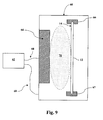
- Fig. 9 shows a general schematic as a cross-sectional view of an example DC sputtering chamber 60 for sputtering any layer in the device 10.
- a DC power source 62 is configured to control and supply DC power to the chamber 60.
- the DC power source applies a voltage to the cathode 64 to create a voltage potential between the cathode 64 and an anode formed by the chamber wall, such that the substrate is in between the cathode and anode.
- the glass substrate 12 is held between a top support 66 and a bottom support 67 via wires 68 and 69, respectively.
- the glass substrate 12 is positioned within the sputtering chamber 60 such that the sputtered layer (e.g., of the multi-layer n-type stack 16) is formed on the surface facing the cathode 64, and generally on the TCO layer 14 and RTB layer 15 (not shown) as discussed below.
- the sputtered layer e.g., of the multi-layer n-type stack 16
- a plasma field 70 is created once the sputtering atmosphere is ignited, and the plasma is sustained in response to the voltage potential between the cathode 64 and the chamber wall acting as an anode.
- the voltage potential causes the plasma ions within the plasma field 70 to accelerate toward the cathode 64, causing atoms from the cathode 64 to be ejected toward the surface on the glass substrate 12.
- the cathode 64 can be referred to as a "target" and acts as the source material for the formation of the sputtered layer on the surface of the glass substrate 12 facing the cathode 64.
- the voltage potential can be realized through the use of multiple power sources coupled together.
- the example sputtering chamber 60 is shown having a vertical orientation, although any other configuration can be utilized. After exiting the sputtering chamber 60, the substrate 12 can enter an adjacent annealing oven (not shown) to begin the annealing process.
- the glass 12 can be referred to as a "superstrate", as it is the substrate on which the subsequent layers are formed even though it faces upward to the radiation source (e.g., the sun) when the photovoltaic device 10 is in used.
- the top sheet of glass 12 can be a high-transmission glass (e.g., high transmission borosilicate glass), low-iron float glass, standard soda-lime float glass, or another highly transparent glass material.
- the glass is generally thick enough to provide support for the subsequent film layers (e.g., from about 0.5 mm to about 10 mm thick), and is substantially flat to provide a good surface for forming the subsequent film layers.
- the glass 12 can be a low iron float glass containing less than about 0.15% by weight iron (Fe), and may have a transmissiveness of about 0.9 or greater in the spectrum of interest (e.g., wavelengths from about 300 nm to about 900 nm).
- Fe iron
- the TCO layer 14 is shown on the glass 12 of the example device 10.
- the TCO layer 14 allows light to pass through with minimal absorption while also allowing electric current produced by the device 10 to travel sideways to opaque metal conductors (not shown).
- the TCO layer 14 can have a sheet resistance less than about 30 ohm per square, such as from about 4 ohm per square to about 20 ohm per square (e.g., from about 8 ohm per square to about 15 ohm per square).
- the TCO layer 14 generally includes at least one conductive oxide, such as tin oxide, zinc oxide, indium tin oxide, zinc stannate, cadmium stannate, or mixtures thereof. Additionally, the TCO layer 14 can include other conductive, transparent materials.
- the TCO layer 14 can also include dopants (e.g., fluorine, tin, etc.) and other materials, as desired.
- the TCO layer 14 can be formed by sputtering, chemical vapor deposition, spray pyrolysis, or any other suitable deposition method.
- the TCO layer 14 can be formed by sputtering (e.g., DC sputtering or RF sputtering) on the glass 12.
- a cadmium stannate layer can be formed by sputtering a hot-pressed target containing stoichiometric amounts of SnO 2 and CdO onto the glass 12 in a ratio of about 1 to about 2.
- the cadmium stannate can alternatively be prepared by using cadmium acetate and tin (II) chloride precursors by spray pyrolysis.
- the TCO layer 14 can have a thickness between about 0.1 ⁇ m and about 1 ⁇ m, for example from about 0.1 ⁇ m to about 0.5 ⁇ m, such as from about 0.25 ⁇ m to about 0.35 ⁇ m.
- a resistive transparent buffer layer 15 is shown on the TCO layer 14 on the example photovoltaic devices 10.
- the RTB layer 15 is generally more resistive than the TCO layer 14 and can help protect the device 10 from chemical interactions between the TCO layer 14 and the subsequent layers during processing of the device 10.
- the RTB layer 15 can have a sheet resistance that is greater than about 1000 ohms per square, such as from about 10 kOhms per square to about 1000 MOhms per square.
- the RTB layer 15 can also have a wide optical bandgap (e.g., greater than about 2.5 eV, such as from about 2.7 eV to about 3.5 eV).
- the presence of the RTB layer 15 between the TCO layer 14 and the multi-layer n-type stack 16 can allow for a relatively thin multi-layer n-type stack 16 to be included in the device 10 by reducing the possibility of interface defects (i.e., "pinholes" in the multi-layer n-type stack 16) creating shunts between the TCO layer 14 and the cadmium telluride layer 20.
- the RTB layer 15 allows for improved adhesion and/or interaction between the TCO layer 14 and the cadmium telluride layer 20, thereby allowing a relatively thin multi-layer n-type stack 16 to be formed thereon without significant adverse effects that would otherwise result from such a relatively thin multi-layer n-type stack 16 formed directly on the TCO layer 14.
- the RTB layer 15 can include, for instance, a combination of zinc oxide (ZnO) and tin oxide (SnO 2 ), which can be referred to as a zinc tin oxide layer ("ZTO").
- ZTO zinc tin oxide layer
- the RTB layer 15 can include more tin oxide than zinc oxide.
- the RTB layer 15 can have a composition with a stoichiometric ratio of ZnO/SnO 2 between about 0.25 and about 3, such as in about a one to two (1:2) stoichiometric ratio of tin oxide to zinc oxide.
- the RTB layer 15 can be formed by sputtering, chemical vapor deposition, spray-pyrolysis, or any other suitable deposition method.
- the RTB layer 15 can be formed by sputtering (e.g., DC sputtering or RF sputtering) on the TCO layer 14.
- the RTB layer 15 can be deposited using a DC sputtering method by applying a DC current to a metallic source material (e.g., elemental zinc, elemental tin, or a mixture thereof) and sputtering the metallic source material onto the TCO layer 14 in the presence of an oxidizing atmosphere (e.g., O 2 gas).
- O 2 gas oxygen gas
- the atmosphere can be greater than about 95% pure oxygen, such as greater than about 99%.
- the RTB layer 15 can have a thickness between about 0.075 ⁇ m and about 1 ⁇ m, for example from about 0.1 ⁇ m to about 0.5 ⁇ m. In particular embodiments, the RTB layer 15 can have a thickness between about 0.08 ⁇ m and about 0.2 ⁇ m, for example from about 0.1 ⁇ m to about 0.15 ⁇ m.
- the multi-layer n-type stack 16 can have a thickness that is less than about 0.1 ⁇ m, such as between about 10 nm and about 100 nm, such as from about 50 nm to about 80 nm, with a minimal presence of pinholes between the TCO layer 14 and the multi-layer n-type stack 16. Additionally, a multi-layer n-type stack 16 having a thickness less than about 0.1 ⁇ m reduces any absorption of radiation energy by the multi-layer n-type stack 16, effectively increasing the amount of radiation energy reaching the underlying cadmium telluride layer 20.
- a cadmium telluride layer 20 is shown on the multi-layer n-type stack 16 in the example devices 10.
- the cadmium telluride layer 20 is a p-type layer that generally includes cadmium telluride (CdTe) but may also include other materials.
- the cadmium telluride layer 20 is the photovoltaic layer that interacts with the multi-layer n-type stack 16 (i.e., the n-type layer) to produce current from the adsorption of radiation energy by absorbing the majority of the radiation energy passing into the device 10 due to its high absorption coefficient and creating electron-hole pairs.
- the cadmium telluride layer 20 can generally be formed from cadmium telluride and can have a bandgap tailored to absorb radiation energy (e.g., from about 1.4 eV to about 1.5 eV, such as about 1.45 eV) to create the maximum number of electron-hole pairs with the highest electrical potential (voltage) upon absorption of the radiation energy. Electrons may travel from the p-type side (i.e., the cadmium telluride layer 20) across the junction to the n-type side (i.e., the multi-layer n-type stack 16) and, conversely, holes may pass from the n-type side to the p-type side.
- radiation energy e.g., from about 1.4 eV to about 1.5 eV, such as about 1.45 eV
- Electrons may travel from the p-type side (i.e., the cadmium telluride layer 20) across the junction to the n-type side (i.e., the multi-
- the p-n junction formed between the multi-layer n-type stack 16 and the cadmium telluride layer 20 forms a diode in which the charge imbalance leads to the creation of an electric field spanning the p-n junction.
- Conventional current is allowed to flow in only one direction and separates the light induced electron-hole pairs.
- the cadmium telluride layer 20 can be formed by any known process, such as vapor transport deposition, chemical vapor deposition (CVD), spray pyrolysis, electrodeposition, sputtering, close-space sublimation (CSS), etc.
- the multi-layer n-type stack 16 is deposited by a sputtering and the cadmium telluride layer 20 is deposited by close-space sublimation.
- the cadmium telluride layer 20 can have a thickness between about 0.1 ⁇ m and about 10 ⁇ m, such as from about 1 ⁇ m and about 5 ⁇ m.
- the cadmium telluride layer 20 can have a thickness between about 1.5 ⁇ m and about 4 ⁇ m, such as about 2 ⁇ m to about 3 ⁇ m.
- a series of post-forming treatments can be applied to the exposed surface of the cadmium telluride layer 20. These treatments can tailor the functionality of the cadmium telluride layer 20 and prepare its surface for subsequent adhesion to the back contact layer(s) 22.
- the cadmium telluride layer 20 can be annealed at elevated temperatures (e.g., from about 350° C to about 500° C, such as from about 375° C to about 425° C) for a sufficient time (e.g., from about 1 to about 40 minutes) to create a quality p-type layer of cadmium telluride.
- annealing the cadmium telluride layer 20 decreases the deep-defect density and makes the CdTe layer more p-type. Additionally, the cadmium telluride layer 20 can recrystallize and undergo grain regrowth during annealing.
- Annealing the cadmium telluride layer 20 can be carried out in the presence of cadmium chloride in order to dope the cadmium telluride layer 20 with chloride ions.
- the cadmium telluride layer 20 can be washed with an aqueous solution containing cadmium chloride then annealed at the elevated temperature.
- the surface after annealing the cadmium telluride layer 20 in the presence of cadmium chloride, the surface can be washed to remove any cadmium oxide formed on the surface.
- This surface preparation can leave a Te-rich surface on the cadmium telluride layer 20 by removing oxides from the surface, such as CdO, CdTeO 3 , CdTe 2 O 5 , etc.
- the surface can be washed with a suitable solvent (e.g., ethylenediamine, also known as 1,2 diaminoethane or "DAE") to remove any cadmium oxide from the surface.
- a suitable solvent e.g., ethylenediamine, also known as 1,2 diaminoethane or "DAE
- copper can be added to the cadmium telluride layer 20.
- the addition of copper to the cadmium telluride layer 20 can form a surface of copper-telluride on the cadmium telluride layer 20 in order to obtain a low-resistance electrical contact between the cadmium telluride layer 20 (i.e., the p-type layer) and the back contact layer(s).
- the addition of copper can create a surface layer of cuprous telluride (Cu 2 Te) between the cadmium telluride layer 20 and the back contact layer 22 and/or can create a Cu-doped CdTe layer.
- the Te-rich surface of the cadmium telluride layer 20 can enhance the collection of current created by the device through lower resistivity between the cadmium telluride layer 20 and the back contact layer 22.
- Copper can be applied to the exposed surface of the cadmium telluride layer 20 by any process.
- copper can be sprayed or washed on the surface of the cadmium telluride layer 20 in a solution with a suitable solvent (e.g., methanol, water, or the like, or combinations thereof) followed by annealing.
- the copper may be supplied in the solution in the form of copper chloride, copper iodide, or copper acetate.
- the annealing temperature is sufficient to allow diffusion of the copper ions into the cadmium telluride layer 20, such as from about 125° C to about 300° C (e.g. from about 150° C to about 250° C) for about 5 minutes to about 30 minutes, such as from about 10 to about 25 minutes.
- a back contact layer 22 is shown on the cadmium telluride layer 20.
- the back contact layer 22 generally serves as the back electrical contact, in relation to the opposite, TCO layer 14 serving as the front electrical contact.
- the back contact layer 22 can be formed on, and in one embodiment is in direct contact with, the cadmium telluride layer 20.
- the back contact layer 22 is suitably made from one or more highly conductive materials, such as elemental nickel, chromium, copper, tin, silver, or alloys or mixtures thereof. Additionally, the back contact layer 22 can be a single layer or can be a plurality of layers.
- the back contact layer 22 can include graphite, such as a layer of carbon deposited on the p-layer followed by one or more layers of metal, such as the metals described above.
- the back contact layer 22, if made of or comprising one or more metals, is suitably applied by a technique such as sputtering or metal evaporation. If it is made from a graphite and polymer blend, or from a carbon paste, the blend or paste is applied to the semiconductor device by any suitable method for spreading the blend or paste, such as screen printing, spraying or by a "doctor" blade. After the application of the graphite blend or carbon paste, the device can be heated to convert the blend or paste into the conductive back contact layer.
- a carbon layer if used, can be from about 0.1 ⁇ m to about 10 ⁇ m in thickness, for example from about 1 ⁇ m to about 5 ⁇ m.
- a metal layer of the back contact if used for or as part of the back contact layer 22, can be from about 0.1 ⁇ m to about 1.5 ⁇ m in thickness.
- the encapsulating glass 24 is also shown in the example cadmium telluride thin film photovoltaic device 10 of Fig. 1 .
- Other components can be included in the example device 10, such as buss bars, external wiring, laser etches, etc.
- a plurality of photovoltaic cells can be connected in series in order to achieve a desired voltage, such as through an electrical wiring connection.
- Each end of the series connected cells can be attached to a suitable conductor such as a wire or bus bar, to direct the photovoltaically generated current to convenient locations for connection to a device or other system using the generated electric.
- a convenient means for achieving such series connections is to laser scribe the device to divide the device into a series of cells connected by interconnects.
- a laser can be used to scribe the deposited layers of the semiconductor device to divide the device into a plurality of series connected cells.
- Fig. 10 shows a flow diagram of an example method 30 of manufacturing a photovoltaic device according to one embodiment of the present invention.
- a TCO layer is formed on a glass superstrate at 32.
- a RTB layer is optionally formed on the TCO layer.
- a first layer of a multi-layer n-type stack is formed on the TCO layer at 36, and a second layer of a multi-layer n-type stack is formed on the TCO layer at 38.
- a third layer of a multi-layer n-type stack is formed on the TCO layer at 40.
- a cadmium telluride layer is formed on the multi-layer n-type stack at 42.
- the method 30 when including a cadmium sulfide layer and a cadmium telluride layer, the cadmium telluride layer can be annealed in the presence of cadmium chloride, washed to remove any CdO formed on the surface, and doped with copper.
- Back contact layer(s) can be applied over the cadmium telluride layer, and an encapsulating glass can be applied over the back contact layer.
- the method may also include laser scribing to form electrically isolated photovoltaic cells in the device. These electrically isolated photovoltaic cells can then be connected in series to form a photovoltaic module. Also, electrical wires can be connected to positive and negative terminals of the photovoltaic module to provide lead wires to harness electrical current produced by the photovoltaic module.
Landscapes
- Engineering & Computer Science (AREA)
- Power Engineering (AREA)
- Microelectronics & Electronic Packaging (AREA)
- Condensed Matter Physics & Semiconductors (AREA)
- Electromagnetism (AREA)
- General Physics & Mathematics (AREA)
- Computer Hardware Design (AREA)
- Physics & Mathematics (AREA)
- Chemical & Material Sciences (AREA)
- Manufacturing & Machinery (AREA)
- Crystallography & Structural Chemistry (AREA)
- Life Sciences & Earth Sciences (AREA)
- Sustainable Development (AREA)
- Sustainable Energy (AREA)
- Inorganic Chemistry (AREA)
- Photovoltaic Devices (AREA)
Applications Claiming Priority (1)
| Application Number | Priority Date | Filing Date | Title |
|---|---|---|---|
| US13/149,423 US8247686B2 (en) | 2011-05-31 | 2011-05-31 | Multi-layer N-type stack for cadmium telluride based thin film photovoltaic devices and methods of making |
Publications (2)
| Publication Number | Publication Date |
|---|---|
| EP2530726A2 true EP2530726A2 (fr) | 2012-12-05 |
| EP2530726A3 EP2530726A3 (fr) | 2014-11-19 |
Family
ID=45697796
Family Applications (1)
| Application Number | Title | Priority Date | Filing Date |
|---|---|---|---|
| EP12169573.8A Withdrawn EP2530726A3 (fr) | 2011-05-31 | 2012-05-25 | Empilement de type n multicouche pour dispositifs photovoltaïques à couche mince à base de tellurure de cadmium et procédés de fabrication |
Country Status (5)
| Country | Link |
|---|---|
| US (1) | US8247686B2 (fr) |
| EP (1) | EP2530726A3 (fr) |
| CN (1) | CN102810581B (fr) |
| AU (1) | AU2012203178A1 (fr) |
| MY (1) | MY152202A (fr) |
Families Citing this family (6)
| Publication number | Priority date | Publication date | Assignee | Title |
|---|---|---|---|---|
| US8822261B2 (en) * | 2011-09-26 | 2014-09-02 | First Solar, Inc. | Methods of making photovoltaic devices |
| ES2862900T3 (es) * | 2013-02-28 | 2021-10-08 | Ipg Photonics Corp | Acoplador de modo bajo de fibra de alta potencia |
| KR102217718B1 (ko) * | 2013-02-28 | 2021-02-19 | 아이피지 포토닉스 코포레이션 | 멀티 모드-멀티 모드 광섬유 컴바이너를 갖는 초고출력 광섬유 레이저 시스템 |
| WO2014151532A1 (fr) | 2013-03-15 | 2014-09-25 | First Solar, Inc. | Procédé de réduction de perte de couche de fenêtre de semi-conducteur durant une fabrication de dispositif photovoltaïque en couches minces, et structure de dispositif résultante |
| WO2014151594A1 (fr) | 2013-03-15 | 2014-09-25 | First Solar, Inc. | Dispositif photovoltaïque à rendement élevé utilisant du tellurure-sulfure de cadmium et procédé de fabrication |
| CN106098858A (zh) * | 2016-08-17 | 2016-11-09 | 中山瑞科新能源有限公司 | 一种碲化镉太阳能电池制备方法 |
Family Cites Families (38)
| Publication number | Priority date | Publication date | Assignee | Title |
|---|---|---|---|---|
| JPS56142684A (en) * | 1980-04-09 | 1981-11-07 | Ricoh Co Ltd | Photoelectric converter |
| JPS5745288A (en) | 1980-09-01 | 1982-03-15 | Ricoh Co Ltd | Thin film photo diode |
| US4950615A (en) | 1989-02-06 | 1990-08-21 | International Solar Electric Technology, Inc. | Method and making group IIB metal - telluride films and solar cells |
| JPH04280687A (ja) * | 1991-03-08 | 1992-10-06 | Sony Corp | p型CdSの作製方法 |
| US5261968A (en) | 1992-01-13 | 1993-11-16 | Photon Energy, Inc. | Photovoltaic cell and method |
| US5248349A (en) | 1992-05-12 | 1993-09-28 | Solar Cells, Inc. | Process for making photovoltaic devices and resultant product |
| US5474939A (en) | 1992-12-30 | 1995-12-12 | Siemens Solar Industries International | Method of making thin film heterojunction solar cell |
| US6169246B1 (en) | 1998-09-08 | 2001-01-02 | Midwest Research Institute | Photovoltaic devices comprising zinc stannate buffer layer and method for making |
| US6221495B1 (en) | 1996-11-07 | 2001-04-24 | Midwest Research Institute | Thin transparent conducting films of cadmium stannate |
| US5922142A (en) | 1996-11-07 | 1999-07-13 | Midwest Research Institute | Photovoltaic devices comprising cadmium stannate transparent conducting films and method for making |
| US6137048A (en) | 1996-11-07 | 2000-10-24 | Midwest Research Institute | Process for fabricating polycrystalline semiconductor thin-film solar cells, and cells produced thereby |
| ATE374263T1 (de) | 1999-03-29 | 2007-10-15 | Antec Solar Energy Ag | Vorrichtung und verfahren zur beschichtung von substraten durch aufdampfen mittels eines pvd- verfahrens |
| US6852614B1 (en) | 2000-03-24 | 2005-02-08 | University Of Maine | Method of manufacturing semiconductor having group II-group VI compounds doped with nitrogen |
| US6423565B1 (en) | 2000-05-30 | 2002-07-23 | Kurt L. Barth | Apparatus and processes for the massproduction of photovotaic modules |
| US6548751B2 (en) | 2000-12-12 | 2003-04-15 | Solarflex Technologies, Inc. | Thin film flexible solar cell |
| WO2002091483A2 (fr) | 2001-05-08 | 2002-11-14 | Bp Corporation North America Inc. | Dispositif photovoltaique ameliore |
| JP4621427B2 (ja) | 2001-10-05 | 2011-01-26 | ソーラー システムズ アンド エクイップメンツ エス.アール.エル. | CdTe/CdS薄膜太陽電池を大規模に生産する方法 |
| AU2002248199A1 (en) * | 2001-12-13 | 2003-06-30 | Midwest Research Institute | Semiconductor device with higher oxygen (o2) concentration within window layers and method for making |
| WO2004032189A2 (fr) | 2002-09-30 | 2004-04-15 | Miasolé | Appareil et procede de fabrication conçus pour produire a grande echelle de cellules solaires a film mince |
| US7141863B1 (en) | 2002-11-27 | 2006-11-28 | University Of Toledo | Method of making diode structures |
| US20050257824A1 (en) | 2004-05-24 | 2005-11-24 | Maltby Michael G | Photovoltaic cell including capping layer |
| US7405831B2 (en) | 2005-02-01 | 2008-07-29 | Purdue Research Foundation | Laser scanning interferometric surface metrology |
| CA2632098A1 (fr) | 2005-12-02 | 2007-06-07 | Helianthos B.V. | Pile photovoltaique |
| US7557053B2 (en) | 2006-03-13 | 2009-07-07 | Guardian Industries Corp. | Low iron high transmission float glass for solar cell applications and method of making same |
| US7601558B2 (en) | 2006-10-24 | 2009-10-13 | Applied Materials, Inc. | Transparent zinc oxide electrode having a graded oxygen content |
| US7522282B2 (en) | 2006-11-30 | 2009-04-21 | Purdue Research Foundation | Molecular interferometric imaging process and apparatus |
| US7659968B2 (en) | 2007-01-19 | 2010-02-09 | Purdue Research Foundation | System with extended range of molecular sensing through integrated multi-modal data acquisition |
| EP2034002B1 (fr) | 2007-09-04 | 2013-07-17 | Samsung Electronics Co., Ltd. | Composites d'oxyde métallique à nanocristaux et leur procédé de fabrication |
| GB0719554D0 (en) * | 2007-10-05 | 2007-11-14 | Univ Glasgow | semiconductor optoelectronic devices and methods for making semiconductor optoelectronic devices |
| US20090194165A1 (en) | 2008-01-31 | 2009-08-06 | Primestar Solar, Inc. | Ultra-high current density cadmium telluride photovoltaic modules |
| CN102037152A (zh) | 2008-03-26 | 2011-04-27 | 索莱克山特公司 | 基板太阳能电池中改进的结 |
| DE102008018928A1 (de) | 2008-04-15 | 2009-10-22 | Osram Opto Semiconductors Gmbh | Optoelektronisches Halbleiterbauelement und Verfahren zur Herstellung eines optoelektronischen Halbleiterbauelements |
| EP2452370A4 (fr) | 2009-07-10 | 2013-01-02 | First Solar Inc | Dispositifs photovoltaïques incluant du zinc |
| CN102598312B (zh) | 2009-11-05 | 2016-01-20 | 陶氏环球技术有限责任公司 | N型硫属化物组合物的制备以及它们在光伏器件中的使用 |
| US8173482B2 (en) | 2010-04-30 | 2012-05-08 | Primestar Solar, Inc. | Devices and methods of protecting a cadmium sulfide for further processing |
| US7939363B1 (en) * | 2010-10-27 | 2011-05-10 | General Electric Company | Systems and methods of intermixing cadmium sulfide layers and cadmium telluride layers for thin film photovoltaic devices |
| US20120024692A1 (en) * | 2010-10-27 | 2012-02-02 | Primestar Solar, Inc. | Mixed sputtering targets and their use in cadmium sulfide layers of cadmium telluride vased thin film photovoltaic devices |
| US7943415B1 (en) * | 2010-10-27 | 2011-05-17 | Primestar Solar Inc. | Methods of sputtering cadmium sulfide layers for use in cadmium telluride based thin film photovoltaic devices |
-
2011
- 2011-05-31 US US13/149,423 patent/US8247686B2/en active Active
-
2012
- 2012-05-11 MY MYPI2012002093 patent/MY152202A/en unknown
- 2012-05-22 AU AU2012203178A patent/AU2012203178A1/en not_active Abandoned
- 2012-05-25 EP EP12169573.8A patent/EP2530726A3/fr not_active Withdrawn
- 2012-05-30 CN CN201210172339.0A patent/CN102810581B/zh not_active Expired - Fee Related
Non-Patent Citations (1)
| Title |
|---|
| None |
Also Published As
| Publication number | Publication date |
|---|---|
| EP2530726A3 (fr) | 2014-11-19 |
| AU2012203178A1 (en) | 2012-12-20 |
| CN102810581A (zh) | 2012-12-05 |
| MY152202A (en) | 2014-08-29 |
| US20120052620A1 (en) | 2012-03-01 |
| CN102810581B (zh) | 2016-09-07 |
| US8247686B2 (en) | 2012-08-21 |
Similar Documents
| Publication | Publication Date | Title |
|---|---|---|
| US8143515B2 (en) | Cadmium telluride thin film photovoltaic devices and methods of manufacturing the same | |
| US20110139247A1 (en) | Graded alloy telluride layer in cadmium telluride thin film photovoltaic devices and methods of manufacturing the same | |
| US7943415B1 (en) | Methods of sputtering cadmium sulfide layers for use in cadmium telluride based thin film photovoltaic devices | |
| US20120061235A1 (en) | Mixed sputtering target of cadmium sulfide and cadmium telluride and methods of their use | |
| US8043955B1 (en) | Methods of forming a conductive transparent oxide film layer for use in a cadmium telluride based thin film photovoltaic device | |
| EP2448004A1 (fr) | Mélange de couches de sulfure de cadmium et couche de tellurure de cadmium pour dispositifs photovoltaïques à couche mince et leurs procédés de fabrication | |
| EP2383363B1 (fr) | Couches de sulfure de cadmium pour dispositifs photovoltaïques à couche mince en tellurure de cadmium et leur procédé de fabrication | |
| US8247683B2 (en) | Thin film interlayer in cadmium telluride thin film photovoltaic devices and methods of manufacturing the same | |
| US8247686B2 (en) | Multi-layer N-type stack for cadmium telluride based thin film photovoltaic devices and methods of making | |
| EP2371990B1 (fr) | Procédés de formation d'une couche de film d'oxyde conducteur transparent pour une utilisation dans un dispositif photovoltaïque à couche mince à base de tellurure de cadmium | |
| EP2383792A2 (fr) | Couches de sulfure de cadmium à utiliser dans les dispositifs photovoltaïques à couche mince en tellurure de cadmium et leurs procédés de fabrication | |
| US8241930B2 (en) | Methods of forming a window layer in a cadmium telluride based thin film photovoltaic device | |
| EP2402479B1 (fr) | Procédé de pulvérisation de couche mince transparente resisive pour dispositifs photovoltaïques en tellurure de cadmium | |
| US8188562B2 (en) | Multi-layer N-type stack for cadmium telluride based thin film photovoltaic devices and methods of making | |
| US20130019948A1 (en) | Stabilized back contact for photovoltaic devices and methods of their manufacture | |
| US20120024692A1 (en) | Mixed sputtering targets and their use in cadmium sulfide layers of cadmium telluride vased thin film photovoltaic devices | |
| US20130133731A1 (en) | Cadmium doped tin oxide buffer layer for thin film photovoltaic devices and their methods of manufacture | |
| US20130134037A1 (en) | Mixed targets for forming a cadmium doped tin oxide buffer layer in a thin film photovoltaic devices | |
| US20140238849A1 (en) | Methods and apparatus for controlling dopant concentration in thin films formed via sputtering deposition |
Legal Events
| Date | Code | Title | Description |
|---|---|---|---|
| PUAI | Public reference made under article 153(3) epc to a published international application that has entered the european phase |
Free format text: ORIGINAL CODE: 0009012 |
|
| AK | Designated contracting states |
Kind code of ref document: A2 Designated state(s): AL AT BE BG CH CY CZ DE DK EE ES FI FR GB GR HR HU IE IS IT LI LT LU LV MC MK MT NL NO PL PT RO RS SE SI SK SM TR |
|
| AX | Request for extension of the european patent |
Extension state: BA ME |
|
| RAP1 | Party data changed (applicant data changed or rights of an application transferred) |
Owner name: FIRST SOLAR MALAYSIA SDN.BHD |
|
| PUAL | Search report despatched |
Free format text: ORIGINAL CODE: 0009013 |
|
| AK | Designated contracting states |
Kind code of ref document: A3 Designated state(s): AL AT BE BG CH CY CZ DE DK EE ES FI FR GB GR HR HU IE IS IT LI LT LU LV MC MK MT NL NO PL PT RO RS SE SI SK SM TR |
|
| AX | Request for extension of the european patent |
Extension state: BA ME |
|
| RIC1 | Information provided on ipc code assigned before grant |
Ipc: H01L 31/18 20060101ALI20141014BHEP Ipc: H01L 31/073 20120101ALI20141014BHEP Ipc: H01L 31/0296 20060101ALI20141014BHEP Ipc: H01L 31/0392 20060101AFI20141014BHEP |
|
| 17P | Request for examination filed |
Effective date: 20150518 |
|
| RBV | Designated contracting states (corrected) |
Designated state(s): AL AT BE BG CH CY CZ DE DK EE ES FI FR GB GR HR HU IE IS IT LI LT LU LV MC MK MT NL NO PL PT RO RS SE SI SK SM TR |
|
| STAA | Information on the status of an ep patent application or granted ep patent |
Free format text: STATUS: EXAMINATION IS IN PROGRESS |
|
| 17Q | First examination report despatched |
Effective date: 20170109 |
|
| GRAP | Despatch of communication of intention to grant a patent |
Free format text: ORIGINAL CODE: EPIDOSNIGR1 |
|
| STAA | Information on the status of an ep patent application or granted ep patent |
Free format text: STATUS: GRANT OF PATENT IS INTENDED |
|
| INTG | Intention to grant announced |
Effective date: 20171010 |
|
| RIN1 | Information on inventor provided before grant (corrected) |
Inventor name: FELDMAN-PEABODY, SCOTT DANIEL Inventor name: GOSSMAN, ROBERT DWAYNE |
|
| STAA | Information on the status of an ep patent application or granted ep patent |
Free format text: STATUS: THE APPLICATION IS DEEMED TO BE WITHDRAWN |
|
| 18D | Application deemed to be withdrawn |
Effective date: 20180221 |