EP2448004A1 - Mélange de couches de sulfure de cadmium et couche de tellurure de cadmium pour dispositifs photovoltaïques à couche mince et leurs procédés de fabrication - Google Patents
Mélange de couches de sulfure de cadmium et couche de tellurure de cadmium pour dispositifs photovoltaïques à couche mince et leurs procédés de fabrication Download PDFInfo
- Publication number
- EP2448004A1 EP2448004A1 EP11185800A EP11185800A EP2448004A1 EP 2448004 A1 EP2448004 A1 EP 2448004A1 EP 11185800 A EP11185800 A EP 11185800A EP 11185800 A EP11185800 A EP 11185800A EP 2448004 A1 EP2448004 A1 EP 2448004A1
- Authority
- EP
- European Patent Office
- Prior art keywords
- layer
- cadmium
- intermixed
- cadmium telluride
- cadmium sulfide
- Prior art date
- Legal status (The legal status is an assumption and is not a legal conclusion. Google has not performed a legal analysis and makes no representation as to the accuracy of the status listed.)
- Withdrawn
Links
- MARUHZGHZWCEQU-UHFFFAOYSA-N 5-phenyl-2h-tetrazole Chemical compound C1=CC=CC=C1C1=NNN=N1 MARUHZGHZWCEQU-UHFFFAOYSA-N 0.000 title claims abstract description 200
- WUPHOULIZUERAE-UHFFFAOYSA-N 3-(oxolan-2-yl)propanoic acid Chemical compound OC(=O)CCC1CCCO1 WUPHOULIZUERAE-UHFFFAOYSA-N 0.000 title claims abstract description 147
- 229910052980 cadmium sulfide Inorganic materials 0.000 title claims abstract description 146
- 238000000034 method Methods 0.000 title claims abstract description 41
- 239000010409 thin film Substances 0.000 title claims abstract description 40
- 238000004519 manufacturing process Methods 0.000 title claims abstract description 13
- 229910052714 tellurium Inorganic materials 0.000 claims abstract description 51
- PORWMNRCUJJQNO-UHFFFAOYSA-N tellurium atom Chemical compound [Te] PORWMNRCUJJQNO-UHFFFAOYSA-N 0.000 claims abstract description 51
- NINIDFKCEFEMDL-UHFFFAOYSA-N Sulfur Chemical compound [S] NINIDFKCEFEMDL-UHFFFAOYSA-N 0.000 claims abstract description 49
- 229910052717 sulfur Inorganic materials 0.000 claims abstract description 49
- 239000011593 sulfur Substances 0.000 claims abstract description 49
- 230000003247 decreasing effect Effects 0.000 claims abstract description 27
- 238000004544 sputter deposition Methods 0.000 claims description 46
- 239000012298 atmosphere Substances 0.000 claims description 22
- 238000000137 annealing Methods 0.000 claims description 18
- 230000007423 decrease Effects 0.000 claims description 9
- 230000015572 biosynthetic process Effects 0.000 claims description 5
- CJOBVZJTOIVNNF-UHFFFAOYSA-N cadmium sulfide Chemical compound [Cd]=S CJOBVZJTOIVNNF-UHFFFAOYSA-N 0.000 claims description 5
- XSOKHXFFCGXDJZ-UHFFFAOYSA-N telluride(2-) Chemical compound [Te-2] XSOKHXFFCGXDJZ-UHFFFAOYSA-N 0.000 claims description 3
- 239000010410 layer Substances 0.000 description 468
- 239000011521 glass Substances 0.000 description 16
- 239000000463 material Substances 0.000 description 15
- 239000000758 substrate Substances 0.000 description 13
- 229910052751 metal Inorganic materials 0.000 description 11
- 239000002184 metal Substances 0.000 description 11
- 239000000203 mixture Substances 0.000 description 11
- 238000000151 deposition Methods 0.000 description 10
- 239000007789 gas Substances 0.000 description 10
- 230000005855 radiation Effects 0.000 description 10
- -1 CdS1-xTex Chemical compound 0.000 description 9
- XLOMVQKBTHCTTD-UHFFFAOYSA-N Zinc monoxide Chemical compound [Zn]=O XLOMVQKBTHCTTD-UHFFFAOYSA-N 0.000 description 9
- YKYOUMDCQGMQQO-UHFFFAOYSA-L cadmium dichloride Chemical compound Cl[Cd]Cl YKYOUMDCQGMQQO-UHFFFAOYSA-L 0.000 description 9
- RYGMFSIKBFXOCR-UHFFFAOYSA-N Copper Chemical compound [Cu] RYGMFSIKBFXOCR-UHFFFAOYSA-N 0.000 description 8
- 238000005229 chemical vapour deposition Methods 0.000 description 8
- 239000010949 copper Substances 0.000 description 8
- 229910052802 copper Inorganic materials 0.000 description 8
- 230000008569 process Effects 0.000 description 8
- XOLBLPGZBRYERU-UHFFFAOYSA-N tin dioxide Chemical compound O=[Sn]=O XOLBLPGZBRYERU-UHFFFAOYSA-N 0.000 description 8
- OKTJSMMVPCPJKN-UHFFFAOYSA-N Carbon Chemical compound [C] OKTJSMMVPCPJKN-UHFFFAOYSA-N 0.000 description 7
- 239000010408 film Substances 0.000 description 6
- 238000005546 reactive sputtering Methods 0.000 description 6
- CXKCTMHTOKXKQT-UHFFFAOYSA-N cadmium oxide Inorganic materials [Cd]=O CXKCTMHTOKXKQT-UHFFFAOYSA-N 0.000 description 5
- 230000008021 deposition Effects 0.000 description 5
- 238000010521 absorption reaction Methods 0.000 description 4
- 229910052799 carbon Inorganic materials 0.000 description 4
- XEEYBQQBJWHFJM-UHFFFAOYSA-N iron Substances [Fe] XEEYBQQBJWHFJM-UHFFFAOYSA-N 0.000 description 4
- 239000004065 semiconductor Substances 0.000 description 4
- 238000005118 spray pyrolysis Methods 0.000 description 4
- 229910001887 tin oxide Inorganic materials 0.000 description 4
- 239000011787 zinc oxide Substances 0.000 description 4
- QMMFVYPAHWMCMS-UHFFFAOYSA-N Dimethyl sulfide Chemical compound CSC QMMFVYPAHWMCMS-UHFFFAOYSA-N 0.000 description 3
- OKKJLVBELUTLKV-UHFFFAOYSA-N Methanol Chemical compound OC OKKJLVBELUTLKV-UHFFFAOYSA-N 0.000 description 3
- QVGXLLKOCUKJST-UHFFFAOYSA-N atomic oxygen Chemical compound [O] QVGXLLKOCUKJST-UHFFFAOYSA-N 0.000 description 3
- 229910052793 cadmium Inorganic materials 0.000 description 3
- 238000010549 co-Evaporation Methods 0.000 description 3
- 239000004020 conductor Substances 0.000 description 3
- 229910002804 graphite Inorganic materials 0.000 description 3
- 239000010439 graphite Substances 0.000 description 3
- 230000003993 interaction Effects 0.000 description 3
- 239000001301 oxygen Substances 0.000 description 3
- 229910052760 oxygen Inorganic materials 0.000 description 3
- 238000001552 radio frequency sputter deposition Methods 0.000 description 3
- 238000002202 sandwich sublimation Methods 0.000 description 3
- 229940071182 stannate Drugs 0.000 description 3
- 238000011282 treatment Methods 0.000 description 3
- XKRFYHLGVUSROY-UHFFFAOYSA-N Argon Chemical compound [Ar] XKRFYHLGVUSROY-UHFFFAOYSA-N 0.000 description 2
- MYMOFIZGZYHOMD-UHFFFAOYSA-N Dioxygen Chemical compound O=O MYMOFIZGZYHOMD-UHFFFAOYSA-N 0.000 description 2
- PIICEJLVQHRZGT-UHFFFAOYSA-N Ethylenediamine Chemical compound NCCN PIICEJLVQHRZGT-UHFFFAOYSA-N 0.000 description 2
- PXHVJJICTQNCMI-UHFFFAOYSA-N Nickel Chemical compound [Ni] PXHVJJICTQNCMI-UHFFFAOYSA-N 0.000 description 2
- ATJFFYVFTNAWJD-UHFFFAOYSA-N Tin Chemical compound [Sn] ATJFFYVFTNAWJD-UHFFFAOYSA-N 0.000 description 2
- CFEAAQFZALKQPA-UHFFFAOYSA-N cadmium(2+);oxygen(2-) Chemical compound [O-2].[Cd+2] CFEAAQFZALKQPA-UHFFFAOYSA-N 0.000 description 2
- 230000008859 change Effects 0.000 description 2
- 238000006243 chemical reaction Methods 0.000 description 2
- 238000010586 diagram Methods 0.000 description 2
- 239000002019 doping agent Substances 0.000 description 2
- 230000005684 electric field Effects 0.000 description 2
- 239000005329 float glass Substances 0.000 description 2
- 229910052742 iron Inorganic materials 0.000 description 2
- 150000002739 metals Chemical class 0.000 description 2
- 230000004048 modification Effects 0.000 description 2
- 238000012986 modification Methods 0.000 description 2
- 230000001590 oxidative effect Effects 0.000 description 2
- 239000000243 solution Substances 0.000 description 2
- 239000002904 solvent Substances 0.000 description 2
- 238000001228 spectrum Methods 0.000 description 2
- 239000011135 tin Substances 0.000 description 2
- 229910052718 tin Inorganic materials 0.000 description 2
- LTPQFVPQTZSJGS-UHFFFAOYSA-N 1$l^{4},3,5$l^{4},7-tetrathia-2,4,6,8-tetrazacycloocta-1,4,5,8-tetraene Chemical compound [N]1S[N]S[N]S[N]S1 LTPQFVPQTZSJGS-UHFFFAOYSA-N 0.000 description 1
- NYOZTOCADHXMEV-UHFFFAOYSA-N 2-propan-2-yltellanylpropane Chemical compound CC(C)[Te]C(C)C NYOZTOCADHXMEV-UHFFFAOYSA-N 0.000 description 1
- VEXZGXHMUGYJMC-UHFFFAOYSA-M Chloride anion Chemical compound [Cl-] VEXZGXHMUGYJMC-UHFFFAOYSA-M 0.000 description 1
- VYZAMTAEIAYCRO-UHFFFAOYSA-N Chromium Chemical compound [Cr] VYZAMTAEIAYCRO-UHFFFAOYSA-N 0.000 description 1
- JPVYNHNXODAKFH-UHFFFAOYSA-N Cu2+ Chemical compound [Cu+2] JPVYNHNXODAKFH-UHFFFAOYSA-N 0.000 description 1
- RWSOTUBLDIXVET-UHFFFAOYSA-N Dihydrogen sulfide Chemical compound S RWSOTUBLDIXVET-UHFFFAOYSA-N 0.000 description 1
- YCKRFDGAMUMZLT-UHFFFAOYSA-N Fluorine atom Chemical compound [F] YCKRFDGAMUMZLT-UHFFFAOYSA-N 0.000 description 1
- 229910018503 SF6 Inorganic materials 0.000 description 1
- BQCADISMDOOEFD-UHFFFAOYSA-N Silver Chemical compound [Ag] BQCADISMDOOEFD-UHFFFAOYSA-N 0.000 description 1
- 229910021626 Tin(II) chloride Inorganic materials 0.000 description 1
- HCHKCACWOHOZIP-UHFFFAOYSA-N Zinc Chemical compound [Zn] HCHKCACWOHOZIP-UHFFFAOYSA-N 0.000 description 1
- 239000005083 Zinc sulfide Substances 0.000 description 1
- MZEWONGNQNXVKA-UHFFFAOYSA-N [Cu].[Cu].[Te] Chemical compound [Cu].[Cu].[Te] MZEWONGNQNXVKA-UHFFFAOYSA-N 0.000 description 1
- 230000002411 adverse Effects 0.000 description 1
- 239000000956 alloy Substances 0.000 description 1
- 229910045601 alloy Inorganic materials 0.000 description 1
- 239000007864 aqueous solution Substances 0.000 description 1
- 229910052786 argon Inorganic materials 0.000 description 1
- 239000012300 argon atmosphere Substances 0.000 description 1
- 230000005540 biological transmission Effects 0.000 description 1
- 239000005388 borosilicate glass Substances 0.000 description 1
- LHQLJMJLROMYRN-UHFFFAOYSA-L cadmium acetate Chemical compound [Cd+2].CC([O-])=O.CC([O-])=O LHQLJMJLROMYRN-UHFFFAOYSA-L 0.000 description 1
- QGJOPFRUJISHPQ-NJFSPNSNSA-N carbon disulfide-14c Chemical compound S=[14C]=S QGJOPFRUJISHPQ-NJFSPNSNSA-N 0.000 description 1
- 239000000919 ceramic Substances 0.000 description 1
- 238000000224 chemical solution deposition Methods 0.000 description 1
- 239000011651 chromium Substances 0.000 description 1
- 229910052804 chromium Inorganic materials 0.000 description 1
- 229910001431 copper ion Inorganic materials 0.000 description 1
- ORTQZVOHEJQUHG-UHFFFAOYSA-L copper(II) chloride Chemical compound Cl[Cu]Cl ORTQZVOHEJQUHG-UHFFFAOYSA-L 0.000 description 1
- OPQARKPSCNTWTJ-UHFFFAOYSA-L copper(ii) acetate Chemical compound [Cu+2].CC([O-])=O.CC([O-])=O OPQARKPSCNTWTJ-UHFFFAOYSA-L 0.000 description 1
- GBRBMTNGQBKBQE-UHFFFAOYSA-L copper;diiodide Chemical compound I[Cu]I GBRBMTNGQBKBQE-UHFFFAOYSA-L 0.000 description 1
- 230000007547 defect Effects 0.000 description 1
- 230000001419 dependent effect Effects 0.000 description 1
- 238000005137 deposition process Methods 0.000 description 1
- 238000009792 diffusion process Methods 0.000 description 1
- 229910001882 dioxygen Inorganic materials 0.000 description 1
- PXJJSXABGXMUSU-UHFFFAOYSA-N disulfur dichloride Chemical compound ClSSCl PXJJSXABGXMUSU-UHFFFAOYSA-N 0.000 description 1
- 230000000694 effects Effects 0.000 description 1
- 238000009429 electrical wiring Methods 0.000 description 1
- 230000005611 electricity Effects 0.000 description 1
- 238000004070 electrodeposition Methods 0.000 description 1
- ILXWFJOFKUNZJA-UHFFFAOYSA-N ethyltellanylethane Chemical compound CC[Te]CC ILXWFJOFKUNZJA-UHFFFAOYSA-N 0.000 description 1
- 239000005357 flat glass Substances 0.000 description 1
- 239000011737 fluorine Substances 0.000 description 1
- 229910052731 fluorine Inorganic materials 0.000 description 1
- 238000010438 heat treatment Methods 0.000 description 1
- 229910000037 hydrogen sulfide Inorganic materials 0.000 description 1
- 239000012535 impurity Substances 0.000 description 1
- AMGQUBHHOARCQH-UHFFFAOYSA-N indium;oxotin Chemical compound [In].[Sn]=O AMGQUBHHOARCQH-UHFFFAOYSA-N 0.000 description 1
- 239000011261 inert gas Substances 0.000 description 1
- 238000011031 large-scale manufacturing process Methods 0.000 description 1
- 238000001755 magnetron sputter deposition Methods 0.000 description 1
- 238000001883 metal evaporation Methods 0.000 description 1
- 229910044991 metal oxide Inorganic materials 0.000 description 1
- 238000002156 mixing Methods 0.000 description 1
- 229910052759 nickel Inorganic materials 0.000 description 1
- 239000012299 nitrogen atmosphere Substances 0.000 description 1
- 230000003287 optical effect Effects 0.000 description 1
- KYKLWYKWCAYAJY-UHFFFAOYSA-N oxotin;zinc Chemical compound [Zn].[Sn]=O KYKLWYKWCAYAJY-UHFFFAOYSA-N 0.000 description 1
- 229920002959 polymer blend Polymers 0.000 description 1
- 239000002243 precursor Substances 0.000 description 1
- 238000002360 preparation method Methods 0.000 description 1
- 238000007650 screen-printing Methods 0.000 description 1
- 229910052710 silicon Inorganic materials 0.000 description 1
- 239000010703 silicon Substances 0.000 description 1
- 229910052709 silver Inorganic materials 0.000 description 1
- 239000004332 silver Substances 0.000 description 1
- 239000002356 single layer Substances 0.000 description 1
- 238000001179 sorption measurement Methods 0.000 description 1
- 238000005507 spraying Methods 0.000 description 1
- 230000007480 spreading Effects 0.000 description 1
- 238000003892 spreading Methods 0.000 description 1
- 235000011150 stannous chloride Nutrition 0.000 description 1
- 239000000126 substance Substances 0.000 description 1
- FWMUJAIKEJWSSY-UHFFFAOYSA-N sulfur dichloride Chemical compound ClSCl FWMUJAIKEJWSSY-UHFFFAOYSA-N 0.000 description 1
- SFZCNBIFKDRMGX-UHFFFAOYSA-N sulfur hexafluoride Chemical compound FS(F)(F)(F)(F)F SFZCNBIFKDRMGX-UHFFFAOYSA-N 0.000 description 1
- 229960000909 sulfur hexafluoride Drugs 0.000 description 1
- QHMQWEPBXSHHLH-UHFFFAOYSA-N sulfur tetrafluoride Chemical compound FS(F)(F)F QHMQWEPBXSHHLH-UHFFFAOYSA-N 0.000 description 1
- 239000002344 surface layer Substances 0.000 description 1
- 150000003568 thioethers Chemical class 0.000 description 1
- AXZWODMDQAVCJE-UHFFFAOYSA-L tin(II) chloride (anhydrous) Chemical compound [Cl-].[Cl-].[Sn+2] AXZWODMDQAVCJE-UHFFFAOYSA-L 0.000 description 1
- 230000007704 transition Effects 0.000 description 1
- 239000012780 transparent material Substances 0.000 description 1
- XLYOFNOQVPJJNP-UHFFFAOYSA-N water Substances O XLYOFNOQVPJJNP-UHFFFAOYSA-N 0.000 description 1
- 229910052984 zinc sulfide Inorganic materials 0.000 description 1
- UQMZPFKLYHOJDL-UHFFFAOYSA-N zinc;cadmium(2+);disulfide Chemical compound [S-2].[S-2].[Zn+2].[Cd+2] UQMZPFKLYHOJDL-UHFFFAOYSA-N 0.000 description 1
- BNEMLSQAJOPTGK-UHFFFAOYSA-N zinc;dioxido(oxo)tin Chemical compound [Zn+2].[O-][Sn]([O-])=O BNEMLSQAJOPTGK-UHFFFAOYSA-N 0.000 description 1
- DRDVZXDWVBGGMH-UHFFFAOYSA-N zinc;sulfide Chemical compound [S-2].[Zn+2] DRDVZXDWVBGGMH-UHFFFAOYSA-N 0.000 description 1
Images


Classifications
-
- C—CHEMISTRY; METALLURGY
- C23—COATING METALLIC MATERIAL; COATING MATERIAL WITH METALLIC MATERIAL; CHEMICAL SURFACE TREATMENT; DIFFUSION TREATMENT OF METALLIC MATERIAL; COATING BY VACUUM EVAPORATION, BY SPUTTERING, BY ION IMPLANTATION OR BY CHEMICAL VAPOUR DEPOSITION, IN GENERAL; INHIBITING CORROSION OF METALLIC MATERIAL OR INCRUSTATION IN GENERAL
- C23C—COATING METALLIC MATERIAL; COATING MATERIAL WITH METALLIC MATERIAL; SURFACE TREATMENT OF METALLIC MATERIAL BY DIFFUSION INTO THE SURFACE, BY CHEMICAL CONVERSION OR SUBSTITUTION; COATING BY VACUUM EVAPORATION, BY SPUTTERING, BY ION IMPLANTATION OR BY CHEMICAL VAPOUR DEPOSITION, IN GENERAL
- C23C14/00—Coating by vacuum evaporation, by sputtering or by ion implantation of the coating forming material
- C23C14/0021—Reactive sputtering or evaporation
- C23C14/0036—Reactive sputtering
- C23C14/0057—Reactive sputtering using reactive gases other than O2, H2O, N2, NH3 or CH4
-
- C—CHEMISTRY; METALLURGY
- C23—COATING METALLIC MATERIAL; COATING MATERIAL WITH METALLIC MATERIAL; CHEMICAL SURFACE TREATMENT; DIFFUSION TREATMENT OF METALLIC MATERIAL; COATING BY VACUUM EVAPORATION, BY SPUTTERING, BY ION IMPLANTATION OR BY CHEMICAL VAPOUR DEPOSITION, IN GENERAL; INHIBITING CORROSION OF METALLIC MATERIAL OR INCRUSTATION IN GENERAL
- C23C—COATING METALLIC MATERIAL; COATING MATERIAL WITH METALLIC MATERIAL; SURFACE TREATMENT OF METALLIC MATERIAL BY DIFFUSION INTO THE SURFACE, BY CHEMICAL CONVERSION OR SUBSTITUTION; COATING BY VACUUM EVAPORATION, BY SPUTTERING, BY ION IMPLANTATION OR BY CHEMICAL VAPOUR DEPOSITION, IN GENERAL
- C23C14/00—Coating by vacuum evaporation, by sputtering or by ion implantation of the coating forming material
- C23C14/0021—Reactive sputtering or evaporation
- C23C14/0036—Reactive sputtering
- C23C14/0084—Producing gradient compositions
-
- C—CHEMISTRY; METALLURGY
- C23—COATING METALLIC MATERIAL; COATING MATERIAL WITH METALLIC MATERIAL; CHEMICAL SURFACE TREATMENT; DIFFUSION TREATMENT OF METALLIC MATERIAL; COATING BY VACUUM EVAPORATION, BY SPUTTERING, BY ION IMPLANTATION OR BY CHEMICAL VAPOUR DEPOSITION, IN GENERAL; INHIBITING CORROSION OF METALLIC MATERIAL OR INCRUSTATION IN GENERAL
- C23C—COATING METALLIC MATERIAL; COATING MATERIAL WITH METALLIC MATERIAL; SURFACE TREATMENT OF METALLIC MATERIAL BY DIFFUSION INTO THE SURFACE, BY CHEMICAL CONVERSION OR SUBSTITUTION; COATING BY VACUUM EVAPORATION, BY SPUTTERING, BY ION IMPLANTATION OR BY CHEMICAL VAPOUR DEPOSITION, IN GENERAL
- C23C14/00—Coating by vacuum evaporation, by sputtering or by ion implantation of the coating forming material
- C23C14/02—Pretreatment of the material to be coated
- C23C14/024—Deposition of sublayers, e.g. to promote adhesion of the coating
-
- C—CHEMISTRY; METALLURGY
- C23—COATING METALLIC MATERIAL; COATING MATERIAL WITH METALLIC MATERIAL; CHEMICAL SURFACE TREATMENT; DIFFUSION TREATMENT OF METALLIC MATERIAL; COATING BY VACUUM EVAPORATION, BY SPUTTERING, BY ION IMPLANTATION OR BY CHEMICAL VAPOUR DEPOSITION, IN GENERAL; INHIBITING CORROSION OF METALLIC MATERIAL OR INCRUSTATION IN GENERAL
- C23C—COATING METALLIC MATERIAL; COATING MATERIAL WITH METALLIC MATERIAL; SURFACE TREATMENT OF METALLIC MATERIAL BY DIFFUSION INTO THE SURFACE, BY CHEMICAL CONVERSION OR SUBSTITUTION; COATING BY VACUUM EVAPORATION, BY SPUTTERING, BY ION IMPLANTATION OR BY CHEMICAL VAPOUR DEPOSITION, IN GENERAL
- C23C14/00—Coating by vacuum evaporation, by sputtering or by ion implantation of the coating forming material
- C23C14/06—Coating by vacuum evaporation, by sputtering or by ion implantation of the coating forming material characterised by the coating material
- C23C14/0623—Sulfides, selenides or tellurides
- C23C14/0629—Sulfides, selenides or tellurides of zinc, cadmium or mercury
-
- C—CHEMISTRY; METALLURGY
- C23—COATING METALLIC MATERIAL; COATING MATERIAL WITH METALLIC MATERIAL; CHEMICAL SURFACE TREATMENT; DIFFUSION TREATMENT OF METALLIC MATERIAL; COATING BY VACUUM EVAPORATION, BY SPUTTERING, BY ION IMPLANTATION OR BY CHEMICAL VAPOUR DEPOSITION, IN GENERAL; INHIBITING CORROSION OF METALLIC MATERIAL OR INCRUSTATION IN GENERAL
- C23C—COATING METALLIC MATERIAL; COATING MATERIAL WITH METALLIC MATERIAL; SURFACE TREATMENT OF METALLIC MATERIAL BY DIFFUSION INTO THE SURFACE, BY CHEMICAL CONVERSION OR SUBSTITUTION; COATING BY VACUUM EVAPORATION, BY SPUTTERING, BY ION IMPLANTATION OR BY CHEMICAL VAPOUR DEPOSITION, IN GENERAL
- C23C14/00—Coating by vacuum evaporation, by sputtering or by ion implantation of the coating forming material
- C23C14/22—Coating by vacuum evaporation, by sputtering or by ion implantation of the coating forming material characterised by the process of coating
- C23C14/34—Sputtering
- C23C14/3464—Sputtering using more than one target
-
- C—CHEMISTRY; METALLURGY
- C23—COATING METALLIC MATERIAL; COATING MATERIAL WITH METALLIC MATERIAL; CHEMICAL SURFACE TREATMENT; DIFFUSION TREATMENT OF METALLIC MATERIAL; COATING BY VACUUM EVAPORATION, BY SPUTTERING, BY ION IMPLANTATION OR BY CHEMICAL VAPOUR DEPOSITION, IN GENERAL; INHIBITING CORROSION OF METALLIC MATERIAL OR INCRUSTATION IN GENERAL
- C23C—COATING METALLIC MATERIAL; COATING MATERIAL WITH METALLIC MATERIAL; SURFACE TREATMENT OF METALLIC MATERIAL BY DIFFUSION INTO THE SURFACE, BY CHEMICAL CONVERSION OR SUBSTITUTION; COATING BY VACUUM EVAPORATION, BY SPUTTERING, BY ION IMPLANTATION OR BY CHEMICAL VAPOUR DEPOSITION, IN GENERAL
- C23C14/00—Coating by vacuum evaporation, by sputtering or by ion implantation of the coating forming material
- C23C14/58—After-treatment
- C23C14/5806—Thermal treatment
-
- H—ELECTRICITY
- H01—ELECTRIC ELEMENTS
- H01L—SEMICONDUCTOR DEVICES NOT COVERED BY CLASS H10
- H01L31/00—Semiconductor devices sensitive to infrared radiation, light, electromagnetic radiation of shorter wavelength or corpuscular radiation and specially adapted either for the conversion of the energy of such radiation into electrical energy or for the control of electrical energy by such radiation; Processes or apparatus specially adapted for the manufacture or treatment thereof or of parts thereof; Details thereof
- H01L31/04—Semiconductor devices sensitive to infrared radiation, light, electromagnetic radiation of shorter wavelength or corpuscular radiation and specially adapted either for the conversion of the energy of such radiation into electrical energy or for the control of electrical energy by such radiation; Processes or apparatus specially adapted for the manufacture or treatment thereof or of parts thereof; Details thereof adapted as photovoltaic [PV] conversion devices
- H01L31/06—Semiconductor devices sensitive to infrared radiation, light, electromagnetic radiation of shorter wavelength or corpuscular radiation and specially adapted either for the conversion of the energy of such radiation into electrical energy or for the control of electrical energy by such radiation; Processes or apparatus specially adapted for the manufacture or treatment thereof or of parts thereof; Details thereof adapted as photovoltaic [PV] conversion devices characterised by potential barriers
- H01L31/065—Semiconductor devices sensitive to infrared radiation, light, electromagnetic radiation of shorter wavelength or corpuscular radiation and specially adapted either for the conversion of the energy of such radiation into electrical energy or for the control of electrical energy by such radiation; Processes or apparatus specially adapted for the manufacture or treatment thereof or of parts thereof; Details thereof adapted as photovoltaic [PV] conversion devices characterised by potential barriers the potential barriers being only of the graded gap type
-
- H—ELECTRICITY
- H01—ELECTRIC ELEMENTS
- H01L—SEMICONDUCTOR DEVICES NOT COVERED BY CLASS H10
- H01L31/00—Semiconductor devices sensitive to infrared radiation, light, electromagnetic radiation of shorter wavelength or corpuscular radiation and specially adapted either for the conversion of the energy of such radiation into electrical energy or for the control of electrical energy by such radiation; Processes or apparatus specially adapted for the manufacture or treatment thereof or of parts thereof; Details thereof
- H01L31/04—Semiconductor devices sensitive to infrared radiation, light, electromagnetic radiation of shorter wavelength or corpuscular radiation and specially adapted either for the conversion of the energy of such radiation into electrical energy or for the control of electrical energy by such radiation; Processes or apparatus specially adapted for the manufacture or treatment thereof or of parts thereof; Details thereof adapted as photovoltaic [PV] conversion devices
- H01L31/06—Semiconductor devices sensitive to infrared radiation, light, electromagnetic radiation of shorter wavelength or corpuscular radiation and specially adapted either for the conversion of the energy of such radiation into electrical energy or for the control of electrical energy by such radiation; Processes or apparatus specially adapted for the manufacture or treatment thereof or of parts thereof; Details thereof adapted as photovoltaic [PV] conversion devices characterised by potential barriers
- H01L31/072—Semiconductor devices sensitive to infrared radiation, light, electromagnetic radiation of shorter wavelength or corpuscular radiation and specially adapted either for the conversion of the energy of such radiation into electrical energy or for the control of electrical energy by such radiation; Processes or apparatus specially adapted for the manufacture or treatment thereof or of parts thereof; Details thereof adapted as photovoltaic [PV] conversion devices characterised by potential barriers the potential barriers being only of the PN heterojunction type
- H01L31/073—Semiconductor devices sensitive to infrared radiation, light, electromagnetic radiation of shorter wavelength or corpuscular radiation and specially adapted either for the conversion of the energy of such radiation into electrical energy or for the control of electrical energy by such radiation; Processes or apparatus specially adapted for the manufacture or treatment thereof or of parts thereof; Details thereof adapted as photovoltaic [PV] conversion devices characterised by potential barriers the potential barriers being only of the PN heterojunction type comprising only AIIBVI compound semiconductors, e.g. CdS/CdTe solar cells
-
- H—ELECTRICITY
- H01—ELECTRIC ELEMENTS
- H01L—SEMICONDUCTOR DEVICES NOT COVERED BY CLASS H10
- H01L31/00—Semiconductor devices sensitive to infrared radiation, light, electromagnetic radiation of shorter wavelength or corpuscular radiation and specially adapted either for the conversion of the energy of such radiation into electrical energy or for the control of electrical energy by such radiation; Processes or apparatus specially adapted for the manufacture or treatment thereof or of parts thereof; Details thereof
- H01L31/18—Processes or apparatus specially adapted for the manufacture or treatment of these devices or of parts thereof
- H01L31/1828—Processes or apparatus specially adapted for the manufacture or treatment of these devices or of parts thereof the active layers comprising only AIIBVI compounds, e.g. CdS, ZnS, CdTe
-
- Y—GENERAL TAGGING OF NEW TECHNOLOGICAL DEVELOPMENTS; GENERAL TAGGING OF CROSS-SECTIONAL TECHNOLOGIES SPANNING OVER SEVERAL SECTIONS OF THE IPC; TECHNICAL SUBJECTS COVERED BY FORMER USPC CROSS-REFERENCE ART COLLECTIONS [XRACs] AND DIGESTS
- Y02—TECHNOLOGIES OR APPLICATIONS FOR MITIGATION OR ADAPTATION AGAINST CLIMATE CHANGE
- Y02E—REDUCTION OF GREENHOUSE GAS [GHG] EMISSIONS, RELATED TO ENERGY GENERATION, TRANSMISSION OR DISTRIBUTION
- Y02E10/00—Energy generation through renewable energy sources
- Y02E10/50—Photovoltaic [PV] energy
- Y02E10/543—Solar cells from Group II-VI materials
-
- Y—GENERAL TAGGING OF NEW TECHNOLOGICAL DEVELOPMENTS; GENERAL TAGGING OF CROSS-SECTIONAL TECHNOLOGIES SPANNING OVER SEVERAL SECTIONS OF THE IPC; TECHNICAL SUBJECTS COVERED BY FORMER USPC CROSS-REFERENCE ART COLLECTIONS [XRACs] AND DIGESTS
- Y02—TECHNOLOGIES OR APPLICATIONS FOR MITIGATION OR ADAPTATION AGAINST CLIMATE CHANGE
- Y02P—CLIMATE CHANGE MITIGATION TECHNOLOGIES IN THE PRODUCTION OR PROCESSING OF GOODS
- Y02P70/00—Climate change mitigation technologies in the production process for final industrial or consumer products
- Y02P70/50—Manufacturing or production processes characterised by the final manufactured product
Definitions
- the subject matter disclosed herein relates generally to intermixed thin film layers containing cadmium sulfide and cadmium telluride, along with their methods of deposition. More particularly, the subject matter disclosed herein relates to intermixed thin film layers of cadmium sulfide and cadmium telluride for use in cadmium telluride thin film photovoltaic devices and their methods of manufacture.
- V Thin film photovoltaic (PV) modules (also referred to as “solar panels") based on cadmium telluride (CdTe) paired with cadmium sulfide (CdS) as the photo-reactive components are gaining wide acceptance and interest in the industry.
- CdTe is a semiconductor material having characteristics particularly suited for conversion of solar energy to electricity.
- CdTe has an energy bandgap of about 1.45 eV, which enables it to convert more energy from the solar spectrum as compared to lower bandgap semiconductor materials historically used in solar cell applications (e.g., about 1.1 eV for silicon).
- CdTe converts radiation energy in lower or diffuse light conditions as compared to the lower bandgap materials and, thus, has a longer effective conversion time over the course of a day or in cloudy conditions as compared to other conventional materials.
- the junction of the n-type layer and the p-type layer is generally responsible for the generation of electric potential and electric current when the CdTe PV module is exposed to light energy, such as sunlight.
- the cadmium telluride (CdTe) layer and the cadmium sulfide (CdS) form a p-n heterojunction, where the CdTe layer acts as a p-type layer (i.e., a positive, electron accepting layer) and the CdS layer acts as a n-type layer (i.e., a negative, electron donating layer). Free carrier pairs are created by light energy and then separated by the p-n heterojunction to produce an electrical current.
- Intermixing at the surfaces of the cadmium sulfide and cadmium telluride layers can occur during the annealing process after deposition of the cadmium telluride layer. This intermixing can increase the minority carrier lifetime in the cadmium telluride, thereby increasing the open circuit voltage (Voc) and the fill factor, and therefore the efficiency of the device.
- intermixing caused by the annealing process is dependent upon several manufacturing variables including the annealing temperature, length of anneal, thin film and surface uniformity (especially at the p-n junction), dopant concentration(s), annealing atmosphere (e.g., humidity), etc. These manufacturing variables can create problems in forming substantially uniform PV devices during a large scale manufacturing process, resulting in varying efficiencies of the manufactured PV devices.
- Cadmium telluride thin film photovoltaic devices including an intermixed layer of cadmium sulfide and cadmium telluride between a cadmium sulfide layer and a cadmium telluride layer.
- the intermixed layer generally has an increasing tellurium concentration and decreasing sulfur concentration extending in a direction from the cadmium sulfide layer towards the cadmium telluride layer.
- Methods are also generally disclosed for manufacturing a cadmium telluride based thin film photovoltaic device having an intermixed layer of cadmium sulfide and cadmium telluride.
- the layers can either be directly contacting each other or have another layer or feature between the layers.
- these terms are simply describing the relative position of the layers to each other and do not necessarily mean “on top of” since the relative position above or below depends upon the orientation of the device to the viewer.
- the term "thin” describing any film layers of the photovoltaic device generally refers to the film layer having a thickness less than about 10 micrometers (“microns" or " ⁇ m").
- ranges and limits mentioned herein include all ranges located within the prescribed limits (i.e., subranges). For instance, a range from about 100 to about 200 also includes ranges from 110 to 150, 170 to 190, 153 to 162, and 145.3 to 149.6. Further, a limit of up to about 7 also includes a limit of up to about 5, up to 3, and up to about 4.5, as well as ranges within the limit, such as from about 1 to about 5, and from about 3.2 to about 6.5.
- cadmium telluride thin film photovoltaic devices having an intermixed layer of cadmium sulfide and cadmium telluride (CdTe/CdS), along with methods of their manufacture.
- the intermixed layer of CdTe/CdS can be positioned between a cadmium sulfide layer and the cadmium telluride layer.
- the intermixed layer can be formed during the deposition process, prior to annealing the cadmium telluride layer, to better control the stoichiometry of the junction of the cadmium sulfide layer and cadmium telluride layer. Additionally, the uniformity of the junction formed in individual devices throughout the manufacturing process can be better controlled.
- the intermixed layer of CdTe/CdS can generally have an increasing tellurium concentration and decreasing sulfur concentration extending from the cadmium sulfide layer towards the back contact layer, although several configurations can be utilized to form such an intermixed layer.
- the thickness of the intermixed layer can be configured to adjust and tailor the interaction and/or electrical field between the cadmium sulfide layer and the cadmium telluride layer.
- the intermixed layer of CdTe/CdS can have a thickness less than the thickness of the cadmium telluride layer.
- the thickness of the intermixed layer of CdTe/CdS can be between about 0.01 ⁇ m and about 1 ⁇ m, for example between about 10 nm to about 500 nm or from about 50 nm to about 250 nm.
- Fig. 1 represents an exemplary cadmium telluride thin film photovoltaic device 10 having an intermixed layer 19 of CdTe/CdS positioned between a cadmium sulfide layer 18 and a cadmium telluride layer 20.
- the intermixed layer 19 of CdTe/CdS is defined by a single thin film layer that is graded to have an increasing tellurium concentration and decreasing sulfur concentration through the thickness of the intermixed layer 19 extending from the cadmium sulfide layer 18 to the cadmium telluride layer 20.
- the intermixed layer 19 of CdTe/CdS can be represented as a CdS 1-x Te x layer, where 0 ⁇ x ⁇ 1, with increasing tellurium content (i.e., increasing the value of x) through the thickness of the intermixed layer 19 extending from the cadmium sulfide layer 18 to the cadmium telluride layer 20.
- the junction of the cadmium sulfide layer 18 and the intermixed layer 19 is primarily CdS and substantially free from tellurium (i.e., CdS 1-x Te x , where x is about 0), and the opposite surface of the intermixed layer 19, which contacts the cadmium telluride layer 20, is primarily CdTe and substantially free from sulfur (e.g., CdS 1-x Te x , where x is about 1).
- the term "substantially free” means no more than an insignificant trace amount present and encompasses completely free (e.g., 0 molar % up to 0.0001 molar %).
- the increasing tellurium concentration and decreasing sulfur concentration may be a linear change (i.e., a substantially constant rate of change) through the thickness of the graded intermixed layer 19 extending from the cadmium sulfide layer 18 to the cadmium telluride layer 20.
- the rate of increasing tellurium concentration and decreasing sulfur concentration may be varied throughout the graded intermixed layer 19.
- the rate of increasing tellurium concentration and decreasing sulfur concentration may be relatively slow (e.g., x increasing to about 0.25 or less, such as x increasing to about 0.05 to about 0.1) through the first half of the thickness, while the rate of increasing tellurium concentration and decreasing sulfur concentration may be relatively fast through the second half of the thickness.
- the rate of increasing tellurium concentration and decreasing sulfur concentration may be relatively fast (e.g., x increasing to about 0.75 or more, such as x increasing to about 0.8 to about 0.9) through the first half of the thickness, while the rate of increasing tellurium concentration and decreasing sulfur concentration may be relatively slow through the second half of the thickness.
- the intermixed layer 19 can be formed according to any process, such as co-sputtering (e.g., from a first target of cadmium sulfide and a second target of cadmium telluride), co-evaporation (e.g., from a first source of cadmium sulfide and a second source of cadmium telluride), reactive sputtering, metal-organic chemical vapor deposition (MOCVD), etc.
- co-sputtering e.g., from a first target of cadmium sulfide and a second target of cadmium telluride
- co-evaporation e.g., from a first source of cadmium sulfide and a second source of cadmium telluride
- reactive sputtering e.g., from a first source of cadmium sulfide and a second source of cadmium telluride
- MOCVD metal-organ
- reactive sputtering could be utilized to form the cadmium sulfide layer 18, then by introducing a tellurium gas source (e.g., diethyltellurium, diisopropyltelluride, or other suitable tellurium gases, or mixtures thereof) to the sputtering chamber to form an intermixed layer including tellurium into the deposited layer (e.g., in the same sputtering chamber or in a sequential sputtering chamber(s)).
- a tellurium gas source e.g., diethyltellurium, diisopropyltelluride, or other suitable tellurium gases, or mixtures thereof
- the tellurium concentration in the deposited layer can be increased by increasing the amount of tellurium in the sputtering atmosphere.
- the tellurium concentration in the sputtering atmosphere can be increased linearly, to provide for a linear increase in the tellurium concentration of the deposited intermixed layer 19 extending away from the cadmium sulfide layer 18.
- the tellurium concentration in the sputtering atmosphere can be increased to about 100% by volume, such as about 75% to about 95% by volume.
- the intermixed layer 19 can be formed by reactive sputtering a cadmium telluride target in the presence of a sulfur-containing source gas (e.g., sulfur gas, hydrogen sulfide, carbon disulfide, sulfur tetrafluoride, sulfur hexafluoride, sulfur dichloride, disulfur dichloride, dimethyl sulfide, tetrasulfur tetranitride, alkane thiols, thioethers, or other suitable sulfur-containing gases, or mixtures thereof).
- a sulfur-containing source gas e.g., sulfur gas, hydrogen sulfide, carbon disulfide, sulfur tetrafluoride, sulfur hexafluoride, sulfur dichloride, disulfur dichloride, dimethyl sulfide, tetrasulfur tetranitride, alkane thiols, thioethers, or other suitable sulfur-containing gases, or mixtures thereof).
- the sputtering atmosphere in this embodiment can have a relatively high sulfur gas concentration (e.g., about 90% to 100% by volume) upon beginning sputtering the intermixed layer that decreases during the sputtering process.
- a relatively high sulfur gas concentration e.g., about 90% to 100% by volume
- an inert gas e.g., argon
- argon can be introduced into the sputtering chamber as the sulfur-containing source gas is consumed by the reactive sputtering and/or vacuumed out of the sputtering chamber.
- Fig. 3 shows another embodiment of an intermixed layer 19 that includes a plurality of intermixed layers of increasing tellurium content (layers 1-6, respectively) formed step-wise to collectively define the intermixed layer 19.
- Each individual layer 1-6 has an increasing tellurium content and decreasing sulfur content, relative to the prior deposited layer, such that layer 2 has more tellurium content and less sulfur content than layer 1, layer 3 has more tellurium content and less sulfur content than layer 2, layer 4 has more tellurium content and less sulfur content than layer 3, layer 5 has more tellurium content and less sulfur content than layer 4, and layer 6 has more tellurium content and less sulfur content than layer 5.
- the junction of the cadmium sulfide layer 18 and the layer 1 is primarily CdS (i.e., CdS 1-x Te x , where x is 0), and the junction of the intermixed layer 19 and the cadmium telluride layer 20 is substantially free from sulfur (e.g., CdS 1-x Te x , where x is 1).
- the exemplary step-wise intermixed layer 19 shown in Fig. 3 has six layers 1-6, any number of step-wise layers can be used to form the intermixed layer 19.
- the intermixed layer can be formed, in one particular embodiment, from three intermixed layers: a first layer closest to the cadmium sulfide layer, a second layer on the first layer, and a third layer on the second layer, wherein the first layer comprises CdS 1-x Te x , where 0 ⁇ x ⁇ 0.2; the second layer comprises CdS 1-x Te x , where 0.2 ⁇ x ⁇ 0.8; and, the third layer comprises CdS 1-x Te x , where 0.8 ⁇ x ⁇ 1.
- the intermixed layer can be formed from three intermixed layers: a first layer closest to the window layer, a second layer on the first layer, and a third layer on the second layer, wherein the first layer comprises CdS 1 - x Te x , where 0 ⁇ x ⁇ , 0.1; the second layer (e.g., a transition layer) comprises CdS 1-x Te x , where 0.1 ⁇ x ⁇ 0.9; and, the third layer comprises CdS 1-x Te x , where 0.9 ⁇ x ⁇ 1.
- the intermixed layer can be defmed as a bilayer, including a first layer closest to the window layer and comprising CdS 1-x Te x , where 0 ⁇ x ⁇ 0.1; and a second layer adjacent to the cadmium telluride layer and comprising CdS 1-x Te x , where 0.9 ⁇ x ⁇ 1.
- each of the layers 1-6 can be formed of varying thickness, such as from about 1 nm to about 250 nm in thickness. In certain embodiments, the thickness of each of the layers 1-6 can be from about 10 nm to about 100 nm, for example from about 10 nm to about 50 nm. In one embodiment, each of the layers 1-6 can have substantially the same thickness.
- the step-wise plurality of layers 1-6 can generally form the intermixed layer 19 upon annealing the device 10 (e.g., post-deposition of the cadmium telluride layer 20).
- the device 10 can be annealed in the presence of cadmium chloride (CdCl 2 ), such as after deposition of the cadmium telluride layer 20.
- Annealing the device 10 can be performed by heating to an anneal temperature (e.g., about 150° C to about 600° C).
- an anneal temperature e.g., about 150° C to about 600° C.
- the cadmium telluride layer 20 and intermixed layer 19 of CdTe/CdS can be annealed less severely, such as at an anneal temperature of about 200° C to about 450° C, such as about 350° C to about 420° C, for less than about 60 minutes, such as from about 30 seconds to about 30 minutes.
- an anneal temperature of about 200° C to about 450° C, such as about 350° C to about 420° C, for less than about 60 minutes, such as from about 30 seconds to about 30 minutes.
- the less severe anneal can form the intermixed layer 19 of CdTe/CdS from the plurality of layers 1-6 without completely diffusing the cadmium telluride layer 20 into the cadmium sulfide layer 18.
- the formation of the plurality of layers 1-6 can allow for better control (e.g., stoichiometric control) of the intermixed layer 19 formed post anneal, rather than relying on the mixing of the cadmium sulfide layer 18 and the cadmium telluride layer 20 at the junction surfaces.
- the plurality of layers 1-6 can be formed according to any process, such as co-sputtering (e.g., from a first target of cadmium sulfide and a second target of cadmium telluride), co-evaporation (e.g., from a first source of cadmium sulfide and a second source of cadmium telluride), reactive sputtering, metal-organic chemical vapor deposition (MOCVD), etc, as discussed above.
- co-sputtering e.g., from a first target of cadmium sulfide and a second target of cadmium telluride
- co-evaporation e.g., from a first source of cadmium sulfide and a second source of cadmium telluride
- reactive sputtering e.g., from a first source of cadmium sulfide and a second source of cadmium telluride
- Fig. 4 shows yet another embodiment of a intermixed layer 19 formed from digital layers of alternating CdS layers 53, 55 and CdTe layers 52, 54, 56 with the CdS layers 53, 55 decreasing in thickness as the CdTe layers 52, 54, 56 increase in thickness through the thickness of the intermixed layer 19 extending from the cadmium sulfide layer 18 to the cadmium telluride layer 20.
- each of the cadmium sulfide digital layers includes CdS 1-x Te x , where 0 ⁇ x ⁇ 0.1 (e.g., substantially pure CdS), and each of the cadmium telluride digital layers includes CdS 1-x Te x , where 0.9 ⁇ x ⁇ 1 (e.g., substantially pure CdTe).
- each of the CdS layers 53, 55 are substantially free from tellurium (i.e., CdS 1-x Te x , where x is 0), and each of the CdTe layers 52, 54, 56 is substantially free from sulfur (e.g., CdS 1-x Te x , where x is 1).
- the digital layers 52-56 can intermix into the intermixed layers 19.
- the digital layers of alternating CdS layers 53, 55 and CdTe layers 52, 54, 56 with the CdS layers 53, 55 decreasing in thickness as the CdTe layers 52, 54, 56 increase in thickness through the thickness of the intermixed layer 19 form a graded structure where the tellurium concentration increases and the sulfur concentration decreases through the thickness of the intermixed layer 19 extending from the cadmium sulfide layer 18 to the cadmium telluride layer 20.
- any number of digital layers can be used to form the intermixed layer 19.
- the digital layers 52-56 can be formed according to any process, such as co-sputtering (e.g., from a first target of cadmium sulfide and a second target of cadmium telluride), co-evaporation (e.g., from a first source of cadmium sulfide and a second source of cadmium telluride), reactive sputtering, metal-organic chemical vapor deposition (MOCVD), etc, as discussed above.
- co-sputtering e.g., from a first target of cadmium sulfide and a second target of cadmium telluride
- co-evaporation e.g., from a first source of cadmium sulfide and a second source of cadmium telluride
- reactive sputtering e.g., from a first source of cadmium sulfide and a second source of cadmium telluride
- MOCVD
- the exemplary device 10 of Fig. 1 includes a top sheet of glass 12 employed as the substrate.
- the glass 12 can be referred to as a "superstrate", as it is the substrate on which the subsequent layers are formed even though it faces upward to the radiation source (e.g., the sun) when the cadmium telluride thin film photovoltaic device 10 is in used.
- the top sheet of glass 12 can be a high-transmission glass (e.g., high transmission borosilicate glass), low-iron float glass, or other highly transparent glass material.
- the glass is generally thick enough to provide support for the subsequent film layers (e.g., from about 0.5 mm to about 10 mm thick), and is substantially flat to provide a good surface for forming the subsequent film layers.
- the glass 12 can be a low iron float glass containing less than about 0.15% by weight iron (Fe), and may have a transmissiveness of about 0.9 or greater in the spectrum of interest (e.g., wavelengths from about 300 nm to about 900 nm).
- Fe iron
- a transparent conductive oxide (TCO) layer 14 is shown on the glass 12 of the exemplary device 10 of Fig. 1 .
- the TCO layer 14 allows light to pass through with minimal absorption while also allowing electric current produced by the device 10 to travel sideways to opaque metal conductors (not shown).
- the TCO layer 14 can have a sheet resistance less than about 30 ohm per square, such as from about 4 ohm per square to about 20 ohm per square (e.g., from about 8 ohm per square to about 15 ohm per square).
- the TCO layer 14 generally includes at least one conductive oxide, such as tin oxide, zinc oxide, or indium tin oxide, or mixtures thereof. Additionally, the TCO layer 14 can include other conductive, transparent materials.
- the TCO layer 14 can also include zinc stannate and/or cadmium stannate.
- the TCO layer 14 can be formed by sputtering, chemical vapor deposition, spray pyrolysis, or any other suitable deposition method.
- the TCO layer 14 can be formed by sputtering (e.g., DC sputtering or RF sputtering) on the glass 12.
- a cadmium stannate layer can be formed by sputtering a hot-pressed target containing stoichiometric amounts of Sn0 2 and CdO onto the glass 12 in a ratio of about 1 to about 2.
- the cadmium stannate can alternatively be prepared by using cadmium acetate and tin (II) chloride precursors by spray pyrolysis.
- the TCO layer 14 can have a thickness between about 0.1 ⁇ m and about 1 ⁇ m, for example from about 0.1 ⁇ m to about 0.5 ⁇ m, such as from about 0.25 ⁇ m to about 0.35 ⁇ m.
- Suitable flat glass substrates having a TCO layer 14 formed on the superstrate surface can be purchased commercially from various glass manufactures and suppliers.
- a particularly suitable glass 12 including a TCO layer 14 includes TEC 15 glass commercially available under the name TEC 15 TCO from Pilkington North America Inc. (Toledo, Ohio), which includes a TCO layer having a sheet resistance of 15 ohms per square.
- a resistive transparent buffer layer 16 (RTB layer) is shown on the TCO layer 14 on the exemplary cadmium telluride thin film photovoltaic device 10 of Fig. 1 .
- the RTB layer 16 is generally more resistive than the TCO layer 14 and can help protect the device 10 from chemical interactions between the TCO layer 14 and the subsequent layers during processing of the device 10.
- the RTB layer 16 can have a sheet resistance that is greater than about 1000 ohms per square, such as from about 10 kohms per square to about 1000 MOhms per square.
- the RTB layer 16 can also have a wide optical bandgap (e.g., greater than about 2.5 eV, such as from about 2.7 eV to about 3.5 eV).
- the presence of the RTB layer 16 between the TCO layer 14 and the cadmium sulfide layer 18 can allow for a relatively thin cadmium sulfide layer 18 to be included in the device 10 by reducing the possibility of interface defects (i.e., "pinholes" in the cadmium sulfide layer 18) creating shunts between the TCO layer 14 and the cadmium telluride layer 20.
- the RTB layer 16 allows for improved adhesion and/or interaction between the TCO layer 14 and the cadmium telluride layer 20, thereby allowing a relatively thin cadmium sulfide layer 18 to be formed thereon without significant adverse effects that would otherwise result from such a relatively thin cadmium sulfide layer 18 formed directly on the TCO layer 14.
- the RTB layer 16 can include, for instance, a combination of zinc oxide (ZnO) and tin oxide (Sn0 2 ), which can be referred to as a zinc tin oxide layer ("ZTO").
- ZTO zinc tin oxide layer
- the RTB layer 16 can include more tin oxide than zinc oxide.
- the RTB layer 16 can have a composition with a stoichiometric ratio of ZnO/SnO 2 between about 0.25 and about 3, such as in about an one to two (1:2) stoichiometric ratio of tin oxide to zinc oxide.
- the RTB layer 16 can be formed by sputtering, chemical vapor deposition, spray-pyrolysis, or any other suitable deposition method.
- the RTB layer 16 can be formed by sputtering (e.g., DC sputtering or RF sputtering) on the TCO layer 14.
- the RTB layer 16 can be deposited using a DC sputtering method by applying a DC current to a metallic source material (e.g., elemental zinc, elemental tin, or a mixture thereof) and sputtering the metallic source material onto the TCO layer 14 in the presence of an oxidizing atmosphere (e.g., O 2 gas).
- O 2 gas oxygen gas
- the atmosphere can be greater than about 95% pure oxygen, such as greater than about 99%.
- the RTB layer 16 can have a thickness between about 0.075 ⁇ m and about 1 ⁇ m, for example from about 0.1 ⁇ m to about 0.5 ⁇ m. In particular embodiments, the RTB layer 16 can have a thickness between about 0.08 ⁇ m and about 0.2 ⁇ m, for example from about 0.1 ⁇ m to about 0.15 ⁇ m.
- a cadmium sulfide layer 18 is shown on RTB layer 16 of the exemplary device 10 of Fig. 1 .
- the cadmium sulfide layer 18 is a n-type layer that generally includes cadmium sulfide (CdS) but may also include other materials, such as zinc sulfide, cadmium zinc sulfide, etc., and mixtures thereof as well as dopants and other impurities.
- the cadmium sulfide layer may include oxygen up to about 25% by atomic percentage, for example from about 5% to about 20% by atomic percentage.
- the cadmium sulfide layer 18 can have a wide band gap (e.g., from about 2.25 eV to about 2.5 eV, such as about 2.4 eV) in order to allow most radiation energy (e.g., solar radiation) to pass. As such, the cadmium sulfide layer 18 is considered a transparent layer on the device 10.
- the cadmium sulfide layer 18 can be formed by sputtering, chemical vapor deposition, chemical bath deposition, and other suitable deposition methods.
- the cadmium sulfide layer 18 can be formed by sputtering (e.g., direct current (DC) sputtering or radio frequency (RF) sputtering) on the RTB layer 16.
- Sputtering deposition generally involves ejecting material from a target, which is the material source, and depositing the ejected material onto the substrate to form the film.
- DC sputtering generally involves applying a current to a metal target (i.e., the cathode) positioned near the substrate (i.e., the anode) within a sputtering chamber to form a direct-current discharge.
- the sputtering chamber can have a reactive atmosphere (e.g., an oxygen atmosphere, nitrogen atmosphere, fluorine atmosphere) that forms a plasma field between the metal target and the substrate.
- the pressure of the reactive atmosphere can be between about 1 mTorr and about 20 mTorr for magnetron sputtering.
- the metal atoms released from the metal target can form a metallic oxide layer on the substrate.
- the current applied to the source material can vary depending on the size of the source material, size of the sputtering chamber, amount of surface area of substrate, and other variables. In some embodiments, the current applied can be from about 2 amps to about 20 amps.
- RF sputtering generally involves exciting a capacitive discharge by applying an alternating-current (AC) or radiofrequency (RF) signal between the target (e.g., a ceramic source material) and the substrate.
- the sputtering chamber can have an inert atmosphere (e.g., an argon atmosphere) having a pressure between about 1 mTorr and about 20 mTorr.
- the cadmium sulfide layer 18 can have a thickness that is less than about 0.1 ⁇ m, such as between about 10 nm and about 100 nm, such as from about 50 nm to about 80 nm, with a minimal presence of pinholes between the TCO layer 14 and the cadmium sulfide layer 18. Additionally, a cadmium sulfide layer 18 having a thickness less than about 0.1 ⁇ m reduces any absorption of radiation energy by the cadmium sulfide layer 18, effectively increasing the amount of radiation energy reaching the underlying cadmium telluride layer 20.
- the intermixed layer 19, as discussed above, is shown on the cadmium sulfide layer 18.
- a cadmium telluride layer 20 is shown on the intermixed layer 19 in the exemplary cadmium telluride thin film photovoltaic device 10 of Fig. 1 .
- the cadmium telluride layer 20 is a p-type layer that generally includes cadmium telluride (CdTe) but may also include other materials.
- the cadmium telluride layer 20 is the photovoltaic layer that interacts with the cadmium sulfide layer 18 (i.e., the n-type layer) to produce current from the adsorption of radiation energy by absorbing the majority of the radiation energy passing into the device 10 due to its high absorption coefficient and creating electron-hole pairs.
- the cadmium telluride layer 20 can generally be formed from cadmium telluride and can have a bandgap tailored to absorb radiation energy (e.g., from about 1.4 eV to about 1.5 eV, such as about 1.45 eV) to create the maximum number of electron-hole pairs with the highest electrical potential (voltage) upon absorption of the radiation energy. Electrons may travel from the p-type side (i.e., the cadmium telluride layer 20) across the junction to the n-type side (i.e., the cadmium sulfide layer 18) and, conversely, holes may pass from the n-type side to the p-type side.
- radiation energy e.g., from about 1.4 eV to about 1.5 eV, such as about 1.45 eV
- Electrons may travel from the p-type side (i.e., the cadmium telluride layer 20) across the junction to the n-type side (i.e., the
- the p-n junction formed between the cadmium sulfide layer 18 and the cadmium telluride layer 20 forms a diode in which the charge imbalance leads to the creation of an electric field spanning the p-n junction.
- Conventional current is allowed to flow in only one direction and separates the light induced electron-hole pairs.
- the cadmium telluride layer 20 can be formed by any known process, such as vapor transport deposition, chemical vapor deposition (CVD), spray pyrolysis, electrodeposition, sputtering, close-space sublimation (CSS), etc.
- the cadmium sulfide layer 18 is deposited by a sputtering and the cadmium telluride layer 20 is deposited by close-space sublimation.
- the cadmium telluride layer 20 can have a thickness between about 0.1 ⁇ m and about 10 ⁇ m, such as from about 1 ⁇ m and about 5 ⁇ m.
- the cadmium telluride layer 20 can have a thickness between about 1.5 ⁇ m and about 4 ⁇ m, such as about 2 ⁇ m to about 3 ⁇ m.
- a series of post-forming treatments can be applied to the exposed surface of the cadmium telluride layer 20. These treatments can tailor the functionality of the cadmium telluride layer 20 and prepare its surface for subsequent adhesion to the back contact layer(s) 22.
- the cadmium telluride layer 20 can be annealed at elevated temperatures (e.g., from about 350° C to about 500° C, such as from about 375° C to about 425° C) for a sufficient time (e.g., from about 1 to about 40 minutes) to create a quality p-type layer of cadmium telluride.
- annealing the cadmium telluride layer 20 decreases the deep-defect density and makes the CdTe layer more p-type. Additionally, the cadmium telluride layer 20 can recrystallize and undergo grain regrowth during annealing.
- Annealing the cadmium telluride layer 20 can be carried out in the presence of cadmium chloride in order to dope the cadmium telluride layer 20 with chloride ions.
- the cadmium telluride layer 20 can be washed with an aqueous solution containing cadmium chloride then annealed at the elevated temperature.
- the surface after annealing the cadmium telluride layer 20 in the presence of cadmium chloride, the surface can be washed to remove any cadmium oxide formed on the surface.
- This surface preparation can leave a Te-rich surface on the cadmium telluride layer 20 by removing oxides from the surface, such as CdO, CdTe0 3 , CdTe 2 0 5 , etc.
- the surface can be washed with a suitable solvent (e.g., ethylenediamine also known as 1,2 diaminoethane or "DAE") to remove any cadmium oxide from the surface.
- a suitable solvent e.g., ethylenediamine also known as 1,2 diaminoethane or "DAE
- copper can be added to the cadmium telluride layer 20.
- the addition of copper to the cadmium telluride layer 20 can form a surface of copper-telluride on the cadmium telluride layer 20 in order to obtain a low-resistance electrical contact between the cadmium telluride layer 20 (i.e., the p-type layer) and the back contact layer(s).
- the addition of copper can create a surface layer of cuprous telluride (Cu 2 Te) between the cadmium telluride layer 20 and the back contact layer 22 and/or can create a Cu-doped CdTe layer.
- the Te-rich surface of the cadmium telluride layer 20 can enhance the collection of current created by the device through lower resistivity between the cadmium telluride layer 20 and the back contact layer 22.
- Copper can be applied to the exposed surface of the cadmium telluride layer 20 by any process.
- copper can be sprayed or washed on the surface of the cadmium telluride layer 20 in a solution with a suitable solvent (e.g., methanol, water, or the like, or combinations thereof) followed by annealing.
- the copper may be supplied in the solution in the form of copper chloride, copper iodide, or copper acetate.
- the annealing temperature is sufficient to allow diffusion of the copper ions into the cadmium telluride layer 20, such as from about 125° C to about 300° C (e.g. from about 150° C to about 250° C) for about 5 minutes to about 30 minutes, such as from about 10 to about 25 minutes.
- a back contact layer 22 is shown on the cadmium telluride layer 20.
- the back contact layer 22 generally serves as the back electrical contact, in relation to the opposite, TCO layer 14 serving as the front electrical contact.
- the back contact layer 22 can be formed on, and in one embodiment is in direct contact with, the cadmium telluride layer 20.
- the back contact layer 22 is suitably made from one or more highly conductive materials, such as elemental nickel, chromium, copper, tin, silver, or alloys or mixtures thereof. Additionally, the back contact layer 22 can be a single layer or can be a plurality of layers.
- the back contact layer 22 can include graphite, such as a layer of carbon deposited on the p-layer followed by one or more layers of metal, such as the metals described above.
- the back contact layer 22, if made of or comprising one or more metals, is suitably applied by a technique such as sputtering or metal evaporation. If it is made from a graphite and polymer blend, or from a carbon paste, the blend or paste is applied to the semiconductor device by any suitable method for spreading the blend or paste, such as screen printing, spraying or by a "doctor" blade. After the application of the graphite blend or carbon paste, the device can be heated to convert the blend or paste into the conductive back contact layer.
- a carbon layer if used, can be from about 0.1 ⁇ m to about 10 ⁇ m in thickness, for example from about 1 ⁇ m to about 5 ⁇ m.
- a metal layer of the back contact if used for or as part of the back contact layer 22, can be from about 0.1 ⁇ m to about 1.5 ⁇ m in thickness.
- the encapsulating glass 24 is also shown in the exemplary cadmium telluride thin film photovoltaic device 10 of Fig. 1 .
- exemplary device 10 can include buss bars, external wiring, laser etches, etc.
- a plurality of photovoltaic cells can be connected in series in order to achieve a desired voltage, such as through an electrical wiring connection.
- Each end of the series connected cells can be attached to a suitable conductor such as a wire or bus bar, to direct the photovoltaically generated current to convenient locations for connection to a device or other system using the generated electric.
- a convenient means for achieving such series connections is to laser scribe the device to divide the device into a series of cells connected by interconnects.
- a laser can be used to scribe the deposited layers of the semiconductor device to divide the device into a plurality of series connected cells.
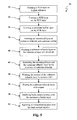
- Fig. 5 shows a flow diagram of an exemplary method 30 of manufacturing a photovoltaic device according to one embodiment of the present invention.
- a TCO layer is formed on a glass substrate at 32.
- a RTB layer is formed on the TCO layer.
- a cadmium sulfide layer is formed on the RTB layer at 36.
- An intermixed layer of cadmium telluride and cadmium sulfide can then be formed on the cadmium sulfide layer at 38.
- a cadmium telluride layer can then be formed on the intermixed layer at 40.
- the cadmium telluride layer and the intermixed layer can be annealed in the presence of cadmium chloride at 42.
- the cadmium telluride layer can then be washed at 44 to remove any CdO formed on the surface, and doped with copper at 46.
- back contact layer(s) can be applied over the cadmium telluride layer, and an encapsulating glass can be applied over the back contact layer at 50.
- the method may also include laser scribing to form electrically isolated photovoltaic cells in the device. These electrically isolated photovoltaic cells can then be connected in series to form a photovoltaic module. Also, electrical wires can be connected to positive and negative terminals of the photovoltaic module to provide lead wires to harness electrical current produced by the photovoltaic module.
Landscapes
- Chemical & Material Sciences (AREA)
- Engineering & Computer Science (AREA)
- Chemical Kinetics & Catalysis (AREA)
- Materials Engineering (AREA)
- Mechanical Engineering (AREA)
- Metallurgy (AREA)
- Organic Chemistry (AREA)
- Physics & Mathematics (AREA)
- Computer Hardware Design (AREA)
- Condensed Matter Physics & Semiconductors (AREA)
- Electromagnetism (AREA)
- General Physics & Mathematics (AREA)
- Microelectronics & Electronic Packaging (AREA)
- Power Engineering (AREA)
- Life Sciences & Earth Sciences (AREA)
- Sustainable Development (AREA)
- Sustainable Energy (AREA)
- Thermal Sciences (AREA)
- Manufacturing & Machinery (AREA)
- Photovoltaic Devices (AREA)
Applications Claiming Priority (1)
| Application Number | Priority Date | Filing Date | Title |
|---|---|---|---|
| US12/913,419 US20120024380A1 (en) | 2010-10-27 | 2010-10-27 | Intermixing of cadmium sulfide layers and cadmium telluride layers for thin film photovoltaic devices and methods of their manufacture |
Publications (1)
| Publication Number | Publication Date |
|---|---|
| EP2448004A1 true EP2448004A1 (fr) | 2012-05-02 |
Family
ID=44862598
Family Applications (1)
| Application Number | Title | Priority Date | Filing Date |
|---|---|---|---|
| EP11185800A Withdrawn EP2448004A1 (fr) | 2010-10-27 | 2011-10-19 | Mélange de couches de sulfure de cadmium et couche de tellurure de cadmium pour dispositifs photovoltaïques à couche mince et leurs procédés de fabrication |
Country Status (3)
| Country | Link |
|---|---|
| US (1) | US20120024380A1 (fr) |
| EP (1) | EP2448004A1 (fr) |
| CN (1) | CN102456754A (fr) |
Families Citing this family (9)
| Publication number | Priority date | Publication date | Assignee | Title |
|---|---|---|---|---|
| US9147793B2 (en) | 2011-06-20 | 2015-09-29 | Alliance For Sustainable Energy, Llc | CdTe devices and method of manufacturing same |
| US9397238B2 (en) * | 2011-09-19 | 2016-07-19 | First Solar, Inc. | Method of etching a semiconductor layer of a photovoltaic device |
| US9970100B2 (en) | 2012-11-16 | 2018-05-15 | The Boeing Company | Interlayer composite substrates |
| WO2014123806A2 (fr) * | 2013-02-07 | 2014-08-14 | First Solar, Inc. | Dispositif photovoltaïque à couche protectrice sur une couche de fenêtre et procédé de fabrication associé |
| WO2014151532A1 (fr) * | 2013-03-15 | 2014-09-25 | First Solar, Inc. | Procédé de réduction de perte de couche de fenêtre de semi-conducteur durant une fabrication de dispositif photovoltaïque en couches minces, et structure de dispositif résultante |
| CN104183663B (zh) * | 2013-05-21 | 2017-04-12 | 第一太阳能马来西亚有限公司 | 光伏器件及其制备方法 |
| US9139908B2 (en) | 2013-12-12 | 2015-09-22 | The Boeing Company | Gradient thin films |
| DE102014225862B4 (de) | 2014-12-15 | 2023-01-19 | China Triumph International Engineering Co., Ltd. | Verfahren zur Bildung einer Dünnschicht mit Gradient mittels Spraypyrolyse |
| CN112958150B (zh) * | 2021-03-05 | 2022-01-28 | 西南科技大学 | 乙二胺包覆硫碲化镉纳米带光催化剂的制备及放射性废水中铀的分离方法 |
Citations (3)
| Publication number | Priority date | Publication date | Assignee | Title |
|---|---|---|---|---|
| US5916375A (en) * | 1995-12-07 | 1999-06-29 | Japan Energy Corporation | Method of producing photoelectric conversion device |
| US20090242029A1 (en) * | 2008-03-26 | 2009-10-01 | Solexant Corp. | Junctions in substrate solar cells |
| US7939363B1 (en) * | 2010-10-27 | 2011-05-10 | General Electric Company | Systems and methods of intermixing cadmium sulfide layers and cadmium telluride layers for thin film photovoltaic devices |
-
2010
- 2010-10-27 US US12/913,419 patent/US20120024380A1/en not_active Abandoned
-
2011
- 2011-10-19 EP EP11185800A patent/EP2448004A1/fr not_active Withdrawn
- 2011-10-27 CN CN2011103562257A patent/CN102456754A/zh active Pending
Patent Citations (3)
| Publication number | Priority date | Publication date | Assignee | Title |
|---|---|---|---|---|
| US5916375A (en) * | 1995-12-07 | 1999-06-29 | Japan Energy Corporation | Method of producing photoelectric conversion device |
| US20090242029A1 (en) * | 2008-03-26 | 2009-10-01 | Solexant Corp. | Junctions in substrate solar cells |
| US7939363B1 (en) * | 2010-10-27 | 2011-05-10 | General Electric Company | Systems and methods of intermixing cadmium sulfide layers and cadmium telluride layers for thin film photovoltaic devices |
Non-Patent Citations (2)
| Title |
|---|
| JIAN LI ET AL: "Real time spectroscopic ellipsometry of sputtered CdTe, CdS, and CdTe1- x S x thin films for photovoltaic applications", PHYSICA STATUS SOLIDI (A), vol. 205, no. 4, 1 April 2008 (2008-04-01), pages 901 - 904, XP055015458, ISSN: 1862-6300, DOI: 10.1002/pssa.200777892 * |
| MCCANDLESS BRIAN E ET AL: "Phase behavior in the CdTe-CdS pseudobinary system", JOURNAL OF VACUUM SCIENCE AND TECHNOLOGY: PART A, AVS /AIP, MELVILLE, NY., US, vol. 20, no. 4, 1 July 2002 (2002-07-01), pages 1462 - 1467, XP012006149, ISSN: 0734-2101, DOI: 10.1116/1.1487872 * |
Also Published As
| Publication number | Publication date |
|---|---|
| US20120024380A1 (en) | 2012-02-02 |
| CN102456754A (zh) | 2012-05-16 |
Similar Documents
| Publication | Publication Date | Title |
|---|---|---|
| AU2010257207B2 (en) | Cadmium telluride thin film photovoltaic devices and methods of manufacturing the same | |
| EP2337084A2 (fr) | Couche de tellurure d'alliage gradué dans des dispositifs photovoltaïques à film mince en tellurure de cadmium et procédés de fabrication associés | |
| US20120061235A1 (en) | Mixed sputtering target of cadmium sulfide and cadmium telluride and methods of their use | |
| EP2448004A1 (fr) | Mélange de couches de sulfure de cadmium et couche de tellurure de cadmium pour dispositifs photovoltaïques à couche mince et leurs procédés de fabrication | |
| US7943415B1 (en) | Methods of sputtering cadmium sulfide layers for use in cadmium telluride based thin film photovoltaic devices | |
| US8252618B2 (en) | Methods of manufacturing cadmium telluride thin film photovoltaic devices | |
| US8043955B1 (en) | Methods of forming a conductive transparent oxide film layer for use in a cadmium telluride based thin film photovoltaic device | |
| EP2383363B1 (fr) | Couches de sulfure de cadmium pour dispositifs photovoltaïques à couche mince en tellurure de cadmium et leur procédé de fabrication | |
| US8247683B2 (en) | Thin film interlayer in cadmium telluride thin film photovoltaic devices and methods of manufacturing the same | |
| US8247686B2 (en) | Multi-layer N-type stack for cadmium telluride based thin film photovoltaic devices and methods of making | |
| EP2371990B1 (fr) | Procédés de formation d'une couche de film d'oxyde conducteur transparent pour une utilisation dans un dispositif photovoltaïque à couche mince à base de tellurure de cadmium | |
| EP2383792A2 (fr) | Couches de sulfure de cadmium à utiliser dans les dispositifs photovoltaïques à couche mince en tellurure de cadmium et leurs procédés de fabrication | |
| US8241930B2 (en) | Methods of forming a window layer in a cadmium telluride based thin film photovoltaic device | |
| EP2402479B1 (fr) | Procédé de pulvérisation de couche mince transparente resisive pour dispositifs photovoltaïques en tellurure de cadmium | |
| US20130019948A1 (en) | Stabilized back contact for photovoltaic devices and methods of their manufacture | |
| US8188562B2 (en) | Multi-layer N-type stack for cadmium telluride based thin film photovoltaic devices and methods of making | |
| US20120024692A1 (en) | Mixed sputtering targets and their use in cadmium sulfide layers of cadmium telluride vased thin film photovoltaic devices | |
| US20130133731A1 (en) | Cadmium doped tin oxide buffer layer for thin film photovoltaic devices and their methods of manufacture | |
| US20140238849A1 (en) | Methods and apparatus for controlling dopant concentration in thin films formed via sputtering deposition | |
| US20130134037A1 (en) | Mixed targets for forming a cadmium doped tin oxide buffer layer in a thin film photovoltaic devices |
Legal Events
| Date | Code | Title | Description |
|---|---|---|---|
| PUAI | Public reference made under article 153(3) epc to a published international application that has entered the european phase |
Free format text: ORIGINAL CODE: 0009012 |
|
| AK | Designated contracting states |
Kind code of ref document: A1 Designated state(s): AL AT BE BG CH CY CZ DE DK EE ES FI FR GB GR HR HU IE IS IT LI LT LU LV MC MK MT NL NO PL PT RO RS SE SI SK SM TR |
|
| AX | Request for extension of the european patent |
Extension state: BA ME |
|
| STAA | Information on the status of an ep patent application or granted ep patent |
Free format text: STATUS: THE APPLICATION IS DEEMED TO BE WITHDRAWN |
|
| 18D | Application deemed to be withdrawn |
Effective date: 20121103 |